Embed Size (px)
Citation preview

Topics will include:
Invited speakers include:
Symposium Organizers
Ilke Arslan Argonne National Laboratory, USAVeronica Augustyn North Carolina State University, USANina Balke Oak Ridge National Laboratory, USAJennifer Dionne Stanford University, USAHongyou Fan Sandia National Laboratories, USANathan Gianneschi Northwestern University, USAMartin Holt Argonne national Laboratory, USADeb Kelly The Pennsylvania State University, USAJames LeBeau Massachusetts Institute of Technology, USAAaron Lindenberg Stanford University, USAXiaoqing Pan University of California, Irvine, USA
Wenpei GaoNorth Carolina State UniversityUSATel (217) 419-9265, [email protected]
Arnaud DemortiereUniversité de Picardie Jules VerneFranceTel 03-22-82-57-94, [email protected]
Madeline Dukes
Protochips, Inc.USATel (615) 428-7971, [email protected]
Yuzi Liu
Argonne National LaboratoryUSATel (630) 252-1775, [email protected]
• New instruments for in situ imaging• Full cell design for in situ imaging of fuel cell and battery materials• Big data analysis, artificial intelligence and theoretical modeling of materials dynamics• In situ 4D STEM, ptychography and differential phase contrast imaging• Ultrafast process of materials science• Self-assembly• Ion transport• Dynamics in soft and biology materials• Phonons and vibrational properties related to bond characteristics in soft materials• Probing changes in electronic structures and magnetic states• Semiconductors and oxide devices• Materials growth aided by mechanisms revealed from in situ microscopy• Electron beam/x-ray interaction with materials
Yuki Sasaki Japan Fine Ceramics Center, JapanTao Sun University of Virginia, USAYugang Sun Temple University, USARenske van der Veen Helmholtz-Zentrum Berlin für Materialien und
Energie, GermanyMarc Willinger ETH Zürich, SwitzerlandJianbo Wu Shanghai Jiao Tong University, ChinaXianghui Xiao Brookhaven National Laboratory, USAJudith Yang University of Pittsburgh, USAXiao-Ying Yu Pacific Northwest National Laboratory, USAYimei Zhu Brookhaven National Laboratory, USA
Advancement in synchrotron X-ray techniques, microscopy and spectroscopy has extended the characterization capability to study the structure, phonon, spin, and electromagnetic field of materials with improved temporal and spatial resolution. This symposium will cover recent advances of in situ imaging techniques and highlight progress in materials design, synthesis, and engineering in catalysts and devices aided by insights gained from the state-of-the-art real-time materials characterization. This program will bring together works with an emphasis on developing and applying new methods in X-ray or electron diffraction, scanning probe microscopy, and other techniques to in situ studies of the dynamics in materials, such as the structural and chemical evolution of energy materials and catalysts, and the electronic structure of semiconductor and functional oxides. Additionally, this symposium will focus on works in designing, synthesizing new materials and optimizing materials properties by utilizing the insights on mechanisms of materials processes at different length or time scales revealed by in situ techniques. Emerging big data analysis approaches and method development presenting opportunities to aid materials design are welcomed. Discussion on experimental strategies, data analysis, and conceptual works showcasing how new in situ tools can probe exotic and critical processes in materials, such as charge and heat transfer, bonding, transport of molecule and ions, are encouraged. The symposium will identify new directions of in situ research, facilitate the application of new techniques to in situ liquid and gas phase microscopy and spectroscopy, and bridge mechanistic study with practical synthesis and engineering for materials with a broad range of applications.
Symposium CH01: Frontiers of In Situ Materials Characterization—From New Instrumentation and Method to Imaging Aided Materials Design
Joint sessions are being considered with CH03 - Advances in In Situ and Operando TEM Methods for the Study of Dynamic Processes in Materials.Also, a tutorial complementing this symposium is tentatively planned. Further information will be included in the MRS Program that will be available online in January.

Topics will include:
Invited speakers include:
Symposium Organizers
Martin Aeschlimann University of Kaiserslautern, GermanyMathew Beard National Renewable Energy Laboratory, USAEric Bittner University of Houston, USAAndrea Cavalleri Max Planck Institute for the Structure and
Dynamics of Matter, GermanyGiulio Cerullo Politecnico di milano, ItalyJenny Clark The University of Sheffield, United KingdomDavid Cooke McGill University, CanadaKeshav Dani Okinawa Institute of Science and Technology,
JapanNaomi Ginsberg University of California, Berkeley, USALibai Huang Purdue University, USAElaine Li The University of Texas at Austin, USA
Ajay Ram Srimath KandadaWake Forest UniversityUSATel (336) 758-2338, [email protected]
Margherita MaiuriPolitecnico di Milano Department of PhysicsItalyTel 39-02-2399-6249, [email protected]
Carlos Silva
Georgia Institute of Technology School of Chemistry and BiochemistryUSATel (404) 385-3410, [email protected]
Parinda Vasa
Indian Institute of Technology Bombay Department of PhysicsIndiaTel 91-22-25767556, [email protected]
• Photo-excitation dynamics in materials, probed via time-resolved spectroscopies• Structure-property relationships of ultrafast carrier dynamics via spatial probes• Multi-dimensional and other non-linear spectroscopies exploring many-body physics in materials.• Defect physics probed via ultrafast optical/opto-electronic spectroscopies• Ultrafast opto-electronic probes (Stark effects, current, interface potentials) applied to functional devices• Hybrid methods that employ optical pump and Xray/electron/THz probes.• Role of vibrations in the fate of optical excitations probed via ultrafast Raman probes• Experiments that include magnetic, electrical or pressure perturbations to the standard optical detection• Materials of interest: Energy materials such as metal halide perovskites, Excitonic materials such as 2D transition-metal dichalcogenides, quantum
materials including superconductors, quantum dots and other nanostructures, organic semiconductors.
Kalobaran Maiti Tata Institute of Fundamental Research, IndiaJennifer Oglivie University of Michigan, USATonu Pullerits Lund University, SwedenAkshay Rao University of Cambridge, United KingdomClaus Ropers University of Goettingen, GermanyD. D. Sarma Indian Institute of Science, Bangalore, IndiaJulia Stahler Humboldt-Universität zu Berlin, GermanySergei Tretiak Los Alamos National Laboratory, USACathy Wong University of Oregon, USAJoel Yuen-Zhou University of California, San Diego, USAXiaoyang Zhu Columbia University, USA
High temporal resolution and the ability to access non-linear optical responses is enabled by the use of femtosecond lasers. These have allowed spectroscopists to observe and rationalize photophysical processes in a variety of complex materials. Recent advances in laser technologies have also pushed these ultrafast probes into a wider energy range, from X-rays to THz and even ultrafast electron probes have emerged. These lead to groundbreaking and relevant discoveries in a broad variety of materials such as biological matter, energy materials and quantum materials. Keeping in mind the steady metamorphosis of these rather niche spectroscopic tools into standard material probes, this symposium takes stock of recent developments in ultrafast spectroscopic techniques in addressing contemporary issues in emerging materials. This provides an ideal platform for both ultrafast spectroscopists and material scientists to explore ways to converge established and emerging techniques for material characterization and development
Symposium CH02: Ultrafast Probes in Emerging Materials

Topics will include:
Invited speakers include:
Symposium Organizers
Trevor Almeida Commissariat à l’énergie atomique et aux énergies alternatives, France
Judy Cha Yale University, USAMiaofang Chi Oak Ridge National Laboratory, USAMichele Conroy Imperial College London, United KingdomJennifer Cookman University of Limerick, IrelandPeter Cozier Arizona State University, USAArnaud Demortiere Université de Picardie Jules Verne, FranceThierry Epicier Université de Lyon, FranceChristoph Gammer The Austrian Academy of Sciences, AustriaSang Ho Oh Sungkyunkwan University, Republic of KoreaDjamel Kaoumi North Carolina State University, USALena Kourkoutis Cornell University, USA
Leopoldo Molina-LunaDarmstadt University of TechnologyGermanyTel 0049-6151-16-20180, [email protected]
Ursel BangertUniversity of Limerick Department of PhysicsIrelandTel 00353-61-213499, [email protected]
Martial Duchamp
Nanyang Technological University School of Materials Science and Engineering (MSE)SingaporeTel 65-6316-8980, [email protected]
Andrew Minor
University of California-Berkeley & Lawrence Berkeley National Laboratory Department of Materials Science and Engineering & NCEM/MFUSATel (510) 486-2749, [email protected]
• Phase transitions and dynamic process• In situ TEM capabilities (eg. heating, cooling, ion irradiation, mechanical testing• Operando TEM capabilities (eg. biasing, magnetic fields, environments)• Advancements in in-situ holders (eg. cryogenic, vacuum transfer)• Sample preparation techniques for in situ/operando a TEM experimentations• Combination with advanced TEM techniques (phase related, spectroscopy, 4D-STEM)• Synergies with theoretical methods and data science• Computer-aided image analysis (including AI for EM) for quantitative studies• Controlled electron-beam-induced transitions
Kristian Mølhave Technical University of Denmark, DenmarkDane Morgan University of Wisconsin–Madison, USAColin Ophus Lawrence Berkeley National Laboratory, USAChristopher Regan University of California, Los Angeles, USAYukio Sato Kyushu University, JapanKiyou Shibata The University of Tokyo, JapanErdmann Spiecker Friedrich-Alexander-Universität Erlangen-
Nürnberg, GermanyMitra Taheri Johns Hopkins University, USAVasiliki Tileli École Polytechnique Fédérale de Lausanne,
SwitzerlandYang Yang The Pennsylvania State University, USAQian Yu Zhejiang University, China
There has been significant interest in the dynamic processes of smart energy materials and devices, where the properties can be controlled by an external stimulus. The possibility for example to manipulate the electronic band structure, magnetic spin and catalytic properties of such materials opens a plethora of new applications. The nature of these dynamic materials requires operando microscopy techniques to characterize their physical properties while simultaneously measuring their functional performance. Recent technological and computational advances in transmission electron microscopy are transforming what dynamic material science processes and phase changes can be explored. The focus of this symposium is on the application of in situ/operando TEM techniques that include heating, biasing, cooling, magnetic fields and mechanical testing to induce and probe phase transitions in functional materials and devices at the nanoscale that, in synergy with theoretical methods, such as first-principles calculations, phase-field, micromagnetics, finite-element based modelling and simulations, help unravel the structure and properties of materials down to the atomic scale. Furthermore, as data collection, analysis and recording of dynamic information is becoming increasingly demanding, we also welcome contributions in computer-aided image analysis and big data processing, including based on artificial intelligence algorithms, to understand the fundamental physics governing the nano- to atomic-scale phase transitions of functional materials and devices.
Symposium CH03: Advances in In Situ and Operando TEM Methods for the Study of Dynamic Processes in Materials

Topics will include:
Invited speakers include:
Symposium Organizers
Christine Aikens Kansas State University, USARaymundo Arroyave Texas A&M University, USAAlán Aspuru-Guzik University of Toronto, CanadaMuratahan Aykol Toyota Research Institute, USAAmanda Barnard The Australian National University, AustraliaPeter Battaglia DeepMind, United KingdomMiguel Bessa Delft University of Technology, NetherlandsSouvik Chakraborty Indian Institute of Technology Delhi, IndiaMaria Chan Argonne National Laboratory, USAJacqueline Cole University of Cambridge, United KingdomEkin Dogus Cubuk Google, USAPayel Das IBM T.J. Watson Research Center, USAMarjolein Dijkstra Utrecht University, NetherlandsGeorge Em Karniadakis Brown University, USAIan Foster The University of Chicago, USA
Mathieu BauchyUniversity of California, Los Angeles Civil and Environmental EngineeringUSATel (310) 825-9991, [email protected]
Mathew CherukaraArgonne National Laboratory Advanced Photon SourceUSATel (630) 252-4548, [email protected]
Grace Gu
University of California, Berkeley Mechanical EngineeringUSATel (510) 643-4996, [email protected]
Badri Narayanan
University of Louisville Mechanical EngineeringUSATel (502) 852-1469, [email protected]
• Multi-fidelity models, data-fusion, and transfer learning approaches• Machine learning to inform simulations (e.g., machine-learned interatomic forcefields)• Physics-informed machine learning and symbolic learning• "Self-driving" simulations, reinforcement learning, and robotic synthesis• Graph neural networks for materials modeling• Automatic differentiation, inverse problems, and deep generative models• Machine learning for "finding needles in haystacks" in simulation output data• Rare events sampling and automated identification of collective variables• Machine learning for structural and topology optimization• Machine-learned surrogate simulators• Natural language processing for materials modeling• Use of hardware dedicated to deep learning (e.g.,TPUs) to accelerate simulations
Rodrigo Freitas Massachusetts Institute of Technology, USARafael Gomez-Bombarelli Massachusetts Institute of Technology, USABjork Hammer Arhus University, DenmarkN M Anoop Krishnan Indian Institute of Technology Delhi, IndiaEmine Kucukbenli Harvard University, USAArtrith Nongnuch Columbia University, USARampi Ramprasad Georgia Institute of Technology, USASubramanian Sankaranarayanan
University of Illinois at Chicago, USA
Yizhou Sun University of California, Los Angeles, USARama Vasudevan Oak Ridge National Laboratory, USAWei Wang University of California, Los Angeles, USAXiaonan Wang National University of Singapore, SingaporeJie Xu Argonne National Laboratory, USALusann Yang Google, USATarek Zohdi University of California, Berkeley, USA
This symposium aims to promote an integrated vision of material design—informed by data and channeled by physics-based simulations. Although numerical simulations have revolutionized materials design, they face several challenges, including high computing cost, limited accuracy, and limited potential for inverse design. Machine learning models also suffer from some limitations, e.g., need for large, consistent, and accurate datasets, questionable extrapolations, potential violations of physics and chemistry laws, and limited interpretability. In that regard, data-driven machine learning models and knowledge-driven simulations have the potential to inform, advance, and complement each other—and to address each other’s deficiencies. This symposium builds on the idea that the lack of meaningful integration between data- and knowledge-driven modeling is a missed opportunity in materials science. This symposium will explore new modeling approaches that seamlessly combine and integrate machine learning and simulations—wherein simulation informs machine learning, machine learning advances simulations, or closed-loop integrations thereof.
Symposium DS01: Integrating Machine Learning and Simulations for Materials Modeling, Design and Manufacturing

Topics will include:
Invited speakers include:
Symposium Organizers
Radha Boya The University of Manchester, United KingdomBalamati Choudhury CSIR-National Aerospace Laboratories, IndiaJunjun Ding Alfred University, USAEdward Garboczi National Institute of Standards and Technology,
USAPhilippe H. Geubelle University of Illinois at Urbana-Champaign, USACallie Higgins National Institute of Standards and Technology, USA
Branden Kappes KMMD Consulting, USAYing Li University of Connecticut, USAWing Liu Northwestern University, USAMichael McAlpine University of Minnesota, USA
Veruska MalavéNational Institute of Standards and Technology Material Measurement Laboratory, MMLUSATel (303) 497-4598, [email protected]
Kun (Kelvin) Fu
University of DelawareUSATel (302) 831-2008, [email protected]
• Advances in additive manufacturing of multi-scale and multi-material structures and techniques (FFF, SLM, SLA, DIW, Hybrid AM).• Advances in layered/AM of polymers, metals, ceramics, biomaterials and composites.• Imaging methods for characterization of layered/AM materials (e.g., length scale modalities and computational analysis).• Virtual experimentation for layered/AM material characterization, prototypes, and cost-effective development and certification (e.g., topology
optimization, process, and testing).• Hybrid and data-driven, machine learning, and acceleration techniques to compute and optimize layered/AM material properties.• Multiscale characterization analysis for advanced layered/AM materials using physical experimental studies, atomistic- and/or continuum techniques.• Effects of complex geometries, anisotropy, heterogeneity, defects, and microstructure on layered/AM material properties: Modeling techniques.• Multiphysics computational techniques and optimization of layered/AM material properties for ultra-fast and high-resolution materials.• High-frequency asymptotic methods and electromagnetic scattering analysis of 2D metamaterial (e.g., multilayers, metasurfaces and metascreens).• Material property control and applications of novel layered/AM materials (e.g., metal-organic/hybrid, porous polymers, and functional composites).• Effects of solidification processes (time and length-scale local phenomena) and precursor properties on AM construct’s material properties.• Characterization techniques for rheology behavior affecting deposition processes of 1D, 2D, and 3D bioprinted and other soft matter constructs.• Additive manufacturing in structural (e.g., lightweight, energy-absorbing) and functional (e.g., bio-applications, energy, environment, electronics,
robotics) applications.• New materials, new techniques, curated- and comprehensive material databases, and emerging applications in additive manufacturing.
Karren More Oak Ridge National Laboratory, USA
Brian Simonds National Institute of Standards and Technology, USA
Susan Sinnott The Pennsylvania State University, USA
Hayden Taylor University of California, Berkeley, USA
Gregory Whiting University of Colorado Boulder, USA
Boris Wilthan National Institute of Standards and Technology, USA
Jinhui Yan University of Illinois at Urbana-Champaign, USA
Jing Yu Nanyang Technological University, Singapore
Xiang Zhang University of Wyoming, USA
Xuanhe Zhao Massachusetts Institute of Technology, USA
Materials layered over many length scales are ubiquitous in materials research. They can be found at the nm-scale, built up out of essentially 2D layers. They exist as polymer-matrix fiber composites, built up of 10s to 100s of many thin plies at the μm-cm scale. Additively manufactured (AM) materials fall into this class, composed of a wide spectrum of metals, ceramics, polymers, cementitious, and biological materials, which are built up layer-by-layer, from the sub-μm to m scale, to form a 3D geometry via deposition and solidification processes. All these layered materials produce new experimental and theoretical challenges as they introduce complex multiphysics that is not yet well comprehended. Hence, the development of experimental techniques and high-fidelity theoretical and computational solutions is needed to capture competing physical phenomena and scalability that lead to novel and consistent material properties. This symposium is devoted to recent advances and developments in new layered/AM materials, including design, material processing, techniques, applications, and characterization. There is a special focus on innovative constitutive and numerical paradigms for revealing the pathways towards achieving and optimizing exceptional material properties, design, and production parameters in layered/AM materials. Of high interest is the implementation of strategic physical measurements, fundamental, continuum and/or atomistic based modeling (e.g., molecular dynamics, discrete-element, finite-element, finite-volume, boundary- element, discrete element methods) of AM novel materials, quasi-2D materials, hybrids/multi-materials, and functional composites made from layered materials over any size scale. This symposium welcomes all research that motivates advances in layered/AM materials via experimentation and/or novel theoretical and computational formulations.
Symposium DS02: Advanced Manufactured Materials—Innovative Experiments, Computational Modeling and Applications
A tutorial complementing this symposium is tentatively planned. Further information will be included in the MRS Program that will be available online in January.
Vitor ColuciThe University of Campinas School of TechnologyBrazilTel (55)-(19)-21133416, [email protected]
Hui Ying Yang
Singapore University of Technology and DesignSingaporeTel (65)-6303-6663, [email protected]

Topics will include:
Invited speakers include:
Symposium Organizers
Maria Chan Argonne National Laboratory, USAStefano Curtarolo Duke University, USAPierre Darancet Argonne National Laboratory, USAGeoffroy Hautier Dartmouth College, USARun Hu Huazhong University of Science and
Technology, ChinaShenghong Ju Shanghai Jiao Tong University, ChinaTengfei Luo University of Notre Dame, USAApurva Mehta SLAC National Accelerator Laboratory, USA
Sanghamitra NeogiUniversity of Colorado Boulder Ann and H.J. Smead Aerospace Engineering SciencesUSATel (720) 517-5490, [email protected]
Ming HuUniversity of South Carolina Department of Mechanical EngineeringUSATel (803) 576-7206, [email protected]
Subramanian Sankaranarayanan
Argonne National Laboratory Theory and Modeling GroupUSATel (630) 252-4941, [email protected]
Junichiro Shiomi
The University of Tokyo Department of Mechanical EngineeringJapanTel 81-3-5841-6283-, [email protected]
• Emerging phonon dynamics in complex materials• Advances in theoretical, computational and experimental phononic property characterization techniques• Co-optimization of multiple carrier (e.g., phonon, electron) properties for thermoelectrics and other emerging technologies• Machine learning studies for prediction of thermal properties of nanostructured materials• Machine learning studies probing interaction of phonons with electrons and other quasiparticles• Data driven studies for characterization of vibrational properties of complex materials• Data mining of thermal imaging data• Phononic property data generation and sharing practices• Challenges in developing machine learning algorithms with limited training data• Novel validation approaches to test machine learning model predictions
Jesús Carrete Montaña TU Wien, AustriaKristin Persson University of California, Berkeley, USAXiulin Ruan Purdue University, USAAbhishek Singh Indian Institute of Science, Bangalore, IndiaSebastian Volz The University of Tokyo, JapanChris Wolverton Northwestern University, USAYibin Xu National Institute for Materials Science, Japan
This symposium will broadly cover current and emerging data generation techniques and data driven analysis approaches to characterize phonons, the quantized vibrations of condensed matter systems. Phonons play an increasingly important role in information-processing applications, both directly and indirectly through interactions with other quasiparticles and energy carriers. A key focus of the symposium will remain on thermal properties of materials enabling such applications. Additionally, studies exploring co-optimization of properties of multiple carriers (e.g., electron and phonon) in a variety of materials, such as thermoelectrics, wide-bandgap semiconductors, and photovoltaics, will be of particular interest. The first part of the symposium will focus on emerging theoretical and experimental techniques to calculate/measure phononic properties of complex materials. Symposium contributions should address basic science issues or highlight exploration of unusual phenomena (e.g., glass like phonon transport in crystals and/or low-symmetry materials), and address challenges in understanding the corresponding physical mechanisms. Discussion of theoretical, computational or experimental characterization techniques, challenges in data generation and applicability of emerging materials for technologies are also welcomed. The second part will focus on machine learning (ML) approaches for phononic property prediction, that are of mutual interest of the broader materials informatics communities. ML-enabled design and discovery of new materials are increasingly being facilitated by large amounts of data available through databases, however, the availability of phonon properties data is limited. Discussion of development and application of physics-based ML models that can work with sparse data and provide consistent validation approaches are particularly of interest. Contributions discussing availability of data and methods to improve data sharing practices are also of interest.
Symposium DS03: Phonon Properties of Complex Materials—Challenges in Data Generation, Data Availability and Machine Learning Approaches
A tutorial complementing this symposium is tentatively planned. Further information will be included in the MRS Program that will be available online in January.

Topics will include:
Invited speakers include:
Symposium Organizers
Alán Aspuru-Guzik University of Toronto, CanadaWilliam Chueh Stanford University, USAJacqueline Cole University of Cambridge, United KingdomAndy Cooper University of Liverpool, United KingdomAbigail Doyle Princeton University, USARafael Gomez-Bombarelli
Massachusetts Institute of Technology, USA
John Gregoire California Institute of Technology, USAJennifer Lewis Harvard University, USAElsa Olivetti Massachusetts Institute of Technology, USA
Jeffrey LopezNorthwestern University Chemical and Biological EngineeringUSATel (308) 520-3783, [email protected]
Chibueze AmanchukwuThe University of Chicago Pritzker School of Molecular EngineeringUSATel (773) 702-1892, [email protected]
Rajeev Assary
Argonne National Laboratory Materials Science DivisionUSATel (603) 252-3536, [email protected]
Tian Xie
Massachusetts Institute of Technology Computer Science and Artificial Intelligence LaboratoryUSATel (617) 909-6481, [email protected]
• Automated laboratories for energy conversion and storage materials discovery• High-throughput materials characterization• Active learning in materials discovery• High-throughput data processing• Machine learning to predict performance• Machine learning assisted molecular simulations• Natural language processing (NLP) for materials discovery• Physics-based machine learning• Visualization and interpretation of materials data• Workflows that combines experiment and simulation
Kenichi Oyaizu Waseda University, JapanKristin Persson Lawrence Berkeley National Laboratory, USACharles M. Schroeder University of Illinois at Urbana-Champaign, USATaylor Sparks University of Utah, USADee Strand Wildcat Discovery Technologies, USAZachary W. Ulissi Carnegie Mellon University, USAVenkat Viswanathan Carnegie Mellon University, USAHongliang Xin Virginia Tech, USA
This symposium will cover new advances in data-driven workflows for the development and discovery of energy conversion and storage materials. The first part of the symposium will focus on experimental work including automated and high-throughput synthesis and characterization. The second part of the symposium will focus on computational work including high-throughput computational screening and active learning workflows.
The experimentally focused portion of the symposium will highlight efforts towards data-driven discovery of materials for energy conversion and storage including photovoltaics, electrocatalysts, and electrochemical energy storage devices. To leverage computational advances and new machine learning approaches, it is vital to generate large, high-quality experimental data sets. To this end, automated and high-throughput laboratory equipment can be used to dramatically accelerate data generation in a well structured format. Symposium contributions should address the use of automated or high-throughput approaches to address basic science questions in materials for energy conversion and storage or address applications of data-driven workflows to quickly discover new materials.
The second part of this symposium will highlight computationally focused efforts towards data-driven discovery of materials for energy conversion and storage. Using data-driven approaches for materials design and discovery presents unique challenges and requires innovation in the application of existing computational tools or the development of completely new tools and workflows. Symposium contributions should address the implementation of machine learning approaches to generate or analyze computational data or address the use of high throughput workflows for energy materials screening using computational techniques such as density functional theory (DFT) calculations and molecular dynamics (MD) simulations.
Symposium DS04: Recent Advances in Data-Driven Discovery of Materials for Energy Conversion and Storage

Topics will include:
Invited speakers include:
Symposium Organizers
Andrew Blakers Australian National University, AustraliaYifeng Chen Trina Solar, USAChris Deline National Renewable Energy Laboratory, USAStefan Glunz Fraunhofer ISE, GermanyErwin Kessels Technische Universiteit Eindhoven, NetherlandsRadovan Kopecek ISC Konstanz, GermanySarah Kurtz University of California, Merced, USA
Daniel HillerTechnische Universität Dresden Institute of Semiconduc-tors and MicrosystemsGermanyTel 49-351-463-42258, [email protected]
Kaining DingForschungszentrum Jülich GmbHGermanyTel 49-2461-61-1604, [email protected]
Alison Lennon
University of New South Wales School of Photovoltaic and Renewable Energy EngineeringAustraliaTel 61-2-9385-7942, [email protected]
David Young
National Renewable Energy LaboratoryUSATel (303) 384-6621, [email protected]
• Absorber: We are interested in the development of new silicon-enabled absorbers that could offer higher absorption and/or lower Auger recombination. This also extends to alternative absorber fabrication methods such as layer separation/transfer, epitaxial wafer processes, and solid-/liquid-induced crystallization aimed at kerfless silicon or ultra-thin silicon absorbers. Research related to bulk Si defects analysis, gettering, bulk hydrogenation, and lifetime degradation / mitigation are also en
• Carrier-selective passivating contacts: We welcome contributions discussing fundamental, underlying principles of carrier-selective contacts (i.e. surface passivation, band alignment/bending, Fermi-level pinning at interfaces), innovative deposition techniques and doping methods, contact hydrogenation, new materials (including transparent electrodes and doping-free approaches) and new functionalities (temperature stability, transparency, patterned depositions).
• High efficiency device concepts: We seek contributions aimed at improved solar cell performance, including the development of novel photon management strategies (e.g. advanced surface textures, up- and down conversion), multi-junction architectures (e.g. III-V/Si or Perovskite/Si tandems), new metallization technologies (especially to passivated contacts), and back-contacted architectures.
• Module: We invite contributions dealing with module-related material aspects ranging from the interconnection and encapsulation of silicon solar cells to optical design of silicon modules (e.g. new anti-reflective coatings, albedo for bifacial modules).
• System: We also invite contributions focusing on the integration of Si modules into systems (e.g. PV-battery interface, building & vehicle integration).• Silicon and silicon-enabled photovoltaic devices, such as all-silicon tandem solar cells, X-on-silicon solar cells, new device architectures, bifacial cells,
silicon nanowires/nanocrystals solar cells, and thin-film silicon solar cells. Absorber, doping, contact, passivation, transparent conductor, and metallization materials for silicon (or tandem) photovoltaic devices.
• Silicon film materials such as amorphous silicon, nanocrystalline silicon, silicon carbides and oxides, epitaxial silicon and epitaxial layers on silicon, silicon-germanium, barium-disilicide, silicon clathrates and silicon-(carbon-)tin alloys. Methods of making and/or doping silicon including (PE)CVD, kerfless wafering, laser- and metal-induced crystallization, and implantation.
• Characterization and modeling of the structural, mechanical, electrical, and optical properties of silicon-related materials and devices. Material focused techno-economic and life-cycle analysis of emerging concepts as well as recycling aspects of PV materials.
Agata Lachowicz Swiss Center for Electronics and Microtechnology, Switzerland
John Murphy University of Warwick, United KingdomBonna Newman Netherlands Organisation for Applied Scientific
Research, NetherlandsUwe Rau Forschungszentrum Jülich GmbH, GermanyCassidy Sainsbury Sinton Instruments, USAAdele Tamboli National Renewable Energy Laboratory, USALoic Tous imec, Belgium
Silicon continues to dominate the photovoltaic market with increasing efficiencies and lower costs combined with excellent reliability. Further advancement of silicon photovoltaics will be driven by the ability to develop concepts at the cell, module and system level that further increase yield, reduce cost and extend reliability. To maintain this trend, sustained material research in key and emerging areas along the value chain is vital, including: (i) new silicon-enabled absorbers as well as the understanding and mitigation of bulk absorber material defects; (ii) carrier-selective, passivating contact layers and stacks for high voltage devices; (iii) high efficiency device concepts including, but not limited to, photon management, multi-junction solar cells and new metallization schemes; and (iv) silicon PV module and system related material research.This symposium is focused on these themes, and especially welcomes scientific and technological contributions aimed at (a) increasing the conversion efficiency and lowering the costs, (b) involving cross-cutting developments from other technologies, (c) addressing material requirements for PV system integration, and (d) modeling and characterization aligned with the aforementioned topics.
Symposium EN01: Silicon for Photovoltaics

Topics will include:
Invited speakers include:
Symposium Organizers
Rebecca Anthony Michigan State University, USAHarry Atwater California Institute of Technology, USANed Ekins-Daukes University of New South Wales, AustraliaAnna Fontcuberta i Morral
École Polytechnique Fédérale de Lausanne, Switzerland
Sophia Haussener École Polytechnique Fédérale de Lausanne, Switzerland
Hannah Joyce Cambridge University, United KingdomRehan Kapadia University of Southern California, USAMinjoo Lawrence Lee University of Illinois at Urbana-Champaign, USAMarina Leite University of California, Davis, USA
Vijay ParameshwaranU.S. Army Research LaboratoryUSATel (301) 394-0927, [email protected]
Esther Alarcon-LladoAMOLFNetherlandsTel 31-20-7547320, [email protected]
Todd Deutsch
National Renewable Energy LaboratoryUSATel (303) 275-3727, [email protected]
Shu Hu
Yale UniversityUSATel (203) 432-4764, [email protected]
• Molecular beam epitaxy (MBE) and metalorganic chemical vapor deposition (MOCVD) of III-V semiconductors for energy conversion• Alternative crystal growth methods, such as electrochemical crystal growth, colloidal nanocrystal synthesis, liquid phase epitaxy, halide chemical vapor
deposition, and vapor-liquid-solid (VLS) nanowire growth• Characterization methods in determining structure and properties, including in-situ methods• Modeling methods, including molecular dynamics (MD) for crystal growth and device/band engineering modeling for junctions• III-V semiconductors in photovoltaics; with variants for thermophotovoltaics and betavoltaics• Interface engineering of III-V materials with electrocatalysts and electrolytes for solar-to-fuels technologies• Modeling and experiments of coupling III-V semiconductors to non-conventional primary power sources (e.g. IR radiation and beta particle emitters)• Integration with non-conventional/non-epitaxial substrates in device implementation• Processing technologies around III-V crystals for energy applications integration• Systems-level coupling to energy storage systems• Technoeconomic analysis of using III-V materials for energy conversion (resource cost, efficiency and other metrics), synthesis and manufacturing
methods to reduce cost• Investigations of micro/nanoscale morphologies on performance• Earth-abundant alternatives to III-V semiconductors
Stephen Maldonado University of Michigan–Ann Arbor, USAZetian Mi University of Michigan–Ann Arbor, USASudha Mokkapati Monash University, AustraliaAaron Ptak National Renewable Energy Laboratory, USAMichael Spencer Morgan State University, USAMyles Steiner National Renewable Energy Laboratory, USAMahendra Sunkara University of Louisville, USAKimberly Dick Thelander Lund University, SwedenXiaowang Zhou Sandia National Laboratories, USA
III-V semiconductors (with cation as Al/Ga/In, and anion as N/P/As/Sb) while traditionally explored for electronic and photonic devices, have not seen much development for energy conversion technologies apart from multijunction photovoltaic stacks. Due to their superior light absorption, charge transfer, bandgap energy tunability, epitaxial crystal relationships, and single crystal nanoscale growth properties, this materials system offers promise within integration in a variety of energy conversion technologies. This includes photovoltaics, solar-to-fuels systems, thermophotovoltaics, and betavoltaics. Therefore, an emerging nexus of materials growth, device development, and systems engineering around III-V semiconductors for these energy conversion applications has the potential to shape these technologies in the present and future, and form a research core of utilizing these materials in novel ways to support development for a variety of energy conversion systems. This symposium will bring together researchers in III-V materials growth, materials characterization, device design, systems applications, and broader overviews in renewable energy and resource utilization with these materials.
Symposium EN02: III-V Semiconductors for Energy Conversion Technologies

Topics will include:
Invited speakers include:
Symposium Organizers
Shiyou Chen Fudan University, ChinaNicolas Gaillard University of Hawai‘I, USAJohn Gregoire California Institute of Technology, USAMaarja Grossberg Tallinn University of Technology, EstoniaXiaojing Hao University of New South Wales, AustraliaSophia Haussener École Polytechnique Fédérale de Lausanne,
SwitzerlandRobert Hoye Imperial College London, United KingdomPaul Maggard North Carolina State University, USAJon Major University of Liverpool, United KingdomRoland Marschall University of Bayreuth, USAHiroaki Misawa Hokkaido University, Japan
Sage BauersNational Renewable Energy LaboratoryUSATel (530) 575-6395, [email protected]
Kazuhiko MaedaTokyo Institute of TechnologyJapanTel 03-5734-2239, [email protected]
Jeff Neaton
Lawrence Berkeley National LaboratoryUSATel (510) 486-4527, [email protected]
Lydia Wong
Nanyang Technological UniversitySingaporeTel (65)-6513-8292, [email protected]
• Materials chemistry & physics, interface science, photoelectrochemistry• Theory, computation, synthesis, characterization, modelling, and device integration• Photon, electron, and chemical processes in PEC materials and cells• Absorber materials, photocatalysts, contact layers, transparent conductors• Aqueous stability, grain boundariess, defects & dopants, surface passivation• Data-driven, high-throughput computational and experimental methods
David Mitzi Duke University, USAFrank Osterloh University of California, Davis, USAAnnabella Selloni Princeton University, USAByungha Shin Korea Advanced Institute of Science and
Technology, Republic of KoreaIssei Suzuki Tohoku University, JapanAdele Tamboli National Renewable Energy Laboratory, USAJiang Tang Huazhong University of Science and
Technology, ChinaRoel van de Krol Helmholtz-Zentrum Berlin für Materialien und
Energie, GermanyJulia Wiktor Chalmers University of Technology, SwedenRong Xu Nanyang Technological University, Singapore
This symposium is jointly organized by MRS and MRS-Singapore (MRSS). Photovoltaic (PV) and photoelectrochemical (PEC) solar cells are energy technologies that convert sunlight into electricity or fuels. The main component common to both PV and PEC technologies is the semiconductor absorber material, where the sunlight is absorbed and photoactivated charge carriers are transported. Established absorber technologies have matured to the point where PV is now cost competitive against all other energy sources for electricity production, but work remains to achieve even higher efficiencies and lower costs. On the other hand, the technology of generating fuels from photocatalytic processes is far less mature than energy generated by PV, due to stringent selection criteria for suitable photoelectrodes. In addition to solar spectrum-matched band gaps and favorable charge transport required for PV technologies, PEC absorbers must also have band edges that can drive chemistry with photogenerated carriers, sufficient stability to survive in aqueous environments, and catalytic selectivity toward the desired reaction. Thus, additional research and development of emerging inorganic semiconductor absorber materials is needed to diversify the portfolio of existing PV—and especially PEC—solar cell technologies.
This symposium will cover all aspects of emerging inorganic photoabsorber materials, with particular emphasis on materials for photovoltaic and photoelectrochemical solar cells. A wide range of emerging materials will be discussed including SnS, ZnTe, Cu2O, Sb2Se3, Bi2S3, MoSe2, ZnSnN2, FeWO4, CuBi2O4, CuSbS2, BiVO4, AgBiS2, CsPbCl3, Cu2ZnSnS4, Cu2BaSnS4, as well as other novel oxides, chalcogenides, nitrides, and phosphides. Contributions on emerging contacts, buffers, transparent conductors, and other supporting materials for semiconductors such as, Si, CdTe, CIGS, and III-V PV absorbers are of interest, but not these well-established absorbers themselves. This year, we will also consider contributions focusing on emerging photocatalysts, absorber/catalyst interactions, catalyst surface decoration, PEC cell designs, device encapsulants, and other materials supporting photocatalytic processes, in addition to the photoelectrochemical cell absorbers. Contributions on emerging materials for other optoelectronic energy conversion technologies, such as solid-state lighting and photodetectors are also welcome.
Symposium EN03: Emerging Inorganic Semiconductors for Solar Energy and Fuels
A tutorial complementing this symposium is tentatively planned. Further information will be included in the MRS Program that will be available online in January.

Topics will include:
Invited speakers include:
Symposium Organizers
Natalie Banerji University of Bern, SwitzerlandMelanie Bertrand Armor, FranceJean Luc Bredas The University of Arizona, USADong Hoon Choi Korea University, Republic of KoreaXugang Guo Southern University of Science and Technology,
ChinaBumjoon Kim Korea Advanced Institute of Science and
Technology, Republic of KoreaMario Leclerc Université Laval, CanadaKwanghee Lee Gwangju Institute of Science and Technology,
Republic of KoreaPooi See Lee Nanyang Technological University, Singapore
Han Young WooKorea UniversityRepublic of KoreaTel 82-10-7343-0960, [email protected]
Derya BaranKing Abdullah University of Science and TechnologySaudi ArabiaTel 966-(0)12-808-7238, [email protected]
Jung-Yong Lee
Korea Advanced Institute of Science and TechnologyRepublic of KoreaTel 82-10-9341-1834, [email protected]
Gregory C. Welch
University of CalgaryCanadaTel 403-210-7603, [email protected]
• Synthesis of new organic (and polymeric) photovoltaic materials• Device fabrication and photovoltaic characteristics• Fundamentals for charge generation, transport, recombination and extraction• Photovoltaic applications for flexible, stretchable and wearable devices• Mechanical properties and device stability• Film morphology control and characterization• Device dynamics by transient absorption and time-resolved spectroscopy• Theoretical modeling and calculation of photovoltaic materials and characteristics
Dongling Ma Institut National de la Recherche Scientifique, Canada
Thuc-Quyen Nguyen University of California, Santa Barbara, USABrendan O`Connor North Carolina State University, USAJean-Rémi Pouliot Brilliant Matters, CanadaErin Ratcliff University of Arizona, USASafa Shoaee University of Potsdam, GermanyKeisuke Tajima RIKEN, JapanWei You University of North Carolina at Chapel Hill, USAYingping Zou Central South University, China
Next-generation thin-film photovoltaic devices are drawing significant attention as off-grid power sources for next-generation wearable electronics, such as biosensors, electronic skins, and displays. Among them, organic photovoltaics (OPVs)-based flexible photovoltaic platforms can be seamlessly integrated to any devices while supplying efficient light harvesting owing to their unique features of high power-per-weight output and their excellent mechanical robustness. Indeed, in the last few decades, significant advancements have been achieved in OPVs, which exhibit power conversion efficiencies (PCEs) of up to 18% for single-junction cells via optimization of photovoltaic donor/acceptor (D/A) materials (especially developing non-fullerene (NF) acceptors), device architectures, and D/A blend morphologies. As a result, we are witnessing advances in flexible and even stretchable organic solar cells as energy sources for state-of-the-art devices.
Despite the surprising progress in OPVs, achieving such high efficiency and reasonable mechanical robustness simultaneously for wearable devices is still considered a grand challenge. Challenges to overcome include material designs, fabrication processes, novel device structures, and performance characterization under diverse harsh circumstances.
This symposium welcomes a collection of abstracts that highlight these major challenges in the state-of-the-art novel organic material designs, device structures for enhancing mechanical stability, and fabrication processes on plastic substrates. The symposium will be open to various researchers focusing on materials and devices for flexible and wearable electronics and their applications, including biosensors, e-skins, and system-level integrations.
Symposium EN04: Next-Generation Organic Photovoltaics—Fundamentals and Applications for Flexible, Stretchable and Wearable Devices
A tutorial complementing this symposium is tentatively planned. Further information will be included in the MRS Program that will be available online in January.

Topics will include:
Invited speakers include:
Symposium Organizers
Doron Aurbach Bar-Ilan University, IsraelNeil Dasgupta University of Michigan, USABruce Dunn University of California, Los Angeles, USAXuning Feng Tsinghua University, ChinaDavid Howey University of Oxford, United KingdomJudy Jeevarajan Underwriters Laboratories Inc., USA
Loraine Torres-CastroSandia National Laboratories Power Sources R&DUSATel +1 505 377 5492, [email protected]
Thomas P. BarreraLIB-X ConsultingUSATel +1 562 480 1851, [email protected]
Matthieu Dubarry
University of Hawai‘i Hawai‘i Natural Energy InstituteUSATel +1 808 956 2349, [email protected]
Andreas Pfrang
European Commission Joint Research Centre Directorate for Energy, Transport and ClimateNetherlandsTel +31 224 56 5047, [email protected]
• Emerging materials for improved performance, safety, sustainability and reliability• Electrode-electrolyte interfaces• Intercalation materials• Electrolyte degradation and gas production• Degradation of electrode materials• Failure and degradation modes of fast-charged batteries• High cycle-life performance• Diagnostics and prognostics• State of health monitoring, trending, analysis, and modeling• Lithium plating• Failure initiation and propagation• Hazards analysis and safety testing
Maria Lukatskaya ETH Zürich, SwitzerlandJodie Lutkenhaus Texas A&M University, USAY. Shirley Meng University of California, San Diego, USALinda Nazar University of Waterloo, CanadaDan Steingart Columbia University, USARachid Yazami KVI PTE LTD, Singapore
Industry challenges with fielding safe and reliable rechargeable energy storage technologies are increasing as new higher specific energy devices are introduced into the growing global marketplace. Structural and interfacial degradations, as well as other failure mechanisms in electrochemical energy storage technologies, dictate a path for developing novel materials resilient to stressful operating conditions while improving overall performance, environmental impact, and safety. Fast charge and extended use are examples of operating conditions that drive materials towards early performance degradation which may lead to reduced safety margins. A fundamental understanding of processes at the materials level, both structural and interfacial, that leads to specific degradation and failure modes is required to develop innovative materials capable of performing in diverse operating environments. Mitigation strategies from a materials perspective are also critical to reduce the risk associated with degradation and failure in large energy storage systems. Therefore, the focus of this symposium is an increased understanding of the interfaces, intercalation, degradation, and failure associated with advanced electrochemical energy storage technologies. The symposium's main discussion topic is emerging materials for improved performance, safety, sustainability, and reliability of all types of rechargeable batteries and supercapacitor devices. A secondary focus is degradation and failure mechanisms under stressful operating conditions in various industrial applications. Emphasis will be given to materials characterization, diagnostic, and prognostics from in-situ, in-operando, and post-mortem techniques. The symposium will bring together a diverse group of interdisciplinary industry and academic material scientists and engineers to fast-track the development of inherently safe materials for electrochemical energy storage devices.
Symposium EN05: Emerging Materials for Electrochemical Energy Storage Devices—Degradation and Failure Characterization—From Composition, Structure and Interfaces to Deployed Systems
A tutorial complementing this symposium is tentatively planned. Further information will be included in the MRS Program that will be available online in January.

Topics will include:
Invited speakers include:
Symposium Organizers
Timothy Arthur Toyota Research Institute, USANitash Balsara University of California, Berkeley, USAPeter Bruce University of Oxford, United KingdomJoshua Buettner-Garrett Solid Power, USAGerbrand Ceder University of California, Berkeley, USALong-Qing Chen Pennsylvania State University, USAStephen Harris Lawrence Berkeley National Laboratory, USAKelsey Hatzell Vanderbilt University, USAAkitoshi Hayashi Osaka Prefecture University, JapanLiangbing Hu University of Maryland, USAYanyan Hu Florida State University, USAYoon Seok Jung Yonsei University, USAToshikazu Kotaka Nissan Motor Company, JapanHyun-Wook Lee Ulsan National Institute of Science and
Technology, Republic of KoreaHong Li Institute of Physics, Chinese Academy of
Sciences, China
Xin LiHarvard University School of Engineering and Applied SciencesUSATel (617) 496-3075, [email protected]
Neil DasguptaUniversity of Michigan Department of Mechanical Engineering & Department of Materials Science and EngineeringUSATel (734) 764-9655, [email protected]
Matthew McDowell
Georgia Institute of Technology School of Mechanical Engineering & School of Materials Science and EngineeringUSATel (404) 894-8341, [email protected]
Hong Zhu
Shanghai Jiao Tong University UM-SJTU Joint instituteChinaTel 86-21-34206765-Ext--5381, [email protected]
• New electrolyte, cathode and interfacial coating materials for SSBs• Interfacial stability and conductivity design of solid electrolytes against metal anodes and high-voltage cathodes• Process-structure-property relationships in the synthesis and scale-up of solid electrolytes and composite electrodes• Li and Na metal anodes (including initially anode-free configurations) in SSBs• Advanced characterization using imaging, spectroscopy, diffraction, and In situ/operando techniques• Materials genome approaches, machine learning, multiscale modeling of materials and devices• Mechanical stress, deformation and fracture evolution at solid electrode-electrolyte interfaces
Y. Shirley Meng University of California, San Diego, USAMunekazu Motoyama Nagoya University, JapanPartha Mukherjee Purdue University, USACewen Nan Tsinghua University, ChinaJagjit Nanda Oak Ridge National Laboratory, USAShyue-Ping Ong University of California, San Diego, USAMauro Pasta University of Oxford, United KingdomYue Qi Brown University, USAJennifer Rupp Massachusetts Institute of Technology, USAJeff Sakamoto University of Michigan–Ann Arbor, USAAsma Sharafi Ford Motor Company, USAXueliang Sun University of Western Ontario, CanadaStanley Whittingham Binghamton University, USAYan Yao University of Houston, USAWolfgang Zeier University of Münster, Germany
Solid-state battery (SSB) research has experienced an explosion worldwide, driven by increased demand for advanced electric vehicle batteries. However, there are many practical and fundamental challenges in the SSB development, which requires a balance of performance metrics,safety, and compatibility with existing manufacturing techniques. Fundamentally, SSBs present different challenges than liquid electrolyte systems, owing to additional mechanical constraints imposed by the solid electrolyte and the distinctive properties of multiple interfaces and interphases. Commercial adoption of SSBs has thus been hindered at least by limited understanding of the complex interplay between electrochemical stability, interfacial phenomena, morphological evolution, and mechanical degradation.
In this symposium, we aim to bring researchers from academia and industry together to share a vision of how practical challenges can be overcome through materials and device design that is informed by critical insights obtained from experiments, simulations, and theories. The symposium thus will bring together researchers working on these aspects, with an emphasis on critical design principles of advanced SSBs. A key focus of the symposium is to develop an integrated and interdisciplinary understanding of coupled electro-chemo-mechanical phenomena in SSBs. All forms of solid electrolytes will be considered, including ceramics, glasses, polymers and composites.
Symposium EN06: Solid-State Batteries—From Electro-Chemo Mechanics to Devices

Topics will include:
Invited speakers include:
Symposium Organizers
Zhibin Guan University of California, Irvine, USAChristine Jerome University of Liège, BelgiumJulia Kalow Northwestern University, USALaShanda T.J. Korley University of Delaware, USABronwyn Laycock University of Queensland, AustraliaKarin Odelius KTH Royal Institute of Technology, SwedenDaniela Pappalardo University of Sannio, ItalyH. Jerry Qi Georgia Institute of Technology, USA
Rainhard MachatschekHelmholtz-Zentrum Hereon Institute of Active PolymersGermanyTel 49-3328-352-247, [email protected]
Anna Finne WistrandKTH Royal Institute of TechnologySwedenTel 46-8-790-89-24, [email protected]
Keiji Numata
RIKENJapanTel 0081-48-467-9525, [email protected]
Ying Yang
University of Nevada, RenoUSATel (775) 327-2227, [email protected]
• Novel green polymer synthesis routes, e.g. NIPUs, polycarbonates• Polymer synthesis for capturing CO(2)• Polymers from biological sources for large-scale production and advanced applications• Green processing of polymers• Design of green and degradable polymers for additive manufacturing• New hydrolytically degradable polymers and their applications• Polymers degrading in response to specific environmental stimuli• Polymer degradation by enzymes• Self-repairing and self-replenishing materials• Green polymer stabilizers and their impact on polymer lifetimes• Strategies to avoid or mitigate material damage• Recycling and upcycling of degradable polymers• Mechanistic studies of polymer degradation and lifetime prediction• Material life-cycle and carbon footprint analysis
Kei Saito Kyoto University, JapanTakamasa Sakai The University of Tokyo, JapanKotaro Satoh Tokyo Institute of Technology, JapanBrent Sumerlin University of Florida, USAJohn Torkelson Northwestern University, USATakashi Uneyama Nagoya University, JapanMarek Urban Clemson University, USA
To combat the pressing environmental challenges associated with the consumption of polymeric materials by the growing world population, material scientists have identified three key strategies: Reducing chemical-related impact of polymer preparation through Green chemistry approaches. Resilience, to prolong the polymer material’s functional lifetime and facilitate repurposing, thereby reducing the need for raw materials while degradability allows for adapting the material’s lifetime to its functional lifecycle and eliminate the side-effects of discarded materials. The symposium contributions should focus on the three aforementioned strategies and related aspects for enhancing the sustainability of polymer materials. The first part of the symposium will present innovative synthetic pathways that utilize bio-based and non-toxic starting materials, reduce energy consumption, and produce fewer by-products. It will also include biotechnologically produced polymers and address the corresponding challenges of scaling-up required to make a meaningful impact. The second part of the symposium will focus on pathways to prolong the lifetime of polymers, and discuss for instance self-healing materials, non-toxic stabilizing additives and other strategies to avoid or deal with material damages. The third part of the symposium will focus on polymer materials that can degrade via hydrolysis or specific external stimuli. Here, approaches for lifetime prediction and analysis of environmental impact, both experimental and theoretical, are of high relevance. Also, challenges associated with processing of degradable and recycled materials into functional devices will be discussed.
Symposium EN07: Sustainable Polymeric Materials by Green Chemistry—Degradability and Resilience
Joint sessions are being considered with SF04 - Progress in Materials Genomics, Synthesis and Characterization of Functional Polymers and Polymer Nanocomposites.

Topics will include:
Invited speakers include:
Symposium Organizers
Jocelyn Achard Centre National de la Recherche Scientifique, France
Andrew Allerman Sandia National Laboratories, USASukwon Choi The Pennsylvania State University, USADavid Eon Centre National de la Recherche Scientifique,
FranceTimothy Grotjohn Michigan State University, USAMasataka Higashiwaki National Institute of Information and
Communications Technology, JapanHiroshi Kawarada Waseda University, JapanAnke Krüger Universität Würzburg, GermanyMaki Kushimoto Nagoya University, JapanFarid Medjdoub University of Lille, FranceZetian Mi University of Michigan–Ann Arbor, USA
Robert KaplarSandia National Laboratories Semiconductor Material and Device SciencesUSATel (505) 844-8285, [email protected]
Srabanti ChowdhuryStanford University Electrical EngineeringUSATel (650) 724-7252, [email protected]
Yoshinao Kumagai
Tokyo University of Agriculture and Technology Division of Applied ChemistryJapanTel 81423887469, [email protected]
Julien Pernot
Université Grenoble Alpes Institut NeelFranceTel 33456387083, [email protected]
• Bulk crystals, substrates, and epitaxial growth• Theory and first-principles calculations• Defect science, including doping• Novel polarization effects and utilization in devices• UWBG heterostructures and low-dimensional structures• Device performance and reliability• Carrier recombination dynamics• Gate and passivation dielectrics• Thermal properties and thermal engineering• Advanced materials characterization techniques• Color centers for quantum technologies• Ultraviolet emitters and detectors
Hideto Miyake Mie University, JapanNobuko Naka Kyoto University, JapanRobert Nemanich Arizona State University, USANicolas Rouger Centre National de le Recherche Scientifique,
FranceKohei Sasaki Japan Cybertech, JapanArunima Singh Arizona State University, USAMarko Tadjer U.S. Naval Research Laboratory, USANorio Tokuda Kanazawa University, JapanTakahide Yamaguchi National Institute for Materials Science, JapanHongping Zhao The Ohio State University, USAMary Ellen Zvanut The University of Alabama, USA
Research in ultra-wide-bandgap (UWBG) semiconductor materials and devices continues to progress rapidly. Materials beyond silicon carbide and gallium nitride, such as gallium oxide, diamond, cubic boron nitride, aluminum nitride, and others, are at the frontier of semiconductor materials research and device physics. While such materials hold great promise for applications such as ultraviolet optoelectronic emitters and detectors, more compact and efficient energy converters, higher power high-frequency amplifiers, and quantum information science, many materials and processing challenges must still be addressed before UWBG semiconductors mature and can have significant impact. For example, many of the fundamental properties of these emerging materials are still poorly understood, including the physics of high-energy carrier scattering and transport responsible for electrical breakdown. Practical challenges such as efficient and controllable n- and p-type doping, synthesis of large area, low-defect-density substrates, the formation of reliable, low resistance electrical contacts, and the integration of dielectric films with high quality interfaces are also areas that need to be further advanced before delivery of mature, viable, and cost competitive UWBG technologies can occur. This symposium will address a comprehensive set of topics related to the materials science, device physics, and processing of ultra-wide-bandgap materials, with a view towards the applications that are driving research in the field. Topics of current interest in the more traditional wide-bandgap materials will also be considered.
Symposium EQ01: Ultra-Wide Bandgap Materials and Devices
A tutorial complementing this symposium is tentatively planned. Further information will be included in the MRS Program that will be available online in January.

Topics will include:
Invited speakers include:
Symposium Organizers
Rajeev Ahuja Uppsala University, SwedenDavid Cahen Weizmann Institute of Science, IsraelMaria Chan Argonne National Laboratory, USACarsten Deibel Technische Universität Chemnitz, GermanyRegina Dittmann Forschungszentrum Jülich GmbH, GermanyDavid Ginger University of Washington, USALaura Herz University of Oxford, United KingdomJinsong Huang University of North Carolina at Chapel Hill, USAAlex Jen City University of Hong Kong, Hong KongHiroshi Kageyama Kyoto University, Japan
Hua ZhouArgonne National Laboratory Advanced Photon SourceUSATel (630) 252-7139, [email protected]
Panchapakesan Ganesh
Oak Ridge National Laboratory Center for Nanophase Materials SciencesUSATel (865) 574-1999, [email protected]
• Synthesis of functional defects in nanostructures, two-dimensional layered structures, heterostructures, polycrystalline and substrate-support systems• Progress of defect-enabled/enhanced electrochemical, photocatalysis, light-harvesting, ionotronic/neuromorphic computing, and smart sensing
applications• Methodological advances in theory, high-throughput computations and machine-learning/artificial intelligence for predictive modeling and design of
functional defects• Multi-scale methods to study the role of extended defects on the functionality of energy and electronic materials• Visualizing creation and manipulation of defects dynamically in bulk, surface, interface and grain boundary of energy (e.g. batteries/fuel-cells/solar-
cells/ultracapacitors) and electronic materials (e.g. ionotronic/neuromorphic materials, smart sensors)• Structural diagnosis and quantitative analysis on the defects from atomic to meso and micro scale and their correlation to energy and electronic
functionalities• In-situ/operando characterizations of defects and defect transports• Relevance of defects in the operation of photovoltaics, ranging from purely inorganic to hybrid-materials, such as hybrid-perovskites, etc.
Suhas Kumar Hewlett Packard Enterprise, USAChen Ling Toyota Research Institute, USACecilia Mattevi Imperial College London, United KingdomOrgiani Pasquale Consiglio Nazionale delle Ricerche, ItalyNicola Perry University of Illinois at Urbana-Champaign, USANini Pryds Technical University of Denmark, DenmarkElisa Riedo New York University, USAJunwoo Son Pohang University of Science and Technology,
Republic of KoreaJordi Sort Universitat Autònoma de Barcelona, SpainMaría Verónica Ganduglia-Pirovano
Spanish Council for Scientific Research, Spain
Defects are ubiquitous in materials, and can alter its functionality – mechanical, chemical, electrical, optical, thermal etc. and their coupling with each other, in a profound manner. Not only are the ground-state properties modified, but also excited state properties as well as the material responses to external fields are significantly altered. Many compelling cases exist in energy and electronic materials where such profound role of defects manifest in a controlled manner. However, harnessing functional defects in energy and electronic materials present outstanding scientific and technical challenges to researchers since effective and efficient theoretical and experimental tools permitting us to rationalize, predict, observe, visualize and control defect formation, migration and interactions are largely limited.
To address the pressing opportunities and difficulties, we envision this symposium to highlight most recent trends, applications and forefront challenges in developing and harnessing functional defects in a wide range of energy and electronic materials via bridging expertise on theoretical modeling/simulation, materials synthesis, functional measurement/control, and advanced characterization. Particular attention will be paid to predictive design of functional defects for energy and electronic applications via a combination of theory, high-throughput computations and machine-learning/artificial intelligence; synthesis of defect structures in functional nanostructures and epitaxial heterostructures; control of functional defects formation/migration/ordering; the interplay between defect responses in ionic lattices and their manipulation by external fields; and use of transformative imaging capabilities to probe defect-driven phenomena in-situ along with their dynamics, etc. The goal of this symposium is to provide an interactive forum for scientists from various fields who wish to develop and harness functional defects in energy and electronic materials towards emerging applications. We hope this symposium would help the materials scientists from various backgrounds to understand and take advantage of predictive design, smart synthesis/control and advanced characterization approaches to solve the pressing problems.
Symposium EQ02: Harnessing Functional Defects in Energy and Electronic Materials
A tutorial complementing this symposium is tentatively planned. Further information will be included in the MRS Program that will be available online in January.
Aruta CarmelaConsiglio Nazionale delle Ricerche SuPerconducting and other INnovative materials and devices instituteItalyTel 39-06-4548-8372, [email protected]
Yuanyuan(Alvin) Zhou
Hong Kong Baptist University Department of PhyscisHong KongTel (852)-3411-7036, [email protected]

Topics will include:
Invited speakers include:
Symposium Organizers
Kouki Akaike National Institute of Advanced Industrial Science and Technology, Japan
John Anthony University of Kentucky, USAThomas Anthopoulos King Abdullah University of Science and
Technology, Saudi ArabiaAna Claudia Arias University of California, Berkeley, USAIlaria Bargigia Wake Forest University, USAMichael Chabinyc University of California, Santa Barbara, USAKonstantinos Daskalakis University of Turku, FinlandAntonio Facchetti Northwestern University, USAHirohiko Fukagawa Japan Broadcasting Corporation, JapanKeiki Fukumoto High Energy Accelerator Research
Organization, KEK Research Organization, Japan
Nicola Gasparini Imperial College London, United KingdomMartin Heeney Imperial College London, United KingdomPeter Ho National University of Singpore, SingaporeJong-Won Jung Samsung Advanced Institute of Technology,
Republic of KoreaAntoine Kahn Princeton University, USA
Natalie StingelinGeorgia Institute of TechnologyUSATel (404) 894-2143, [email protected]
Emanuele Orgiu
Institut National de la Recherche ScientifiqueCanadaTel (514) 518-3933, [email protected]
• Design and synthesis of new organic semiconductors• Development of new dopant molecules• Engineering the solid-state structure of organic single crystals and thin films• Device design for improved charge injection and charge transport• Stretchable and flexible electronics, optoelectronics, sensors, OFETs, OLEDs and OSCs• Heterointerfaces at electron/hole transport semiconductors, donor-acceptor interfaces, metal- or insulator-semiconductor interfaces• Novel organic optical sources• Fundamentals of charge injection and transport in organic semiconductors• Exciton formation, dissociation and charge recombination• Fundamental characterization by XPS, SPM, XRD, NEXAFS etc.
John Labram Oregon State University, USAKarl Leo Technische Universität Dresden, GermanyChristine Luscombe University of Washington, USAIain McCulloch University of Oxford, United KingdomMartyn McLachlan Imperial College London, United KingdomThuc-Quyen Nguyen University of California, Santa Barbara, USAYong-Young Noh Pohang University of Science and Technology,
Republic of KoreaAlexandra F. Paterson University of Kentucky, USAPichaya Pattansattayavong Vistec, ThailandAlberto Salleo Stanford University, USAIngo Salzmann Concordia University, CanadaPeter Skabara University of Glasgow, United KingdomYana Vaynzof Technische Universität Dresden, GermanyElizabeth Von Hauff Vrije Universiteit Amsterdam, NetherlandsLiyang Yu Sichuan University, China
Organic semiconductors continue to draw great attention from different disciplines because of the plethora of unique and attractive properties they can exhibit. Recent advances in fundamental understanding, coupled with the introduction of new materials and synthetic routes, have enabled the development of a wide range of devices with new functionalities and performance on par with established inorganic technologies. Such demonstrations are paving the way for many innovative applications in emerging sectors of science and technology. This symposium focuses on recent advances on the synthesis, characterization and application of organic materials and devices. Of particular interest are the molecular design, solid-state structure, physics and applications of emerging classes of molecules, including macromolecular semiconductors, molecular dopants, self-assembling surface-modifying molecules, open-shell organic semiconductors, light-emitting molecules with enhanced reverse intersystem crossing, solid-state laser materials, organic thermoelectrics and mixed ion-electron (hole) conductors. The ultimate aim of the symposium is to provide a venue for researchers to discuss recent developments, challenges and emerging opportunities in this field.
Symposium EQ03: Next-Generation Organic Semiconductors—Materials, Fundamentals and Applications
Oana D. JurchescuWake Forest UniversityUSATel (336) 758-4407, [email protected]
Yutaka Wakayama
National Institute for Materials ScienceJapanTel 81-29-860-4403, [email protected]

Topics will include:
Invited speakers include:
Symposium Organizers
Ana Claudia Arias University of California, Berkeley, USAPaul Blom Max Planck Institute for Polymer Research,
GermanyMario Caironi Instituto Italiano di Tecnologia, ItalyP.K.L. Chan The University of Hong Kong, Hong KongCorie Cobb University of Washington, USAYing Diao University of Illinois at Urbana-Champaign, USAAntonio Facchetti Northwestern University, USATawfique Hasan University of Cambridge, United KingdomJukka Hast VTT Technical Research Centre of Finland,
FinlandMark Hersam Northwestern University, USAUnyong Jeong Pohang University of Science and Technology,
Republic of KoreaSungjune Jung Pohang University of Science and Technology,
Republic of Korea
Gerardo Hernandez-SosaKarlsruhe Institute of TechnologyGermanyTel 4962215419134, [email protected]
Tse Nga Ng
Univesity of California, San DiegoUSATel (185) 853-4489, [email protected]
• Synthesis and characterization of novel printable functional optoelectronic and sensing materials• Newly developed materials for deformable electronics.• Fabrication and characterization of printed stretchable and/or flexible optoelectronic devices and sensors.• Characterization of materials, films, and rational design of functional inks and substrates.• 3D printed electronics and vertical or lateral integration of devices and sensors.• Novel manufacturing technology for large area fabrication and precise patterning of multilayer/multimaterial/multidevice systems.• Applications of printed elements in sensing, energy harvesting, e-skin, soft robotics, wearables and bioelectronics technology.• Interactive soft sensors (gas, chemical, pressure, biomedical, etc.)• New device architectures for deformable displays, sensing circuits and novel user-interfaces/experience.
Oana Jurchescu Wake Forest University, USAPooi See Lee Nanyang Technological University, SingaporeUli Lemmer Karlsruhe Institute of Technology, GermanyJung Ah Lim Korea Institute of Science and Technology,
Republic of KoreaHenning Sirringhaus University of Cambridge, USABarbara Stadlober JOANNEUM RESEARCH
Forschungsgesellschaft mbh, AustriaVivek Subramanian École Polytechnique Fédérale de Lausanne,
SwitzerlandBenjamin Tee National University of Singapore, SingaporeShizuo Tokito Yamagata University, JapanTomoyuki Yokota The University of Tokyo, JapanJana Zaumseil Universität Heidelberg, GermanyYingying Zhang Tsinghua University, China
Printable functional materials whose optical, electronic and mechanical properties can be tailored by chemical approaches provide unparalleled opportunities to advance emerging technologies in sensing, energy harvesting and storage, robotics, wearables, personalized healthcare and the Internet-of-Things. Furthermore, the large palette of digital and conventional printing techniques (e.g. inkjet, aerosoljet, screen or gravure printing) present cost- and material efficient fabrication tools capable of manufacturing large-area optoelectronic devices as well as integrated and personalized systems onto flexible, stretchable and soft substrates. Representative examples of printed optoelectronic and sensing elements currently attracting increased attention extend from transistors, photodetectors, triboelectric, thermoelectric, light-emitting and photovoltaic devices, all the way to supercapacitors, actuators, tactile (including pressure, strain, temperature, humidity) or magnetic sensors. Printing processing of such devices requires precise control of the film quality and micromorphology to yield not only a printed pattern but an assembly of materials with an specific functionality. Simultaneously, the selected materials and printing techniques should produce high-quality interfaces that promote efficient optical/electronic processes. Addressing these multifaceted challenges requires a multidisciplinary approach at the crossroads between chemistry, physics, material science and engineering.
This symposium aims to bring together scientists and engineers across different disciplines to discuss the common challenges and the recent advances in the field of advanced soft materials and printing processing of (opto-)electronic and sensing devices. The symposium will address the design of printable advanced soft materials (including conductors, semiconductors, dielectrics, substrates, and barrier layers), their processing and the correlation to device performance and functionality. Furthermore, it will discuss the recent developments on the multidevice integration of flexible, foldable, and soft electronic systems with higher complexity (e.g. integrated circuits, displays, interactive sensors, energy harvesting, etc). The symposium will contribute to a better understanding of materials and device properties as well as highlight emerging applications in the field of next-generation thin film (opto)electronic devices.
Symposium EQ04: Advanced Soft Materials and Processing Concepts for Flexible Printed Optoelectronic Devices and Sensors
Joint sessions are being considered with MF03 - Materials and Methods for Fabricating Flexible and Large-Area Electronics.
Do Hwan KimHanyang UniversityRepublic of KoreaTel 82-10-5212-6770, [email protected]
Yong-Young Noh
Pohang University of Science and TechnologyRepublic of KoreaTel 82-10-5044-9649, [email protected]

Topics will include:
Invited speakers include:
Symposium Organizers
Osman Bakr King Abdullah University of Science and Technology, Saudi Arabia
Jean Christophe Blancon Rice University, USA
Letian Dou Purdue University, USA
Jacky Even University of Rennes, France
Guilia Grancini University of Pavia, Italy
Laura Herz University of Oxford, United Kingdom
Jinsong Huang University of North Carolina at Chapel Hill, USA
Deep Jariwala University of Pennysylvania, USA
Antoine Kahn Princeton University, USA
Mercouri Kanatzidis Northwestern University, USA
Hemamala Karunadasa Stanford University, USA
Jong Hyun Kim Ajou University, Republic of Korea
Tae-Woo Lee Seoul National University, Republic of Korea
Aditya MohiteRice University Chemical and Biomolecular EngineeringUSATel (713) 348-4904, [email protected]
Jovana Milic
University of FribourgSwitzerlandTel (713)-348-4904, [email protected]
• Controlled synthesis of halide perovskite from single crystals to thin-films• Advanced chemical engineering of halide perovskites with tailored physical properties• Photo-phononics and its correlation with structure and chemistry• Exciton generation, recombination and transport• Many-body effects, biexcitons, hot carriers, electron-phonon coupling, exciton-polaritons.• Tailoring defects, dopants, film morphology for efficient light emission• Proximity induced interactions in halide perovskites and their heterostructures• Halide perovskite-based photonics, optics and lasers• Spintronics and spin-orbitronics• Device physics and electron transport• Scalability, sustainability and reliability science of perovskite based devices and technologies
Kiang Ping Loh National University of Singapore, SingaporeMaria Antonietta Loi University of Groningen, NetherlandsBiwu Ma Florida State University, USABarry Rand Princeton University, USABayrammurad Saparov University of Oklahoma, USATed Sargent University of Toronto, CanadaRuth Shinar Iowa State University, USAFranky So North Carolina State University, USAYana Vaynzof Technische Universität Dresden, GermanyMichael Wong Rice University, USAOmer Yaffe Weizmann Institute of Science, IsraelWilliam W. Yu Louisiana State University, USAKai Zhu National Renewable Energy Laboratory, USA
Organic-inorganic halide perovskites (3D, 2D and 0D) have emerged as a novel semiconductor platform for understanding and discovering the rich structure and property relationship arising from the interaction of organic-inorganic interfaces and assemblies. They are formed with organic and inorganic two- dimensional layers, which self-assemble in solution to form highly ordered periodic stacks. Their properties appear to imbibe the best attributes from classical semiconductors, multi quantum wells (MQWs), 2D materials beyond graphene such as transition metal dichalcogenides and organic semiconductors, which has enabled a large compositional and structural phase space and resulted in the discovery of novel and emergent physical properties. In addition to applications for fabricating efficient and stable solar cells and light emitting diodes, and detectors, new properties and behaviors such as water-stability, light- induced structural dynamics, ferroelectricity, Rashba effect, polarized emission from chiral 2DPKs, single photon emitters, and optical modulators. However, despite these advances, there are serious scientific and engineering challenges, which if resolved may pave the path for optoelectronic and energy conversion technologies with state-of-the-art performance and technologically relevant durability.
This symposium is dedicated to bringing together researchers across the globe from a wide range of disciplines including material science, chemistry, condensed matter physics, surface science, device engineering and reliability physics, light matter interactions and photonics to communicate important recent developments, which address key questions pertaining to the fundamental structure-property relationships and applications using novel experimental and theoretical approaches with special focus on: 1. Understanding and tailoring materials chemistry to obtain high purity thin-films 2. Design principles for the selection of spacer cations – charge, shape, size and heteroatom 3. Advanced structural, and imaging of perovskites 4. Excitonics and photo-phononics 5. Spintronics and spin-orbitronics 6. Electron transport and device physics 7. Device engineering, interfaces, reliability science.
Symposium EQ05: Semiconductor Physics of Halide Perovskites—From Fundamentals to Devices
Do Young Kim
Oklahoma State UniversityUSATel (918) 594-8671, [email protected]
Stephen Sai-Wing Tsang
City University of Hong Kong Department of Materials Science and EngineeringChinaTel 852-3442-4618, [email protected]

Topics will include:
Invited speakers include:
Symposium Organizers
Ana Claudia Arias University of California, Berkeley, USAJulien Bachmann Friedrich-Alexander-Universität Erlangen-
Nürnberg, GermanyKatherine Develos Bagarinao
National Institute of Advanced Industrial Science and Technology, Japan
Derya Baran King Abdullah University of Science and Technology, Saudi Arabia
Stacey Bent Stanford University, USACharles Black Brookhaven National Laboratory, USAJane P. Chang University of California, Los Angeles, USAJohn Conley Oregon State Universtiy, USACatherine Dubourdieu Helmholtz-Zentrum Berlin für Materialien und
Energie, GermanyLara A. Estroff Cornell University, USASteven George University of Colorado Boulder, USAAngel Yanguas Gil Argonne National Laboratory, USAOki Gunawan IBM T.J. Watson Research Center, USA
Santanu BagKBR, Inc.USATel (937) 986-3249, [email protected]
Mandakini Kanungo
Corning, Inc.USATel (607) 346-7658, [email protected]
• Interfaces in area-selective ALD enabled nanopatterns• Self-assembled monolayers (SAM) growth and in-situ characterization• Next generation interconnects-interfacial challenges• Surface activation, deactivation, patterning, and spectroscopic studies• Mechanistic understanding of interface defect formation and mitigation• Surface characterization techniques and metrology innovation• Hybrid (inorganic/organic) interfaces in flexible electronics and additive manufacturing• Interfacial challenges in printed hybrid electronics• Emerging deposition equipments• Control of surfaces, interfaces and grain-boundaries to tailor properties and functionalities• Surfaces of emerging electronic and photonic materials• Interface engineering in emerging photovoltaics including perovskites
Dipti Gupta Indian Institute of Technology Bombay, IndiaMelissa Hines Cornell University, USAErwin Kessels Technische Universiteit Eindhoven, NetherlandsRebecca Kramer-Bottiglio Yale University, USAAndrew C. Kummel University of California, San Diego, USAStéphanie P. Lacour École Polytechnique Fédérale de Lausanne,
SwitzerlandAdrie Mackus Eindhoven University of Technology,
NetherlandsGeorge Malliaras University of Cambridge, United KingdomTse Nga Ng University of California, San Diego, USASang-Hee Park Korea Advanced Institute of Science and
Technology, Republic of KoreaRiikka Puurunen Aalto University, FinlandDanna Rosenberg Massachusetts Institute of Technology, USA
Surfaces and interfaces have become increasingly important factors for the integration of emerging materials and the implementation of latest fabrication processes into new generation of electronic and photonic devices. When interfaces are formed at the junction between materials surfaces with dissimilar properties, surprising new properties not present in either parent phase emerge at the intersection. These intriguing interfacial properties play key roles in organizing the multilayered device structures and modulating the charge-transfer dynamics across connecting layers. As system dimensions are scaled downward for future electronic device applications and heterogeneous integration of inorganic and organic surfaces are getting prevalent in wearable devices, the nature and complexity of materials interfaces bring tremendous challenges to scientists and engineers resulting in slowing down the progress towards emerging applications. Advanced characterization techniques to study these complex interfaces accurately are also rare. Methods of film and surface preparation and interface formation are often coupled, and they significantly affect the operation of devices. Thus, this symposium is aimed at bringing together experts in the different aspects of materials surfaces and interfaces ranging from advanced characterization, to unconventional film-growth, patterning and device level integration. Both experimental and theoretical papers are welcome. Special emphasis will be given to papers in areas of in-situ characterization techniques as well as modelling and multiscale simulations.
Symposium EQ06: Surfaces and Interfaces in Electronics and Photonics
Silvia ArminiimecBelgiumTel 3216288617, [email protected]
Hong Zhao
Virginia Commonwealth University Department of Mechanical and Nuclear EngineeringUSATel (804) 827-7025, [email protected]

Topics will include:
Invited speakers include:
Symposium Organizers
Riccardo Bertacco Politecnico di Milano, ItalyHélène Brault Université de Nantes, Institut des Matériaux
Jean Rouxel, FranceLoic Charbonniere Université de Strasbourg, FranceMaria Rute de Amorim e Sá Ferreira André
Universidade de Aveiro, Portugal
Andrea de Camargo Stucchi
São Carlos Institute of Physics, Brazil
Selvan Demir Michigan State University, USAJérôme Long Université de Montpellier, FranceVenkataramanan Mahalingam
Indian Institute of Science Education and Research Kolkata, India
Jani O. Moilanen University of Jyväskylä, Finland
Eva HemmerUniversity of Ottawa Department of Chemistry and Biomolecular SciencesCanadaTel (613) 562-5800, [email protected]
Ana de Bettencourt-Dias
University of Nevada, Reno Department of ChemistryUSATel (775) 682-8421, [email protected]
• Materials at the interface between magnetism and optics – lanthanides and beyond• Materials discoveries with potential for opto-magnetic junctions, high-density magnetic storage, quantum and related applications• Photoluminescence in molecular materials, metal-organic-frameworks, and nanostructures• Novel synthesis and characterization methods for magnetic, optical, and opto-magnetic nanomaterials and molecules• Molecular magnetism and nano-magnets: towards next-generation magnetic devices• Recent advances in dual functional probes: emerging luminescent single-molecule magnets and opto-magnetic nanostructures• Enhanced probe properties through multifunctionality (e.g., optical thermal sensing with molecular magnets)• Self-assembly and emergence of complexity in organic/inorganic hybrids• In-silico and ab-initio methods for next-generation opto-magnetic molecules and materials
Muralee Murugesu University of Ottawa, CanadaMiguel Alexandre Novak Universidade Federal do Rio de Janeiro, BrazilUte Resch-Genger Bundesanstalt für Materialforschung und -
prüfung, GermanySidney Ribeiro São Paulo State University, BrazilWieslaw Strek Polish Academy of Sciences, PolandMarkus Suta Heinrich-Heine-Universität Düsseldorf, GermanySimon Trudel University of Calgary, CanadaSergey Varganov University of Nevada, Reno, USA
Breakthroughs in materials research are needed to address the ever-growing market for higher-density data storage within faster and more efficient photonic devices. This includes new ways to create and implement innovative energy-efficient multifunctional materials for different sectors, such as Information & Communication Technology by leveraging the convergence of several complementary and synergetic corner-stones: magnetism and optics/photonics as well as electronics. For instance, single molecule magnets (SMMs) are anticipated to revolutionize spintronic applications as their magnetic properties are intrinsic to the molecule, allowing hundreds of times more storage than the best existing hard drives, while using significantly less energy. Discovery and application of optical materials that use light to trigger, harness and enhance physical properties led to the development of the optoelectronic devices that our modern and technology-driven society heavily relies on. Yet, the need for more efficient, energy-saving approaches remains a challenge. Consequently, cutting-edge research is conducted around the world focussing on novel magnetic and optical probes, including (but not limited to) lanthanide-based SMMs, lanthanide-doped inorganic nanostructures, metal-organic frameworks (MOFs), and their hybrids. Particularly the concept of multimodality is receiving growing attention given that the interplay of multiple functionalities – e.g., magnetism and optics – is the way to produce a total effect that is greater than the sum of the individual entities. An emerging example in that regard is the combination of SMMs with optical temperature sensing capabilities.
The goal of this symposium is to present and discuss the most recent advancement, trends, and challenges regarding modern optics and magnetism. It is the particular aim to bring together experts from the various communities (optics, magnetism, nano, molecular) to learn from each other, exchange ideas, and jointly contribute to this emerging field. This symposium will not only offer a common ground for established experts in the fields, but also be an accommodating and inclusive platform for young and upcoming researchers: we strive to bring together an inclusive mix of established and young researchers, women and underrepresented minorities to showcase their work in a unique and inspiring environment to jointly create tomorrow’s opto-magnetic probes and devices.
Symposium EQ07: Emerging Opto-Magnetic Materials—Advances, Trends and Challenges at the Interface Between Optics and Magnetism
Joint sessions are being considered with QT06 - Recent Developments on the Properties of Emergent Layered 2D Quantum Magnetic Materials and Heterostructures.
Luis CarlosUniversidade de Aveiro Physics DepartmentPortugalTel 351-234-370946, [email protected]
Fernando Sigoli
The University of Campinas Institute of ChemistryBrazilTel 55-19-3521-2096, [email protected]

Topics will include:
Invited speakers include:
Symposium Organizers
Manish Chhowalla University of Cambridge, United KingdomJianbo Gao Clemson University, USAShujuan Huang Macquarie University, AustraliaKwang Seob Jeong Korea University, Republic of KoreaSohee Jeong Sungkyunkwan University, Republic of KoreaCherie Kagan University of Pennsylvania, USAHemamala Karunadasa Stanford University, USAJoonhyung Kim Samsung Advanced Institute of Technology,
Republic of KoreaTae-Gon Kim Samsung Advanced Institute of Technology,
Republic of KoreaYong-Hyun Kim Korea Advanced Institute of Science and
Technology, Republic of Korea
Byungha ShinKorea Advanced Institute of Science and TechnologyRepublic of KoreaTel 82-42-350-3315, [email protected]
Robert HoyeImperial College LondonUnited KingdomTel 44-(0)207-594-6048, [email protected]
Shinae Jun
Samsung ElectronicsRepublic of KoreaTel 82-31-8061-1102, [email protected]
Laura Schelhas
National Renewable Energy LaboratoryUSATel (303) 275-3722, [email protected]
• Novel synthesis methods of low-dimensional semiconductors, including layered crystals • Advances in the controlled assembly of nanocrystals• Large scale synthesis of low-dimensional semiconductors• Strategies for defect passivation of nanostructures• In-situ characterization of formation/degradation of nanostructures• Atomic-scale and in-situ characterization of semiconductor nanocrystals• Advances in high efficiency quantum dot solar cells• Bulk thin films and single crystals of materials with low structural dimensionality• Non-toxic III-V semiconductor quantum dots for electroluminescence device applications• Thin film transistors based on a layered semiconductor channel• Novel nanostructured semiconductors for photoelectrodes/(photo)electrocatalysts in (photo)electrochemical energy conversion devices
Zheng Liu Nanyang Technological University, SingaporeJoseph Luther National Renewable Energy Laboratory, USACecilia Mattevi Imperial College London, United KingdomDavid Muñoz-Rojas Université Grenoble Alpes, FranceKevin Musselman University of Waterloo, CanadaLea Nienhaus Florida State University, USAJiwoong Park The University of Chicago, USAShuyan Shao Tianjin University, ChinaDmitri Talapin The University of Chicago, USAMing Lee Tang University of California, Riverside, USA
This symposium is jointly organized by MRS and MRS-Korea (MRS-K). Since its foundation in 1991, MRS-K has been serving as a great platform where a number of researchers in materials science from both academia and industry interact, promoting the growth of the technology and scholarship of the materials science and engineering. One of the main interests of the society is functional materials for (opto)electronic and energy applications. As such, the joint symposium is dedicated to the topic of quantum dot optoelectronics and low-dimensional semiconductor materials for electronics and (photo)electrochemical applications. The low-dimensional structures of interest include quantum dots, colloidal nanocrystals, nanowires, nanorods, as well as 2D layered crystals. Relevant materials include (but are not limited to) metal-chalcogenide, binary, tertiary, and quaternary compound semiconductors. The target applications are solar cells, light emitting diodes, and thin film transistors based on low-dimensional semiconductors, but the invitation is extended to other devices such as laser, photo- and radiation-detectors based on active layers in the form of nanostructures. Given the wide use of low-dimensional structures in photoelectrochemical energy conversion, the application of nanostructured semiconductors for photoelectrodes/(photo)electrocatalysts will be also discussed. The symposium will cover advances in the synthesis, characterization, computational modeling and applications of these low-dimensional optoelectronic materials. Given the interdisciplinary nature of the topic, participation of experts with a broad range of backgrounds is anticipated.
Symposium EQ08: Quantum Dot Optoelectronics and Low-Dimensional Semiconductor Electronics
Joint sessions are being considered with EQ09 - Emerging Light Emitters for Photonics and Optoelectronics—Hybrid Perovskites and Other Low-Dimensional Emitters.Also, a tutorial complementing this symposium is tentatively planned. Further information will be included in the MRS Program that will be available online in January.

Topics will include:
Invited speakers include:
Symposium Organizers
Osman Bakr King Abdullah University of Science and Technology, Saudi Arabia
Matt Beard National Renewable Energy Laboratory, USAMaryna Bodnarchuk ETH Zürich, SwitzerlandLetian Dou Purdue University, USAAlexander Efros U.S. Naval Research Laboratory, USAFeng Gao Linköping University, SwedenBin Hu University of Tennessee, Knoxville, USASohee Jeong Sungkyunkwan University, Republic of KoreaSong Jin University of Wisconsin–Madison, USACherie Kagan University of Pennsylvania, USAVictor Klimov Los Alamos National Laboratory, USAMaria Antonietta Loi University of Groningen, NetherlandsBiwu Ma Florida State University, USAAditya D. Mohite Rice University, USAAngshuman Nag Indian Institute of Science Education and
Research Pune, India
Tae-Woo LeeSeoul National University Department of Materials Science and EngineeringRepublic of KoreaTel 82-10-2257-3677, [email protected]
Hanwei GaoFlorida State University Dept. of PhysicsUSATel (850) 645-1297, [email protected]
Maksym Kovalenko
ETH Zürich Department of Chemistry and Applied BiosciencesSwitzerlandTel 41-044-633-4156, [email protected]
Jiangeng Xue
University of Florida Department of Materials Science and EngineeringUSATel (352) 846-3775, [email protected]
• Emerging organic-inorganic hybrid and halide perovskite emitters• Quantum dots, 1D/2D materials and other nanoscale emitters• Emerging inorganic or carbon-based nanoscale emitters• Photophysics of emitters• New device architecture for light-emitting diodes• Charge transport layers and interfacial effects in light-emitting diodes• Degradation mechanism of emitters and their devices.• Down-conversion emitters, films, and display/lighting devices• Lasing from micro- and nanoscale materials
Cheolmin Park Yonsei University, Republic of KoreaBarry Rand Princeton University, USATed Sargent University of Toronto, CanadaMyoung Hoon Song Ulsan National Institute of Science and
Technology, Republic of KoreaSamuel Stranks University of Cambridge, United KingdomTze-Chien Sum Nanyang Technological University, SingaporeDmitri Talapin The University of Chicago, USAZhi Kuang Tan National University of Singapore, SingaporeWilliam A. Tisdale Massachusetts Institute of Technology, USAZhengguo Xiao University of Science and Technology of China,
ChinaQihua Xiong Tsinghua University, ChinaYanfa Yan The University of Toledo, USAJingbi You Institute of Semiconductors, Chinese Academy
of Sciences, ChinaHaizheng Zhong Beijing Institute of Technology, ChinaXiaoyang Zhu Columbia University, USA
Light-emitting materials are key materials for displays, lighting, and other optoelectronic applications. Major research goals of self-emissive materials have revolved around high luminescence efficiency and long device lifetime. New classes of emitters such as organic-inorganic hybrid perovskite emitters, inorganic semiconductor nanocrystals and quantum dots, carbon/graphene quantum dots, and other low-dimensional structures are increasingly proposed for displays, lightings, lasers and other optoelectronic applications, as well as quantum light sources. In recent years particularly, metal halide perovskite emitters emerged as promising candidates for the next generation of narrow-band, high color-purity, low-cost emitters.
Discussions in the proposed symposium will encompass the synthesis, characterization, photophysics and devices comprising emerging light-emitting materials. Therefore, the proposed symposium will cover the complete range from the synthesis and characterization of emerging emitting materials to their fundamental chemistry and physics, and related practical device applications.
Symposium EQ09: Emerging Light Emitters for Photonics and Optoelectronics—Hybrid Perovskites and Other Low-Dimensional Emitters
Joint sessions are being considered with EQ08 - Quantum Dot Optoelectronics and Low-Dimensional Semiconductor Electronics.

Topics will include:
Invited speakers include:
Symposium Organizers
Andrea Alù The City University of New York, USAHarry Atwater California Institute of Technology, USAAlexandra Boltasseva Purdue University, USAMark Brongersma Stanford University, USAWenshan Cai Georgia Institute of Technology, USAFederico Capasso Harvard University, USADebashis Chanda University of Central Florida, USAArtur Davoyan University of California, Los Angeles, USAJennifer Dionne Stanford University, USANader Engheta University of Pennsylvania, USAAndrei Faraon California Institute of Technology, USAPatrice Genevet Centre National de la Recherche Scientifique,
FranceShangjr Gwo Academia Sinica, TaiwanYao-Wei Huang National Chiao Tung University, TaiwanMin Seok Jang Korea Advanced Institute of Science and
Technology, Republic of Korea
Howard Ho Wai LeeUniversity of California, Irvine Department of Physics and AstronomyUSATel (949) 824-6911, [email protected]
Arseniy Kuznetsov
Agency for Science, Technology and Research Institute of Materials Research and EngineeringSingaporeTel 65-6714-9042, [email protected]
• Metasurfaces, metamaterials and plasmonics• Photonics with two-dimensional materials• Materials with epsilon-near-zero and hyperbolic dispersion properties• Active and multifunctional plasmonics, nanophotonics, metamaterials, metasurfaces• Time-varying and quantum metasurfaces and its applications• Topological photonic and parity-time symmetric materials and metasurfaces• Ultrafast and nonlinear effects in metamaterials and plasmonics• Terahertz, photovoltaic, and thermal devices and applications• Advanced nanophotonic design strategies including machine learning, topological optimizations, and inverse design• Novel imaging technologies with metasurfaces and plasmonics• Optical computing and analog processing enabled by functional metasurfaces
Yuri Kivshar Australian National University, AustraliaSeungwoo Lee Korea University, Republic of KoreaYu-Jung Yuri Lu Academia Sinica, TaiwanStefen Maier Ludwig-Maximilians-Universität München,
GermanyArka Majumdar University of Washington, USAJeremy Munday University of California, Davis, USAKi Tae Nam Seoul National University, Republic of KoreaTeri Odom Northwestern University, USAJunghyun Park Samsung Advanced Institute of Technology,
Republic of KoreaYounggeun Roh Samsung Advanced Institute of Technology,
Republic of KoreaVladimir M. Shalaev Purdue University, USAGiulia Tagliabue École Polytechnique Fédérale de Lausanne,
SwitzerlandDin-Ping Tsai The Hong Kong Polytechnic University, Hong
KongJoel Yang Singapore University of Technology and
Design, SingaporeShuang Zhang The University of Hong Kong, Hong Kong
Metamaterials and metasurfaces are artificial composite materials (3D) and surfaces (2D) that through structural design enable exotic properties not easily obtainable or unavailable in nature. Metamaterials have achieved remarkable progress in the optical region by using 2D and 3D nanostructures, and the concept has been rapidly expanded to other fields including mechanics, acoustics, and thermodynamics. Moreover, currently we are witnessing the advances in nanoscale optics, photonics and materials with metasurfaces-driven flat optics, which is going from science to technology transition.This symposium aims at bringing together researchers with diverse backgrounds from physics, materials science, engineering, and manufacturing, to cover the fundamental principles and technological applications of metasurfaces and plasmonics spanning from imaging/display system, bio/chemical sensing, photovoltaics, and energy harvesting devices, to quantum information processing, medical devices, communication system, and data storage.
Symposium EQ10: Advances in Metasurfaces, Metamaterials and Plasmonics—Materials Design, Manufacturing, Applications and Industrial Aspects
A tutorial complementing this symposium is tentatively planned. Further information will be included in the MRS Program that will be available online in January.
Viktoriia BabichevaThe University of New Mexico Department of Electrical and Computer EngineeringUSATel (765) 714-3768, [email protected]
Junsuk RhoPohang University of Science and Technology Department of Mechanical Engineering & Department of Chemical EngineeringRepublic of KoreaTel 82-(54)-279-2187, [email protected]

Topics will include:
Invited speakers include:
Symposium Organizers
Fabien Alibart University of Lille, FranceStefano Ambrogio IBM T.J. Watson Research Center, USAFabio Biscarini University of Modena, ItalyMonica Burriel Université Grenoble Alpes, FranceRegina Dittman Forschungszentrum Jülich GmbH, GermanySimone Fabiano Linköping University, SwedenPaschalis Gkoupidenis Max Planck Institute for Polymer Research,
GermanyCatherine Graves Hewlett Packard Enterprises, USAJulie Grollier Centre National de la Recherche Scientifique,
FranceDaniele Ielmini Polytechnic University of Milan, ItalySeyoung Kim Pohang University of Science and Technology,
Republic of KoreaHans Kleemann Technical University of Dresden, GermanyDuygu Kuzum University of California, San Diego, USAWei D Lu University of Michigan, USAMatthew Marinella Sandia National Laboratories, USA
Yoeri van de BurgtEindhoven University of TechnologyNetherlandsTel 31-40-247-4419, [email protected]
Francesca Santoro
Istituto Italiano di TecnologiaItalyTel 39-081-19933146, [email protected]
• Bioelectronics, smart sensors, and bio-inspired information processing• Inorganic and organic materials for neuromorphic devices• Nonvolatile memory with hybrid memory and computation capabilities• Devices and circuits for neuromorphic computing• Adaptive bio-interfacing and neural interface devices• Memristive materials and devices at the interface with biology• Neuromorphic and memristive sensors and actuators• Stochastic memory devices and neural networks• Theory and simulation of materials and devices in memory-based computing
Mariela Menghini IMDEA Materials Institute, SpainPriyadarshini Panda Yale University, USAThemis Prodromakis Imperial College London, United KingdomJonathan Rivnay Northwestern University, USAJennifer Rupp Massachusetts Institute of Technology, USAAlberto Salleo Stanford University, USASean Shaheen University of Colorado Boulder, USADmitri Strukov University of California, Santa Barbara, USAA Alec Talin Sandia National Laboratories, USABenjamin Tee National University of Singapore, SingaporeKazuya Terabe National Institute for Materials Science, JapanHuaqiang Wu Tsinghua University, ChinaJoshua Yang University of Southern California, USAYuchao Yang Peking University, ChinaBilge Yildiz Massachusetts Institute of Technology, USA
The human nervous system is a massively distributed, parallel, and interconnected system, with superior functionality and performance in data processing and adaptive learning compared to digital computers. Neuromorphic computing aims to replicate some of the functionality and architecture of the human brain within artificial machines. Accurate and faithful emulation of neuromorphic functionality requires unconventional materials and devices beyond the standard von Neumann digital architecture. Moreover, the computational primitives of biological neural networks on device and circuit level can be considered a first step towards efficient neuromorphic computing systems that are able to analyze, interpret, perceive and act upon a dynamic, real-world environment. Thus, a new era of smart sensor and actuation applications is emerging with systems that perceive and interact with the world and efficiently couple with biological environments. This approach requires materials, devices and systems that would be able to interface biology in a smart and dynamic way.
The purpose of this symposium is to bring together an interdisciplinary and diverse group of researchers on neuromorphic computing as well as smart sensing, actuation and bio-interfacing, enhancing transdisciplinary interactions and bridging gaps between materials science, computing and neuroscience. The symposium focuses on elements with simultaneous memory and processing capabilities towards "in-memory" computing and local adaptive bio-interfaces and computing paradigms, and highlights fundamental materials properties, discovery of novel inorganic and organic materials, novel devices harnessing physical emergent phenomena, new computing paradigms enabled by unconventional materials, and theory and simulation on materials, devices, and architectures.
Symposium EQ11: Neuromorphic Computing and Biohybrid Systems—Materials and Devices for Brain-Inspired Computing, Adaptive Biointerfacing and Smart Sensing
Yiyang LiUniversity of MichiganUSATel (734) 764-3371, [email protected]
Ilia Valov
Forschungszentrum Jülich GmbHGermanyTel 49-2461-61-2994, [email protected]

Topics will include:
Invited speakers include:
Symposium Organizers
Peter Bruggeman University of Minnesota, USAMasaru Hori Nagoya University, JapanErwin Kessels Technische Universiteit Eindhoven, NetherlandsMark J. Kushner University of Michigan, USACatherine Labelle Intel Corporation, USADae-Hoon Lee Korea Institute of Machinery & Materials,
Republic of KoreaNathan Marchack IBM T.J. Watson Research Center, USASelma Mededovic Clarkson University, USA
Fumiyoshi TochikuboTokyo Metropolitan University Department of Electrical Engineering and Computer ScienceJapanTel 81-042-677-2744, [email protected]
Jane P. ChangUniversity of California, Los Angeles Department of Chemical and Biomolecular EngineeringUSATel (310) 206-7980, [email protected]
Masaharu Shiratani
Kyushu University Graduate School of Information Science and Electrical EngineeringJapanTel 81-092-802-2703, [email protected]
David Staack
Texas A&M University Department of Mechanical EngineeringUSATel (979) 845-4063, [email protected]
• Plasma processes for manufacturing functional device; etching and deposition technologies including atomic layer processes, surface reaction and damage
• Plasma processes for biocompatible materials and biomaterials synthesis• Plasma processes for clean and renewable energies; fuel conversion and nitrogen fixation, solar cell fabrication• Plasma for environmental issues (e.g. water and gas treatment, recycling)• Plasma agriculture; seed germination, plant growth promotion, sterilization, food preservation• Plasma processes for biological and medical application, plasma interaction with living systems• Fundamentals of plasma source and plasma-material (solid, liquid, multiphase, living body, soft-matter, etc.) interactions• Other topics of plasma application contributing to SDGs
Tsuyoshi Moriya Tokyo Electron Ltd., JapanTomohiro Nozaki Tokyo Institute of Technology, JapanGyungsoon Park Kwangwoon University, Republic of KoreaKanta Sangwijit University of Phayao, ThailandEndre Szili University of South Australia, AustraliaSatoshi Uchida Tokyo Metropolitan University, JapanTakayuki Watanabe Kyushu University, Japan
The Sustainable Development Goals (SDGs) are the blueprint to achieve a better and more sustainable future for all. Recent plasma technologies have been expanded in a wide range of applications from materials processing to environmental issues, medicine and agriculture, and continue to broaden their applicability. Plasma technologies will undoubtedly contribute to our evolving sustainable society. Plasma technology continues to be essential to developing large-capacity, high-speed and highly reliable devices required in the Information Age. Especially, plasma-driven atomic layer deposition and etching are key technologies to realize next-generation three-dimensional nanoelectronics devices. MEMS level large-dimension processing is increasing its importance to realize power devices, sensors and optical communication devices. Plasma-induced reactions have been applied for environmental problems such as soil, gas and water remediation and treatment. Plasma-assisted catalytic process, multiphase plasmas, and plasma-catalyst interaction are a hot topic for fuel and gas-reforming such as fuel reforming, syngas conversion, hydrogen generation, and nitrogen fixation. Plasma processing is a feasible way to realize high-efficiency and low-cost solar cells fabrication. Plasma-plant interaction is applied as plasma agriculture, which ensures a stable food supply. Plasma-bio interactions are paving the way for novel medical treatment such as hemostasis, wound treatment, cancer therapy and virus inactivation.
This symposium focuses on the plasma science and technologies that contribute to SDGs, to share the cutting-edge information and accelerate their developments. All of the above-mentioned plasma technologies are based on the advanced plasma-material (solid, liquid, living body, soft-matter, etc,) interactions. Therefore, the fundamental study on plasma sources and plasma-material interaction is also within the scope of the symposium.
Symposium MF01: Cutting-Edge Plasma Processes Contributing to Sustainable Development Goals
A tutorial complementing this symposium is tentatively planned. Further information will be included in the MRS Program that will be available online in January.

Topics will include:
Invited speakers include:
Symposium Organizers
Amit Bandyopadhyay Washington State University, USAJason Burdick University of Pennsylvania, USADavid Dean The Ohio State University Medical Center, USALucy Di Silvio King's College London, United KingdomReginald Hamilton The Pennsylvania State University, USAShim Jin-Hyung Korea Polytechnic University, Republic of KoreaCambre Kelly Restor3D, USA
Roger NarayanNorth Carolina State University Biomedical EngineeringUSATel (919) 696-8488, [email protected]
Jinah JangPohang University of Science and Technology Mechanical EngineeringRepublic of KoreaTel 054-279-8821, [email protected]
Khoon Lim
University of Otago Orthopaedic SurgeryNew ZealandTel 64-3-378-6011, [email protected]
Min Wang
The University of Hong Kong Mechanical EngineeringHong KongTel 3917-7903, [email protected]
• Novel methods for 3D printing of medical devices• Development of new materials for 3D printing of medical devices• 3D printing of shape memory materials and other smart materials for medical applications• 3D printing of patient-specific medical devices• 3D printing of biomicrofluidic devices• 3D printing of “organ-on-chip” devices• Validation of novel 3D printing processes for medical applications• Use of modeling approaches to understand 3D printing processes for medical applications• Translation of 3D printed medical devices into clinical use
Jayanthi Parthasarthy Nationwide Children's Hospital, USAWei Sun Drexel University, USAStephanie Willerth University of Victoria, USAMia Woodruff Queensland University of Technology, AustraliaWai Yee Yeong Nanayng Technological University, USAJames Yoo Wake Forest Baptist Health, USABoyang Zhang McMaster University, Canada
3D printing, also known as additive manufacturing and solid freeform fabrication, is an approach involving additive layer-by-layer fabrication of a three- dimensional structure through selective joining of material; processing of the structure is directed by a computer-aided design (CAD) model. Unlike conventional methods, 3D printing techniques may enable the development of structures with well-defined, high resolution, small-scale features and multiple functions. In recent years, 3D printing techniques, including fused deposition modeling, lithography-based apparatus, selective laser sintering, and laser induced forward transfer, have been used to prepare both passive and active medical devices. For example, 3D printing of shape memory materials may enable fabrication of smart medical devices that combine detection and actuation functions. Current challenges associated with the use of 3D printing for medical device fabrication include (a) the development of novel materials that can be processed rapidly, reproducibly, and with high resolution, (b) the development of novel materials with appropriate biocompatibility over the anticipated lifetime of the medical device, (c) the development of novel materials with appropriate mechanical and chemical properties over the over the anticipated lifetime of the medical device. This symposium will focus on the development of new types of materials for 3D printing of passive and active medical devices as well as applications of 3D printed medical devices.
Symposium MF02: 3D Printing of Passive and Active Medical Devices

Topics will include:
Invited speakers include:
Symposium Organizers
Jong-Hyun Ahn Yonsei University, Republic of KoreaDeji Akinwande The University of Texas at Austin, USATrisha Andrew University of Massachusetts at Amherst, USAStephen Forrest University of Michigan, USADaniel Frisbie University of Minnesota, USAMark Hersam Northwestern University, USAHideo Hosono Tokyo Institute of Technology, JapanMuhammad Hussain King Abdullah University of Science and
Technology, Saudi Arabia
Aaron FranklinDuke University Electrical and Computer EngineeringUSATel (919) 681-9471, [email protected]
Joseph AndrewsUniversity of Wisconsin–Madison Mechanical EngineeringUSATel (608) 262-5343, [email protected]
Thomas Anthopoulos
King Abdullah University of Science and Technology Materials Science and EngineeringSaudi ArabiaTel (000)-000-0000, [email protected]
Cinzia Casiraghi
The University of Manchester ChemistryUnited KingdomTel 0000000000, [email protected]
• Development of electronic inks• Techniques for printing electronic materials• Stretchable electronics• Electronic skin• Wearable devices and sensors• Nanomaterial-based thin films• Printed thin-film transistors• Devices enabled by printed electronics• Flexible electronic devices and sensors• Large-area electronic devices and sensors• Advanced manufacturing techniques for large-area electronics• Solution-phase processing of electronic materials• Interfaces and transport properties in thin-film electronic devices/sensors
Chang Kyu Jeong Jeonbuk National University, Republic of KoreaOana Jurchescu Wake Forest University, USAJohn Kymissis Columbia University, USAVincenzo Pecunia Soochow University, ChinaBecky Peterson University of Michigan, USALuisa Torsi Università degli Studi di Bari Aldo Moro, ItalyJana Zaumseil Universität Heidelberg, Germany
The next generation of electronics is dependent on new materials and methods that can reach beyond the capabilities of rigid, silicon-based technologies. Many new and promising applications are emerging that necessitate electronic materials of novel form factors and processing. Specifically, flexible and large-area electronic systems have the potential to impact many industries. For example, foldable displays could benefit from flexible transistor backplanes, thin-film photovoltaics could benefit from large-area fabrication schemes, and multifunctional wearable sensors could benefit from expanded functionality and resilient stretching behavior. There has been extensive research into new materials and fabrication methods that enable the efficient production of these novel form-factor electronics. To facilitate important discussion and dissemination of new results, this symposium will include three broad themes correlated with the advancement of flexible and large-area electronic systems. The primary themes include: (1) the synthesis of materials or material systems that enable inherent resilience to strain, solution processability, or biocompatibility; (2) methods of depositing materials (including printing) to enable flexible or large-area devices; and (3) novel flexible/large-area devices and systems with applications in sensing, energy generation, or communication. Additionally, work that exists as a combination of all the relevant topics is specifically encouraged.
Symposium MF03: Materials and Methods for Fabricating Flexible and Large-Area Electronics
Joint sessions are being considered with EQ04 - Advanced Soft Materials and Processing Concepts for Flexible Printed Optoelectronic Devices and Sensors.

Topics will include:
Invited speakers include:
Symposium Organizers
Deji Akinwande The University of Texas at Austin, USAJames Analytis University of California, Berkeley, USACinzia Casiraghi The University of Manchester, United KingdomFeng Ding Ulsan National Institute of Science and
Technology, Republic of KoreaXiangfeng Duan University of California, Los Angeles, USAXinliang Feng Technische Universität Dresden, GermanyAndrea Ferrari University of Cambridge, United KingdomSusan Fullerton University of Pittsburgh, USASarah Haigh University of Manchester, United KingdomPhilip Kim Harvard University, USAYoung Hee Lee Sungkyunkwan University, Republic of KoreaLain-Jong Li The University of Hong Kong, Hong Kong
Zakaria Al BalushiUniversity of California, Berkeley Materials Science and EngineeringUSATel (510) 664-5211, [email protected]
Su Ying Quek
National University of Singapore Department of PhysicsSingaporeTel 65-6601-3640, [email protected]
Hyeon-Jin Shin
Samsung ElectronicsRepublic of KoreaTel 82-31-8061-4341, [email protected]
• Largescale Synthesis, Doping and Alloying of 2D Materials and van der Waals Heterostructures.• Fundamental Physical Properties in van der Waals Heterostructures.• Processing of Elemental and Other 2D Materials (i.e. Oxides, Nitrides, MXenes, etc.) Beyond Graphene.• 2D Materials for Neuromorphic Computing and Quantum Technologies.• Recent Advances in Sensors, Detectors, Actuators and Energy Storage.• Applications in Novel Electronics, Optics and Photonic Devices.• New Discoveries in 2D Materials and Heterostructures from First Principles Modeling.• Atomic Scale (Structural, Electrical and Optical, etc.) Characterization.• Emerging 2D Perovskites, Polymers, MOFs, COFs and Hybrid Organic-Inorganic 2D Heterostructures.• Recent Advances in 2D Magnetism, Ferroelectrics and Phase Change Materials.• 2D Materials Produced by Wet Chemistry for Flexible Devices.• Mechanical Properties and Defects in 2D Materials Beyond Graphene.
Jun Lou Rice University, USAXavier Marie Institut National des Sciences Appliquées,
FranceDavid Muller Cornell University, USASungwoo Nam University of Illinois at Urbana-Champaign, USATaisuke Ohta Sandia National Laboratories, USAJiwoong Park The University of Chicago, USAAmalia Patane The University of Nottingham, United KingdomDiana Qiu Yale University, USAIuliana Radu imec, BelgiumFeng Wang University of California, Berkeley, USAXiao-xiao Zhang University of Florida, USA
The vast interest in “beyond graphene” 2D and layered materials have been driven by the compelling properties of individual atomic layers compared to their bulk counterparts. Such properties include the emergence of a direct bandgap with large exciton binding energies, valley polarization, magnetism, piezoelectricity, ferroelectricity and etc., all of which depend on the composition, crystal structure, phase, twist angle and number of individual layers in stacked heterostructures. 2D materials are extreme surfaces that are susceptible to physical, electrical and/or chemical modifications, with unique properties that can cover all of the components necessary to address voltage, interconnect, energy and dimensional scaling issues in a variety of devices. These materials are also remarkable platforms to study new phenomena in chemistry, materials science, biology and condense matter physics. This interdisciplinary symposium brings together a diverse set of researchers to capture the latest developments in synthesis, properties, characterization and applications of “beyond graphene” 2D materials, with emphasis on elemental (phosphorene, silicene, tellurene, etc.), 2D compounds (MXenes, halides, oxides, MPX3, nitrides, carbides and etc.) and 2D layered (transition-metal di-/tri-chalcogenides, group-III/-IV chalcogenides and etc.) materials, alloys and their van der Waals heterostructures. Furthermore, it will focus on recent progress of novel devices enabled by 2D materials, particularly with recent developments in viable approaches for large scale synthesis, doping and integration of monolayers, lateral and vertical heterostructures, twisted layers and the emergence of 2D polymers, 2D perovskites and hybrid organic-inorganic 2D heterostructures.
Symposium NM01: Beyond Graphene 2D Materials—Synthesis, Properties and Device Applications
A tutorial complementing this symposium is tentatively planned. Further information will be included in the MRS Program that will be available online in January.
Olga KazakovaNational Physical Laboratory Quantum Detection GroupUnited KingdomTel 442089436143, [email protected]

Topics will include:
Invited speakers include:
Symposium Organizers
Jong-Hyun Ahn Yonsei University, Republic of KoreaJudy Cha Yale University, USAChitraleema Chakraborty
Harvard University, USA
Yang-Hao Chan Academia Sinica, TaiwanAlexey Chernikov Dresden University of Technology, GermanyKeshav Dani Okinawa Institute of Science and Technology,
JapanMilan Delor Columbia University, USAGoki Eda National University of Singapore, SingaporeChang-beom Eom University of Wisconsin–Madison, USALibai Huang Purdue University, USAPinshane Huang University of Illinois at Urbana-Champaign, USAHarold Hwang Stanford University, USAFelipe Jornada Stanford University, USAFrank Koppens Institut de Ciències Fotòniques, SpainElad Koren Technion–Israel Institute of Technology, Israel
Archana RajaLawrence Berkeley National Laboratory Molecular FoundryUSATel (347) 866-8943, [email protected]
Diana QiuYale University Mechanical Engineering & Materials ScienceUSATel (719) 210-6447, [email protected]
Arend van der Zande
University of Illinois at Urbana-Champaign Mechanical EngineeringUSATel (217) 244-2912, [email protected]
Stephen Wu
University of Rochester Electrical and Computer Engineering, PhysicsUSATel (585) 275-3497, [email protected]
• Experiment and theory of post-synthesis manipulation/tuning of properties of 2D materials• Proximity effects, including proximity-induced 2D magnetism, 2D/1D superconductivity• Twistronics, dynamic slip and twist• Defect engineering• Straintronics and deformation engineering• Dielectric and substrate engineering• Chemical functionalization, multifunctional surfaces• Ultrafast and transient excited-state phenomena in 2D materials
Gwan-Hyoung Lee Seoul National University, Republic of KoreaKin Fai Mak Cornell University, USAAbhay Pasupathy Columbia University, USAYuan Ping University of California, Santa Cruz, USARebecca Ribeiro-Palau Centre for Nanosciences and Nanotechnology,
FranceSaverio Russo University of Exeter, United KingdomJie Shan Cornell University, USAJangyup Son Korea Institute of Science and Technology,
Republic of KoreaAjit Srivastava Emory University, USAWilliam A. Tisdale Massachusetts Institute of Technology, USASefaattin Tongay University of Arizona, USABernhard Urbaszek Institut National des Sciences Appliquées,
FranceAlexander Weber-Bargioni Lawrence Berkeley National Laboratory, USATim Wehling University of Bremen, Germany
As materials dominated by their surface, atomically thin two-dimensional (2D) materials cannot be thought of as isolated membranes, but instead as a product of both their intrinsic properties and their local environment. This introduces many post-synthesis knobs to modify the electronic, magnetic, optical, mechanical, superconducting, and topological properties of 2D materials by design. For instance, the ability to stack freestanding films without traditional epitaxial considerations adds new degrees of freedom, which cannot be explored in bulk or as-synthesized materials, like tailoring proximity effects due to neighboring films, tuning correlations through the creation of long-range moire potentials, or creating three-dimensional deformations in 2D sheets. This session will focus on the various methods that have been explored to reconfigure, switch and tune the properties of the 2D materials after synthesis. Examples include: proximity effects (dielectric, superconducting and magnetic); relative twist and dynamical slip between layers including engineering the Moire potential; strain engineering; defect engineering; chemical functionalization; and the creation of transient excited-state phases and phenomena on ultrafast timescales using photons, x-rays and electrons. Additional focus will include exploring applications to generate reconfigurable properties, new quantum materials and systems, multifunctional surfaces, straintronics, twistronics, and stretchable electronics.
Symposium NM02: Reconfiguring the Properties of 2D Materials by Post-Synthesis Design
A tutorial complementing this symposium is tentatively planned. Further information will be included in the MRS Program that will be available online in January.

Topics will include:
Invited speakers include:
Symposium Organizers
Hussam Alshareef King Abdullah University of Science and Technology, Saudi Arabia
Michel Barsoum Drexel University, USAMajid Beidaghi Auburn University, USAYohan Dall'Agnese University College London, United KingdomYury Gogotsi Drexel University, USATae Hee Han Hanyang University, Republic of KoreaQing Huang Ningbo Institute of Materials Technology and
Engineering, Chinese Academy of Sciences, China
Hee Tae Jung Korea Advanced Institute of Science and Technology, Republic of Korea
Paul Kent Oak Ridge National Laboratory, USASang Ouk Kim Korea Advanced Institute of Science and
Technology, Republic of KoreaSeon Joon Kim Korea Institute of Science and Technology,
Republic of Korea
Babak AnasoriIndiana University-Purdue University Mechanical and Energy EngineeringUSATel (267) 441-1233, [email protected]
Christina BirkelArizona State University School of Molecular SciencesUSATel (480) 965-2338, [email protected]
Chong Min Koo
Korea Institute of Science and Technology Materials Architecturing Research CenterRepublic of KoreaTel 82-2-958-6872, [email protected]
Valeria Nicolosi
Trinity College Dublin School of ChemistryIrelandTel 353-861543579, [email protected]
• Synthesis of novel MXenes: experimental and theoretical• Atomic structure and surface chemistry of MXenes• Optical and electronic properties of MXenes• Electrochemical properties and applications of MXene• Catalytic properties and applications of MXenes• Thermal and thermoelectric properties of MXenes• Mechanical and tribological properties of MXenes• Biomedical applications of MXenes• MXene-based sensors, actuators, and other devices• MXenes thin films, composites, hybrids, and 3D structures and their applications
Maria Lukatskaya ETH Zürich, SwitzerlandKhaled Mahmoud Hamad Bin Khalifa University, QatarVadym Mochalin Missouri University of Science and Technology,
USAMichael Naguib Tulane University, USACheolmin Park Yonsei University, Republic of KoreaHanna Pazniak Universität Duisburg-Essen, GermanyMiladin Radovic Texas A&M University, USAJohanna Rosen Linköping University, SwedenRaymond Unocic Oak Ridge National Laboratory, USABin Xu Beijing University of Chemical Technology,
ChinaHao Bin Zhang Beijing University of Chemical Technology,
China
Two-dimensional (2D) transitional metal carbide, nitrides and carbonitrides, known as MXenes, have become one of the largest families of materials. MXenes have remarkable physical, chemical, electrochemical, and mechanical properties. These 2D carbides and nitrides have shown great promise in energy storage (batteries and supercapacitors), catalysis, electromagnetic interference shielding, wireless communications, flexible and transparent electronics, sensors, environmental and biomedical applications.
This symposium aims at being an international forum for the discussion of synthesis, properties, and applications of MXenes. All aspects of fundamental experimental and theoretical research related to MXenes including materials discovery and synthesis, characterizations of their electrical, electrochemical, optical, thermal, mechanical properties of MXenes, and their assembly and integration into functional devices will be covered in this symposium.
Symposium NM03: 2D MXenes—Synthesis, Properties and Applications

Topics will include:
Invited speakers include:
Symposium Organizers
Seunghyun Baik Sungkyunkwan University, Republic of KoreaRay Baughman The University of Texas at Dallas, USAHuiming Cheng Institute of Metal Research, Chinese Academy
of Sciences, ChinaYury Gogotsi Drexel University, USATawfique Hasan Cambridge University, United KingdomEsko Kauppinen Aalto University, FinlandJing Kong Massachusetts Institute of Technology, USAYoung-Hee Lee Sungkyunkwan University, Republic of KoreaQingwen Li Suzhou Institute of Nanotechnology and Nano-
Bionics, Chinese Academy of Sciences, ChinaYan Li Peking University, China
Don FutabaNational Institute of Advanced Industrial Science and Technology CNT-Application Research CenterJapanTel 81298614654, [email protected]
Alister PageNewcastle University School of Environmental and Life SciencesAustraliaTel 40339357, [email protected]
Ranjit Pati
Michigan Technological University Department of PhysicsUSATel (906) 487-3193, [email protected]
Ming Xu
Huazhong University of Science & Technology School of Material Science and EngineeringChinaTel 86-15827560601, [email protected]
• Synthesis, doping, and characterization• Theoretical study on the growth, doping, and the fundamental properties• Machine learning and artificial intelligence• Approaches for purification, modification and sorting• Synthesis and characterization of B-C-N thin films and novel heterostructures• Energy harvesting, conversion, and storage• Multifunctional devices for wearable electronics, etc.• Advanced functional materials, composites, etc.• Nanomaterial/biomolecule interactions: biochemical applications and toxicity studies• Hierarchical organization• Optical spectroscopy
Allan MacDonald The University of Texas at Austin, USABenji Maruyama Materials & Manufacturing Directorate at Air
Force Research Laboratory, USAShigeo Maruyama The University of Tokyo, JapanYutaka Ohno Nagoya University, JapanDeseree Plata Massachusetts Institute of Technology, USAIrene Suarez-Martinez Curtain University, AustraliaFei Wei Tsinghua University, ChinaYoke Khin Yap Michigan Technological University, USAQinghong Yuan East China Normal University, China
Nanotubes and related low-dimensional nanostructures, such as carbon nanotubes, and other non-carbon nanotubes and nanosheets (materials in the B-C-N system, including boron nitride, and boron), have attracted tremendous attentions for their unique structures and intriguing properties. These nanomaterials have been widely investigated spanning synthesis, structure and property characterization to applications and industrialization in electronic devices, energy generation and storage, biological and chemical sensors etc.. This symposium will emphasize fundamental aspects of these materials as well as emerging technologies which utilize their exceptional properties, such as artificial intelligence and additive manufacturing. We will bring together researchers from different disciplines to discuss the fundamental and industrial aspects of theory, synthesis, assembly, characterization, and application.
Symposium NM04: Nanotubes and Related Low-Dimensional Nanostructures

Topics will include:
Invited speakers include:
Symposium Organizers
Igor Aharonovich University of Technology Sydney, AustraliaAmanda Barnard The Australian National University, AustraliaHuan-Cheng Chang Academia Sinica, TaiwanJoseph Heremans The University of Chicago, USAFedor Jelezko Universität Ulm, GermanyAnke Krueger Universität Würzburg, GermanyMelissa Mather The University of Nottingham, United KingdomRachael McKendry University College London, United KingdomCarlos Meriles The City University of New York, USAElke Neu Universität des Saarlandes, Germany
Shery ChangUniversity of New South WalesAustraliaTel +61 2-93856709, [email protected]
Jean-Charles ArnaultCommissariat à l’énergie atomique et aux énergies alternativesFranceTel (33)-1-69-08-71-02-, [email protected]
Edward Chow
National University of SingaporeSingaporeTel 65-6516-8707, [email protected]
Olga Shenderova
Adámas Nanotechnologies, IncUSATel (919) 881-0250, [email protected]
• Nanodiamond-based nanosensors for imaging, temperature, field sensing• Nanodiamond for imaging contrast enhancement• Advances in fluorescent nanodiamond fabrication• Advances in nanodiamond fabrication for better control in size, shape, defects, doping and spin• Advances in single digit well-dispersed nanodiamonds• Advances in characterization and modeling of nanodiamond structures and properties• Advances of in situ and in operando characterization of nanodiamonds• Advances in surface chemistry modifications of nanodiamonds• Nanodiamonds for drug delivery: mechanisms and clinical translation• Nanodiamond toxicity, biodistribution and pharmacokinetics• Nanodiamond-based composites• Other novel applications unique to nanodiamonds
Masahiro Nishikawa Daicel Corporation, JapanEiji Osawa Nanocarbon Research Institute, JapanRodney Ruoff Ulsan National Institute of Science and
Technology, Republic of KoreaDavid Simpson University of Melbourne, AustraliaSabine Szunerits University of Lille, FranceIgor Vlasov General Physics Institute RAS, Russian
FederationAlexander Vul Ioffe Institute, Russian FederationTrevor Willey Lawrence Livermore National Laboratory, USAAbaraham Wolcott San José State University, USA
Nanodiamond is a unique class of carbon materials with size ranging from 3 nm to several hundreds nm. It has favorable properties for biomedical applications including non-toxic, biocompatible, and flexible surfaces for wide range of functionalization. In addition, the color centers, atomic size point defects in nanodiamond, is rapidly driving the development of nanoscale sensing capabilities owing to the materials unique photonic and spin properties. These unique properties are driving fast growing applications in nanotherapies, diagnostics, drug delivery, medical imaging, nanosensors for magnetic, electric fields, temperature, strain and single molecules. Moreover, nanodiamond based composite have also sparked new development of multi-modal theranostics, as well as emerging applications in catalysis and waste water treatment.
This symposium provides a platform for discussing recent advances of nanodiamond in quantum sensing, diagnostic, biomedical and other novel applications, as well as advances in the fabrication, functionalization, and characterization that enables enhanced performances of nanodiamonds. With recent advances to nanodiamond mass production and clinical applications, this symposium also provides an attractive forum for industry to discover and highlight the growing commercial potential of nanodiamonds
Symposium NM05: Advances in Nanodiamonds for Sensing, Biomedical and Other Novel Applications
A tutorial complementing this symposium is tentatively planned. Further information will be included in the MRS Program that will be available online in January.

Topics will include:
Invited speakers include:
Symposium Organizers
Narayana Aluru University of Illinois at Urbana-Champaign, USADaria Andreeva-Baeumler
National University of Singapore, Singapore
Radha Boya The University of Manchester, United KingdomSaheed Bukola National Renewable Energy Laboratory, USAWilliam Dichtel Northwestern University, USAMarija Drndic University of Pennsylvania, USAFrancesco Fornasiero Lawrence Livermore National Laboratory, USASlaven Garaj National University of Singapore, SingaporeArmin Gölzhäuser Universitat Bielefeld, GermanyJeffrey Grossman Massachusetts Institute of Technology, USANicolas Hadjiconstantinou
Massachusetts Institute of Technology, USA
Rohit Karnik Massachusetts Institute of Technology, USA
Piran R. KidambiVanderbilt University Chemical and Biomolecular EngineeringUSATel (615) 343-7466, [email protected]
Michael BoutilierWestern UniversityCanadaTel (519) 661-2111 x84361, [email protected]
Shannon Mahurin
Oak Ridge National LaboratoryUSATel (865) 241-3417, [email protected]
Sui Zhang
National University of SingaporeSingaporeTel (065) 6516-3781, [email protected]
• Water and ion transport through 2D membranes and 1D channels• Gas transport through 2D materials• Synthesis and Characterization of 2D and 1D materials for membrane applications• Membrane fabrication processes with 2D and 1D materials• Theory of nanoscale transport phenomena
Ulrich Keyser University of Cambridge, United KingdomVaroon Kumar Agarwal École Polytechnique Fédérale de Lausanne,
SwitzerlandMarcelo Lozada-Hidalgo University of Manchester, United KingdomRahul Nair University of Manchester, USAKonstantin Novoselov National University of Singapore, SingaporeAleksandr Noy Lawrence Livermore National Laboratory, USAHyun Gyu Park Pohang University of Science and Technology,
Republic of KoreaHuanting Wang Monash University, AustraliaLuda Wang Peking University, USAJamie Warner The University of Texas at Austin, USAWayne Yang Delft University of Technology, NetherlandsZhe Yuan Massachusetts Institute of Technology, USA
2D and 1D nanomaterials offer fundamentally new opportunities to control nanoscale mass transport and present potential for breakthrough advances in gas separation, nanofiltration, desalination, ionic/molecular separation, proton transport, isotope separation, DNA translocation, dialysis and protein desalting, among others. The outstanding properties of 2D and 1D nanomaterials provides unique opportunities to overcome the historical trade-off in permeance vs selectivity endemic to nanoscale mass transport. However, challenges in scalable synthesis, controlled assembly and integration into functional devices using scalable manufacturing processes have limited progress towards practical applications. Recent research progress has helped to overcome many of the challenges, allowing progress towards practical applications. This interdisciplinary symposium aims to bring together the community of researchers working on nanoscale mass transport through 2D and 1D nanomaterials including fundamental physics, theory, material synthesis and characterization, device integration and scalable manufacturing, to disseminate the latest advances. The symposium will help promote the field of nanoscale mass transport through 2D and 1D nanomaterials and help to form connections between researchers to accelerate innovation and move these materials towards practical applications.
Symposium NM06: Nanoscale Mass Transport Through 2D and 1D Nanomaterials

Topics will include:
Invited speakers include:
Symposium Organizers
Harry Atwater California Institute of Technology, USAMarco Bernardi California Institute of Technology, USAJonathan Bird University at Buffalo, The State University of
New York, USAAlexandra Boltasseva Purdue University, USAPedro Camargo University of Helsinki, FinlandFelix Deschler Technical University of Munich, GermanyNicholas Ekins-Daukes University of New South Wales, AustraliaRalph Ernstorfer Technical University of Berlin, GermanyDavid Ferry Arizona State University, USAStephen Goodnick Arizona State University, USALaura Herz University of Oxford, United KingdomTom Hopper Stanford University, USAJacob Khurgin Johns Hopkins University, USAAaron Lindenberg Stanford University, USASuljo Linic University of Michigan, USA
Michael P. NielsenUniversity of New South Wales School of Photovoltaic and Renewable Energy EngineeringAustraliaTel 64-(02)-9385-6053, [email protected]
Emiliano CortésLudwig Maximilian University (LMU) Munich Nanoinstitute Munich Faculty of PhysicsGermanyTel 49-(0)89-2180-83902, [email protected]
Annamaria Petrozza
Istituto Italiano di Tecnologia Center for Nano Science and Technology (CNST)ItalyTel 39-022-3999-871, [email protected]
Ian Sellers
The University of Oklahoma Department of Physics & AstronomyUSATel (405) 325-6253, [email protected]
• Simulation/theory of non-equilibrium electron, phonon, and photon interactions• Characterization of carrier/phonon dynamics in materials and devices• Polaron and phonon dynamics of perovskites and other soft materials• Non-equilibrium dynamics in structured materials including quantum confined and nanostructures• Applications of hot carriers in photovoltaics, photocatalysis, and optoelectronics
Heiner Linke Lund University, SwedenStefan Maier Ludwig-Maximilians-Universität München,
GermanyPrineha Narang Harvard University, USARupert Oulton Imperial College London, United KingdomDaniele Sanvitto Consiglio Nazionale delle Ricerche, ItalyRebecca Scheidt National Renewable Energy Laboratory, USARenee Sher Wesleyan University, USAAjay Ram Srimath Kandada Wake Forest University, USADaniel Suchet École Polytechnique Fédérale de Lausanne,
FranceTze-Chien Sum Nanyang Technological University, SingaporeRavishankar Sundararaman Rensselaer Polytechnic Institute, USAGiulia Tagliabue École Polytechnique Fédérale de Lausanne,
SwitzerlandCaterina Vozzi Consiglio Nazionale delle Ricerche, ItalyXiaoyang Zhu Columbia University, USA
The interactions between charge carriers (electrons and holes) and a material's vibrational modes (phonons) in far from equilibrium conditions has given rise to new condensed matter physics that can be exploited for a variety of applications. The development of new materials and devices is on-going to take advantage of these non-equilibrium dynamics to achieve improved efficiencies. This symposium will cover materials exhibiting novel non-equilibrium electron and phonon dynamics, and their applications to solar energy conversion in photovoltaics and photocatalysis. The interdisciplinary nature of the topics will bring together physicists, material scientists, engineers, chemists, and theorists working towards "Applications of Nonequilibrium Electron, Phonon, and Polaron Dynamics". Papers will cover novel hot carrier (electron or hole), phononic, and polaronic materials and their applications, along with computer modelling and simulation, and characterization techniques. Submissions ranging from material characterization to device demonstrations, modelling, and characterization technique development will be welcome.
It is anticipated that submissions will fall into three categories - Applications of non-equilibrium dynamics in photovoltaics, photocatalysis, and optoelectronics; Characterization and theory of non-equilibrium electron/hole and phonon dynamics; and Materials exhibiting novel hot carrier, phononic, and polaronic dynamics/interactions covering plasmonics, bulk and quantum confined semiconductors, and perovskites and other soft materials.
Symposium QT01: Applications and Characterization of Nonequilibrium Electron, Phonon and Polaron Dynamics

Topics will include:
Invited speakers include:
Symposium Organizers
Charles Ahn Yale University, USALeon Balents University of California, Santa Barbara, USAAndrei Bernevig Princeton University, USAJennifer Cano Stony Brook University, The State University of
New York, USAXi Dai The Hong Kong University of Science and
Technology, Hong KongClaudia Felser Max Planck Institute for Chemical Physics of
Solids, GermanyLiang Fu Massachusetts Institute of Technology, USAPhilip Kim Harvard University, USAStephanie Law University of Delaware, USA
Kaveh AhadiNorth Carolina State UniversityUSATel (919) 515-5407, [email protected]
Barry BradlynUniversity of Illinois at Urbana-Champaign PhysicsUSATel (217) 333-3761, [email protected]
Ryan Need
University of Florida Materials Science and EngineeringUSATel (352) 294-1690, [email protected]
Meenakshi Singh
Colorado School of Mines PhysicsUSATel (303) 273-3844, [email protected]
• Theoretical description of quantum phenomena in 2D systems• Topological phenomena in thin films and heterostructures• Topological superconductivity• Van der Waals materials (Graphene, TBG, Kagome lattice, TMDs)
Michael Manfra Purdue University, USAStuart Parkin Max Planck Institute of Microstructure Physics,
GermanyLeslie Schoop Princeton University, USAJavad Shabani New York University, USAKyle Shen Cornell University, USASusanne Stemmer University of California, Santa Barbara, USAStephen Wilson University of California, Santa Barbara, USAAli Yazdani Princeton University, USAAndrea Young University of California, Santa Barbara, USA
This symposium will cover the physics, synthesis, characterization, and application of current and emerging quantum and topological two-dimensional systems. New materials in these categories are expected to exhibit novel states of matter and enable new electronic devices and computing architectures, such as topological electronics and quantum computing.
The first day of the symposium will focus on the theory and synthesis of 2D behavior in thin films. The first sessions will create a shared theoretical foundation by focusing on the physical framework and mathematical tools needed to understand topological phenomena in thin films and heterostructures. A key focus in this session will be on novel calculation schemes for predicting topological materials and quantum phenomena in 2D. Following the theoretical sessions will be a session on the synthesis, characterization, and application of topological thin films and heterostructures composed of materials that show quantum and topological phenomena in the bulk. Discussion of film growth techniques and fabrication methods; enhancing the properties that are important for practical applications; and discussions that advance understanding of the fundamental phenomena are encouraged. The second day of the symposium will begin with sessions focused on theoretical aspects of non-trivial topology in Van der Waals systems. The theory session will be followed by sessions focusing on experimental aspects of Van der Waals materials, with focus on novel systems such as twisted bilayer graphene and Kagome lattice materials. Finally, this symposium will conclude with a session on two-dimensional topological superconductivity. In this session, we focus on the origins and stabilization of topological superconductivity, creating quantum computing systems that are robust against decoherence, and interface engineering of hybrid topological superconductors with non-abelian anyons. Symposium contributions should shed light on the fundamental scientific problems, reveal novel phenomena, or address obstacles confronting the development of practical applications.
Symposium QT02: Quantum and Topological Phenomena in Two-Dimensional Systems
Joint sessions are being considered with QT05 - 2D Topological Materials—Growth, Theoretical Models and Applications, and QT10 - Emerging Phenomena in Moiré Materials.Also, a tutorial complementing this symposium is tentatively planned. Further information will be included in the MRS Program that will be available online in January.

Topics will include:
Invited speakers include:
Symposium Organizers
Salia Cherifi-Hertel National Center for Scientific Research and Strasbourg University, France
Miaofang Chi Oak Ridge National Laboratory, USAClaire Donnelly University of Cambridge, United KingdomJirka Hlinka The Czech Academy of Sciences, Czech
RepublicJorge Íñiguez Luxembourg Institute of Science & Technology,
LuxembourgDemie Kepaptsoglou SuperSTEM, United Kingdom
Michele ConroyImperial College London Royal College of MinesUnited KingdomTel 00353871249581, [email protected]
Sinead GriffinLawrence Berkeley National Laboratory Molecular FoundryUSATel (510) 486-6129, [email protected]
Dennis Meier
Norwegian University of Science and Technology Department of Materials Science and EngineeringNorwayTel 0047-735-94047, [email protected]
Ramamoorthy Ramesh
University of California, Berkeley Department of Physics and MaterialsUSATel (510) 642-3316, [email protected]
• Skyrmions and chiral textures, higher-order topological structures• Domains and domain walls, dislocations and disclinations• Vortex, anti-vortex, and vertex structures• Nanoelectronics using topological defects• Interactions with extrinsic and intrinsic defects• Emergent functional properties• Materials (bulk crystals, thin films, superlattices, 2D systems)• Controlled formation and movement of topological structures• Atomic-scale charge, spin and phonon characterization• Three-dimensional characterisation and reconstruction of topologies• In-situ/operando characterization of dynamic processes via electron and local probe microscopy• Time-resolved and ultrafast measurements• Theoretical simulation and modeling of mechanically, electrically and magnetically driven processes
Yousra Nahas University of Arkansas, USAChristian Pfleiderer Technical University of Munich, GermanyPeggy Schoenherr University of New South Wales, AustraliaShinichiro Seki The University of Tokyo, JapanHaidan Wen Argonne National Laboratory, USAPavlo Zubko University College London, United Kingdom
Topologically non-trivial real space structures in ferroelectrics, such as polar skyrmions, domain walls and dislocations, are rich sources for emergent functional phenomena, enabling local control of electronic and ionic transport properties, light-matter interactions, propagation of phonons and more. There is a strong cross-disciplinary dimension connecting the research to the magnetism community and it is now clear that higher-order topological charge and spin textures open up a plethora of possible future dynamic nanoelectronic, spintronic and quantum devices. The beauty and connections of the unifying scientific concepts in materials with electric and / or magnetic order are mutually beneficial and have become a strong motivation for interdisciplinary activities, propelled by the recent developments in theory, synthesis and characterisation. This symposium aims to bring together scientific experts and young scientists with an interest in topologically non-trivial charge and spin textures that arise in real space, fostering interactions and advancing knowledge of higher-order topological structures in ferroelectrics, multiferroics and magnetic materials.
Symposium QT03: Higher-Order Topological Structures—From Charge to Spin

Topics will include:
Invited speakers include:
Symposium Organizers
Nurit Avraham Weizmann Institute of Science, IsraelTamalika Banerjee University of Groningen, NetherlandsArun Bansil Northeastern University, USASilke Bühler-Paschen TU Wien, AustriaMei-Yin Chou Academia Sinica, TaiwanDaniel Dessau University of Colorado Boulder, USAHsin Lin Academia Sinica, Taiwan
Sugata ChowdhuryHoward University Department of Physics and AstronomyUSATel (202) 806-6245, [email protected]
Anna IsaevaThe University of Amsterdam Van der Waals-Zeeman InstituutNetherlandsTel +31-0205256299, [email protected]
Xiaofeng Qian
Texas A&M University Department of Materials Science and EngineeringUSATel (979) 458-9843, [email protected]
Bahadur Singh
Tata Institute of Fundamental Research Department of Condensed Matter Physics and Material ScienceIndiaTel +912222782437, [email protected]
• Magnetic and non-magnetic (strong, weak, crystalline) 3D topological insulators.• Weyl, Dirac, nodal line, and other 3D topological semimetals.• Higher order topological insulators.• Discovery and design of correlated-electron materials and 3D superconductors.• Theory and simulation of novel 3D topological materials and exotic quantum phases.• Characterizations and device applications of 3D topological materials and exotic quantum phases.
Antonio Castro Neto National University of Singapore, SingaporeNi Ni University of California, Los Angeles, USAMikhail Otrokov Donostia International Center of Physics, SpainTanusri Saha-Dasgupta S.N.Bose National Centre for Basic Sciences,
IndiaSu-Yang Xu Harvard University, USALiuyan Zhao University of Michigan–Ann Arbor, USA
Fast, high-density, energy-efficient nano-devices are required to push quantum information processing beyond Moore’s era. The current challenges lie in designing new transistor concepts and miniaturized energy-saving components that are small enough to fit in a transistor. This necessitates research on the development of new quantum materials, which has led to recent advances in high-Tc superconductors, magnetic and non-magnetic topological materials, chiral magnetic materials among others. A promising avenue is provided by layered magnetic topological insulators as ideal platforms for manipulating topologically protected edge states to build novel electronics, valleytronics, and spintronics architectures. Similarly, the recently discovered superconducting phase of transition metal dichalcogenides holds promise for applications in quantum information science. With parallel theoretical and experimental advances, new quantum materials and their heterostructures are thus the key for ushering in the era of quantum technologies. Interest in quantum materials spans over multiple research disciplines and industries.
This symposium will encompass theoretical studies and experimental discovery as well as applications research. It will enable active dialog between the experts from materials science, physics, chemistry, quantum information science, and device communities.
Abstracts are solicited in relevant experimental (growth, spectroscopy, (magneto) transport, local-probe techniques, devices and related issues) and theoretical (high-throughput design, first-principles- predictions, theory of experiment, device models) areas involving wide classes of quantum materials. Contributions that feature multidisciplinary research are of special interest.
Symposium QT04: Topology and Exotic Quantum Phases in 3D Materials

Topics will include:
Invited speakers include:
Symposium Organizers
Monica Allen University of California, San Diego, USADimitri Basov Columbia University, USAKwabena Bediako University of California, Berkeley, USABogdan Bernevig Princeton University, USAElisabeth Bianco Cornell University, USAJennifer Cano Stony Brook University, The State University of
New York, USARalph Claessen Julius-Maximilians-Universität Würzburg,
GermanyBruno Dlubak Centre National de la Recherche Scientifique,
FranceClaudia Felser Max Planck Institute for Chemical Physics of
Solids, GermanyBenedetta Flebus Boston College, USAM. Zahid Hasan Princeton University, USAThomas Heine Technische Universität Dresden, Germany
Paolo BondavalliThales Research and Technology Nanomaterial Transverse TopicFranceTel 0033640595198, [email protected]
Adriana I. Figueroa
Catalan Institute of Nanoscience and NanotechnologySpainTel 34660953779, [email protected]
Guy Lelay
Aix-Marseille UniversitéFranceTel 0033491396500, [email protected]
• Growth of 2D topological materials• Ambient stability of 2D topological materials• Surface funcionalisation• Theoretical modelling of 2D topological materials• Quantum transport• Thermoelectric properties and devices• Sub-atomic quantum computing based on 2D materials• Beyond CMOS electronics based on 2D materials• Phase transitions in 2D topological materials• Quantum based metrology
Anna Isaeva Technische Universität Dresden, GermanyJinfeng Jia Shanghai Jiao Tong University, ChinaNadya Mason University of Illinois at Urbana-Champaign, USACecilia Mattevi Imperial College London, United KingdomIngrid Mertig Martin Luther University Halle-Wittenberg,
GermanyLaurens W. Molenkamp Université de Groningen, NetherlandsAlessandro Molle Consiglio Nazionale delle Ricerche, ItalyAmalia Patane The University of Nottingham, United KingdomLeslie Schoop Princeton University, USAPierre Seneor Centre National de la Recherche Scientifique,
FranceQi-kun Xue Tsinghua University, ChinaJunji Yuhara Nagoya University, Japan
2D Topological materials are a new class of materials that can, thanks to their extraordinary properties, project us in the Beyond CMOS world. The symposium will cover the growth, the theoretical models on physics and the applications for 2D topological materials. The first part will focus on the growth of 2D materials. The growth of the new generation of 2D topological materials such as Stanene, Plumbene, Bismuthene or Tellurene will be presented and will have an important place. We will highlight the issues concerning the capacity to obtain layers that do not react with ambient environment using opportune protection without changing the layer properties and on their functionalization for band gap engineering. The second part of the symposium will deal with the theoretical models explaining the topological behavior. A part will be devoted to the way and the conditions for the Quantum Spin Hall effect (QSH) to take place in 2D Topological insulators. Theoretical models that will link the QSH with other properties, such as ZT (figure of merit) for Thermoelectrics (TE) materials will be highlighted. The way to decouple phonon and charge in these materials exploiting functionalization or adding defects will be pointed out in this session. In the third part of the symposium, first applications of these materials will be presented. 2D topological materials can be a game changer in different fields such as TE with large ZT (i.e. avionics, space, energy consumption reduction in new intelligent buildings), new forms of quantum computing/memories at subatomic level and beyond CMOS electronics exploiting spin transport with very low energy consumption. Abstract for applications in these fields will be strongly solicited.
Symposium QT05: 2D Topological Materials—Growth, Theoretical Models and Applications
Joint sessions are being considered with QT02 - Quantum and Topological Phenomena in Two-Dimensional Systems.Also, a tutorial complementing this symposium is tentatively planned. Further information will be included in the MRS Program that will be available online in January.
Judy ChaYale University School of Engineering and Applied ScienceUSATel (203) 432-2156, [email protected]
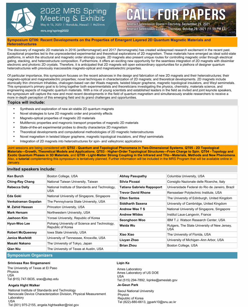
Topics will include:
Invited speakers include:
Symposium Organizers
Ken Burch Boston College, USAChing-Ray Chang National Taiwan University, TaiwanRebecca Dally National Institute of Standards and Technology,
USAEda Goki National University of Singapore, SingaporeVenkatraman Gopalan The Pennsylvania State University, USAM. Zahid Hassan Princeton University, USAMark Hersam Northwestern University, USAJaehoon Kim Yonsei University, Republic of KoreaHyun-Woo Lee Pohang University of Science and Technology,
Republic of KoreaRobert McQueeney Iowa State University, USAJanice Musfeldt University of Tennessee, Knoxville, USAMasaki Nakano The University of Tokyo, JapanQian Niu The University of Texas at Austin, USA
Srinivasa Rao SingamaneniThe University of Texas at El Paso PhysicsUSATel (915) 747-5635, [email protected]
Liqin Ke
Ames Laboratory Ames Laboratory of US DOEUSATel (515) 294-7892, [email protected]
• Synthesis and exploration of new air-stable 2D quantum magnets• Novel strategies to tune 2D magnetic order and proximity effects• Magneto-optical properties of magnetic 2D materials• Multiferroic properties and magnonic transport properties of magnetic 2D materials• State-of-the-art experimental probes to directly characterize 2D magnetism• Theoretical developments and computational methodologies of 2D magnetic heterostructures• Novel magnetism in twisted bilayer graphene, magnetic topological insulators, and Weyl semimetals• Integration of 2D magnets into heterostructures for spin- and valleytronic applications
Abhay Pasupathy Columbia University, USASilvia Picozzi Consiglio Nazionale delle Ricerche, ItalyTatiana Gabriela Rappoport Universidade Federal do Rio de Janeiro, BrazilTrevor David Rhone Rensselaer Polytechnic Institute, USAElton Santos The University of Edinburgh, United KingdomSiddharth Saxena University of Cambridge, United KingdomAndrew Wee T S National University of Singapore, SingaporeAndrew Wildes Institut Laue-Langevin, FranceSeonghoon Woo IBM T.J. Watson Research Center, USAWeida Wu Rutgers, The State University of New Jersey,
USAXiao Xiao The University of Florida, USALiuyan Zhao University of Michigan–Ann Arbor, USABrian Zhou Boston College, USA
The discovery of magnetic 2D materials in 2016 (antiferromagnet) and 2017 (ferromagnets) has created widespread research excitement in the recent past. Exceptional properties led to the unprecedented experimental and theoretical explorations of 2D magnetism. These materials have emerged as ideal solid-state platforms, in which the structural and magnetic order strongly couple. 2D magnets also present unique routes for controlling magnetic order through electrical gating, stacking, and heterostructure composition. Furthermore, it offers an exciting new opportunity for the seamless integration of 2D magnets with dissimilar electronic and photonic 2D crystals. Therefore, it is anticipated that 2D magnets will open extraordinary opportunities for a plethora of designer quantum heterostructures with previously inaccessible magneto-optical and magnetoelectric properties.
Of particular importance, this symposium focuses on the recent advances in the design and fabrication of new 2D magnets and their heterostructures; their magneto-optical and magnetoelectric properties; novel techniques in characterization of 2D magnets; and theoretical developments. 2D magnets include atomically thin chromium trihalides, chalcogen-based van der Waals magnets, twisted bilayer graphene, magnetic topological insulators, and Weyl semimetals. This symposium's primary goal is to bring together both experimentalists and theoreticians investigating the physics, chemistry, materials science, and engineering aspects of magnetic quantum materials. With a mix of young scientists and established leaders in the field as invited and joint keynote speakers, the symposium will capture the new and most recent developments in the field of quantum magnetism and simultaneously enable researchers to receive a more in-depth perception of this emerging field and its grand challenges and opportunities.
Symposium QT06: Recent Developments on the Properties of Emergent Layered 2D Quantum Magnetic Materials and Heterostructures
Joint sessions are being considered with QT02 - Quantum and Topological Phenomena in Two-Dimensional Systems, QT05 - 2D Topological Materials—Growth, Theoretical Models and Applications, QT03 - Higher-Order Topological Structures—From Charge to Spin, QT04 - Topology and Exotic Quantum Phases in 3D Materials, and QT09 - Light-Matter Strong Coupling in the Infrared and THz—Materials, Methods and New Phenomena.Also, a tutorial complementing this symposium is tentatively planned. Further information will be included in the MRS Program that will be available online in January.
Angela Hight WalkerNational Institute of Standards and Technology Nanoscale Device Characterization Division, Physical Measurement LaboratoryUSATel (301) 975-2155, [email protected]
Je-Geun Park
Seoul National University PhysicsRepublic of KoreaTel (822)-880-6613, [email protected]

Topics will include:
Invited speakers include:
Symposium Organizers
Igor Aharonovich University of Technology Sydney, AustraliaDavid Awschalom The University of Chicago, USANathalie de Leon Princeton University, USAJennifer Dionne Stanford University, USASudipta Dubey Indian Institute of Technology Kanpur, IndiaDanna Freedman Northwestern University, USAKai-Mei Fu University of Washington, USAAdam Gali Wigner Research Centre for Physics, HungaryGiulia Galli The University of Chicago, USA
Andre SchleifeUniversity of Illinois at Urbana-Champaign Department of Materials Science and EngineeringUSATel (217) 244-0339, [email protected]
Chitraleema ChakrabortyUniversity of Delaware Department of Materials Science and EngineeringUSATel (302) 831-3251, [email protected]
Jeffrey McCallum
The University of Melbourne School of PhysicsAustraliaTel 61-3-8344-8072, [email protected]
Bruno Schuler
Empa–Swiss Federal Laboratories for Materials Science and TechnologySwitzerlandTel 41-58-765-4929, [email protected]
• Materials synthesis and characterization• Semiconductors, insulators, wide-band-gap materials• Low-dimensional materials• Computational and theoretical modeling• Defect manipulation• Hybrid quantum devices• Identification and control of sources of decoherence• Characterization and modeling of qubits and single-photon emitters
Weibo Gao Nanyang Technological University, SingaporeAndreas Heinrich Center for Quantum Nanoscience, Republic of
KoreaStephen Jesse Oak Ridge National Laboratory, USAUte Kaiser Universität Ulm, GermanyPrineha Narang Harvard University, USAKasturi Saha Indian Institute of Technology Bombay, IndiaMichelle Simmons University of New South Wales, AustraliaNick Vamivakas University of Rochester, USAChris G. Van de Walle University of California, Santa Barbara, USA
Single atom impurities and point defects in solid and molecular semiconductors and insulators have been observed to be excellent quantum systems that behave as qubits or single photon emitters. They can have long lived spin degrees of freedom suitable for quantum information processing, optical transitions that allow for coupling to photons, and promise to push quantum technologies beyond cryogenic environments. These properties spurred intense global interest in further developing such quantum defects as qubits, quantum memories, quantum registers, and single photon sources. However, the intrinsic fragility of quantum states poses a major materials science challenge and building a device that utilizes quantum states requires attention to decoherence-causing defects. For example, qubits based on shallow donors in silicon require close proximity to dielectric interfaces and metal gates to enable control, but can lead to loss of quantum information, rendering defect minimization important. Optical applications of quantum defects require integration into nanophotonic devices, introducing microfabricated surfaces that can host defects that lead to magnetic and electric field noise. In superconducting qubits, defects can act as two-level systems that cause dielectric loss and decoherence. These problems can be circumvented by learning to diagnose and control surfaces and interfaces, and by designing qubits that are insensitive to such issues. Enhanced understanding of defect measurements, manipulation, and modeling is essential but still lacking: Being able to control defects and impurities at the single emitter level and, or even knowing what the defect is, creates challenges that need to be addressed before significant progress can be made, motivating this symposium.
Challenges related to the controlled synthesis of impurities with desired defect spacing and defect type, occur e.g. for diamond or silicon carbide hosts, and low-dimensional materials, such as single-layer boron nitride. In particular, quantum sensing and quantum optics require specific defects in high-quality hosts. Nitrogen-vacancy centers in diamond, for example, can be synthesized using ultrashort laser pulses, but the role of electronic excitations and non-adiabatic mechanisms versus lattice annealing remains an open question. Similarly, techniques for positioning arrays of rare-earth ions in oxides need further development. Challenges for characterization include charge and spin states of defects, to assess suitability as single photon quantum emitters or qubits with long-term stability of their spin excitations. Modeling coupling between quantum defects poses challenges in its own right: Accurately understanding real-time dynamics, electronic and spin excited-state lifetimes, and non-adiabatic electron-ion effects complicates the description, hampering a connection to experiment.
Symposium QT07: Atomic and Molecular Quantum Systems and Defect Engineering for Quantum Technologies

Topics will include:
Invited speakers include:
Symposium Organizers
Marco Abbarchi University Aix-Marseille 3, FranceGerald Buller Heriot-Watt University, United KingdomStefano Chesi Beijing Computational Science Research
Center, ChinaAnais Dreau Université de Montpellier, FranceEva Dupont-Ferrier Université de Sherbrooke, CanadaMark A. Eriksson University of Wisconsin–Madison, USA
Oussama MoutanabbirPolytechnique Montréal Department of Engineering PhysicsCanadaTel (514) 340-4711, [email protected]
Susan CoppersmithUniversity of New South WalesAustraliaTel 61-2-9385-5311, [email protected]
Douglas Paul
University of GlasgowUnited KingdomTel 0000000000, [email protected]
Giordano Scappucci
Delft University of TechnologyNetherlandsTel 31-15-27-85609, [email protected]
• Two-dimensional hole and electron gases.• Quantum dots and Quantum wires.• Single atom doping.• Isotopically enriched semiconductors.• Topological insulators.• Single-photon emitters.• Single-photon detectors.• Spin injection and spin devices.• Photon-to-spin conversion.• Ultrasensitive micro- and nano-electromechanical systems.• Scalable quantum photonics and topological quantum photonics.• Quantum communication and quantum computation.• Quantum sensing and metrology.• Topological quantum computation.• Modeling and packaging.
Elham Fadaly Eindhoven University of Technology, Netherlands
Yvonne Gao National University of Singapore, SingaporeAndrea Hofmann Institute of Science and Technology Austria,
AustriaAngela Kou University of Illinois at Urbana-Champaign, USAHolly Stemp University of New South Wales, AustraliaMenno Veldhorst Delft University of Technology, Netherlands
Uncovering and harnessing quantum phenomena in materials that can leverage industrial semiconductor manufacturing is a long-sought-after strategy to create novel or superior quantum technologies for computing, communication, and sensing. With this perspective, this symposium will bring together a diverse set of scientific communities to present and discuss the progress, current challenges, and future opportunities in group IV quantum engineered materials for integrated quantum technologies. The symposium will cover the broad spectrum from fundamental materials and quantum science to engineering and industrial applications. The first part of the symposium will be dedicated to quantum systems based on group IV materials that are readily integrated on a Si wafer (Si, SiC, Ge, Sn, and their alloys) and their use as platforms to tailor and tune key quantum processes and particles (fermions, Majorana fermions, bosons, anyons, etc.). This includes two-dimensional electron and hole gases, quantum dots, quantum wires, metal-oxide-semiconductor structures, atomic-level doped semiconductors, topological insulators, hybrid superconductor-semiconductor systems, isotopically programmed semiconductors, defect-enabled optical emitters, and ultrasensitive micro- and nano-electromechanical systems (MEMS/NEMS). The key focus will be on the significant progress in materials to solve outstanding challenges in generating, controlling, and manipulating quantum states and quasi-particles. The second part of the symposium will target group IV-enabled quantum components such as qubits, single-photon emitters, single-photon detectors, quantum repeaters, quantum transducers, quantum LIDAR, gravitometers, nanoscale magnetic sensors, etc. Special sessions will be dedicated to focused topics on ultrasensitive metrology, theoretical modeling, quantum device packaging, and challenges in industry-compatible quantum manufacturing.
Abstracts will be solicited in the following areas: Scalable and CMOS-compatible quantum materials and devices; Group IV elements and alloys; Silicon-integrated quantum technologies; Qubits; Single-photon emitters; Single-photon detectors; Ultrasensitive MEMS and NEMS; Spin-photon interfaces; Quantum photonics; Quantum communication; Quantum computing; Quantum sensing.
Symposium QT08: Group IV Quantum Engineering
Joint sessions are being considered with QT07 - Atomic and Molecular Quantum Systems and Defect Engineering for Quantum Technologies.

Topics will include:
Invited speakers include:
Symposium Organizers
Claudia Climent Universsidad Autonoma de Madrid, SpainSimone De Liberato University of Southampton, United KingdomHui Deng University of Michigan, USAFelipe Herrera Universidad de Santiago de Chile, ChileVinod Menon The City University of New York, USA
Thomas Graeme FollandThe University of Iowa Department of Physics and AstronomyUSATel (319) 467-3137, [email protected]
Hatice AltugÉcole Polytechnique Fédérale de Lausanne STI IBI-STI BIOSSwitzerlandTel 41-21-693-11-70, [email protected]
Lauren Buchanan
Vanderbilt University ChemistryUSATel (615) 875-8893, [email protected]
Joshua David Caldwell
Vanderbilt University Mechanical EngineeringUSATel (615) 322-0677, [email protected]
• Spectroscopic techniques for observation of strong coupling in the infrared• Vibrational strong coupling• Polariton-phonon strong coupling• Exciton polaritons• Nonlinear spectroscopy of strongly coupled systems• Strong coupling for biological, biochemical and molecular systems• Ultrafast spectroscopy of strong coupling aspects in chemistry• Novel material systems for strong coupling
Sang-Hyun Oh University of Minnesota, USAMeera Parish Monash University, AustraliaStephanie Reich Freie Universitat Berlin, GermanyBlake Simpkins U.S. Naval Research Laboratory, USAJoel Yuen-Zhou University of California, San Diego, USA
This symposium addresses the reinvigorated topic of strong coupling between light and matter in the infrared and THz spectral ranges (frequency range 1-300 THz), including the emergence of novel quantum interactions. In the strong coupling regime, two or more modes coherently interact and exchange energy at a rate much faster than the energy decay in either material. Under these conditions, the modes take on a hybrid character with properties and information shared between the constituent components. Thus, strong coupling can enable one system to adopt the beneficial properties of another. As such, strong coupling promises advances in quantum optics, control of chemical and biological reaction pathways, and, tailoring of emission properties of infrared emitters.
Strong coupling has been demonstrated in a wide range of materials (including two-dimensional materials, metamaterials, and biological and molecular systems). At its heart, strong coupling relies heavily upon the material properties that can couple to light, and thus investigations of strong coupling require the development of a concerted materials-centric understanding of light-matter interactions. Currently, however, strong coupling phenomena are viewed as interesting phenomenon observed within a variety of research fields, limiting cross-pollination of ideas and concepts between different research communities. It is the intent of this symposium to bring together leaders in strong coupling research across research disciplines. We hope a unified approach will allow us to advance our fundamental understanding of the transition from weak to ultra-strong coupling and from classical to quantum behavior, among other topics.
Symposium QT09: Light-Matter Strong Coupling in the Infrared and THz—Materials, Methods and New Phenomena
A tutorial complementing this symposium is tentatively planned. Further information will be included in the MRS Program that will be available online in January.

Topics will include:
Invited speakers include:
Symposium Organizers
Andrei Bernevig Princeton University, USACory Dean Columbia University, USAFrancisco Guinea IMDEA Materials Institute, SpainShalal Ilani Weizmann Institute of Science, IsraelPablo Jarillo-Herrero Massachusetts Institute of Technology, USAPhilip Kim Harvard University, USAChunNing Jeanie Lau The Ohio State University, USAAllan MacDonald The University of Texas at Austin, USA
Giulia PacchioniSpringerNatureUnited KingdomTel 44-(0)20-7843-4722, [email protected]
Dmitri EfetovInstitut de Ciències FotòniquesSpainTel 34-935542235, [email protected]
Jia Leo Li
Brown University Department of PhysicsUSATel (401) 863-9689, [email protected]
Matthew Yankowitz
University of Washington Department of Physics, Department of Materials Science and EngineeringUSATel (206) 543-1685, [email protected]
• Superconductivity in moiré materials• Magnetism in moiré materials• Ferroelectricity in moiré materials• Topological properties of moiré flat bands• Optical properties of moiré materials• Moiré materials as quantum simulators• Scanning probe imaging and characterization of moiré materials• Development of new experimental control knobs (including in situ twist angle control, strain, and pressure)
Jie Shan Cornell University, USAAshvin Vishwanath Harvard University, USAFeng Wang University of California, Berkeley, USAXiaodong Xu University of Washington, USAAli Yazdani Princeton University, USAAndrea Young University of California, Santa Barbara, USAMike Zaletel University of California, Berkeley, USAEli Zeldov Weizmann Institute of Science, Israel
Moiré materials have recently emerged as widely tunable platforms hosting exotic strongly correlated and topological phenomena, including superconductivity, correlated insulator states, orbital magnetism and ferroelectricity. They can also be used to perform quantum simulation of important models in condensed matter systems. The number of materials that have been combined into moiré structures is continuously growing, currently including graphene, hexagonal boron nitride and transition metal dichalcogenides, with future prospects for expanding to 2D magnets, superconductors, and more. From an initial focus on bilayer structures, the field is now expanding to include the exploration of various types of multilayer moiré materials.
The plethora of phenomena that have been discovered in moiré systems is motivating intense research efforts ranging from understanding the origin of the unconventional superconductivity observed in magic-angle twisted bilayer graphene to investigating the interplay of correlations, magnetism, and topology in a tunable flat-band platform. The increasing number of moiré materials being studied and the richness of emerging new phenomena make this one of the most rapidly evolving fields in condensed matter physics.
This symposium will focus on both experimental and theoretical efforts to understand and characterize phenomena arising in moiré materials, covering the different directions the field is taking, including transport and scanning tunnelling microscopy studies, optical characterization, investigation of magnetic phenomena, efforts to improve fabrication strategies to solve the issue of twist-angle disorder, and the use of moiré materials as quantum simulators.
Symposium QT10: Emerging Phenomena in Moiré Materials
Joint sessions are being considered with QT02 - Quantum and Topological Phenomena in Two-Dimensional Systems.

Topics will include:
Invited speakers include:
Symposium Organizers
Giuseppe Celentano Italian National Agency for New Technologies, Energy and Sustainable Economic Development, Italy
Chang-beom Eom University of Wisconsin–Madison, USAArno Godeke Varian Medical Systems, Inc., GermanyFrancesco Grilli Karlsruhe Institute of Technology, GermanyGaia Grimaldi Consiglio Nazionale delle Ricerche, ItalyRamesh Gupta Brookhaven National Laboratory, USAAlex Gurevich Old Dominion University, USAJens Haenisch Karlsruhe Institute of Technology, GermanyTomoya Horide Kyushu Institute of Technology, JapanHarold Y. Hwang Stanford University, USAIrene Lucas del Pozo University of Zaragoza, Spain
Paolo MeleShibaura Institute of Technology College of Engineering and Innovative Global ProgramJapanTel 81-3-5859-9710, [email protected]
Valeria BracciniConsiglio Nazionale delle RicercheItalyTel 390106598722, [email protected]
Kazumasa Iida
Nagoya University Department of Materials PhysicsJapanTel 81-52-789-3853, [email protected]
Qiang Li
Brookhaven National LaboratoryUSATel (631) 344-4490, [email protected]
• Superconducting qubits: materials issues, gates and error corrections• Josephson junctions technology and interface• Topological superconductors and unconventional superconductivity• REBCO wires and Coated Conductors: processing and applications• Fe-based superconductors and potential applications• Bi-based, Nb-based, MgB(2) tapes and round wires: processing and applications• Flux pinning and critical currents: intrinsic pinning behavior, anisotropy, irradiation effect• Energy applications and devices based on superconducting materials
Andrea Malagoli Consiglio Nazionale delle Ricerche, ItalyMasashi Miura Seikei University, JapanToshinori Ozaki Kwansei Gakuin University, JapanAnna Palau Institut de Ciència de Materials de Barcelona,
SpainJeong Ming (Jane) Park Massachusetts Institute of Technology, USAMarty Rupich American Superconductors, USATakao Sasakawa Tokyo Institute of Technology, JapanSusannah Speller University of Oxford, United KingdomTsuyoshi Tamegai The University of Tokyo, JapanAkiyasu Yamamoto Tokyo University of Agriculture and Technology,
Japan
The symposium will broadly cover superconducting materials and applications. An emphasis is placed on facilitating the transition from basic science discoveries to technology deployment of superconducting materials. Contributions to the development of novel and customized superconducting materials are encouraged, which include superconducting electronics for quantum computation and large-scale superconducting devices for high field magnets and power applications.
The superconducting materials of interests include conventional low-temperature superconductors for electronics and sensors, intermetallic superconductors (Nb-Ti and Nb3Sn), medium- and high-temperature superconductors (cuprates, iron-based compounds, and MgB2), superconducting multi-layers and composites, the recently discovered room-temperature hydride superconductors and other emergent materials exhibiting unconventional superconductivity like topological superconductors. Symposium contributors in the area of materials are encouraged to address issues including: 1) response of superconductivity to structural, chemical, and defect tuning; 2) improvement of existing practical materials; 3) synthesis, growth mechanisms, and high throughput fabrication routes; 4) methods to improve application-relevant properties such as flux pinning.
Symposium QT11: Superconducting Materials and Applications
A tutorial complementing this symposium is tentatively planned. Further information will be included in the MRS Program that will be available online in January.

Topics will include:
Invited speakers include:
Symposium Organizers
Derya Baran King Abdullah University of Science and Technology, Saudi Arabia
Mariano Campoy-Quiles Nanostructured Materials for Optoelectronics and Energy Harvesting, Spain
Michael Chabinyc University of California, Santa Barbara, USACarsten Deibel Technische Universität Chemnitz, GermanyChong-an Di Institute of Chemistry, Chinese Academy of
Sciences, ChinaYing Diao University of Illinois at Urbana-Champaign, USALei Fang Texas A&M University, USAAlessio Gagliardi Technische Univeristät München, GermanyDavid Ginger University of Washington, USAWenping Hu Tianjin University, ChinaLynn Loo Princeton University, USAChristine Luscombe Okinawa Institute of Science and Technology,
JapanIain McCulloch Oxford University, United Kingdom
Xiaodan GuThe University of Southern MississippiUSATel (601) 266-5646, [email protected]
Brian A. CollinsWashington State UniversityUSATel (509) 335-4671, [email protected]
Eva M. Herzig
Universität BayreuthGermanyTel +49(0)921-55-2619, [email protected]
Ting Lei
Peking University School of Materials Science and EngineeringChinaTel +86-18612088927, [email protected]
• In situ/operando characterization of organic and hybrid materials• Frontiers in multimodal nanostructure measurements involving electrons, X-rays, neutrons, and scanning probes• Merging experiment with theory and simulation towards designed materials, structures, and properties• Novel algorithms, machine learning, and other approaches towards predictive methods of structure and properties• Engineering interfacial and bulk structures to influence excited state dynamics and performance• Understanding of the structure and dynamics of conjugated polymers for stable device operation• Holistic design of molecules to address device processing, structure, properties, and lifetime• Emerging device applications that harness the advantages of organic materials
Jianguo Mei Purdue University, USAMarcus Noack Lawrence Berkeley National Laboratory, USAHarald Oberhofer Technical University of Munich, GermanyJian Pei Peking University, ChinaLillo Pozzo University of Washington, USAErin Ratcliff University of Arizona, USAJonathan Rivnay Northwestern University, USASimon Rondeau-Gagné University of Windsor, CanadaBret Savoie Purdue University, USANatalie Stingelin Georgia Institute of Technology, USAWei You University of North Carolina at Chapel Hill, USAYingping Zou Central South University, China
The potential of next-generation flexible, printable, and biocompatible electronic devices made from organic materials continues to draw significant interest in the research community. This symposium focuses on how the community can realize this potential through advanced nanostructure characterization and device physics combined with state-of-the-art computational methods to enable breakthroughs in design of molecular materials. Recent results show exciting new high-performance devices within innovative application spaces. Of particular interest are novel in-situ or operando experimental studies that reveal the dynamics of film formation into a final organic or hybrid nanostructure in connection to resulting properties and performance. In addition, studies are called for which involve new computational techniques and algorithms that can predict the statistically relevant structure and properties as well as intelligently fuse such results with multimodal quantitative measurements. Finally, the emphasis is given to combining such experimental and computational insights to drive the design of the next generation materials and devices.
Symposium SB01: Organic Electronics—Multimodal Characterization and Computation-Driven Material Design and Performance

Topics will include:
Invited speakers include:
Symposium Organizers
Ichiro Amimori Xenoma Inc., JapanYi Cui Stanford University, USAMarco Fontana Sant’Anna School of Advanced Studies, ItalyChuafei Guo Southern University of Science and Technology,
ChinaChristoph Keplinger Max Planck Institute for Intelligent Systems,
GermanyDae-Hyeong Kim Seoul National University, Republic of KoreaCecilia Laschi National University of Singapore, SingaporePooi See Lee Nanyang Technological University, SingaporeYigit Menguc Facebook Reality Labs, USA
Kenjiro FukudaRIKENJapanTel 81-48-467-9174, [email protected]
Vito CacuccioloÉcole Polytechnique Fédérale de LausanneSwitzerlandTel +41 216954106, [email protected]
Shingo Maeda
Shibaura Institute of TechnologyJapanTel 81-3-5859-8062, [email protected]
Xiaomin Xu
Tsinghua University Tsinghua-Berkeley Shenzhen InstituteChinaTel 86-755-36881552, [email protected]
• Thin and light-weight energy harvesting/storage devices• Stretchable conductors• Soft actuators for untethered robots and wearables• Soft robotics and artificial intelligence with a focus on untethered systems• Design & materials for Flexible and stretchable electronic devices• Organic and hybrid electronics for flexible/stretchable devices• Soft optical devices for imaging, sensing and stimulation• Integrated systems for soft-robot applications
Kohei Nakajima The University of Tokyo, JapanJohn Rogers Northwestern University, USAHerbert Shea École Polytechnique Fédérale de Lausanne,
SwitzerlandTakao Someya The University of Tokyo, JapanKenji Suzuki University of Tsukuba, JapanKoichi Suzumori Tokyo Institute of Technology, JapanKuniharu Takei Osaka Prefecture University, JapanZhong Lin Wang Georgia Institute of Technology, USA
In recent years, considerable efforts have been devoted to developing novel soft robots, yielding advances in biomimetic robot mechanisms, soft actuators, soft artificial organs, and biocompatible and conformable prostheses. To realize these applications, high-performance power sources, sensors, actuators, and processors made of soft materials are essential.
The final step to achieve wearable and autonomous soft robots is to remove their tether to electrical power and introduce untethered systems. The integration of new, flexible energy harvesting/storage devices with soft actuators and sensors makes it possible to achieve this ultimate form of soft robots. For further development and future practical applications, multidisciplinary research linking materials, devices, actuation, mechanics, and information processing is critical. Based on this motivation, the main purpose of this symposium, by gathering researchers from different disciplines worldwide, is to discuss the challenges and possibilities for the next generation of soft robots. This symposium will cover newly developed materials, thin and light-weight energy harvesting/storage devices, flexible/stretchable sensors, flexible photonics for sensing and stimulation, new mechanics, and artificial intelligence.
Thanks to their tissue-like mechanical compliance (including both flexibility and stretchability), devices built with soft materials can serve as the interface between the electronic world and the biological one, conforming to internal organs or skin and other soft, curved surfaces. Furthermore, the stretchability of these devices allows them to maintain operation even under large deformation. Already, soft robots and soft machines that integrate energy harvesting, sensing, actuation, and information processing have appeared, heralding remarkable potential applications in wearable consumer electronics, mobile health monitoring, artificial prostheses, artificial organs, and disaster relief.
Symposium SB02: Materials, Power Sources, Sensors, Actuators and Mechanics for Untethered Soft Robots
Joint sessions are being considered with SB08 - Soft Embodiments of Electronics and Devices for Healthcare Applications.

Topics will include:
Invited speakers include:
Symposium Organizers
Bilge Baytekin Bilkent University, TurkeyRavinder Dahiya University of Glasgow, United KingdomChiara Daraio California Institute of Technology, USAKristen Dorsey Smith College, USARyan Hayward University of Colorado Boulder, USAYan Ji Tsinghua University, ChinaMirko Kovac Imperial College London, United KingdomRebecca Kramer-Bottiglio
Yale University, USA
Andreas Lendlein University of Potsdam, Germany
Ryan TrubyNorthwestern University Materials Science and Engineering, Mechanical EngineeringUSATel (432) 770-4103, [email protected]
Mihai DudutaUniversity of Toronto Mechanical and Industrial EngineeringCanadaTel (416) 978-3040, [email protected]
Barbara Mazzolai
Istituto Italiano di Tecnologia Center for Micro-BioRoboticsItalyTel 39-050-883444, [email protected]
Huichan Zhao
Tsinghua University Mechanical EngineeringChinaTel 86-10-62771279, [email protected]
• Actuators for soft robots and devices - liquid crystal elastomers, dielectric elastomer actuators, and shape-memory/shape-morphing materials• Elastomers, hydrogels, polymers, and composites for robot bodies• Materials and strategies for power and energy management in soft devices• Additive and digital fabrication schemes for soft robots and robotic materials• Architected and biomimetic materials for robots• Materials for self-healing, growing, learning, and other adaptive robotic functions• Bioinspired and biohybrid design in robotic materials• Modeling, simulation, and control of robotic materials• Robotic materials for innovations at the human-robot interface• Autonomous soft/microscale robots and active matter
Hani Naguib University of Toronto, CanadaJordan Raney University of Pennsylvania, USAHerbert Shea École Polytechnique Fédérale de Lausanne,
SwitzerlandRobert Shepherd Cornell University, USAMetin Sitti Max Planck Institute for Intelligent Systems,
GermanyThomas Speck Albert-Ludwigs-Universität Freiburg, GermanyZeynep Temel Carnegie Mellon University, USALi Zhang The Chinese University of Hong Kong, China
The natural world motivates a new paradigm for robot design: advancing machine intelligence by way of new materials for robot bodies, whose mechanical and physicochemical properties yield advanced capabilities and autonomous behaviors akin to those of living organisms. Soft robotics has exemplified how a materials-driven approach to robotics has expanded robots’ abilities, opened new avenues for wearable and biomedical machines, and transformed our ideas of what a robot is and can be. However, continued advances are needed to address fundamental limitations in fabrication, power, and control. To address these interdisciplinary challenges, this symposium will bring together researchers from soft and microscale robotics, stretchable electronics, active matter, mechanics, and chemistry to share research that advances robotics by way of new materials.
This symposium is structured around three research themes. The first theme - robotic components from soft and architected materials - will feature new materials for actuation, perception, power, and control capabilities in soft robots and devices across all scales. Innovations of special interest include electrically-driven soft actuators, self-powered components, chemical power strategies, and iontronic devices. The second theme - integrated design and fabrication strategies for robotic materials - will showcase progress in manufacturing. Methods of particular interest will facilitate distributed actuation and sensing capabilities, multi-material fabrication, multiscale assembly, and/or paths towards the end-to-end design, fabrication, and evaluation of robotic materials. The third theme - advances in the modeling and control of materials for physical machine intelligence - will highlight theoretical contributions that will improve robotic material design and fabrication. The symposium will broadly explore new applications for robotic materials, including autonomous/untethered systems, wearable and biomedical devices, smart textiles, and beyond.
Symposium SB03: Robotic Materials for Advanced Machine Intelligence
Joint sessions are being considered with SF13 - From Actuators and Energy Harvesting Storage Systems to Living Machines.

Topics will include:
Invited speakers include:
Symposium Organizers
Polina Anikeeva Massachusetts Institute of Technology, USAChris Bettinger Carnegie Mellon University, USAMary Donahue Linköping University, SwedenKenjiro Fukuda RIKEN, JapanWei Gao California Institute of Technology, USAAnna Herland KTH Royal Institute of Technology, SwedenSuk-Won Hwang Korea University, Republic of KoreaAli Javey University of California, Berkeley, USAUnyong Jeong Pohang University of Science and Technology,
Republic of KoreaPawan Jolly Harvard University, USAMartin Kaltenbrunner Johannes Kepler Universität Linz, AustriaShana Kelley University of Toronto, Canada
Myung-Han YoonGwangju Institute of Science and Technology School of Materials Science and EngineeringRepublic of KoreaTel 82-10-6226-9026, [email protected]
Michael DickeyNorth Carolina State University Department of Chemical and Biomolecular EngineeringUSATel (919) 513-0273, [email protected]
Sahika Inal
King Abdullah University of Science and Technology Biological and Environmental Science and Engineering DivisionSaudi ArabiaTel 390223999875, [email protected]
Hyunhyub Ko
Ulsan National Institute of Science and Technology School of Energy and Chemical EngineeringRepublic of KoreaTel 82-52-217-2532, [email protected]
• Flexible and/or stretchable active/passive materials for bioelectronics• Conductive hydrogel materials• Self-healing, biocompatible, and biodegradable soft electronic materials• Soft conductive materials for 3D printing• Soft organic, inorganic, or hybrid materials with capacitive, piezoelectric, piezoresistive, triboelectric, and/or ferroelectric properties• Stimuli (e.g., stress, light, heat, pH, chemical, etc.)-responsive soft materials• Soft electronic materials for biochemical sensing• Soft electronic materials for electrocardiogram (ECG or EKG), electroencephalogram (EEG), electromyogram (EMG), and electrooculogram (EOG)• Novel electronic materials for brain-machine interfaces• Novel stretchable and/or flexible device architectures for practical applications in the fields of healthcare, robotics, sports, IoTs, etc.• Soft energy harvesting materials for bioelectronics
Dae-Hyeong Kim Seoul National University, Republic of KoreaSang-Woo Kim Sungkyunkwan University, Republic of KoreaStéphanie P. Lacour École Polytechnique Fédérale de Lausanne,
SwitzerlandHyunjoo Lee Korea Advanced Institute of Science and
Technology, Republic of KoreaWei Lin Leong Nanyang Technological University, SingaporeChristian Müller Chalmers University of Technology, SwedenClara Santato Polytechnique Montréal, CanadaThomas Stieglitz Universität Freiburg, GermanyJeong-Yun Sun Seoul National University, Republic of KoreaBenjamin Tee National University of Singapore, SingaporeJadranka Travas-Sejdic University of Auckland, New ZealandSheng Xu University of California, San Diego, USA
Bioelectronic interfaces, which facilitate the transduction of biological signals and the stimulation of biological organs/tissues, open new opportunities for various applications such as healthcare, robotics, sports, and e-games. These devices often require the conformal attachment of devices on the curvilinear human skin or organ surface and the long-term operational reliability even under severe mechanical deformation.For these purposes, many researchers have been searching for specialized constituent materials, particularly, targeting stretchable/flexible/soft conductors, semiconductors, and dielectrics, in conjunction with processing/integration methods toward robust high-performance devices.
This symposium covers the recent progress in advanced soft materials, processing, and device architectures for bio-electronic interfaces in the fields of healthcare, robotics, sports, and Internet of Things (IoTs), etc.
Symposium SB04: Advanced Soft Materials for Bioelectronic Interfaces
Joint sessions are being considered with SB05 - Tissue-Like Bioelectronics and Living Bioelectronic Interfaces, and SB06 - Bioelectronic Materials and Devices for In Vitro Systems.

Topics will include:
Invited speakers include:
Symposium Organizers
Tzahi Cohen-Karni Carnegie Mellon University, USATal Dvir Tel Aviv University, IsraelYing Fang National Center for Nanoscience and
Technology, ChinaDiego Ghezzi École Polytechnique Fédérale de Lausanne,
SwitzerlandSahika Inal King Abdullah University of Science and
Technology, Saudi ArabiaAbigail Koppes Northeastern University, USAKristen Kozielski Karlsruhe Institute of Technology, GermanyDuygu Kuzum University of California, San Diego, USAAntonio Lauto Western Sydney University, Australia
Alexandra RutzWashington University in St. LouisUSATel 3149352348, [email protected]
Stéphanie P. LacourÉcole Polytechnique Fédérale de LausanneSwitzerlandTel 41-21-693-11-81, [email protected]
Damia Mawad
University of New South WalesAustraliaTel 61293856642, [email protected]
Jacob T. Robinson
Rice UniversityUSATel (713) 348-2933, [email protected]
• Conducting hydrogels & proteins• Bioelectronic devices built from soft & hydrated materials• Cell-laden, biohybrid, or tissue-embedded bioelectronic devices• Printed bioelectronics for integration of multiple materials and/or cells• The use of electronics for engineered tissues, for recording or stimulation, such as tissues-on-chips• Material strategies for improving cellular & tissue interfaces with electronics• Biocompatibility studies & chronic evaluations of bioelectronic materials & devices• Chronic evaluations of implanted devices• New materials and material modifications to prolong device functionality/operation in biological environments• Biomimetic bioelectronics• Biofunctional nanomaterials• Materials considerations for bioelectronic data and power transfer
Adam Micolich University of New South Wales, AustraliaIvan Minev The University of Sheffield, United KingdomHidenori Okuzaki University of Yamanashi, JapanRoisin Owens University of Cambridge, United KingdomJonathan Rivnay Northwestern University, USAFrancesca Santoro Istituto Italiano di Tecnologia, ItalyMolly Stevens Imperial College London, United KingdomFlavia Vitale University of Pennsylvania, USA
Bioelectronics are a broad class of devices that convert biological information into electronic currents or vice versa. Such systems give rise to bidirectional flows of information between humans and machines and serve as instrumental therapeutics and diagnostics. Examples include implantable medical devices (e.g. pacemakers, cochlear implants, neural probes), surgical tools, and scientific apparatus. To expand efficacy, utility, and new applications, innovation is needed in the structural and functional properties of bioelectronic devices and the materials that compose these devices. Challenges include improving biological-device interfaces for resolution and specificity and prolonging device operation in biological environments. This symposium will cover the latest innovative materials and fabrication strategies that blur distinctions between tissue and device.
Material advances borrowed from other fields, such as tissue engineering, tissues-on-chip, and neural engineering, are fueling innovation in bioelectronic devices. Advanced manufacturing methods, such as 3D printing and bioprinting, that expand the versatility of materials in device composition and give rise to novel device structures and function will be highlighted. Emerging approaches that integrate biomaterials (e.g. hydrogels, proteins), thin films and devices laden with cells that are incorporated either during or after fabrication will be explored. Basic studies of biological-electrical interfaces, which elucidate important materials and device design principles are also key areas to be covered. The symposium will bring together investigators from a range of disciplines and whose research spans the spectrum of these topics.
Symposium SB05: Tissue-Like Bioelectronics and Living Bioelectronic Interfaces
Joint sessions are being considered with SB06 - Bioelectronic Materials and Devices for In Vitro Systems, and SB08 - Soft Embodiments of Electronics and Devices for Healthcare Applications.

Topics will include:
Invited speakers include:
Symposium Organizers
Craig Aspinwall University of Arizona, AustriaFabio Biscarini University of Modena, ItalyAnnalisa Bonfiglio Università degli Studi di Cagliari, ItalyTzahi Cohen-Carni Carnegie Mellon University, USASahika Inal King Abdullah University of Science and
Technology, Saudi ArabiaSven Ingerbrandt RWTH Aachen University, GermanySungjune Jung Pohang University of Science and Technology,
Republic of KoreaWolfgang Knoll Austrian Institute of Technology, AustriaGeorge Malliaras University of Cambridge, United KingdomDamia Mawad University of New South Wales, Australia
Anna-Maria PappaUniversity of Cambridge Chemical Engineering and BiotechnologyUnited KingdomTel 447547989640, [email protected]
Susan DanielCornell University School of Chemical and Biomolecular EngineeringUSATel (607) 255-4675, [email protected]
Roisin Owens
University of Cambridge Chemical Engineering and BiotechnologyUnited KingdomTel 44-(0)1223-763969, [email protected]
Alberto Salleo
Stanford University Department of Materials Science and EngineeringUSATel (650) 725-2648, [email protected]
• Engineering the cell-material interface• Bioinspired electronic materials and structures• Cell based nanobioelectronics (nanomaterials, nanopatterning etc)• 2D electronic materials and devices or bio-interfacing• 3D bioelectronic models/ devices (including electroactive scaffolds, organoids, spheroids)• On-chip integration of electronics with biological components (organ/tissues on chip, plasma membranes on chip etc)• Interfacing subcellular components (i.e., organelles, vesicles etc) with bioelectronics• Membrane biophysics (ion channel function, nanopore sensing, electrophysiology etc)• Electronic sensors of cellular metabolic activity
Aleksandr Noy Lawrence Livermore National Laboratory, USACharalampos Pitsalidis University of Cambridge, United KingdomAgneta Richter-Dahlfors KTH Royal Institute of Technology, SwedenMarco Rolandi University of California, Santa Cruz, USAKaori Sugihara University of Geneva, SwitzerlandBozhi Tian The University of Chicago, USAFeng Yan The Hong Kong Polytechnic University, Hong
KongMyung-Han Yoon Gwangju Institute of Science and Technology,
Republic of KoreaJenny Zhang University of Cambridge, United Kingdom
In vitro bioelectronics combines the realms of electronics and in vitro biological systems with the aim of developing improved bioassays for drug screening or for fundamental studies. As in the broader field of bioelectronics, progress in this area has been mainly driven by advances in materials science and device engineering as well as by the development of more predictive biological models. Materials that promote communication with cells can result in novel device configurations that can transduce and even amplify biological signals, bridging the gap between biology and measurements towards predictive models that can be reliably used for high-throughput high-content studies.The merging of synthetic biology and bioengineering with electronics allows for precise control over the biological model offering unprecedented opportunities to probe biology at multiple length scales, as well as to use biotechnology approaches to exploit biomolecules for applications such as energy harvesting and environmental/healthcare diagnostics. This symposium will encompass advances in multifunctional electronic materials, for interfacing biology, as well as for satisfying the technological demands of electronics industry such as compatibility with large area processes and miniaturisation. The scope of this symposium will go beyond traditional in vitro cell-based models and include cell-free biological models made via synthetic and bioinspired routes including cell membranes, vesicles and subcellular components.
Symposium SB06: Bioelectronic Materials and Devices for In Vitro Systems
Joint sessions are being considered with SB05 - Tissue-Like Bioelectronics and Living Bioelectronic Interfaces, and SB04 - Advanced Soft Materials for Bioelectronic Interfaces.

Topics will include:
Invited speakers include:
Symposium Organizers
Frank Caruso University of Melbourne, AustraliaLiang Cheng Soochow University, ChinaTomáš Etrych The Czech Academy of Sciences, Czech
RepublicZhen Gu Zhejiang University, ChinaTaeghwan Hyeon Seoul National University, Republic of KoreaShana Kelley University of Toronto, CanadaEster Kwon University of California, San Diego, USATeri Odom Northwestern University, USAKanyi Pu Nanyang Technological University, Singapore
Weibo CaiUniversity of Wisconsin–Madison Radiology, Medical Physics, Materials Science & Engineering, Pharmaceutical SciencesUSATel 01-608-658-0892, [email protected]
Zi (Sophia) GuUniversity of New South Wales School of Chemical EngineeringAustraliaTel -61-(2)-9385-4964, [email protected]
Dawei Jiang
Huazhong University of Science & Technology Nuclear MedicineChinaTel 86-13761401048, [email protected]
Dalong Ni
Shanghai Jiao Tong University School of MedicineChinaTel 86-021-64313534, [email protected]
• Nanotheranostics in response to biological stimuli• Nanotheranostics in response to physical stimuli• Biomimetic nanotheranostics• Clinical translation of nanotheranostics• Nanomaterials for biomedical imaging• Nanomaterials for new type of treatments• Nanomaterials as drug delivery systems
Molly Stevens Imperial College London, United KingdomWei Tao Harvard Medical School, USANguyen Thanh University College London, United KingdomKristopher Thurecht University of Queensland, AustraliaMatthew Tirrell The University of Chicago, USAZhi Ping Xu University of Queensland, AustraliaLiangfang Zhang University of California, San Diego, USAJie Zheng The University of Texas at Dallas, USA
This symposium will cover the vibrant research field of the design and development of novel nanomaterials that can integrate therapeutic (e.g. drug/gene delivery, radiation, thermal/dynamic therapy, etc.) and diagnostic (e.g. non-invasive imaging, in vivo/ex vivo sensing, etc.) capabilities, in response to various cues in the biological/physiological environment (e.g. pH, redox potential, enzyme, glucose, oxygen level, biomimicry, etc.) and/or certain physical stimuli (e.g. temperature, magnetic field, radiation, light, self-assembly/disassembly, etc.).
Despite significant advances in medical approaches, many critical questions still remain: How to realize accurate prognosis to guide personalized/precision treatment? How to achieve desirable therapeutic efficacy while minimizing adverse systematic toxicity? How to spatiotemporally monitor drug fate and drug response for precision medicine? By harnessing the modular structure and bioresponsive properties of functional nanomaterials, nanotheranostics hold tremendous potential to provide accurate diagnostic and therapeutic capabilities, which has been a flourishing field of the last decade.
This symposium will gather the brightest minds with academic, industry and clinical backgrounds from many international institutions to share cutting-edge research and inspirational opinions, which will foster/catalyze exciting opportunities for (international) interdisciplinary and multidisciplinary collaborations. With an elite list of internationally renowned invited speakers from several continents, we welcome abstract submissions from all around the world to this exciting forum of scientific exchange.
Symposium SB07: Bioresponsive Nanotheranostics

Topics will include:
Invited speakers include:
Symposium Organizers
Polina Anikeeva Massachusetts Institute of Technology, USAMichael Dickey North Carolina State University, USAEric Glowacki Linköping University, SwedenChristoph Keplinger University of Colorado Boulder, USAStéphanie P. Lacour École Polytechnique Fédérale de Lausanne,
SwitzerlandNanshu Lu The University of Texas at Austin, USAGeorge Malliaras University of Cambridge, United KingdomNicholas Melosh Stanford University, USA
Mary DonahueLinköping University Laboratory of Organic ElectronicsSwedenTel 46-700896461, [email protected]
Martin KaltenbrunnerJohannes Kepler Universität Linz Soft Matter Physics DivisionAustriaTel 43-732-2468-9760, [email protected]
Dion Khodagholy
Columbia University Electrical Engineering School of Engineering and Applied ScienceUSATel (212) 854-1745, [email protected]
Takafumi Uemura
Osaka University The Institute of Scientific and Industrial ResearchJapanTel 06-6879-8400, [email protected]
• Soft embodiments of electronics and prosthetics• Flexible/stretchable electronic materials• Organic multifunctional materials• Organic/inorganic and hybrid materials and systems• Conducting hydrogels• Substrates and encapsulation materials / methods with superior mechanical / thermal properties• Novel signal transduction approaches• Self-healing materials and sensors• Wireless communication integrated with bioelectronic sensors and devices• Biocompatible / bioresorbable layers• Understanding the interface between organic electronics and biological materials• Theory & modelling• Molecular electronics & photonics• Combining multiple sensing or stimulation modalities
John Rogers Northwestern University, USATsuyoshi Sekitani Osaka University, JapanRobert Shepherd Cornell University, USATakao Someya The University of Tokyo, JapanKuniharu Takei Osaka Prefecture University, JapanBenjamin Tee National University of Singapore, SingaporeBozhi Tian The University of Chicago, USA
Advancement in the field of flexible/stretchable electronics, and the materials needed to provide soft embodiments of electronics, is essential to the improvement of devices for healthcare applications. Providing a seamless interface between electronics and the human body is crucial for applications such as rehabilitation, brain machine interfaces, diagnostics, and disease management. Critical factors that drive the widespread introduction of systems aiming to establish a highly functional biological interface include the performance, cost, stability, power management, and lifetime of the materials. This symposium focuses on the development of soft, elastic, and flexible materials, devices and technologies aimed at advancement in healthcare. This includes the fundamental understanding of the material systems and use of these in applications which benefit from the compliant nature of the materials.
Progress within this field relies on multidisciplinary expertise, including electronics, material science, biology, and biophysics. Bringing together scientists and engineers actively engaged in research and development in these fields will facilitate possibilities to overcome limitations of current materials and devices. This will in turn enable further advancement of next-generation materials and devices, resulting in new opportunities in the areas of medicine, healthcare, and brain-machine interactions. The invited speakers possess expertise over a range of material systems as well as the targeted applications. A strong focus of this symposium is to facilitate collaboration between academic institutions and industry.
Symposium SB08: Soft Embodiments of Electronics and Devices for Healthcare Applications
Joint sessions are being considered with SB02 - Materials, Power Sources, Sensors, Actuators and Mechanics for Untethered Soft Robots, and SB05 - Tissue-Like Bioelectronics and Living Bioelectronic Interfaces.Also, a tutorial complementing this symposium is tentatively planned. Further information will be included in the MRS Program that will be available online in January.

Topics will include:
Invited speakers include:
Symposium Organizers
Kristi Anseth University of Colorado Boulder, USADavid Baker University of Washington, USAWeibo Cai University of Wisconsin, USAHongjie Dai Stanford University, USACole DeForest University of Washington, USANicholas Kotov University of Michigan–Ann Arbor, USASteven Little University of Pittsburgh, USAJia Liu Harvard University, USA
Ritchie ChenStanford University BioengineeringUSATel (857) 928-1530, [email protected]
Polina AnikeevaMassachusetts Institute of Technology Materials Science and EngineeringUSATel (617) 258-7348, [email protected]
Ester Kwon
University of California, San Diego BioengineeringUSATel (206) 437-2915, [email protected]
Molly Stevens
Imperial College London Materials and BioengineeringUnited KingdomTel 44-(0)20-7594-6804, [email protected]
• Tissue engineering• In situ tissue chemistry• Organoids, spheroids and multicellular assembly• Biomolecular self-assembly• Nanomaterial-cellular interface• Biorthogonal chemistry• Supramolecular chemistry• Bioelectronics• Nanomedicine• Synthetic Biology
Timothy Lu Massachusetts Institute of Technology, USANikhil Malvankar Yale University, USAMichael Mayer University of Fribourg, SwitzerlandAdrianne Rosales The University of Texas at Austin, USASamuel Stupp Northwestern University, USAJerry Yang University of California, San Diego, USAShu Yang University of Pennsylvania, USALiangfang Zhang University of California, San Diego, USA
Living cells exhibit exquisite control over their molecular networks to detect environmental changes and to execute sophisticated commands. Bio-inspired or bio-integrated engineering of these cellular processes have enabled new avenues to manipulate the form and function of cells and tissue both ex vivo and in vivo. In this symposium, we will actively discuss how the convergence of materials science, synthetic biology, and bioengineering has facilitated the evolution of biomaterials from passive scaffolds to dynamic systems. We will focus on the materials design of bio-inspired, genetically-encoded and biomolecular materials and their application in mimicking and/or understanding living systems as well as in the development of new treatment concepts and therapeutics.
This symposium will be devoted to both fundamental research and applications of bio-inspired and genetically-encoded materials grouped into the following themes: tissue engineering, nanomedicine and bioelectronics. In the first theme on tissue engineering, we will cover topics on bioactive hydrogels, cellular bioprinting, and other materials approaches that incorporate biological matter and/or genetic engineering to assemble complex microenvironments for tissue modeling and regeneration. In the second theme on nanomedicine, we will focus on the molecular assembly of biomolecular (e.g. nucleic acids and proteins), nanoscale (e.g. viruses and exosomes), cellular or synthetic material to enable new therapeutic approaches. Finally, the bioelectronics theme will explore topics that include redox and conductive biomolecules as well as genetically-encoded reporters and actuators of cellular activity. This symposium will highlight multidisciplinary efforts to advance biomaterials research towards new approaches and solutions for precision medicine.
Symposium SB09: Genetically-Encoded and Bioinspired Materials Science

Topics will include:
Invited speakers include:
Symposium Organizers
Elizabetta Collini University of Padova, ItalyUrs Frey MaxWell Biosystems, SwitzerlandDion Khodagholy Columbia University, USADavid Kisailus University of California, Irvine, USAKeon Jae Lee Korea Advanced Institute of Science and
Technology, Republic of KoreaYi-Kuen Lee The Hong Kong University of Science and
Technology, Hong KongJulie Lin Panasonic Singapore, SingaporeKazuki Nagashima The University of Tokyo, Japan
Yoriko TominagaHiroshima UniversityJapanTel 81-82-424-7649, [email protected]
Antal BerenyiUniversity of SzegedHungaryTel 36-62-545-373, [email protected]
Brandon J. Mitchell
West Chester UniversityUSATel (585) 313-8129, [email protected]
Hiroto Sekiguchi
Toyohashi University of TechnologyJapanTel 81-532-44-6744, [email protected]
• Biogenic materials, nanoparticles, and nanostructures• Understanding of mechanisms for biomimetic material synthesis• Electron microscopy and spectroscopy, optical spectroscopy, and in-situ characterization methods, as well as methods to probe biomimetic
functionalities• Nanomaterials and composites for bioelectronics• Implantable bioelectoronic devices• Flexible bio-chips for biomedical science• Light operation technology for optogenetics• Bioimaging technology for observation of life activities• Biosensing devices and techniques for healthcare
Jun Ohta Nara Institute of Science and Technology, JapanYoshiko Okamura Hiroshima University, JapanKazuaki Sawada Toyohashi University of Technology, JapanMicho Suzuki The University of Tokyo, JapanYasuo Terasawa Nidek Co., Ltd., JapanLan Yin Tsinghua University, ChinaEuisik Yoon University of Michigan, USA
Complex-states are interconnected processes that often occur as broader phenomena in emerging fields such as biomimetics and biophotonics. As the mechanisms behind these processes are revealed, or applications of the phenomena are being considered, it becomes necessary to decouple and isolate the individual processes. In materials synthesis using biomineralization, for example, the individual role of the stiffened component inside a cell should be clarified. In disease detection, a single diagnostic biomarker can provide higher disease detection sensitivity than symptomatic diagnosis. For optogenetics, where precise control of neural networks is desired, the off target activation of neurons due to excess heat and biologically active wavelengths of light must be minimized for use in human tissue.
This symposium will cover a variety of topics related to mixed or coupled systems that are common in biomimetic functionalities such as biogenic nanocomposite fabrication, electronic and optical devices for biosensing, and optogenetics. The use of novel or state-of-the-art characterization methods to elucidate the underlying mechanisms behind these functionalities will be an important aspect of the symposium. This symposium aims to bring together a diverse community of researchers in physics, chemistry, biology and engineering who are advancing the field of biomimetic functionality through material synthesis, nanofabrication, and device application. The goal of the symposium is to provide opportunities to discuss complex-states in interdisciplinary phenomena, as well as current challenges that exist and possible approaches for overcoming them.
Symposium SB10: Complex States in the Observation, Control and Utilization of Biomimetic Functionalities—From Fundamentals to Applications

Topics will include:
Invited speakers include:
Symposium Organizers
Benjamin Beeler North Carolina State University, USAColin Boxall Lancaster University, United KingdomMarco Cologna European Commission Joint Research Centre,
GermanyChaitanya Deo Georgia Institute of Technology, USALionel Desgranges Commissariat à l’énergie atomique et aux
énergies alternatives, FranceSarah Finkeldei University of California, Irvine, USAChristine Gueneau Commissariat à l’énergie atomique et aux
énergies alternatives, FranceLingfeng He Idaho National Laboratory, USAPeter Hosemann University of California, Berkeley, USAMaik Lang University of Tennessee, Knoxville, USASimon Middleburgh Bangor University, United KingdomNathalie Moncoffre Institut de Physique des 2 Infinis de Lyon,
FranceGabriel Murphy Forschungszentrum Jülich GmbH, Germany
Gianguido BaldinozziUniversité Paris-Saclay SPMS Centralesupelec CNRSFranceTel 33 175316233, [email protected]
Maria A. OkuniewskiPurdue University School of Materials EngineeringUSATel (765) 494-6406, [email protected]
Maulik K. Patel
University of Liverpool Mechanical Materials and AerospaceUnited KingdomTel 44-151-794-4819, [email protected]
Thierry Wiss
European Commission Joint Research CentreGermanyTel 49-7247-951447, [email protected]
• Nuclear fuels of current and future reactors• Advanced reactor cladding and structural materials• Advances in nuclear materials characterization• Multiscale modeling of materials for extreme environments• Radiation damage in nuclear ceramics• Radiation effects and performance of nanomaterials• Lifetime extension of reactor materials• Development of glass, glass-ceramics and ceramic wasteforms• Development of geopolymers for nuclear applications• Material challenges for Small Modular Reactors
Claire Onofri Commissariat à l’énergie atomique et aux énergies alternatives, France
Sylvain Peuget Commissariat à l’énergie atomique et aux énergies alternatives, France
Damien Prieur Helmholtz-Zentrum Dresden-Rossendorf, Germany
Farida Selim Bowling Green State University, USATakeshi Sonoda Central Research Institute of Electric Power
Industry, JapanKostya Trachenko Queen Mary University of London, United
KingdomBlas P. Uberuaga Los Alamos National Laboratory, USASven van den Berghe SCK CEN, BelgiumWilliam J. Weber University of Tennessee, Knoxville, USAKarl Whittle University of Liverpool, United KingdomKazuhiro Yasuda Kyushu University, JapanDi Yun Xi'an Jiaotong University, ChinaZhaoming Zhang Australian Nuclear Science and Technology
Organisation, Australia
Rising global energy demand and the adverse environmental impact of fossil energy sources have led to renewed interest in increasing the share of energy coming from power nuclear reactors. Some of the key materials challenges facing nuclear technology include understanding and predicting material performance in often synergistic, extreme conditions. Novel ceramic materials and approaches help to advance the utilization of nuclear energy in a manner consistent with the goals of proliferation resistance, and energy sustainability, while ensuring waste reduction and thus improving public perception. This symposium will bring together experimentalists, theoreticians, and modelers to discuss the innovations needed to develop the next generation of materials and fuels for nuclear applications and to understand the performance of existing ceramic materials under extreme operating conditions.
Symposium SF01: Materials Research Needs to Advance Nuclear Fuels, Structural Materials and Wasteforms
Joint sessions are being considered with SF02 - Actinide Materials—From Basic Science to Applications.

Topics will include:
Invited speakers include:
Symposium Organizers
Thomas Albrecht-Schmitt
Florida State University, USA
Polly Arnold Lawrence Berkeley National Laboratory, USANick Butch National Institute of Standards and Technology,
USAKen Czerwinski TerraPower, LLC., USAFranz Freibert Los Alamos National Laboratory, USAThomas Gouder European Commission Joint Research Centre,
GermanyItzhak Halevy Nuclear Research Center Negev, IsraelFuminori Honda Tohoku University, JapanJason Jeffries Lawrence Livermore National Laboratory, USAColin Judge Idaho National Laboratory, USA
Krzysztof GofrykIdaho National LaboratoryUSATel (208) 526-4902, [email protected]
Ladislav HavelaCharles University Faculty of Mathematics and PhysicsCzech RepublicTel +420951551351, [email protected]
Per Söderlind
Lawrence Livermore National LaboratoryUSATel (925) 423-4667, [email protected]
Paul Tobash
Los Alamos National LaboratoryUSATel (505) 665-0845, [email protected]
• 5f electronic structure and emerging electronic behaviors including strong electron-electron correlations, heavy-fermions, magnetism, andsuperconductivity
• Synthesis and characterizations of actinide materials• Theory, modeling, and simulations• Actinide chemistry and Environmental science• Surface science, oxidation, corrosion• Radiation damage, aging and related physical properties• Nuclear forensics• Advanced spectroscopies and actinide science at user facilities• Energy applications, nuclear fuels, waste remediation and waste disposal
Shinsaku Kambe Japan Atomic Energy Agency, JapanJindrich Kolorenc The Czech Academy of Sciences, Czech
RepublicDominik Legut Technical University of Ostrava, Czech RepublicBoris Maiorov Los Alamos National Laboratory, USAEmily Moore Lawrence Livermore National Laboratory, USAChris Stanek Los Alamos National Laboratory, USAEteri Svanidze Max Planck Institute for Chemical Physics of
Solids, GermanyJames Tobin University of Wisconsin Oshkosh, USADan Wachs Idaho National Laboratory, USAMaria Wallenius European Commission Joint Research Centre,
Germany
Actinide materials exhibit many unique and diverse electronic, transport, and chemical properties, due in large part to the complexity of their 5f electronic structure. This Symposium will focus on the physics, chemistry, and materials science of the actinide materials. Particular emphasis will be placed upon the 5f magnetic and electronic behaviors, surface sciences, radiation damage and Pu aging, and bulk, thin-film, and nanoparticle properties and their applications to nuclear energy and security related issues. Fundamental actinide science and its role in resolving challenges in environmental and technical issues with actinide materials will be stressed, particularly regarding energy applications, including energy generation, novel nuclear fuels and structural materials, waste remediation, and waste disposal. Both basic and applied experimental approaches, including state-of-the-art experimental techniques and synchrotron-radiation-based and neutron-based investigations, as well as theoretical modeling and numerical simulations, are parts of the Symposium. Several important issues related to non-proliferation, homeland security, nuclear forensics, and the potential renaissances in Nuclear Energy, including fuel synthesis, oxidation, corrosion, intermixing, stability in extreme environments and biological media, prediction of properties via bench-marked simulations, separation science, formulation science, environmental impact and disposal of waste products will also be discussed. This would be the 11th Actinides Symposium at the meetings of the Material Research Society. The previous ten were held in Boston, San Francisco, Phoenix, and Seattle.
Symposium SF02: Actinide Materials—From Basic Science to Applications
Joint sessions are being considered with SF01 - Materials Research Needs to Advance Nuclear Fuels, Structural Materials and Wasteforms.Also, a tutorial complementing this symposium is tentatively planned. Further information will be included in the MRS Program that will be available online in January.

Topics will include:
Invited speakers include:
Symposium Organizers
Warren Batchelor Monash University, AustraliaJulien Bras Université Grenoble Alpes, FranceSeokheun Choi Binghamton University, USAMagnus Lestelius Karlstad University, SwedenYonghao Ni University of New Brunswick, Canada
Robert AbbelNew Zealand Forest Research Institute (Scion) Chemistry and Physics Research GroupNew ZealandTel +(64) 7343 5851, [email protected]
Douglas W CoffinMiami University Department of Chemical, Paper and Biomedical EngineeringUSATel (+1) 513 529 0771, [email protected]
Hongbin Liu
Tianjin University of Science & Technology Papermaking Science and Technology CollegeChinaTel (+86) 22 6060 1996, [email protected]
Beko Mesic
Karlstad University Department of Engineering and Chemical SciencesSwedenTel (+46) 54700 2304, [email protected]
• Paper and corrugated board mechanics and dimensional stability• Packaging materials from non-traditional fibers• Novel characterization techniques for paper and corrugated board• Theoretical modeling of paper and corrugated board properties• Functional printing, coating and surface treatment methods for paper-based substrates• Paper-based materials for active packaging• Controlled release of active substances from papers• Gas and moisture barrier coatings on paper• Antimicrobial and antiviral paper coatings• Paper and corrugated board as smart packaging materials• Paper-based electronics and batteries• Recycling and bio-degradation of modern paper-based packaging materials
Mikael Nygards BillerudKorsnäs AB, SwedenLokendra Pal North Carolina State University, USAPeter Rättö RISE Research Institutes of Sweden, SwedenFeng Xu Beijing Forestry University, ChinaXuejun Zou FPInnovations, Canada
Paper, paperboard, and corrugated board have been in use as packaging materials for centuries. However, during recent years the functionality of paper-based packaging has increased greatly due to the introduction of new raw materials and the integration of active and smart components. This symposium will highlight the latest progress in materials science and technology that is driving these developments. We will bring together researchers and application experts from a wide range of disciplines to discuss a multitude of aspects of modern paper-based packaging. A major focus will be on novel functional materials, coatings and other methods for material and surface modification, which provide added functionalities. These include better mechanical performance, robustness and reliability, barrier properties against gas and moisture penetration and improved safety against pathogens. Another central topic will be large-area and printed electronics on paper substrates to provide intelligence and prepare devices for sensing, data transmission and power generation. Also included in the scope of the program is research on new types of fibers from non-traditional sources which have been introduced to produce papers and cardboard with novel and unprecedented properties. The developments covered in this symposium will significantly widen the functionalities of paper-based packaging materials, enhance their performance and provide a multitude of novel applications and end user experiences. At the same time, the increasing compositional complexity introduced by these developments has created new challenges for the end-of-life fate of modern packaging materials based on corrugated board, paperboard and paper. Package performance issues and possible solutions, including recyclability, will be dealt with in dedicated sessions.
Symposium SF03: Paper-Based Packaging—21st Century Perspectives on an Ancient Material
Joint sessions are being considered with CH01 - Frontiers of In Situ Materials Characterization—From New Instrumentation and Method to Imaging Aided Materials Design, EN07 - Sustainable Polymeric Materials by Green Chemistry—Degradability and Resilience, MF03 - Materials and Methods for Fabricating Flexible and Large-Area Electronics, DS02 - Advanced Manufactured Materials—Innovative Experiments, Computational Modeling and Applications, and SF16 - Advanced Materials for Antibacterial, Antiviral and Antifungal Applications—From Micro to Nano.

Topics will include:
Invited speakers include:
Symposium Organizers
Cyrille Boyer The University of New South Wales, AustraliaJuan de Pablo The University of Chicago, USAAmalie Frischknecht Sandia National Laboratories, USACherie Kagen University of Pennsylvania, USAXiao-Min Lin Argonne National Laboratory, USASergiy Minko University of Georgia, USA
O. Thompson MeffordClemson University Materials Science and EngineeringUSATel (864) 643-7959, [email protected]
Cate BrinsonDuke University Mechanical Engr and Materials ScienceUSATel (919) 660-5310, [email protected]
Dale Huber
Sandia National Laboratories Center for Integrated NanotechnologiesUSATel (505) 844-9194, [email protected]
Linda Schadler
The University of Vermont College of Engineering and Mathematical SciencesUSATel (802) 656-3131, [email protected]
• Synthesis, characterization, and evaluation of functional nanocomposite materials• Materials schemas and ontologies and intersection with soft materials• Structure-property relationships of assembled colloidal systems• Lessons learned in creating data repositories for soft materials• Development of common software tools for data descriptors, standardization and translation for soft materials• Biological applications of multifunctional structures• Control of the surface chemistry of nanoparticles; its impact on and quantification of dispersion in composites• Optical stimulation to create functional polymeric materials• Theory and simulation of mechanical dynamics of organic-inorganic hybrid systems• The use of machine learning to bridge multi-scale models in polymers and composites• Characterization of the properties of mesoscale structures, quantum, and non-linear optical materials• Synthesis, self-assembly, and applications of composite nanoparticles• Data driven discovery applied to any functional polymer or nanocomposite
Junko Morikawa Tokyo Institute of Technology, JapanRampi Ramprasad Georgia Institute of Technology, USAJavier Read de Alaniz University of California, Santa Barbara, USAElena Shevchenko Argonne National Laboratory, USAMercedes Taylor University of Maryland, USARyo Yoshida The University of Tokyo, Japan
In the era of data driven material design, processing, structure and properties is inextricably linked with the development and usage of materials data repositories, analytical tools and machine learning methods. This symposium will focus on functional polymeric and polymer nanocomposite materials whose performance is derived from the nanoscale structure and whose data is necessarily complex and high dimensional. Systems of interest include materials that are responsive to thermal, chemical, biological, optical, electro, or magnetic stimulation, as well as those useful in separations, electronics, and medicine. To meet the full promise of these materials, data driven design approaches, and materials data resources are critical. Such design approaches and resources rely on data and modeling of synthesis, structure-property relationships, as well as fundamental characterization of structure and properties. Thus, this symposium will bring together those working in new synthetic methods, the use of optical stimuli to produce materials, control of surface properties through synthesis, production of core-shell and other complex structures, the use of advanced characterization methods together with those working to annotate, store, and reuse this data on these complex soft materials to develop understanding as well as design new materials. The symposium will also host a range of topics including development of data repositories for soft materials and their composites, creation and deployment of associated tools, data driven modeling efforts, and the use of machine learning to bridge length scales. Demonstration cases of materials design loops enabled by MGI (Materials Genome Initiative) methodologies applied to polymers and their composites are encouraged, as are demonstrations using ensemble data and data mining tools to enable fundamental discoveries which illuminate new areas of the processing-structure-property spectrum. Next generation applications of these materials such separation of ions and complex fluids, energy storage and conversion, biomedical imaging agents, and non-linear optical materials are also encouraged.
Symposium SF04: Progress in Materials Genomics, Synthesis and Characterization of Functional Polymers and Polymer Nanocomposites
Joint sessions are being considered with EN07 - Sustainable Polymeric Materials by Green Chemistry—Degradability and Resilience.Also, a tutorial complementing this symposium is tentatively planned. Further information will be included in the MRS Program that will be available online in January.

Topics will include:
Invited speakers include:
Symposium Organizers
Hyeon Seok An Cornell University, USATommy Angelini University of Florida, USAYoel Fink Massachusetts Institute of Technology, USAPhilippe H. Geubelle University of Illinois at Urbana-Champaign, USADaniel I. Goldman Georgia Institute of Technology, USAJiyun Kim Ulsan National Institute of Science and
Technology, Republic of KoreaShingo Meada Shibaura Institute of Technology, JapanMarkus P. Nemitz Worcester Polytechnic Institute, USA
Robert ShepherdCornell UniversityUSATel (607) 279-2845, [email protected]
Lucia BeccaiIstituto Italiano di TecnologiaItalyTel 39050883079/015, [email protected]
Amir Gat
Technion–Israel Institute of Technology Mechanical EngineeringIsraelTel 972-77887-1957, [email protected]
Yoav Matia
U.S. Army Research Laboratory ORAU Program FellowUSATel 607-279-9871, [email protected]
• Sensing, responsive, adaptive materials and system• Programmed materials for multifunctionality, morphing and adaptivity• Self-healing polymers• Soft matter for autonomous function• Stimuli-responsive hydrogels• Bio-active materials and systems• Bio-inspired autonomous material• Autonomous biological material and system• Autonomous microfluidic device• Simulation and modelling of autonomous systems• Robotics with autonomous function• Application-driven design of Autonomous systems based on AI or machine learning• Energy harvesting and storage in multifunctional systems
Ralph G. Nuzzo University of Illinois at Urbana-Champaign, USAJang-Ung Park Yonsei University, Republic of KoreaJames Pikul University of Pennsylvania, USAJeong-Yun Sun Seoul National University, Republic of KoreaMichael Tolley University of California, San Diego, USARyan L. Truby Northwestern University, USAZhong lin Wang Georgia Institute of Technology, USA
An autonomous function is the ability to perform the cycle of sensing, communicating, computing, and reacting to stimuli. Nature provides us with engineered examples of autonomous systems; investigating the governing mechanisms of such provides the fundamental principles for realizing autonomous function at the material, device, and system levels. The goal of Autonomous Materials is to create a new and exciting vision for material composites. These composite materials will encompass effort from the “Smart Materials” and “Smart Systems” community (PZTs for example), as well as new work in soft structural sensing (e.g., stretchable photonic networks), structural energy, dynamic mechanical energy (electrohydraulic energy storage), material computation (e.g., BZ reactions), self healing, ionotronics, stretchable electronics, etc. One specific difference in our goals from prior topics such as Smart Materials is that we will prioritize research at scales and properties that allow for processing as materials (e.g., injection molding, 3D printing, layup, etc). Further, we expect that many of the proposed advances in Autonomous Materials will stem from bioinspiration; we will use the nervous systems of animals and to what levels the nervous systems (i.e., sympathetic or parasympathetic) are mimicked as a yard stick towards our progress. Finally, we will focus utility of this topic towards applications; as such, we expect there to be a broad span of technology readiness levels represented in our space (robots, medical devices, analytical chemistry, rheology, additive manufacturing, etc). Essentially, this symposium aims to bring together an interdisciplinary group of researchers from chemistry, materials science, physics, robotics, biology, medicine, and engineering to discuss recent developments in autonomous materials, devices and systems, and their applications. We aim to reinstitute autonomous systems at the forefront of material science and innovation, emphasizing the potential for industrial applications.
Symposium SF05: Autonomous Materials for the Next-Generation of Smart Systems
Joint sessions are being considered with EQ04 - Advanced Soft Materials and Processing Concepts for Flexible Printed Optoelectronic Devices and Sensors.

Topics will include:
Invited speakers include:
Symposium Organizers
Wei Cai Stanford University, USAKarsten Durst Technische Universität Darmstadt, GermanyJaafar El-Awady Johns Hopkins University, USAMarc Fivel Université Grenoble Alpes, FranceJuyoung Kim Ulsan National Institute of Science and
Technology, Republic of KoreaKyung-Suk Kim Brown University, USAHojun Lim Sandia National Laboratories, USA
Seung Min HanKorea Advanced Institute of Science and TechnologyRepublic of KoreaTel 82-42-350-1716, [email protected]
Heung Nam HanSeoul National UniversityRepublic of KoreaTel 82-2-880-9240, [email protected]
Ill Ryu
The University of Texas at DallasUSATel (972) 883-3856, [email protected]
Ohmura Takahito
National Institute for Materials ScienceJapanTel 81-29-859-2164, [email protected]
• Strength and plasticity at different length scales and the deformation mechanisms.• Nanocomposites and multilayers• 3D hierarchical structures composed of metal nanostructures• High and medium entropy alloys• Self-healing alloys• Alloy fabrication and processing methods• Advanced characterization tools for microstructure analysis• Numerical model for designing of new alloys and mechanical behavior analysis
Sangho Oh SungKyunKwan Univ, Republic of KoreaEun Soo Park Seoul National University, Republic of KoreaGeorge M. Pharr Texas A&M University, USARuth Schwaiger RWTH Aachen University, GermanyGi-Dong Sim Korea Advanced Institute of Science and
Technology, Republic of KoreaDouglas Stauffer Bruker Nano Surface, USAMasato Wakeda National Institute for Materials Science, Japan
Mechanical properties of structural materials for a variety of engineering applications require the use of microstructural engineering at varying length scales. Completely new alloys such as the complex concentrated alloys, self-healing metals are receiving much attention as up-to-date method in achieving improved mechanical properties in bulk alloy systems. In addition, nanoscale metals are known to have excellent strength due to their unique deformation mechanisms, and there are efforts in utilizing the nanoscale metals in 3D hierarchical structures. The aim of this symposium is to cover recent advances in fabrication, advanced microstructural characterization, mechanical properties analysis, and modeling of structural materials with the focus of understanding the effect of different microstructural engineering at varying length scales.
Symposium SF06: Recent Advances in Structural Materials from Bulk to Nanoscale

Topics will include:
Invited speakers include:
Symposium Organizers
M. Grace Burke University of Manchester, United KingdomShen Dillon University of Illinois at Urbana-Champaign, USASteve Donnely University of Huddersfield, United KingdomLynne Ecker Brookhaven National Laboratory, USAAurelie Gentils Université Paris-Saclay, FranceKrzysztof Gofryk Idaho National Laboratory, USAKhalid Hattar Sandia National Laboratories, USADjamel Kaoumi North Carolina State University, USADaniel Kiener Montanuniversität Leoben, Austria
Cody DennettIdaho National Laboratory Materials Science and EngineeringUSATel (207) 458-8399, [email protected]
Flyura DjurabekovaUniversity of Helsinki PhysicsFinlandTel 0294150084, [email protected]
Samuel Murphy
Lancaster UniversityUnited KingdomTel 07908554053, [email protected]
Yuanyuan Zhu
University of Connecticut Materials Science and EngineeringUSATel (860) 486-2378, [email protected]
• Novel (destructive and non-destructive) in situ techniques for coupled extremes• In situ small scale mechanical property testing (SEM or TEM length scales)• Advanced diffraction techniques coupled to extreme environments• Direct observation of radiation-induced microstructural transformations in real time• Corrosive attack combined with other environmental drivers (thermal field, strain, radiation, etc.)• Synergistic effects of coupled extremes relating to materials degradation• Computer-assisted defect recognition and tracking for in situ time series• Coupling experimental results with predictive modeling and simulation• Synchronization and integration of in situ structure and property/performance data• Emergent behavior under coupled extremes• Expansion of length and time scales in modeling and simulation
Meimei Li Argonne National Laboratory, USAChristian Linsmeier Forschungszentrum Jülich GmbH, GermanyPui-Wai (Leo) Ma Culham Center for Fusion Technology, United
KingdomChad Parish Oak Ridge National Laboratory, USAFarida Selim Bowling Green State University, USAMichael Short Massachusetts Institute of Technology, USASusannah Speller University of Oxford, United KingdomIsabela Szlufarska University of Wisconsin–Madison, USAGeorge Tynan University of California, San Diego, USA
This symposium will focus on the dynamic behavior, structure, and performance of structural and functional materials in response to coupled extreme environments. Focus will be restricted to these coupled environments where two or more environmental factors are present, including but not limited to extreme temperatures, cyclic fatigue, radiation exposure, corrosive environments, high pressures, or high magnetic fields. Driving materials with such environmental factors often produces unique dynamic changes in structures and properties which are otherwise impossible to achieve, for example the generation of gas bubble superlattices in metals exposed to high temperatures, gas loading, and irradiation. A connection between materials physics and engineering systems of interest will be encouraged as many systems such as future fusion power plants, high efficiency turbines, and satellites may involve these environmental conditions. One portion of the symposium will particularly focus on emerging in situ experimentation capable of providing time-resolved performance and structure insight into these dynamic and/or transient processes. Besides novel in situ instruments and observations, innovative approaches and algorithms developed to synchronize, track, and classify in situ data and to generate high throughput analysis are encouraged to push boundaries for quantitative understanding of materials dynamics and transformations. A second portion of the symposium will focus on modeling and simulation of materials under these coupled extremes across multiple length scales, from the atomic resolution calculation of defect generation to time-accelerated dynamics of degradation over complete system lifetimes. A final, linking component will specifically target modeling and simulation that attempts to connect directly to in situ experimental modalities either as a tool for the design and implementation of experiments or as a pathway to understand in detail measured properties and structures.
Symposium SF07: In Situ Material Performance and Dynamic Structure Characterization Under Coupled Extremes

Topics will include:
Invited speakers include:
Symposium Organizers
Nesma Aboulkhair The University of Nottingham, United KingdomAllison Beese The Pennsylvania State University, USAPascal Bellon University of Illinois at Urbana-Champaign, USABrad Boyce Sandia National Laboratories, USAAmy Clarke Colorado School of Mines, USAZachary C. Cordero Massachusetts Institute of Technology, USAEric Detsi University of Pennsylvania, USAAvinash Dongare University of Connecticut, USALynne Ecker Brookhaven National Laboratory, USAJaafar El-Awady Johns Hopkins University, USAAmit Misra University of Michigan, USAMaylise Nastar Commissariat à l'énergie atomique et aux
énergies alternatives, France
Michael J. DemkowiczTexas A&M UniversityUSATel (979) 458-9845, [email protected]
Christian LeinenbachEmpa–Swiss Federal Laboratories for Materials Science and TechnologySwitzerlandTel 41-58-765-45-18, [email protected]
Manyalibo J. Matthews
Lawrence Livermore National LaboratoryUSATel (925) 344-9045, [email protected]
Mitra Taheri
Johns Hopkins UniversityUSATel (410) 516-5592, [email protected]
• Microstructure evolution across length scales—from atoms, to defects, to grains, to grain aggregates—and across time scales: from atomic vibrations to long-term aging
• Diverse external driving forces, including deformation at all strain rates, irradiation, rapid heating/cooling, and exposure to electromagnetic fields• Far-from-equilibrium microstructure processing, such as laser rapid solidification, physical vapor co-deposition, and severe plastic deformation• Investigation of microstructure evolution through advanced experiments, simulations, and theory• All classes of metallic materials: crystalline and amorphous, single- and multi-phase, conventional and novel• Technological implications of far-from-equilibrium microstructure evolution
Thomas Niendorf Universität Kassel, GermanyKai Nordlund University of Helsinki, FinlandTresa Pollock University of California, Santa Barbara, USABruce Remington Lawrence Livermore National Laboratory, USAMichael Sangid Purdue University, USAJan Schroers Yale University, USAMatteo Seita Nanyang Technological University, SingaporeIain Todd The University of Sheffield, United KingdomJanelle Wharry Purdue University, USAJustin Wilkerson Texas A&M University, USAYanwen Zhang Oak Ridge National Laboratory, USA
This symposium will explore the scientific frontiers of driven and non-equilibrium microstructure evolution in metals. The microstructure of metallic materials evolves continuously during processing and in service. This evolution is often described as a gradual approach to thermodynamic equilibrium, as solutes partition, defects anneal, and grains grow. However, under intense, external driving forces, metal microstructures may evolve in different and often unanticipated ways: high strain rate compression forms metastable phases, irradiation causes grain refinement, and continuous cyclic loading generates complex defect aggregates. Such driven microstructure evolution leads to early failure, in some cases. In others, it gives rise to steady-state, far-from-equilibrium microstructures with enhanced performance. Similarly, far-from-equilibrium processing methods open opportunities for the synthesis of unconventional, hitherto unexplored metal microstructures.
This symposium will provide a forum for presenting cutting-edge research on far-from-equilibrium microstructure evolution in metallic materials during processing and under exposure to external drivers.
Symposium SF08: Far From Equilibrium Microstructure Evolution in Metals

Topics will include:
Invited speakers include:
Symposium Organizers
Hyejung Chang Korea Institute of Science and Technology, Republic of Korea
Katharine Flores Washington University in St. Louis, USAEaso George Oak Ridge National Laboratory, USADaniel S. Gianola University of California, Santa Barbara, USAHaruyuki Inui Kyoto University, JapanHyoung Seop Kim Pohang University of Science and Technology,
Republic of KoreaM.J. Kramer Ames Laboratory, USA
Eun Soo ParkSeoul National University Department of Materials Science and EngineeringRepublic of KoreaTel 8228807221, [email protected]
Cecilia CaoUniveristy of West Florida Department of Mechanical EngineeringUSATel (850) 857-6039, [email protected]
Peter K. Liaw
The University of Tennessee, Knoxville Department of Materials Science and EngineeringUSATel (865) 974-5336, [email protected]
Cemal Cem Tasan
Massachusetts Institute of TechnologyUSATel (617) 253-3318, [email protected]
• Fundamental Theory and Data-driven Design of HEMs• Process Development for Tailor-made Synthesis and Microstructure Control• Phase Transformation (thermodynamics and kinetics) under Extreme Environments• Structural/Mechanical Properties of HEMs, such as fatigue, creep, and fracture behavior• Dynamic Mechanical Behavior under Different Deformation Mechanisms• Physical, Chemical and Functional Properties of HEMs• Intensive Structural Characterization using Cutting-edge Analysis Techniques• Theoretical Modeling and Computational Simulations• Innovative Industrial Applications, e.g. Structural Parts, Catalysis and Energy Storage Materials
K.J. Laws The University of New South Wales, AustraliaEvan Ma Johns Hopkins University, USAAndrew Minor Lawrence Berkeley National Laboratory, USADanial Miracle Air Force Research Laboratory, USAB.S. Murty Indian Institute of Technology Madras, IndiaRobert Ritchie Lawrence Berkeley National Laboratory, USAKoichi Tsuchiya National Institute for Materials Science, Japan
High-entropy materials (HEMs) has become an exciting and vibrant field of materials science as a new generation of materials. The HEM design concept, shifts the focus away from the corners of phase diagrams toward their centers, allows compositions beyond the scope of traditional materials, offering unprecedented properties, challenges and opportunities for a wide range of structural and functional applications. Although we understand HEMs much better today, there are still significant gaps in our knowledge that hinder widespread uses of HEMs. The goal of this symposium is to share the latest research advances in materials with high configurational entropy, including high-entropy and complex concentrated alloys, high-entropy oxides/ nitrides, high-entropy metallic glasses, etc. and discuss major materials issues for HEMs from property-targeted design to process optimization, from structures to properties, and from the fundamental science to viable industrial applications. This symposium will cover fundamental theory and data-driven material design, fabrication, processing and microstructure control, such as homogenization, precipitation, nanostructure, and grain-boundary engineering using conventional equipment, combinatorial fabrication, additive manufacturing etc, phase stability and diffusivity under extreme environment, mechanical behavior under different deformation mechanisms, corrosion, physical, magnetic, electric, thermal, coating, and biomedical behavior, advanced characterization, such as synchrotron, three-dimensional atom probe and 4-D STEM, computational modeling and simulations, and industrial applications, such as structural, mechanical, biomedical, energy applications. In this symposium, we hope to deepen understanding of why HEMs attract such intensive interest, as well as highlight some challenging issues awaiting resolution to provide viable paths to widespread application and adoption of HEMs.
Symposium SF09: High Entropy Materials II—From Fundamentals to Potential Applications

Topics will include:
Invited speakers include:
Symposium Organizers
Nina Balke North Carolina State University, USALaurent Bellaiche University of Arkansas, USAAlbina Y. Borisevich Oak Ridge National Laboratory, USAWoo Seok Choi Sungkyunkwan University, Republic of KoreaSung-Yoon Chung Korea Advanced Institute of Science and
Technology, Republic of KoreaMichele Conroy Imperial College London, United KingdomAlexander A. Demkov The University of Texas at Austin, USASinead Griffin Lawrence Berkeley National Laboratory, USARyo Ishikawa The University of Tokyo, Japan
Jaekwang LeePusan National University Department of PhysicsRepublic of KoreaTel 82-51-510-2227, [email protected]
Miaofang ChiOak Ridge National Laboratory Center for Nanophase Materials SciencesUSATel (865) 438-8855, [email protected]
Young-Min Kim
Sungkyunkwan University Department of Energy ScienceRepublic of KoreaTel 82-31-299-4059-, [email protected]
Rohan Mishra
Washington University in St. Louis Department of Mechanical Engineering & Materials ScienceUSATel (314) 437-7058, [email protected]
• Interplay of charge, spin, orbital, lattice correlations for novel multiferroicity and quantum phenomena• Thickness, interface, composition, defects, strain engineering in oxides and heterostructures• Ferroelectricity in hafnium oxide thin films and novel high-k dielectrics• Interfacial ion transport behavior• Structural and functional imaging at the atomic scale• Material discovery, modeling, and machine learning-assisted characterizations
Robert Klie University of Illinois at Chicago, USAEunha Lee Samsung Advanced Institute of Technology,
Republic of KoreaStephen McVitie University of Glasgow, United KingdomRamesh Ramamoorthy University of California, Berkeley, USAQuentin Ramasse SuperSTEM, United KingdomJayakanth Ravichandran University of Southern California, USAWenhao Sun University of Michigan, USAJiaqiang Yan Oak Ridge National Laboratory, USAXiuzhen Yu RIKEN, Japan
Progress in delicate control of interfaces, defects, surfaces, and geometrical configurations, plays a key role in the development of emerging materials with novel functionalities. This symposium focuses on recent advances in the area of functional materials and their interfaces displaying diverse properties, such as ferroelectricity, ferromagnetism, multiferroicity, high-k dielectrics, ion conduction, and novel quantum phenomena.
Topics of interest include the advances in modeling, rational design of new functional oxides, control over strain, interfaces, composition, defects and dopants, structural and functional imaging, such as scanning probe and electron microscopies providing information on local functionality including electronic and dielectric properties with a broad range of spectroscopies. The goal of this symposium is to provide an interdisciplinary forum for researchers from academia, national laboratories, and industry with expertise in theory and modeling, growth, characterization, and device fabrication and measurements to discuss novel functionalities, key challenges and opportunities in these multifunctional oxides and interfaces. We will also encourage submissions that are focused on new approaches to functional material discovery by using new high-throughput strategies in combination with materials informatics.
Symposium SF10: Emerging Functional Materials and Interfaces

Topics will include:
Invited speakers include:
Symposium Organizers
Ulrich Aschauer University of Bern, SwitzerlandPaul Attfield The University of Edinburgh, United KingdomAkira Chikamatsu The University of Tokyo, JapanSimon Clarke University of Oxford, United KingdomOliver Clemens Universität Stuttgart, GermanyAlain Demourgues Centre National de la Recherche Scientifique,
FranceAmparo Fuertes Institut de Ciència de Materials de Barcelona,
SpainJoke Hadermann University of Antwerp, BelgiumShiv Halasyamani University of Houston, USATetsuya Hasegawa The University of Tokyo, JapanMichael Hayward University of Oxford, United Kingdom
James RondinelliNorthwestern UniversityUSATel (847) 491-3198, [email protected]
Houria KabbourUniversity of LilleFranceTel 330320336434, [email protected]
Hiroshi Kageyama
Kyoto UniversityJapanTel 81753832506, [email protected]
Steven May
Drexel UniversityUSATel (215) 571-3650, [email protected]
• Theory, simulations, artificial intelligence, and combinatorial approaches for design of new anion-controlled materials design and property predictions• Theoretical concepts for novel physics induced by multiple anions• Synthesis of bulk compounds and thin films of oxyhydrides, oxyhalides, and oxynitrides, oxychalcogenides, and other multi-anion systems• New approaches for energy efficient and environmentally sound processing of heteroanionic materials• Approaches to stabilize and characterize local structure and anion order• Synchrotron, neutron, and electron microscopy approaches to understand crystallographic implications of anionic substitutions and anionic order• Impact of anionic substitutions, alloying, and anionic order on electronic structure, optical responses, and magnetic ordering• Technical challenges in the analytical and functional properties characterization of heteroanionic materials• Ferroic and multiferroic responses and property design in mixed-anion compounds• Heteroanionic materials for the production and storage of energy: photocatalysts, solid electrolytes, fuel cell materials, supercapacitor and battery
electrodes, hydrogen storage materials, ionic conductors, and thermoelectric materials• Topological heteroanionic materials and/or applications in quantum information systems
Daigorou Hirai The University of Tokyo, JapanYoji Kobayashi King Abdullah University of Science and
Technology, Saudi ArabiaKazuhiko Maeda Tokyo Institute of Technology, JapanEmma McCabe Durham University, United KingdomJulia Medvedeva Missouri University of Science and Technology,
USAOlivier Mentre University of Lille, FranceRohan Mishra Washington University in St. Louis, USAMatt Rosseinsky University of Liverpool, United KingdomDavid Scalon Imperial College London, United KingdomAnke Weidenkaff Technische Universität Darmstadt, GermanyPatrick Woodward The Ohio State University, USA
This symposium will cover recent advances and emerging opportunities in the design, synthesis and characterization of bulk (powders), thin films, and single crystal materials hosting multiple anions. Heteroanionic materials are novel compounds where the anion sublattice involves two or more anionic species and are distinct from polyanionic compounds with oxyanions. They have generated growing interest within the materials science, solid state chemistry, and physics communities arising from the tremendous possibilities they offer to tune chemical bonding through multiple anions, leading to diverse functional properties.In addition, the symposium will highlight worldwide efforts focused on material families such as oxyhydrides, oxyhalides, oxynitrides, and oxychalcogenides that exhibit enhanced or novel function in areas such as catalysis, optical responses, electronic and resistive switching behavior, electrochemical energy storage, ionic conductivity, magnetism, ferroelectricity, and spin-orbit-based phenomena. Computational approaches will be presented that deliver materials design guidelines to accelerate new multiple anion materials discovery as well as provide insight into relationships between anionic bonding environments and electronic band structure. Talks will feature advances in synthesis activities to realize new heteroanionic materials, including energy efficient approaches or those that can be applied to epitaxial heterostructures in thin films. The application of advanced imaging, scattering, and spectroscopic characterization techniques to elucidate structure-property relationships, as well as performance in energy and electronic applications will be covered in the symposium. Speakers will also identify emerging opportunities and future directions, for instance in heteroanionic topological/quantum materials, in situ characterization of topochemical or other synthetic approaches, and data-centered materials discovery.
Symposium SF11: Advances in Design, Synthesis and Characterization of Functional Heteroanionic Materials
A tutorial complementing this symposium is tentatively planned. Further information will be included in the MRS Program that will be available online in January.

Topics will include:
Invited speakers include:
Symposium Organizers
Pulickel Ajayan Rice University, USAL. Catherine Brinson Duke University, USAPeter Coveney University College London, United KingdomReinhold Dauskardt Stanford University, USAArthi Jayaraman University of Delaware, USADavid Kaplan Tufts University, USASinan Keten Northwestern University, USADavid Kisailus University of California, Irvine, USANicholas Kotov University of Michigan–Ann Arbor, USAPhillip Messersmith University of California, Berkeley, USA
Dhriti NepalAir Force Research Laboratory Materials and Manufacturing DirectorateUSATel (937) 255-3232, [email protected]
Hendrik HeinzUniversity of Colorado Boulder Department of Chemical and Biological EngineeringUSATel (303) 735-7517, [email protected]
Carole Perry
Nottingham Trent University School of Science and TechnologyUnited KingdomTel (115) 848-6695, [email protected]
Emilie Siochi
NASA Langley Research Center Advanced Materials & Processing BranchUSATel (757) 864-4279, [email protected]
• Hierarchical architectures from self-assembly and directed assembly of polymers, biopolymers, and colloids (including MXenes, graphene, TMD, CNT, CNC, Cellulose, Chitin, and Silk based composites)
• Nanoscale confinement of polymers near interfaces and interfacial chemistry to generate high strength and toughness• State-of-the-art characterization to visualize the morphology, functional properties (electrical, optical, thermal, photonic, magnetic) and assess
mechanical properties at multiple length scales• Atomistic, coarse-grain, and multiscale models of composite-related interfaces and hierarchical architectures• Advances in experiment, simulation, and artificial intelligence related to processing and property prediction
Rajesh Naik Air Force Research Laboratory, USARuth Pachter Air Force Research Laboratory, USAAjit Roy Air Force Research Laboratory, USAGeorge Schatz Northwestern University, USASabu Thomas Mahatma Gandhi University, Kerala, IndiaVladimir Tsukruk Georgia Institute of Technology, USARichard Vaia Air Force Research Laboratory, USASilvia Vignolini University of Cambridge, United KingdomBoris Yakobson Rice University, USA
Next-generation structural composites for the aerospace, biomedical, and automobile industry necessitate materials with light weight, high strength, and high toughness with smart functionality to sense, adapt, self-repair, morph, and restore. Nature has provided unprecedented examples of unique combinations of these properties which are produced at ambient condition. A combination of hierarchy and precision on materials choice not only makes them structurally robust but exhibit multifunctionality. The symposium solicits recent developments in the bioinspired design of composites with particular focus on molecular engineering of interfacial regions in (bio)organic-inorganic, ceramic, and multi-component polymer systems, and design of hierarchical architectures and their characterization using experiment, simulation, and approaches based on artificial intelligence (AI). Tailoring the interfaces and hierarchical design could be obtained from grafting to/from, layer-by-layer assembly, physical adhesion, vapor deposition, and self-assembly. Advances are specifically invited in electron microscopy (STEM, EELS, and electron tomography), scanning probe microscopy (AFM, AFM-IR, peak force, K-AFM, SThm-AFM, C-AFM), fluorescence microscopy, spectroscopy, and nano X-ray tomography to visualize and assess morphology-property relationships at multiple length scales. In parallel, new developments in data analysis, autonomous optimization, and multiscale simulation (quantum-mechanical, atomistic, coarse-grained) are solicited for a better understanding of molecular and interfacial interactions, chemical reaction kinetics, growth of different phases (nodules, amorphous, crystalline, interdigitated), and property predictions. Properties may include, for example, glass transition temperatures, modulus, strength, toughness, conductivity (electrical/thermal), EMI shielding, plasmonic, photonics, self-healing, and sensing. Joint experimental-computational contributions that advance the area of light-weight/high-strength nanocomposites, intelligent bioinspired materials, biomedical materials, and multifunctional composites are encouraged. Advances in in-situ experiments based on scanning probe microscopy and electron microscopy to understand nanoscale confinement, intrinsic toughening mechanisms, locally probe damage at the nanoscale, and state-of-the-art characterization to visualize the morphology and assess the mechanical properties at multiple length scales are solicited.
Symposium SF12: Bioinspired Structural Composites—Advances in Experiments, Simulations and AI-Based Design
Joint sessions are being considered with SB10 - Complex States in the Observation, Control and Utilization of Biomimetic Functionalities—From Fundamentals to Applications.

Topics will include:
Invited speakers include:
Symposium Organizers
Sung-Hoon Ahn Seoul National University, Republic of KoreaMarc Behl Helmholtz-Zentrum Hereon, GermanyMichael Dickey North Carolina State University, USAPeer Fischer Max Planck Institute for Intelligent Systems,
GermanyDavid H. Gracias Johns Hopkins University, USASung Hoon Kang Johns Hopkins University, USAKyung-Suk Kim Brown University, USAChristopher Lynch University of California, Riverside, USAShlomo Magdassi The Hebrew University of Jerusalem, IsraelCarmel Majidi Carnegie Mellon University, USA
Andreas LendleinHelmholtz-Zentrum Hereon Institute of Active Polymers and University of PotsdamGermanyTel 49-3328-352-367, [email protected]
Kris DorseySmith CollegeUSATel (413) 585-4058, [email protected]
Pablo Valdivia y Alvarado
Singapore University of Technology and DesignSingaporeTel 65-6499-8883, [email protected]
Ruike (Renee) Zhao
Stanford UniversityUSATel 401-601-4266, [email protected]
• Soft robotics and electrically conductive soft or stretchable materials for force sensing, actuating, and electronics.• Application-driven design of multifunctional materials with capabilities of intelligent systems• Life-like technologies inspired by the scientific investigation of biological systems• Bionic principles for multifunctionality, bio-inspired design, and biomorphous materials design e.g. biologically derived adhesives• Self-sensing and self-healing materials• Stimuli-responsive polymer-based systems that respond to e.g. pH, temperature, (bio)molecules, light, electrical, strain• Liquid-crystalline elastomers, shape-memory polymers, adaptive polymers• Energy harvesting and storage in multifunctional systems• Ferroelectric, magnetostrictive, and magnetoelectric materials• Characterization methods for functions and structures• Integrated Multi-material Fabrication 3D/4D Printing• Virtual material design, computational design, multiscale modelling and simulation
Barbara Mazzolai Istituto Italiano di Tecnologia, ItalyBradley Nelson ETH Zürich, SwitzerlandPhilippe Poulin Centre National de la Recherche Scientifique,
FranceH. Jerry Qi Georgia Institute of Technology, USAPatricia Soffiatti Federal University of Parana State, BrazilBozhi Tian University of Chicago, USAVictoria Webster-Wood Carnegie Mellon University, USAShu Yang University of Pennsylvania, USAHuichan Zhao Tsinghua University, ChinaHongli (Julie) Zhu Northeastern University, USA
Technological innovations and requirements of modern applications have driven research towards active materials, capable to perform functions in specific system environments. The realization of directed movement has increased the attention paid towards polymeric materials, such as liquid crystalline elastomers or shape-memory hydrogels. Fascinating advances in materials science, including multifunctional soft materials, energy harvesting and actuation-schemes open up innovative paths to design and operate appliances and robots. Autonomous systems like soft robots, which could be realized by integrating multiple functions including energy generation and harvesting (e.g., catalysis, motion, photovoltaic, osmosis), energy storage (batteries, mechanical storage, thermal energy), sensory functions, and the capability of motion could be imagined. Nature has extensively served as a great source of inspiration for humans to design and develop innovative technologies. Plant-inspired robotic systems consider how plants perform and adapt their growth as well as how they vary biomechanical properties (stiffness and rigidity) to anchor, attach, and climb. This symposium will focus on all kinds of advances in designing and constructing living machines as a new generation of robots, and in increasing the efficiency, autonomy and lifespan of the systems.
Symposium SF13: From Actuators and Energy Harvesting Storage Systems to Living Machines
Joint sessions are being considered with SB03 - Robotic Materials for Advanced Machine Intelligence.Also, a tutorial complementing this symposium is tentatively planned. Further information will be included in the MRS Program that will be available online in January.

Topics will include:
Invited speakers include:
Symposium Organizers
Christopher Barner-Kowollik
Queensland University of Technology, Australia
Chiara Daraio California Institute of Technology, USAMaria Farsari Institute of Electronic Structure and Laser,
Foundation for Research and Technology - Hellas, Greece
John Fourkas University of Maryland, USAQi Ge Southern University of Science and Technology,
ChinaHarald Giessen Universität Stuttgart, Germany
Virgilio MattoliIstituto Italiano di Tecnologia Center for Materials InterfacesItalyTel 39-3495868436, [email protected]
Eva BlascoHeidelberg University Centre for Advanced MaterialsGermanyTel 49-6221-54-19802, [email protected]
Larisa Florea
Trinity College Dublin School of Chemistry & AMBER, the SFI Research Centre for Advanced Materials and BioEngineering ResearchIrelandTel 353-1-896-4215, [email protected]
Shlomo Magdassi
The Hebrew University of Jerusalem Casali Center, Institute of ChemistryIsraelTel 972-523648990, [email protected]
• Fundamental understanding of multi-photon absorption• Novel photoresist formulation for multi-photon polymerization• Functional and responsive materials for direct laser writing• Post-fabrication chemical functionalization and modification• Template generation for replication on the micro-/nanoscale• Fast prototyping methods for 3D-microfabrication• 4D microstructures• Novel approaches toward improved resolution• Subtractive manufacturing at the micro- nanoscale• Integration of 3D microstructures into functional devices and prototypes• Application of 3D microstructures (e.g. anti-counterfeiting technology, microelectronics, biomedical devices, tissue scaffolds, micro-robotics,
microfluidics, optics and photonics)• Bioinspired solutions via direct laser writing• Novel MEMS fabrication technologies and designs
Julia Greer California Institute of Technology, USABradley Nelson ETH Zürich, SwitzerlandSara Nocentini University of Florence, ItalyBenjamin Richter Nanoscribe GmbH, GermanyMetin Sitti Max Planck Institute for Intelligent Systems,
GermanyMartin Wegener Karlsruhe Institute of Technology, Germany
Microfabrication techniques that allow a fine 3-dimensional spatial control are revolutionizing the ways we design functional microdevices. By combining the possibility of obtaining complex architectures with high reproducibility and fast-throughput, researchers from diverse fields and backgrounds are pushing the boundaries of micromachinery, photonics, surface design, microrobotics, and biomedical sciences. Multi-photon lithography (also known as direct laser writing) is an established technique that combines the advantages of 3D-printing with sub-micron resolution. Recent developments have shown the potential of this technology to realize structures with unprecedented complexity, innovative functionalities, and dynamic functions. To achieve this, focus has been divided between material and method. Material scientists have achieved significant development of functional photoresists, which encompasses nanomaterial inclusion, photoinitiators with enhanced two-photon absorption and biocompatibility, and soft and responsive hydrogels. Concurrently, greater understanding of reaction mechanisms, computational analysis, and development of optical systems, have made considerable inroads in extending the limits of resolution, fabrication speed, and application. This symposium aims to congregate scientists working in the broader direct laser writing field, to document recent progress, and to critically analyze the opportunities and challenges for the future.
Symposium SF14: Novel Frontiers in 3D and 4D Multi-Photon Micro-Fabrication—Materials, Methods and Applications
A tutorial complementing this symposium is tentatively planned. Further information will be included in the MRS Program that will be available online in January.

Topics will include:
Invited speakers include:
Symposium Organizers
Alexander Balandin University of California, Riverside, USADavid Cahill University of Illinois at Urbana-Champaign, USATimothy Fisher University of California, Los Angeles, USASamuel Graham Georgia Institute of Technology, USAJoseph Heremans The Ohio State University, USALucas Lindsay Oak Ridge National Laboratory, USAAustin Minninch California Institute of Technology, USAMichael Pettes Los Alamos National Laboratory, USAEric Pop Stanford University, USA
Annie Xian ZhangStevens Institute of Technology Department of Mechanical EngineeringUSATel (201) 216-5386, [email protected]
Satish KumarGeorgia Institute of Technology The George W. Woodruff School of Mechanical EngineeringUSATel (404) 385-6640, [email protected]
Nenad Miljkovic
University of Illinois at Urbana-Champaign Department of Mechanical Science and EngineeringUSATel (617) 981-9247, [email protected]
Baoxing Xu
University of Virginia Department of Mechanical and Aerospace EngineeringUSATel (434) 924-1038, [email protected]
• Theory and modeling of thermal transport under unconventional conditions• Nano- and Quantum- thermal science under unconventional conditions• Design and manufacturing of functional thermal materials and devices• Extreme thermoelectric properties of functional materials• In situ thermal characterization under unconventional conditions• Adaptive thermal structures and devices• Strain engineering in thermal science• Thermal management in wearable technology• Data science applications in thermal management
Ajit Roy Air Force Research Laboratory, USAXiulin Ruan Purdue University, USAKenneth Sandhage Purdue University, USALi Shi The University of Texas at Austin, USAYing Sun Drexel University, USAYaguo Wang The University of Texas at Austin, USAXianfan Xu Purdue University, USAYongwei Zhang Singapore University of Technology and
Design, Singapore
Functional materials and devices under unconventional conditions such as ultralow/ultrahigh temperature, high pressure/strain, high electric/magnetic field, and corrosions are hailed as a revolutionary field for practical applications. Unconventional environmental conditions will induce both physical properties related to device geometry, and new quantum and coupling states. For instance, the combination of high magnetic fields of 60 T and pressure of 4 GPa has recently shed new light on the subtle competition between the hidden-order state and neighboring magnetically ordered quantum states. The resultant external condition change of thermal management based on phonon/electric transports will challenge device performance including durability of material component stability, data communication, and measurement reliability. Discovering and understanding thermal properties in functional materials and devices under unconventional conditions is fundamentally important to harnessing thermal management. The recent experimental development in advanced scattering, spectroscopy, and microscopy measurements made the studies in unconventional conditions feasible.
This symposium will cover fundamental thermal transport theory and modeling of functional materials and devices, elucidating how controlled external unconventional conditions can enable new materials properties and device functions with well-managed thermal performance. Interdisciplinary topics in thermal science at the interaction of mechanical engineering, physics, manufacturing and materials science and engineering will be presented by invited speakers in order to accelerate the understanding of thermal management in unconventional conditions. Interdisciplinary presentations from invited speakers are also aimed to motivate synergistic research collaborations in the field of functional thermal materials, structures and devices.
Symposium SF15: Thermal Processes and Management Under Unconventional Conditions
Joint sessions are being considered with DS03 - Phonon Properties of Complex Materials—Challenges in Data Generation, Data Availability and Machine Learning Approaches.

Topics will include:
Invited speakers include:
Symposium Organizers
Bikramjit Basu Indian Institute of Science, Bangalore, IndiaAldo Boccaccini Friedrich-Alexander-Universität Erlangen-
Nürnberg, GermanyAnnabel Braem KU Leuven, BelgiumChristophe Drouet Toulouse INP, FranceElena Ivanova RMIT University, Australia
Diego MantovaniUniversité LavalCanadaTel (418) 656-2131, [email protected]
Raffik NaccacheConcordia UniversityCanadaTel (514) 848-2424, [email protected]
Ketul Popat
Colorado State UniversityUSATel (970) 491-1468, [email protected]
Fabio Variola
University of OttawaCanadaTel (613) 562-5800, [email protected]
• Nano- and micro-structured surfaces and coatings for antibacterial, antiviral and antifungal applications• Structure-function relationships between materials properties and antibacterial, antiviral and antifungal performance• Antibacterial wound dressings• Antimicrobial nanocomposite textiles• Antiviral nanoparticles and nanomaterials• Nanostructured antifouling surfaces/coatings• Nanostructured photocatalytic/self-cleaning surfaces/coatings• Superhydrophobic surfaces/coatings• Drug-eluting surfaces/coatings and drug-delivery systems• Ion-releasing surfaces and materials for antibacterial, antiviral and antifungal applications• Nanomaterials and nanotechnology-based strategies for antibiotic-resistant microorganisms• Materials for food packaging and preservation• Nanomaterials for water disinfection
Ipsita Roy The University of Sheffield, United KingdomFrancesco Stellacci École Polytechnique Fédérale de Lausanne,
SwitzerlandNathalie Tufenkji McGill University, CanadaKrasimir Vasilev UniSA, Australia
With the growing concerns over the consequences of pathogenic agents on human health, the search for more effective antibacterial, antiviral and antifungal solutions is at the forefront of efforts in materials and surface sciences. On one hand, pathogen agents, in the sessile state, have the ability to organise themselves in a protective biofilm, making conventional solutions often ineffective in the prevention of bacterial, fungal and viral infections. On the other hand, the chemistry and topography from nanoscale to microscale of surfaces and interfaces have proven to be critical to hinder key phenomena associated with the interactions between pathogen agents and materials. Therefore, the design of the next generation of viable solutions is today increasingly moving towards novel micro- and nano-materials as well as more effective surface modification processes with tunable antibacterial, antiviral and antifungal effects at short-medium and long term.
This symposium will cover current and emerging strategies to integrate antibacterial, antiviral and antifungal properties in technological applications, ranging from biomedical devices and surgical tools to antimicrobial touch surfaces and antifouling coatings. The symposium will broadly cover relevant aspects in the field, such as synthesis and fabrication, physicochemical characterization, structure-function relationships and biological mechanisms associated with antibacterial, antiviral and antifungal properties of micro- and nano-materials.
Symposium SF16: Advanced Materials for Antibacterial, Antiviral and Antifungal Applications—From Micro to Nano
A tutorial complementing this symposium is tentatively planned. Further information will be included in the MRS Program that will be available online in January.