Embed Size (px)
Citation preview
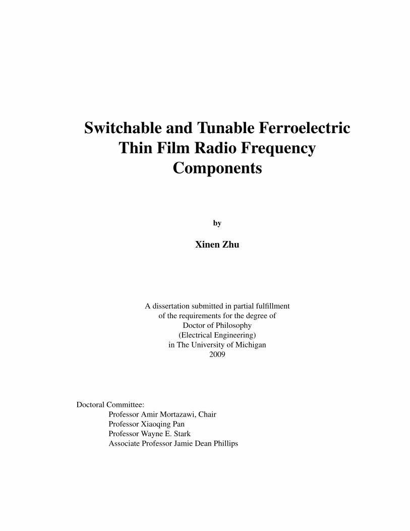
Switchable and Tunable FerroelectricThin Film Radio Frequency
Components
by
Xinen Zhu
A dissertation submitted in partial fulfillmentof the requirements for the degree of
Doctor of Philosophy(Electrical Engineering)
in The University of Michigan2009
Doctoral Committee:Professor Amir Mortazawi, ChairProfessor Xiaoqing PanProfessor Wayne E. StarkAssociate Professor Jamie Dean Phillips

© Xinen Zhu
All Rights Reserved
2009

to my wife Fang Ji (Gloria) and my parents
ii

Acknowledgments
I would like to express my deepest gratitude to my advisor, Prof. Amir Mortazawi, for his
constant support, guidance and encouragement during my graduate study at the University
of Michigan. From him, I learned how to be an independent researcher, as well as a great
deal of technical knowledge and skills. I would also like to thank Prof. Xiaoqing Pan, Prof.
Wayne E. Stark and Prof. Jamie D. Phillips for their advice and suggestion by being on my
dissertation committee.
I would like to especially thank Prof. Jamie D. Phillips to provide the pulsed laser
deposition system to this research. Without this system, this work will not even start. I
would like to thank Prof. Phillips and former and currents student in his group, including
Dr. Ding-Yuan Chen, Willie Bowen, Emine Cagin, Jeff Siddiqui and Weiming Wang, for
all the help and discussion on this deposition system.
I would like to thank former and current group members of Prof. Mortazawi, Dr. Ay-
man Al-Zayed, Dr. Jonghoon Choi, Dr. Xin Jiang, Dr. Lora Schulwitz, Dr. Ali Tombak,
Dr. Jin Zhang, Waleed Alomar, Seyit Ahmet Sis, Meng-Hung Chen, Danial Ehyaie, Jia-
Shiang (Josh) Fu, Victor Lee, Morteza Nick. Also I would like to thank all the students and
staff in the Radiation Lab.
This work will not be possible without the help and support from all the staff in the
Lurie Nanofabrication Lab. I would like to express my appreciation to Dr. Dennis Gri-
mard, Gregory Allion, Katharin Beach, Terre Briggs, Timothy Brock, Russ Clifford, Phil
Collica, Ning Gulari, Robert Hower, James Kulman, Sandrine Martin, Dennis Schweiger,
Edward Tang and Brian VanDerElzen.
I would like to thank all the brothers and sisters at Ann Arbor Chinese Christian Church
iii

and Jiayin Fellowship for their love and support. Especially I would to thank Pastor Teo,
Michael Man, Shou-Chin Man, Paul Chao, Alice Chao, Dongxuan Shen, Shiyan Chen for
their love, fellowship and spiritual guidance.
Finally I would like to sincerely thank my parents Xuekang Zhu and Peiqi Xu, my wife
Fang Ji and my daughter Priscilla Zhu for their constant love and support.
iv
Table of Contents
Dedication . . . . . . . . . . . . . . . . . . . . . . . . . . . . . . . . . . . . . . . ii
Acknowledgments . . . . . . . . . . . . . . . . . . . . . . . . . . . . . . . . . . . iii
List of Tables . . . . . . . . . . . . . . . . . . . . . . . . . . . . . . . . . . . . . . vii
List of Figures . . . . . . . . . . . . . . . . . . . . . . . . . . . . . . . . . . . . . viii
List of Appendices . . . . . . . . . . . . . . . . . . . . . . . . . . . . . . . . . . . xi
Chapter 1 INTRODUCTION . . . . . . . . . . . . . . . . . . . . . . . . . . . . 11.1 An Overview of Varactor Technologies . . . . . . . . . . . . . . . . . . . . 5
1.1.1 Semiconductor Varactor Diodes . . . . . . . . . . . . . . . . . . . 51.1.2 MEMS Varactors . . . . . . . . . . . . . . . . . . . . . . . . . . . 6
1.2 An Overview of Resonator Technologies . . . . . . . . . . . . . . . . . . . 71.2.1 Piezoelectric Materials Based Resonators . . . . . . . . . . . . . . 71.2.2 Polysilicon Vibrating Micromechanical Resonators . . . . . . . . . 10
1.3 Ferroelectric Thin Film Technology . . . . . . . . . . . . . . . . . . . . . 111.4 Thesis Overview and Outline . . . . . . . . . . . . . . . . . . . . . . . . . 15
Chapter 2 TWO PORT MEASUREMENT TECHNIQUE FOR CHARAC-TERIZING FERROELECTRIC THIN FILMS . . . . . . . . . . . . . . . . . 172.1 Introduction . . . . . . . . . . . . . . . . . . . . . . . . . . . . . . . . . . 172.2 Review of Measurement Techniques for Ferroelectric Thin Films . . . . . . 18
2.2.1 Coplanar Waveguide (CPW) Transmission Lines Method . . . . . . 192.2.2 Planar Printed Circuit Resonators Method . . . . . . . . . . . . . . 222.2.3 Capacitors Method . . . . . . . . . . . . . . . . . . . . . . . . . . 23
2.3 Modeling of Parallel Plate Capacitors . . . . . . . . . . . . . . . . . . . . 252.4 De-embedding Techniques of Parallel Plate Capacitors . . . . . . . . . . . 29
2.4.1 One Port Measurement Technique Using Signal-Ground (SG)Probes . . . . . . . . . . . . . . . . . . . . . . . . . . . . . . . . 29
2.4.2 One Port Measurement Technique Using GSG Probes . . . . . . . 312.4.3 Two Port Measurement Technique Using GSG Probes . . . . . . . 32
2.5 Uncertainty Study . . . . . . . . . . . . . . . . . . . . . . . . . . . . . . . 342.6 Measurement Results . . . . . . . . . . . . . . . . . . . . . . . . . . . . . 402.7 Conclusion . . . . . . . . . . . . . . . . . . . . . . . . . . . . . . . . . . 41
v
Chapter 3 FABRICATION OF FERROELECTRIC THIN FILM VARAC-TORS AND THEIR APPLICATION IN MICROWAVE TUNABLE CIR-CUITS . . . . . . . . . . . . . . . . . . . . . . . . . . . . . . . . . . . . . . . 433.1 Optimization of Ferroelectric Thin Films Deposited by Pulsed Laser De-
position . . . . . . . . . . . . . . . . . . . . . . . . . . . . . . . . . . . . 433.1.1 Pulsed Laser Deposition Process . . . . . . . . . . . . . . . . . . . 443.1.2 Deposition Parameter Optimization . . . . . . . . . . . . . . . . . 45
3.2 Clean Room Fabrication Process . . . . . . . . . . . . . . . . . . . . . . . 513.3 Microwave Tunable Circuit Applications . . . . . . . . . . . . . . . . . . . 543.4 Conclusion . . . . . . . . . . . . . . . . . . . . . . . . . . . . . . . . . . 56
Chapter 4 TUNABLE MICROWAVE FILTER USING BST VARACTORS . . 574.1 Introduction . . . . . . . . . . . . . . . . . . . . . . . . . . . . . . . . . . 574.2 Capacitively Loaded Ring Resonators . . . . . . . . . . . . . . . . . . . . 584.3 A Three Pole Bandpass Filter Design . . . . . . . . . . . . . . . . . . . . . 604.4 Filter Fabrication . . . . . . . . . . . . . . . . . . . . . . . . . . . . . . . 614.5 Filter Measurement Results . . . . . . . . . . . . . . . . . . . . . . . . . . 624.6 Conclusion . . . . . . . . . . . . . . . . . . . . . . . . . . . . . . . . . . 63
Chapter 5 SWITCHABLE ACOUSTIC WAVE RESONATORS AND FIL-TERS USING FERROELECTRIC THIN FILMS . . . . . . . . . . . . . . . 665.1 Introduction . . . . . . . . . . . . . . . . . . . . . . . . . . . . . . . . . . 665.2 Piezoelectricity and Electrostriction . . . . . . . . . . . . . . . . . . . . . 675.3 Thickness Mode Acoustic Wave Resonators Design . . . . . . . . . . . . . 695.4 Contour Mode Acoustic Wave Ring Resonator Design . . . . . . . . . . . 715.5 Ladder Type FBAR Filters Design . . . . . . . . . . . . . . . . . . . . . . 735.6 Fabrication Process and Measurement Results . . . . . . . . . . . . . . . . 76
5.6.1 BST FBARs . . . . . . . . . . . . . . . . . . . . . . . . . . . . . 765.6.2 A 1.5 Stage Ladder Type BTO FBAR Filter . . . . . . . . . . . . . 795.6.3 Contour Mode Acoustic Wave Resonators . . . . . . . . . . . . . . 85
5.7 Conclusion . . . . . . . . . . . . . . . . . . . . . . . . . . . . . . . . . . 89
Chapter 6 CONCLUSIONS AND FUTURE WORK . . . . . . . . . . . . . . . 906.1 Conclusions . . . . . . . . . . . . . . . . . . . . . . . . . . . . . . . . . . 906.2 Future Work . . . . . . . . . . . . . . . . . . . . . . . . . . . . . . . . . . 91
6.2.1 Low Temperature Deposition of Ferroelectric Thin Films UsingAtomic Layer Deposition . . . . . . . . . . . . . . . . . . . . . . . 91
6.2.2 Higher Frequency Switchable Contour Mode Resonators UsingFerroelectric Thin Films . . . . . . . . . . . . . . . . . . . . . . . 92
6.2.3 High Performance Switchable FBAR Filters Using FerroelectricThin Films . . . . . . . . . . . . . . . . . . . . . . . . . . . . . . 93
Appendices . . . . . . . . . . . . . . . . . . . . . . . . . . . . . . . . . . . . . . . 94
Bibliography . . . . . . . . . . . . . . . . . . . . . . . . . . . . . . . . . . . . . . 110
vi

List of Tables
Table1.1 Comparison of varactor technologies [1] . . . . . . . . . . . . . . . . . . . 135.1 Acoustic and physical parameters of the layers in BST FBAR . . . . . . . . 715.2 Material properties of BTO thin films . . . . . . . . . . . . . . . . . . . . 735.3 Modified Butterworth-Van Dyke circuit model for the fabricated BST FBAR 78
vii
List of Figures
Figure1.1 Internal circuit board of an iPhone 3G, taken from www.eetimes.com. . . . 21.2 Tunable front-end block diagram . . . . . . . . . . . . . . . . . . . . . . . 31.3 A commercial 8-band switchable filter bank from Akon Inc. . . . . . . . . 41.4 MEMS varactors . . . . . . . . . . . . . . . . . . . . . . . . . . . . . . . 61.5 Surface acoustic wave devices . . . . . . . . . . . . . . . . . . . . . . . . 81.6 FBAR with (a) air cavity and (b) Bragg reflector . . . . . . . . . . . . . . . 91.7 Contour mode vibrating micromechanical resonator [2] . . . . . . . . . . . 101.8 Polarization versus electric field for (a) normal dielectrics, (b) ferroelectrics
when T > Tc and (c) ferroelectrics with T < Tc. . . . . . . . . . . . . . . . 121.9 (a) The cell structure and (b) the typical CV curve of BST . . . . . . . . . . 121.10 Switchable ferroelectric FBAR filter bank in reconfigurable front-end
transceivers . . . . . . . . . . . . . . . . . . . . . . . . . . . . . . . . . . 142.1 CPW line on ferroelectric thin film . . . . . . . . . . . . . . . . . . . . . . 192.2 CPW resonator on ferroelectric thin film . . . . . . . . . . . . . . . . . . . 222.3 Conventional capacitors and the model . . . . . . . . . . . . . . . . . . . . 242.4 RF current density on a) the parallel plate capacitor and b) the electrode only 262.5 Circuit model of parallel plate capacitors . . . . . . . . . . . . . . . . . . . 272.6 Simplified circuit model of parallel plate capacitors . . . . . . . . . . . . . 272.7 Physical layouts and circuit models for one port measurement using SG probe 302.8 Physical layout and circuit model for one port measurement using GSG
probes . . . . . . . . . . . . . . . . . . . . . . . . . . . . . . . . . . . . . 322.9 Physical layout and circuit model for two port measurement using GSG
probes . . . . . . . . . . . . . . . . . . . . . . . . . . . . . . . . . . . . . 332.10 Comparison of the uncertainty of S11 magnitude and phase under different
IF BW and average factors . . . . . . . . . . . . . . . . . . . . . . . . . . 362.11 Comparison of the uncertainty of S21 magnitude and phase under different
IF BW and average factors . . . . . . . . . . . . . . . . . . . . . . . . . . 372.12 Comparison of the uncertainty in the loss tangent for BST thin films with
different loss tangent values using one port measurement technique. . . . . 392.13 Comparison of uncertainty of loss tangent using one port and two port mea-
surement techniques . . . . . . . . . . . . . . . . . . . . . . . . . . . . . . 392.14 Comparison of uncertainty of capacitance using one port and two port mea-
surement techniques . . . . . . . . . . . . . . . . . . . . . . . . . . . . . . 40
viii
2.15 Comparison of loss tangent with/without de-embeding using two port mea-surement technique . . . . . . . . . . . . . . . . . . . . . . . . . . . . . . 41
2.16 Extracted loss tangent of the BST thin film . . . . . . . . . . . . . . . . . . 422.17 Extracted relative permittivity of the BST thin film . . . . . . . . . . . . . 423.1 Illustration of a typical PLD setup. . . . . . . . . . . . . . . . . . . . . . . 453.2 C-V tuning curves for BST thin films deposited at 500, 600 and 700 degrees 463.3 Illustration of the oxygen vacancies in the BST thin films . . . . . . . . . . 473.4 Loss tangent of the BST thin films under different partial oxygen pressure
and annealing conditions . . . . . . . . . . . . . . . . . . . . . . . . . . . 483.5 Loss tangent of the BST thin films under two different laser fluence . . . . 493.6 C-V tuning curves of the BST thin film (a) without and (b) with the post
process oxygen annealing . . . . . . . . . . . . . . . . . . . . . . . . . . . 503.7 Device Q factor of the BST varactor with optimized PLD deposition con-
ditions . . . . . . . . . . . . . . . . . . . . . . . . . . . . . . . . . . . . . 523.8 XRD measurement of BST thin films with optimized PLD deposition con-
ditions . . . . . . . . . . . . . . . . . . . . . . . . . . . . . . . . . . . . . 523.9 Process flow of ferroelectric thin film based varactors and circuits . . . . . 533.10 Single and 5x5 stacked BST varactor . . . . . . . . . . . . . . . . . . . . . 543.11 BST varactor tuned phase shifter . . . . . . . . . . . . . . . . . . . . . . . 553.12 BST varactor based impedance tuner . . . . . . . . . . . . . . . . . . . . . 554.1 (a) Half wavelength, (b) quarter wavelength, (c) capacitvely loaded quarter
wavelength and (d) capacitively loaded ring resonator . . . . . . . . . . . . 584.2 Input impedance magnitude of (a) half wavelength, (b) quarter wavelength,
(c) capacitively loaded quater wavelength and (d) capacitively loaded ringresonator . . . . . . . . . . . . . . . . . . . . . . . . . . . . . . . . . . . 59
4.3 Layout of 3 pole tunable filter . . . . . . . . . . . . . . . . . . . . . . . . 604.4 Micro-graph of fabricated 3 pole tunable filter . . . . . . . . . . . . . . . . 624.5 Measured filter response when no DC bias is applied. . . . . . . . . . . . . 634.6 (a)Insertion loss and (b) return loss of the tunable microwave filter with DC
bias voltage from 0 V to 10 V. . . . . . . . . . . . . . . . . . . . . . . . . 645.1 BST FBAR structure . . . . . . . . . . . . . . . . . . . . . . . . . . . . . 695.2 BST FBAR simulation comparison with/without the silicon substrate . . . . 715.3 Thickness mode and contour mode acoustic wave resonators. . . . . . . . . 725.4 Contour mode ring resonator . . . . . . . . . . . . . . . . . . . . . . . . . 735.5 The relationship between resonance frequency and the lateral dimension of
circular ring BTO thin film contour mode resonators. . . . . . . . . . . . . 745.6 Ladder type FBAR filter . . . . . . . . . . . . . . . . . . . . . . . . . . . 745.7 One L-section in ladder type FBAR filters . . . . . . . . . . . . . . . . . . 755.8 Out-of-band rejection versus capacitance ratio and the number of L-
sections cascaded. . . . . . . . . . . . . . . . . . . . . . . . . . . . . . . . 765.9 Cross view and photograph of the fabricated BST FBAR . . . . . . . . . . 775.10 Reflection coefficient of the BST FBAR when DC bias is (a) ON and (b) OFF 785.11 Magnitude of the input impedance of the BST FBAR . . . . . . . . . . . . 79
ix
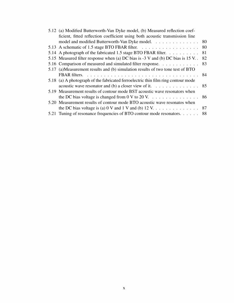
5.12 (a) Modified Butterworth-Van Dyke model, (b) Measured reflection coef-ficient, fitted reflection coefficient using both acoustic transmission linemodel and modified Butterworth-Van Dyke model. . . . . . . . . . . . . . 80
5.13 A schematic of 1.5 stage BTO FBAR filter. . . . . . . . . . . . . . . . . . 805.14 A photograph of the fabricated 1.5 stage BTO FBAR filter. . . . . . . . . . 815.15 Measured filter response when (a) DC bias is -3 V and (b) DC bias is 15 V. . 825.16 Comparison of measured and simulated filter response. . . . . . . . . . . . 835.17 (a)Measurement results and (b) simulation results of two tone test of BTO
FBAR filters. . . . . . . . . . . . . . . . . . . . . . . . . . . . . . . . . . 845.18 (a) A photograph of the fabricated ferroelectric thin film ring contour mode
acoustic wave resonator and (b) a closer view of it. . . . . . . . . . . . . . 855.19 Measurement results of contour mode BST acoustic wave resonators when
the DC bias voltage is changed from 0 V to 20 V. . . . . . . . . . . . . . . 865.20 Measurement results of contour mode BTO acoustic wave resonatos when
the DC bias voltage is (a) 0 V and 1 V and (b) 12 V. . . . . . . . . . . . . . 875.21 Tuning of resonance frequencies of BTO contour mode resonators. . . . . . 88
x

List of Appendices
AppendixA Ferroelectric Thin Film Based Tunable Capacitors and Circuits Fabrication
Process . . . . . . . . . . . . . . . . . . . . . . . . . . . . . . . . . . . . . 95A.1 Starting wafer: Sapphire, single-side polished, C-plane, 430 µm. . . . . . . 95A.2 Bottom electrode evaporation and liftoff. . . . . . . . . . . . . . . . . . . . 95A.3 Ferroelectric thin film deposition by PLD. . . . . . . . . . . . . . . . . . . 96A.4 Top electrode evaporation and liftoff. . . . . . . . . . . . . . . . . . . . . . 96A.5 High temperature oxygen annealing. . . . . . . . . . . . . . . . . . . . . . 97A.6 Ferroelectric thin film wet etch. . . . . . . . . . . . . . . . . . . . . . . . . 97A.7 Bias networks sputter and liftoff. . . . . . . . . . . . . . . . . . . . . . . . 98A.8 Contact metal evaporation and liftoff. . . . . . . . . . . . . . . . . . . . . 98A.9 Passivation layer deposition by PECVD. . . . . . . . . . . . . . . . . . . . 99A.10 Passivation layer wet etch. . . . . . . . . . . . . . . . . . . . . . . . . . . 99A.11 Circuit metal evaporation and liftoff. . . . . . . . . . . . . . . . . . . . . . 100A.12 Gold electro-plating. . . . . . . . . . . . . . . . . . . . . . . . . . . . . . 101A.13 Metal etch back. . . . . . . . . . . . . . . . . . . . . . . . . . . . . . . . . 101B Ferroelectric Thin Film Based Switchable Acoustic Wave Resonators and
Filters Fabrication Process . . . . . . . . . . . . . . . . . . . . . . . . . . . 103B.1 Starting wafer: high resistivity Silicon, 525 µm, with 1 µm thermal silicon
dioxide. . . . . . . . . . . . . . . . . . . . . . . . . . . . . . . . . . . . . 103B.2 Bottom electrode evaporation and liftoff. . . . . . . . . . . . . . . . . . . . 103B.3 SiO2 wet etch. . . . . . . . . . . . . . . . . . . . . . . . . . . . . . . . . . 104B.4 Ferroelectric thin film deposition by PLD. . . . . . . . . . . . . . . . . . . 105B.5 Top electrode evaporation and liftoff. . . . . . . . . . . . . . . . . . . . . . 105B.6 High temperature oxygen annealing. . . . . . . . . . . . . . . . . . . . . . 106B.7 Ferroelectric thin film wet etch. . . . . . . . . . . . . . . . . . . . . . . . . 106B.8 Bias networks sputter and liftoff. . . . . . . . . . . . . . . . . . . . . . . . 107B.9 Contact metal evaporation and liftoff. . . . . . . . . . . . . . . . . . . . . 107B.10 Silicon Micromechining Process . . . . . . . . . . . . . . . . . . . . . . . 108
B.10.1 First generation: back side deep reactive ion etching (DRIE) usingSTS . . . . . . . . . . . . . . . . . . . . . . . . . . . . . . . . . . 108
B.10.2 Second generation: top side etching using XeF2 . . . . . . . . . . . 109
xi
Chapter 1
INTRODUCTION
Today’s wireless communication systems advance steadily with improved system perfor-
mance, increased functionality, reduced size and cost. For example, mobile phone stan-
dards have been evolved from the second generation (2G) with low date rate voice service
to the third generation (3G) with higher date rate services such as video calls and wireless
broadband data access. As one of the 3G technologies, UMTS 1 operates in the frequency
bands of 850/900/1700/1900/2100 MHz over the globe. For seamless connection to the
3G network, mobile phones are required to operate over all these frequency bands. Other
than the cellular service, there are new functional services such as the GPS 2 in the 1.5
GHz band, and the Wi-Fi in the 2.4/5.0 GHz bands. Therefore, it is highly desirable for
the end users to have a multi-band and multi-mode wireless handheld device. At the same
time it is quite a challenge for microwave engineers to have an elegant and cost effective
transceiver design for multi-band and multi-mode operations. The conventional approach
to design a multi-band multi-mode radio frequency transceiver is to switch among a number
of sub-transceivers for each frequency band or mode. This approach is a straightforward
implementation, however it results in increased complexity, larger size, and higher cost.
An example using the conventional multi-band transceiver design is the iPhone 3G [3].
It is a tri-band 3G smart phone, and commercially available nowadays. In the transmitter
side, it has three TriQuint power amplifier (PA) modules for UMTS 850/1900/2100 MHz
bands and a quad-band PA module from Skyworks for the GSM 3 850/900/1800/1900 MHz
1Universal Mobile Telecommunications System2Global Positioning System3Global Systems for Mobile communications
1
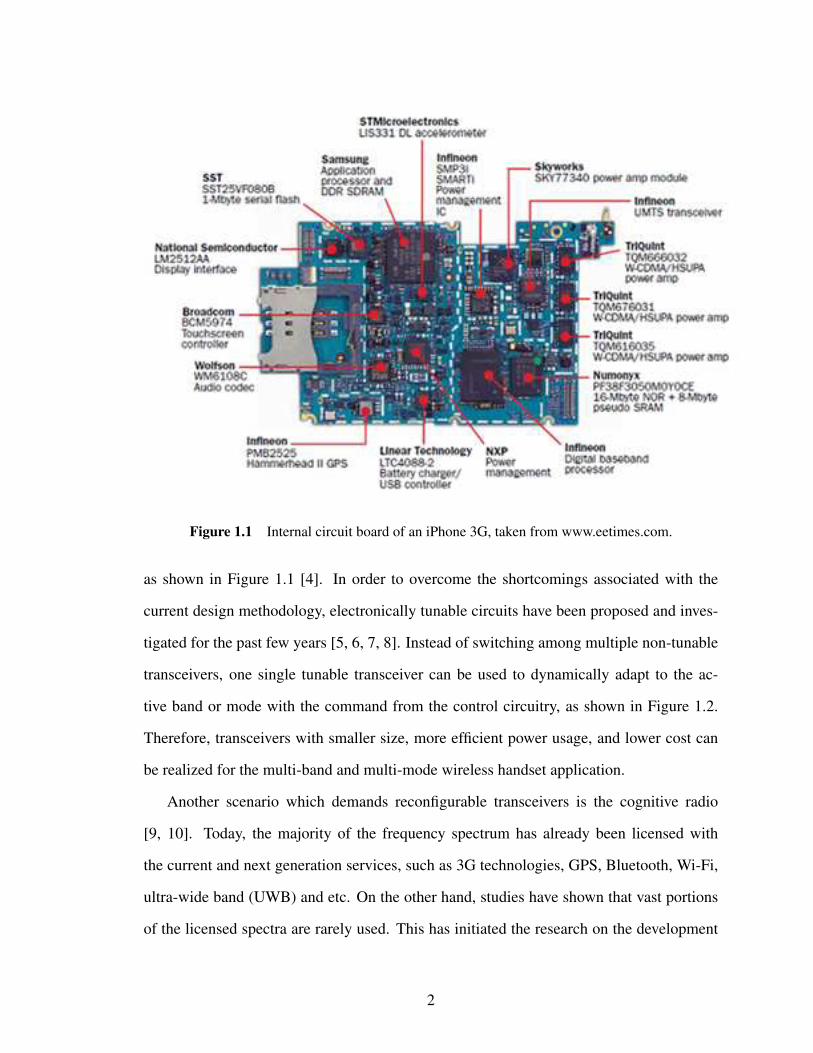
Figure 1.1 Internal circuit board of an iPhone 3G, taken from www.eetimes.com.
as shown in Figure 1.1 [4]. In order to overcome the shortcomings associated with the
current design methodology, electronically tunable circuits have been proposed and inves-
tigated for the past few years [5, 6, 7, 8]. Instead of switching among multiple non-tunable
transceivers, one single tunable transceiver can be used to dynamically adapt to the ac-
tive band or mode with the command from the control circuitry, as shown in Figure 1.2.
Therefore, transceivers with smaller size, more efficient power usage, and lower cost can
be realized for the multi-band and multi-mode wireless handset application.
Another scenario which demands reconfigurable transceivers is the cognitive radio
[9, 10]. Today, the majority of the frequency spectrum has already been licensed with
the current and next generation services, such as 3G technologies, GPS, Bluetooth, Wi-Fi,
ultra-wide band (UWB) and etc. On the other hand, studies have shown that vast portions
of the licensed spectra are rarely used. This has initiated the research on the development
2

Figure 1.2 Tunable front-end block diagram
of cognitive radios, where secondary (i.e., unlicensed) users are allowed to transmit and
receive data over portions of spectra when primary (i.e., licensed) users are inactive. In
other words, the radio is able to change its transmission or reception parameters such as
operation frequency and power level to communicate efficiently avoiding interference with
licensed or unlicensed users. This alteration of parameters is based on the active monitoring
of several factors in the external and internal radio environment, such as radio frequency
spectrum, user behavior and network state. One of key circuits in cognitive radios is a
switchable filter bank. It is a band or channel selection system over a wide frequency range
through switching among a number of sub-band or channel bandpass filters. In the tradi-
tional design of switchable filter banks, there are input and output switches, a number of
bandpass filters, and the bias matrix associated with the switches. An example of conven-
tional switchable filter bank [11] is shown in Figure 1.3. Switchable filter banks based on
current filter technologies require external switches using solid state or MEMS devices.
Incorporating external switches in the path of RF signal results in increased loss, circuit
complexity and cost. Instead, intrinscically switchable resonators can be used to design
switchable filter banks with less loss, smaller footprint and less cost.
3

Figure 1.3 A commercial 8-band switchable filter bank from Akon Inc.
The key components for the aforementioned reconfigurable RF and microwave transceivers
are reconfigurable devices such as tunable capacitors (varactors) and intrinsically switch-
able resonators. The change of the capacitance in varactors can be achieved by mechanical
tuning [12], magnetical tuning [13] and electronically tuning [14, 15, 16]. Electronically
tunable capacitors are preferred due to their small size, light weight and monolithic inte-
gration with active devices. Various electronically reconfigurable circuits can be designed,
such as tunable antennas (change of the frequency, polarization, radiation pattern, or any
combination of them), tunable bandpass filters, adaptive matching networks for PAs, phase
shifters, tunable amplifiers, and voltage controlled oscillators. Depending on the function-
ality of each circuit, the performance gain by using varactors will be improved operation
frequency range, efficient power usage, reduced size or less cost. Intrinsically switchable
resonators are the resonators that can be turned on and off by the application of the DC
bias. The switching process is achieved by the intrinsic property of resonators other than
the external switches. For switchable resonators with a miniaturized size and a high Q fac-
tor, one can envision to integrate a number of such resonators monolithically for wide-band
frequency generation and selection in a compact size with no external switches involved.
4
Both varactors and switchable resonators can be characterized with the similar performance
measures which are summarized below:
• Tunability for varactors (Cmax/Cmin), and frequency tuning for switchable res-
onators.
• Quality factor.
• Control voltage.
• Power handling capability.
• Linearity.
• Tuning or switching speed.
This work proposes ferroelectric thin films as a viable solution to both high perfor-
mance RF and microwave varactors and intrinsically switchable resonators. In the next two
sections, various varactor and resonator technologies which are currently employed in the
wireless communication systems will be discussed to understand their inadequacy for the
future challenges and the need of a replacement by the proposed ferroelectric thin films
technology.
1.1 An Overview of Varactor Technologies
Microwave varactors are important to the design of tunable microwave circuits. Two varac-
tor technologies are described in this section. They are semiconductor varactor diodes and
microelectromechanical system (MEMS) varactors.
1.1.1 Semiconductor Varactor Diodes
A semiconductor varactor diode is a p-n junction diode made of Gallium-Arsenide (GaAs),
Silicon (Si) or Silicon-Germanium (SiGe). The depletion area in the p-n junction forms
a capacitor, whose capacitance can be varied by changing the reverse bias voltage across
the diode. As a mature varactor technology, varactor diodes are commercially available at
5

Figure 1.4 MEMS varactors
very low cost. The advantages of varactor diodes include large tenability (> 10 : 1), small
footprint, fast tuning speed and low control voltage. However, their disadvantage is the
poor Q-factor which decreases as the operating frequency increases. Tunable circuits using
varactor diodes exhibit considerable amount of loss beyond 5 GHz. Another drawback of
semiconductor varactors is their poor power handling capability because the reverse bias
requirement doesn’t allow for large RF voltage swing across the diode.
1.1.2 MEMS Varactors
Radio frequency (RF) MEMS have been actively researched over the last decade in both
industry and academia. They are 3D mechanical structures built on the low cost substrates
(alumina, quartz, Si) using mature semiconductor processing and surface micro-machining
techniques. Two major RF MEMS devices are switches [17, 18] and varactors [15]. The
basic structure consists of two metal traces (signal and ground) separated vertically by an
air gap, which forms a parallel-plate capacitor, as shown in Figure 1.4. When a DC bias
voltage is applied between the upper bridge and the lower signal trace, the resultant elec-
trostatic force pulls down the thin bridge arm. Therefore the capacitance increases. Further
6

increase of the DC bias voltage causes collapse of the bridge arm to the signal trace, there-
fore short circuiting the device. Due to the mechanical rigidness, the change of the bridge
gap is limited to one third of its original value. Therefore MEMS varactors suffer from low
tunabilities of approximately 1.5:1 with typical tuning voltage requirements in the range of
50-100 V. While MEMS varactors are superior in the Q factor and linearity, they do face
practical challenges of reliability and expensive hermetic packaging.
1.2 An Overview of Resonator Technologies
1.2.1 Piezoelectric Materials Based Resonators
Piezoelectricity was first discovered in 1880 by the Curie brothers. The word piezo is de-
rived from Greek piezein, which means to squeeze or stress. As revealed in the name, the
piezoelectric effect describes the ability to induce an electrical polarization by the applied
mechanical stress in crystals of certain classes. It is also called direct piezoelectric effect.
The converse piezoelectric effect is defined as the production of a mechanical stress by the
applied electric field. Piezoelectricity is a reversible phenomenon that expresses a linear in-
teraction between mechanical and electrical domains in a single elastic body. This relation
is mathematically defined as below.
S = sET +dT E (1.1)
D = dT + εT E (1.2)
where S is strain, s is compliance, T is stress, D is electric displacement, d is piezoelec-
tric coefficient, ε is permittivity, E is electric field strength; superscript E indicates a zero
or constant electric field, and superscript T a zero or constant stress field.
Crystals can be classified into 32 point groups according to their crystallographic sym-
7
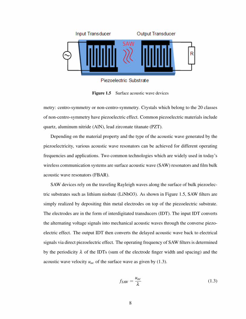
Figure 1.5 Surface acoustic wave devices
metry: centro-symmetry or non-centro-symmetry. Crystals which belong to the 20 classes
of non-centro-symmetry have piezoelectric effect. Common piezoelectric materials include
quartz, aluminum nitride (AlN), lead zirconate titanate (PZT).
Depending on the material property and the type of the acoustic wave generated by the
piezoelectricity, various acoustic wave resonators can be achieved for different operating
frequencies and applications. Two common technologies which are widely used in today’s
wireless communication systems are surface acoustic wave (SAW) resonators and film bulk
acoustic wave resonators (FBAR).
SAW devices rely on the traveling Rayleigh waves along the surface of bulk piezoelec-
tric substrates such as lithium niobate (LiNbO3). As shown in Figure 1.5, SAW filters are
simply realized by depositing thin metal electrodes on top of the piezoelectric substrate.
The electrodes are in the form of interdigitated transducers (IDT). The input IDT converts
the alternating voltage signals into mechanical acoustic waves through the converse piezo-
electric effect. The output IDT then converts the delayed acoustic wave back to electrical
signals via direct piezoelectric effect. The operating frequency of SAW filters is determined
by the periodicity λ of the IDTs (sum of the electrode finger width and spacing) and the
acoustic wave velocity uac of the surface wave as given by (1.3).
fSAW =uac
λ(1.3)
8
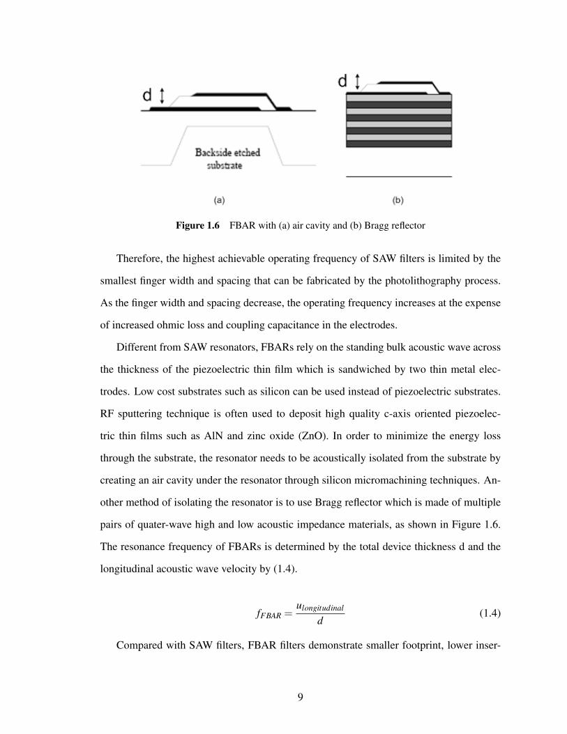
Figure 1.6 FBAR with (a) air cavity and (b) Bragg reflector
Therefore, the highest achievable operating frequency of SAW filters is limited by the
smallest finger width and spacing that can be fabricated by the photolithography process.
As the finger width and spacing decrease, the operating frequency increases at the expense
of increased ohmic loss and coupling capacitance in the electrodes.
Different from SAW resonators, FBARs rely on the standing bulk acoustic wave across
the thickness of the piezoelectric thin film which is sandwiched by two thin metal elec-
trodes. Low cost substrates such as silicon can be used instead of piezoelectric substrates.
RF sputtering technique is often used to deposit high quality c-axis oriented piezoelec-
tric thin films such as AlN and zinc oxide (ZnO). In order to minimize the energy loss
through the substrate, the resonator needs to be acoustically isolated from the substrate by
creating an air cavity under the resonator through silicon micromachining techniques. An-
other method of isolating the resonator is to use Bragg reflector which is made of multiple
pairs of quater-wave high and low acoustic impedance materials, as shown in Figure 1.6.
The resonance frequency of FBARs is determined by the total device thickness d and the
longitudinal acoustic wave velocity by (1.4).
fFBAR =ulongitudinal
d(1.4)
Compared with SAW filters, FBAR filters demonstrate smaller footprint, lower inser-
9

Figure 1.7 Contour mode vibrating micromechanical resonator [2]
tion loss, sharper roll-off, higher power handling capability and IC compatibility. FBAR
duplexers are commercially available for PCS and WCDMA.
1.2.2 Polysilicon Vibrating Micromechanical Resonators
With the advances in MEMS fabrication technology, 3D objects with a wide variety of
geometries can be easily realized in micro scale size. This has helped to accelerate the re-
search in vibrating micromechanical resonators over the past decade. Given the resonator
structure and its material properties, the resonance mode shape and its corresponding fre-
quency can be determined. Clamp-clamp beam resonators have been demonstrated at 10
MHz with a Q-factor of 8000 in vacuum [19]. Wine-glass dish resonators can operate at 62
MHz with a Q-factor of 161,000 [20]. Contour mode dish resonators were demonstrated
at 1.5 GHz with a Q-factor of 11,555 [2]. The operation of the vibrating micromechan-
ical resonators is based on the mechanical vibration of the resonator body excited by an
external force, which is achieved by electrostatic capacitive transduction. A contour mode
10

dish resonator in the two port configuration is shown in Figure 1.7. The input and output
capacitive transducer electrodes are separated from the dish body by a 100 nm air gap. By
applying DC bias Vp to the dish and the small signal vi to the input electrode, the resonator
can be excited. The electrostatic force is expressed in (1.5).
Fi =12(∂C1
∂ r)(Vp− vi)2 =−Vp(
∂C1
∂ r)vi (1.5)
As the frequency of vi matches the natural resonance frequency of the contour mode
disk, the disk vibrates in the fashion of radial extraction and contraction around its perime-
ter by the electrostatic force Fi. Furthemore, the resonator can be turned on or off by the
application of the DC bias Vp.
Vibrating micromechanical resonators have many attractive advantages such as, small
size, easy integration with silicon IC process, self-switching capability, high Q-factors and
single wafer multi-frequency resonators integration. However, these resonators have a very
large motional resistance (over tens of kΩ) at the resonance frequency due to the large stiff-
ness of Polysilicon. This creates a significant impedance mismatch to the commonly used
50 Ω system impedance. Filters based on this technology present impractical insertion loss
even though the resonator itself is almost lossless [21].
1.3 Ferroelectric Thin Film Technology
Ferroelectric materials are a class of dipolar dielectric materials that exhibit a spontaneous
electrical polarization which can be reversed by the application of an external electric field.
This unique characteristic has been a very interesting research topic in both fundamental
physics as well as in various mechanical, electrical engineering since ferroelectricity was
first discovered in 1920.
In normal dielectric materials, the electrical polarization is linearly dependent on the
applied electric field, shown in Figure 1.8 (a). Therefore, the resultant permittivity, which
11

Figure 1.8 Polarization versus electric field for (a) normal dielectrics, (b) ferroelectrics whenT > Tc and (c) ferroelectrics with T < Tc.
Figure 1.9 (a) The cell structure and (b) the typical CV curve of BST
is equal to the slope of the polarization versus E-field (PE) curve, is a fixed quantity. Fer-
roelectric materials have a characteristic structural phase transition temperature called the
Curie temperature, Tc. Below Tc, ferroelectric materials demonstrate a non-zero sponta-
neous polarization when no E-field is applied. The spontaneous polarization in ferroelectric
materials can be reversed by the application of an external E-field, which results in hystere-
sis loop, shown in Figure 1.8 (c). Above Tc, the material becomes paraelectric without a
spontaneous polarization. At the paraelectric phase, the polarization is a nonlinear function
of the applied E-field, as shown in Figure 1.8 (b), resulting in a nonlinear electric field
dependent permittivity. This enables one to fabricate electronically tunable capacitors for
reconfigurable RF/microwave transceiver application.
12
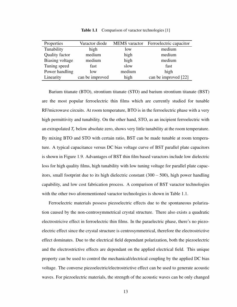
Table 1.1 Comparison of varactor technologies [1]
Properties Varactor diode MEMS varactor Ferroelectric capacitorTunability high low mediumQuality factor medium high mediumBiasing voltage medium high mediumTuning speed fast slow fastPower handling low medium highLinearity can be improved high can be improved [22]
Barium titanate (BTO), strontium titanate (STO) and barium strontium titanate (BST)
are the most popular ferroelectric thin films which are currently studied for tunable
RF/microwave circuits. At room temperature, BTO is in the ferroelectric phase with a very
high permittivity and tunability. On the other hand, STO, as an incipient ferroelectric with
an extrapolated Tc below absolute zero, shows very little tunability at the room temperature.
By mixing BTO and STO with certain ratio, BST can be made tunable at room tempera-
ture. A typical capacitance versus DC bias voltage curve of BST parallel plate capacitors
is shown in Figure 1.9. Advantages of BST thin film based varactors include low dielectric
loss for high quality films, high tunability with low tuning voltage for parallel plate capac-
itors, small footprint due to its high dielectric constant (300− 500), high power handling
capability, and low cost fabrication process. A comparison of BST varactor technologies
with the other two aforementioned varactor technologies is shown in Table 1.1.
Ferroelectric materials possess piezoelectric effects due to the spontaneous polariza-
tion caused by the non-centrosymmetrical crystal structure. There also exists a quadratic
electrostricive effect in ferroelectric thin films. In the paraelectric phase, there’s no piezo-
electric effect since the crystal structure is centrosymmetrical, therefore the electrostrictive
effect dominates. Due to the electrical field dependant polarization, both the piezoelectric
and the electrostrictive effects are dependant on the applied electrical field. This unique
property can be used to control the mechanical/electrical coupling by the applied DC bias
voltage. The converse piezoelectric/electrostrictive effect can be used to generate acoustic
waves. For piezoelectric materials, the strength of the acoustic waves can be only changed
13
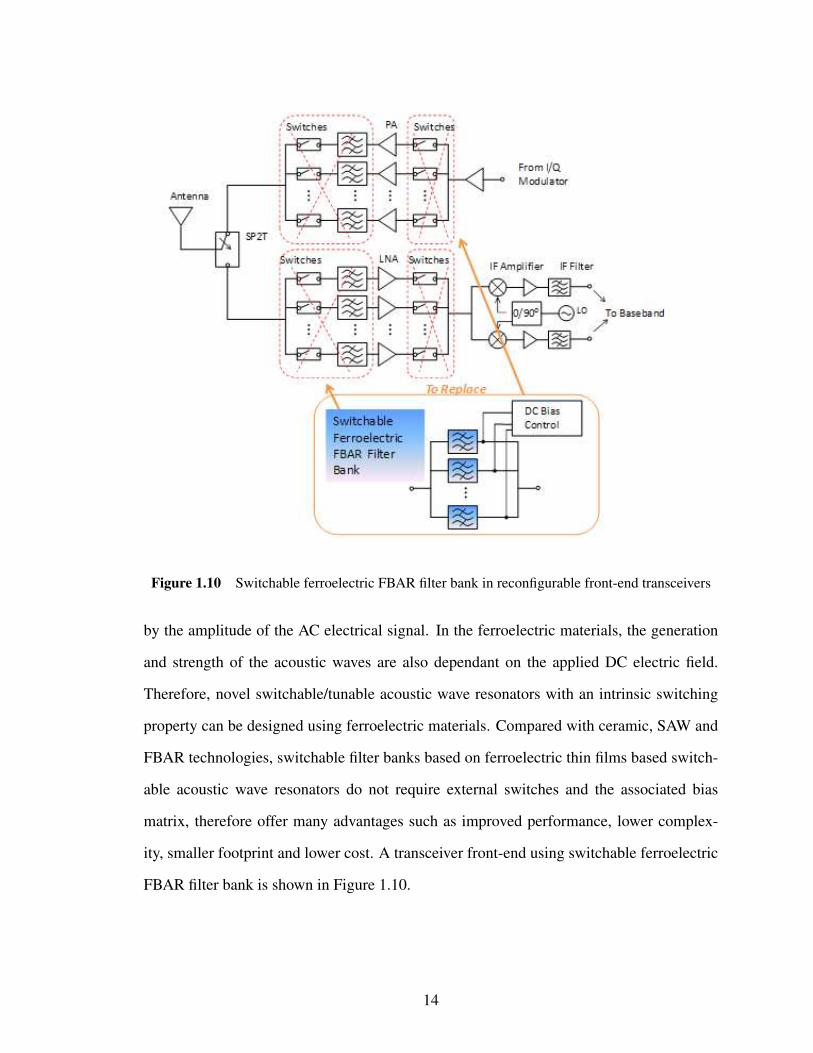
Figure 1.10 Switchable ferroelectric FBAR filter bank in reconfigurable front-end transceivers
by the amplitude of the AC electrical signal. In the ferroelectric materials, the generation
and strength of the acoustic waves are also dependant on the applied DC electric field.
Therefore, novel switchable/tunable acoustic wave resonators with an intrinsic switching
property can be designed using ferroelectric materials. Compared with ceramic, SAW and
FBAR technologies, switchable filter banks based on ferroelectric thin films based switch-
able acoustic wave resonators do not require external switches and the associated bias
matrix, therefore offer many advantages such as improved performance, lower complex-
ity, smaller footprint and lower cost. A transceiver front-end using switchable ferroelectric
FBAR filter bank is shown in Figure 1.10.
14

1.4 Thesis Overview and Outline
This thesis proposes to use ferroelectric thin films for both low cost high performance var-
actors and novel switchable acoustic wave resonators at RF and microwave frequencies.
This thesis covers a measurement technique for the characterization of ferroelectric thin
films at microwave frequencies, a clean room fabrication process and thin film deposition
optimization, BST varactors and tunable microwave circuits, novel switchable thickness
and lateral mode ferroelectric acoustic wave resonators and filters.
The organization of the thesis is as follows.
Chapter 2 discusses measurement and parameter extraction technique for the character-
ization of ferroelectric thin films. A two port measurement technique has been proposed in
order to determine the loss tangent and permittivity of the BST thin film easily and accu-
rately. Uncertainty studies show that the proposed two port measurement technique is more
accurate than the commonly used one port reflection technique by approximately 30%.
Chapter 3 discusses the fabrication process for BST varactors and tunable circuits. BST
thin films studied here are deposited by pulsed laser deposition technique. The influence
of the deposition conditions on the BST thin film has been studied. By optimizing the
substrate temperature, partial oxygen pressure, laser fluence and post process oxygen an-
nealing, BST thin films with a low loss tangent can be achieved. Several fabricated tunable
capacitors and circuits are presented.
Chapter 4 presents a tunable microwave filter using BST varactors. Capacitively loaded
ring resonators are used since their frequency can be easily tuned and they provide better
roll-off. A fully integrated 3 pole filter with a good tunability and moderate insertion loss
has been demonstrated.
Chapter 5 discusses the electrostrictive effect in the BST and BTO thin films and its
application for novel switchable acoustic wave resonators and filters. Thickness mode res-
onators are analyzed and simulated. The first working thickness mode BST FBAR with
high Q-factors and a comparable electromechanical coupling coefficient to AlN FBARs
15
has been demonstrated. A 1.5 stage ladder type filter using BTO FBARs is designed, fab-
ricated and measured exhibiting a moderate amount of insertion loss. A contour mode
acoustic wave resonator using BTO thin films with good Q-factors at the VHF band has
been fabricated and measured.
Chapter 6 concludes the thesis and outlines the directions for future work.
16

Chapter 2
TWO PORT MEASUREMENT TECHNIQUE FORCHARACTERIZING FERROELECTRIC THIN FILMS
2.1 Introduction
Due to their DC electric field dependent permittivity, ferroelectric thin films have been
extensively studied over the past decade for their potential application in tunable RF and mi-
crowave components. Ferroelectric thin films also have other advantages such as low loss
tangent, high value of dielectric constant, high dielectric breakdown voltage and fast tuning
speed. Knowledge of material properties is important for making high performance devices
incorporating ferroelectric thin films. For example, thin film’s dielectric loss tangent de-
termines the highest possible quality factor (Q-factor) achievable by tunable capacitors.
Therefore it is essential to have an accurate measurement method to characterize ferroelec-
tric thin films. Thus, material scientists will be able to tune or optimize the material growth
conditions for its improved performance.
Relatively simple measurements using an impedance analyzer can provide reliable re-
sults in the low frequency range (up to 100 kHz). However, due to frequency dependence
of material properties, low frequency measurement results cannot represent the true mate-
rial properties at the higher frequency ranges, especially at RF and microwave frequencies.
Moreover, parasitics due to the conductors and peripheral circuits become unnegligible at
microwave frequencies. Therefore, it is necessary to model the device under the test pre-
cisely and de-embed the parasitics completely in order to extract accurately the material
properties.
17
Various methods have been proposed in the past to characterize ferroelectric thin films.
Each of these techniques has its own advantages and disadvantages. Depending on the type
of the device under the test and the frequency range of interest, one method can prevail over
others. In this work, a parallel plate capacitor, as a fundamental component, is carefully
modeled to characterize the metalic electrodes’ parasitic resistance and inductance. A two
port measurement technique is proposed to measure and extract the ferroelectric thin film
properties up to 10 GHz. Compared with the commonly used one port reflection type mea-
surement technique [23], this new technique provides an easier de-embeding procedure and
more reliable results which has been verified through measurement uncertainty analysis.
In section 2.2, several conventional measurement techniques are first reviewed. In
section 2.3, modeling of parallel plate capacitors is presented with a distributed circuit
analysis. In section 2.4, a two port measurement technique is presented along with the
measurement results. In section 2.5, the uncertainty study of both one port and two port
measurement techniqes is discussed.
2.2 Review of Measurement Techniques for FerroelectricThin Films
In order to measure the electrical properties of the dielectric material such as permittivity,
loss tangent, leakage current and etc, in the microwave freuqncy regime, it is common to
measure the devices which incorporate the dielectric material. For ferroelectric thin films,
there are several widely used measurement techniques: coplanar waveguide transmission
lines method, planar circuit resonators method and capacitors method. They are reviewed
in this section to address their merits and limits.
18

Figure 2.1 CPW line on ferroelectric thin film
2.2.1 Coplanar Waveguide (CPW) Transmission Lines Method
The coplanar waveguide structure here consists of three layers from bottom to top: the
substrate, the ferroelectric thin film and the metal trace, as shown in Figure 2.1. The added
ferroelectric thin film increases the effective dielectric constant εe f f , and decreases the
characteristic impedance Zc of the CPW transmission line. Due to the ferroelectric thin
film losses, the total loss of the transmission line increases. Thus by measuring the same
CPW line with and without the ferroelectric thin film, one is able to extract the material
properties of the ferroelectric thin film.
When the transmission line is designed to match the system characteristic impedance
[24], the propagation constant can be directly calculated from the transmission coefficient
S21 by (2.1) and (2.2) [25]
α =−S21
l(np/m) (2.1)
β =−∆φS21
l(rad/m) (2.2)
And the effective dielectric constant εe f f is related to the phase delay of the CPW line
19

∆φS21 by (2.3)
∆φS21 =−√εe f f · f ·2πl
c(2.3)
By applying the quasi-TEM analysis to this CPW structure, a closed-form expression
for εe f f is derived to be (2.4)
εe f f = 1+q1(εr1−1)+q2(εr2− εr1) (2.4)
where
k0 =S
S +2W(2.5)
k1 =sinh(πS/4h1)
sinh(π(S +2W )/4h1)(2.6)
k2 =sinh(πS/4h2)
sinh(π(S +2W )/4h2)(2.7)
qi =12
K(ki)K ′(ki)
K′(k0)
K(k0)i = 1,2 (2.8)
and S and W are the gap size and center line width of the CPW line, h1 is the substrate
thickness, h2 is the ferroelectric thin film thickness, εr1 and εr2 are the dielectric constant
of the substrate and the ferroelectric thin film respectively, K(x) is the elliptical integral of
the first kind, K′(x)≡ K(
√1− x2), and qi is the dielectric filling factor.
With the knowledge of the substrate material, the physical dimensions of the CPW line,
and the measured phase delay of the CPW line, the dielectric constant of ferroelectric thin
film can be determined using (2.3) - (2.8).
The total loss of the CPW structure includes the conductor loss, the ferroelectric thin
film loss, the substrate loss and potentially radiation loss. Substrates like sapphire (Al2O3)
or magnesium oxide (MgO) are very low loss at the microwave frequencies, therefore the
substrate loss is negligible. Also radiation loss is negligible because the CPW line width is
20

much shorter than the operation wavelength. Therefore the total CPW loss is mainly due
to the conductor loss and the ferroelectric thin film loss, as given in (2.9).
α = αc +αFE (2.9)
where the conductor loss can be calculated by
αc = 8.68Rsb2
16Z0K2(k)(b2−a2)(1a
ln(2aδ
b−ab+a
)+1b(2bδ
b−ab+a
)) (2.10)
a =S2
(2.11)
b =S +2W
2(2.12)
δ =t
4πeπ (2.13)
here Rs is the surface resistance of the metal, Z0 is the characteristic impedance and t is
the conductor thickness.
The ferroelectric loss tangent is related to the dielectric attenuation constant by
αd = 0.91√
εe f f f (GHz)tanδεe f f (2.14)
εe f f tanδεe f f = q1εr1tanδ1 +q2εr2tanδ2 (2.15)
From (2.1), the total attenuation constant can be determined. Consequently loss tan-
gent of the ferroelectric thin film can be calculated from (2.9) - (2.15). Applying DC bias
voltage between the center line and the ground, the tuning response of dielectric constant
and loss tangent can be determined using the aforementioned method.
As a conclusion, this measurement technique provides a straightforward method to ex-
tract the permittivity and loss tangent of the ferroelectric thin film over a broad frequency
range. However its accuracy is limited due to the approximation of the dielectric filling
21
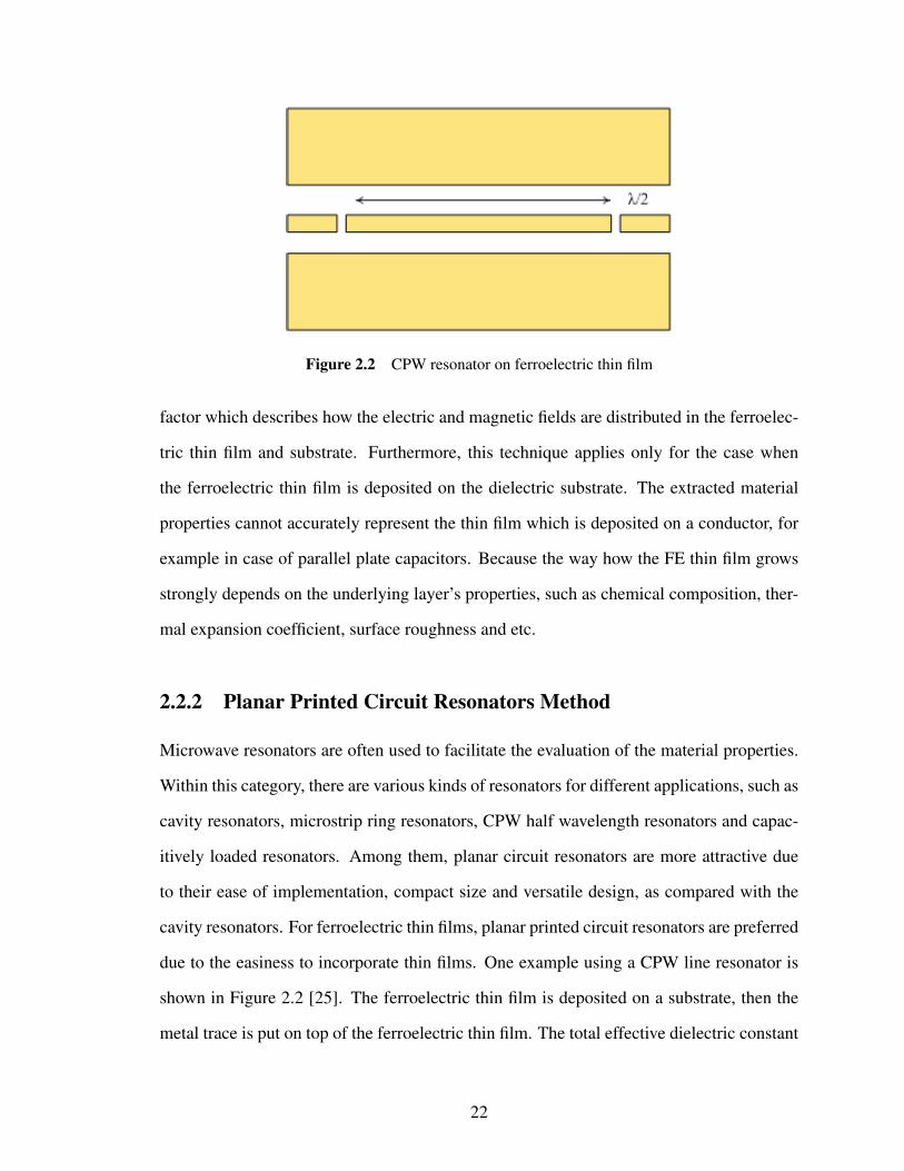
Figure 2.2 CPW resonator on ferroelectric thin film
factor which describes how the electric and magnetic fields are distributed in the ferroelec-
tric thin film and substrate. Furthermore, this technique applies only for the case when
the ferroelectric thin film is deposited on the dielectric substrate. The extracted material
properties cannot accurately represent the thin film which is deposited on a conductor, for
example in case of parallel plate capacitors. Because the way how the FE thin film grows
strongly depends on the underlying layer’s properties, such as chemical composition, ther-
mal expansion coefficient, surface roughness and etc.
2.2.2 Planar Printed Circuit Resonators Method
Microwave resonators are often used to facilitate the evaluation of the material properties.
Within this category, there are various kinds of resonators for different applications, such as
cavity resonators, microstrip ring resonators, CPW half wavelength resonators and capac-
itively loaded resonators. Among them, planar circuit resonators are more attractive due
to their ease of implementation, compact size and versatile design, as compared with the
cavity resonators. For ferroelectric thin films, planar printed circuit resonators are preferred
due to the easiness to incorporate thin films. One example using a CPW line resonator is
shown in Figure 2.2 [25]. The ferroelectric thin film is deposited on a substrate, then the
metal trace is put on top of the ferroelectric thin film. The total effective dielectric constant
22

of the CPW resonator is determined by (2.16)
εe f f = (c
2 f0l)2 (2.16)
where c is the speed of light in vacuum, f0 is the resonance frequency of the CPW
resonator, l is the length of the resonator. By applying a similar analysis using conformal
mapping as described in previous section, the permittivity of the ferroelectric thin film can
be calculated by (2.4).
From the resonant frequency f0 and the 3 dB bandwidth ∆ f , the effective dielectric loss
tangent is obtained by (2.17)
tanδ =2∆ f
f0(2.17)
As before substrate and radiation loss are negligible here. Therefore the effective loss
tangent is due to the ferroelectric thin film dielectric loss and the conductor loss. Same
analysis as in the previous case can be used to extract the true dielectric loss tangent of thin
film ferroelectrics. An alternative way is to use superconductor, such as YBCO. In this case
the conductor loss can be assumed to be zero.
In conclusoin the measurement technique based on planar circuit resonators is very sim-
ple in the implementation and post-measurement data process, and it is accurate. However
a main drawback is that this technique applies only to a single frequency. It’s impossible to
characterize the material in a broad frequency range using this characterization method.
2.2.3 Capacitors Method
Ferroelectric thin films have been under active research for decades for the applications
from high density DRAM, non-volatile computer memory (FeRAM), high-K gate transis-
tors and tunable microwave circuits. In all these applications, the fundamental component
is a capacitor in forms of either parallel plate or interdigital. Therefore, capacitors are a
23
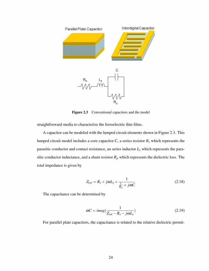
Figure 2.3 Conventional capacitors and the model
straightforward media to characterize the ferroelectric thin films.
A capacitor can be modeled with the lumped circuit elements shown in Figure 2.3. This
lumped circuit model includes a core capacitor C, a series resistor Rs which represents the
parasitic conductor and contact resistance, an series inductor Ls which represents the para-
sitic conductor inductance, and a shunt resistor Rp which represents the dielectric loss. The
total impedance is given by
Ztot = Rs + jωLs +1
1Rp
+ jωC(2.18)
The capacitance can be determined by
ωC = imag(1
Ztot −Rs− jωLs) (2.19)
For parallel plate capacitors, the capacitance is related to the relative dielectric permit-
24
tivity (εr), electrode area (A) and dielectric thickness (d) by
C =ε0εrA
d(2.20)
The total quality factor (Q factor) can be directly calculated by
Qtot =imag(Ztot)real(Ztot)
(2.21)
and the loss tangent is determined by (2.22) assuming that the parasitics Rs and Ls are
known.
tanδ =− real(Ztot −Rs− jωLs)imag(Ztot −Rs− jωLs)
(2.22)
2.3 Modeling of Parallel Plate Capacitors
A simple structure for a parallel plate capacitor consists of three layers: a bottom metal
electrode, a ferroelectric thin film and a top metal electrode. The two metal electrodes
exhibit the parasitic resistance and inductance which lower the total Q-factor and self res-
onance frequency. The parasitic resistance increases as the operation frequency increases
due to the skin depth effect. Therefore in order to extract the material loss tangent accu-
rately, the effect of the electrodes must be studied and modeled carefully.
A first-thought estimation of the electrodes resistance is equal to the RF resistance of
the electrodes by
Rs =L
σWt(2.23)
where σ is the metal conductivity, and L, W and t are the length,width and thickness of
the electrode. However this is wrong! This calculation is valid under the condition that the
current density on the electrode is uniform. In parallel plate capacitors, it is interestingly
25
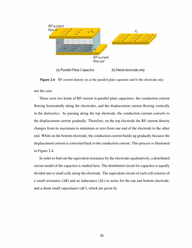
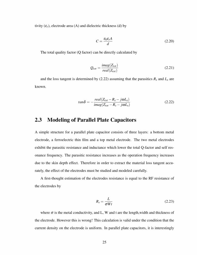
Figure 2.4 RF current density on a) the parallel plate capacitor and b) the electrode only
not the case.
There exist two kinds of RF current in parallel plate capacitors: the conduction current
flowing horizontally along the electrodes, and the displacement current flowing vertically
in the dielectrics. As passing along the top electrode, the conduction current converts to
the displacement current gradually. Therefore, on the top electrode the RF current density
changes from its maximum to minimum or zero from one end of the electrode to the other
end. While on the bottom electrode, the conduction current builds up gradually because the
displacement current is converted back to the conduction current. This process is illustrated
in Figure 2.4.
In order to find out the equivalent resistance by the electrodes qualitatively, a distributed
circuit model of the capacitor is studied here. The distributed circuit for capacitor is equally
divided into n small cells along the electrode. The equivalent circuit of each cell consists of
a small resistance (∆R) and an inductance (∆L) in series for the top and bottom electrode,
and a shunt small capacitance (∆C), which are given by
26
Figure 2.5 Circuit model of parallel plate capacitors
Figure 2.6 Simplified circuit model of parallel plate capacitors
∆R =R′
n(2.24)
∆L =L′
n(2.25)
∆C =Ctot
n+1(2.26)
where R′and L
′are the resistance and inductance of the electrode with uniform current
density, and Ctot is the total capacitance given by (2.20). The distributed circuit model is
shown in Figure 2.5. Since top and bottom electrodes present equal parasitics, a simplified
distributed circuit model with the bottom electrode only is shown in Figure 2.6.
This circuit is indeed a transmission line loaded with an open circuit at one end. Using
27

the tranditional transmission line theory, the propagation constant and the characteristic
impedance are given by
γ =√
zy =√
(∆R+ jω∆L) jω∆C (2.27)
Z0 =√
zy
=
√∆R+ jω∆L
jω∆C(2.28)
where z is the series impedance and y is the shunt admittance per unit length. The input
impedance of an open circuited transmission line with length L is given by
Zin = Z0coth(γL) (2.29)
Using the Laurent series expansion, (2.29) can be approximated to
Zin ≈ Z0(1
γL+
γL3
) (2.30)
With (2.25) and (2.26), the input impedance of the capacitor is derived as (2.31)
Zin ≈ R′+ jωL
′
3+
1jωCtot
(2.31)
From (2.31), the contribution due to the top electrode is only 1/3 of the impedance of a
same size metal piece. The bottom electrode will have the same impedance as the top elec-
trode. Therefore the total parasitic impedance of the electrodes in parallel plate capacitors
has a scaling factor of 2/3, which is the same as reported in [26].
28

2.4 De-embedding Techniques of Parallel Plate Capaci-tors
In the on wafer microwave characterization, modeling and de-embedding of the parasitics
are an important and difficult task in order to retrieve the real performance of the device
under test (DUT) which has to be embedded in a ’probe friendly’ structure. For the parallel
plate capacitors using ferroelectric thin films, these parasitics are originated from:
• Probe contact pads
• Interconnecting circuitries from probe contact pads to the capacitors
• Any discontinuity
• Top and bottome electrodes
• Probe contact resistance
The standard calibration methods like short-open-load-through (SOLT) and through-
reflection-line (TRL) calibrate the reference plane up to the probe tips, removing all the
effects from equipments and cables. However they are insufficient to de-embed the above
parasitics. With the introduction of some additional on-wafer structures, the real material
properties of ferroelectric thin films can be extracted.
2.4.1 One Port Measurement Technique Using Signal-Ground (SG)Probes
There are a total of three kinds of structure fabricated on the same wafer: the parallel
plate capacitors, and two short standards with different lengths [23]. Their physical layouts
and the lumped circuit models are shown in Figure 2.7. They can be modeled as a series
impedance individually, Zs1 for short standard 1, Zs2 for short standard 2 and Zmc for the
unde-embedded capacitor. The input impedance of these three structures can be obtained
29

Figure 2.7 Physical layouts and circuit models for one port measurement using SG probe
from one port reflection coefficient S11 by
Zin = Z01+S11
1−S11(2.32)
and
Zs1 = R1 + jωL1 (2.33)
Zs2 = R2 + jωL2 (2.34)
Zmc = R1 + jωL1 +Re + jωLe +1
Gd + jωC(2.35)
Zs1 represents the parasitics due to the probe pads, interconnection lines and the discon-
tinuity between them. By subtracting Zs1 from Zs2, the impedance of line having the same
length and width as the capacitor electrodes can be obtained. The parasitic impedance due
to the electrodes (Re + jωLe) is equal to 23 of the difference between Zs1 and Zs2, as shown
in the previous section. With the knowledge of all these parastics, the capacitor impedance
30
can be calculated by
Zc = Zmc−Zs1− 23(Zs2−Zs1) (2.36)
Consequently the loss tangent and capacitance are given by
tanδ =1
Gd jωC=− real(Zc)
imag(Zc)(2.37)
C =− 1imag(Zc)ω
(2.38)
However the accuracy of the SG probe diminishes at high microwave frequencies due to
unbalanced field termination at the probe tip. Instead, ground-signal-ground (GSG) probes
are more accurate for high frequency on wafer measurements.
2.4.2 One Port Measurement Technique Using GSG Probes
Coplanar waveguide (CPW) probe structure is used to embed the DUT when the GSG
probe is used for measurement. In addition to the series parasitic impedance, there is a
shunt parastic admittance between the signal line and the two ground pads, as shown in
Figure 2.8. To de-embed them, two additional standards are needed in which the DUT
is replaced by an open or a short circuit [27]. The de-embed procedures are summerized
below.
1. Measure the DUT, the short and open standards using GSG probe with the net-
work analyzer. Using (2.32), convert the measured one port reflection coefficients to the
respective input impedances Zmeas, Zshort and Zopen.
2. The series parasitic impedance Zs is equal to Zshort .
31

Figure 2.8 Physical layout and circuit model for one port measurement using GSG probes
3. Subtract Zopen from Zshort , the shunt parasitic admittance Yp is obtained by
Yp =1
Zopen−Zshort(2.39)
4. Finally the DUT impedance ZDUT is calculated by
ZDUT =1
1Zmeas−Zs
−Yp(2.40)
By applying this de-embed procedure to capacitors, short standard 1 and 2, then using
(2.33) - (2.38), one can extract loss tangent and capacitance for capacitors.
2.4.3 Two Port Measurement Technique Using GSG Probes
The impedance of high Q-factor capacitors is approximately equal to Rs + jωC. When the
parasitic resistance is much smaller than the reactance, the magnitude of the reflection coef-
ficient is close to 1. The network analyzer has a larger uncertainty in the measured reflection
coefficient for unmatched loads (|S11| = 1) than matched loads (|S11| = 0). Furthermore,
32

Figure 2.9 Physical layout and circuit model for two port measurement using GSG probes
the conversion for S11 to input impedance Zin using (2.32) in the one port measurement
technique is sensitive to the measurement error in S11 because the denominator is close to
zero when |S11|= 1. Therefore, a two port measurement technique is presented in order to
improve the measurement accuracy [28].
In a two port measurement setup, two GSG probes are used to measure the capaci-
tors, standard 1 and 2 in CPW structures, as shown in Figure 2.9. Similar to the one port
configuration using GSG probes, there are both series and shunt parasitics in the two port
structures. Instead of using additional short and open circuit standards to de-embed these
parasitics as is done in the one port technqiue using GSG probes, the impedance of the
DUT can be extracted by converting the two port S-parameters to ABCD parameters. For
the two port configuration, the corresponding ABCD matrix is given by
∣∣∣∣∣∣∣A B
C D
∣∣∣∣∣∣∣=
∣∣∣∣∣∣∣1 0
Yp 1
∣∣∣∣∣∣∣
∣∣∣∣∣∣∣1 ZDUT
0 1
∣∣∣∣∣∣∣
∣∣∣∣∣∣∣1 0
Yp 1
∣∣∣∣∣∣∣=
∣∣∣∣∣∣∣1+YpZDUT ZDUT
2Yp +Y 2p ZDUT 1+YpZDUT
∣∣∣∣∣∣∣
33

The B parameter is equal to the impedance of the DUT which includes the series par-
asitics such as, probe pads and interconnects. After calculating the B parameters for the
capacitor, line standard 1 and 2 by using (2.41)
ZDUT = B = Z0(1+S11)(1+S22)−S12S21
2S21(2.41)
The loss tangent and the capacitance of the ferroelectric thin film capacitors can be
determined by using (2.33) - (2.38).
In two port S-parameter measurement, the reflection coefficient at both ports are mea-
sured with the other port terminated with the system characteristic impedance Z0 of the
network analyzer, which is normally equal to 50 Ω. Therefore, for high Q-factor capaci-
tors, both S11 and S22 are close to zero instead of 1 in the one port measurement technique.
With S21 and S12 are close to 1, (2.41) is not sensitive to the measured s-parameters’ er-
rors. As a result, the two port measurement technique is more accurate than the one port
reflection technique. A detailed uncertainty analysis of both techniques will be presented
to verify this in the next section.
2.5 Uncertainty Study
For a function y dependent on a number of measured quantities xi, the uncertainty is calcu-
lated by (2.42)[29] under the assumption that xi are uncorrelated.
δyy
=
(∑
i
(δxi
xi
)2 (Sy
xi
)2
)0.5
(2.42)
where
Syxi
=xi
y∂y∂xi
(2.43)
In characterizing BST thin films, the final extracted quantities such as loss tangent and
the capacitance or dielectric constant, are obtained from the measured one port or two port
34

S-paramters. Therefore, the uncertainty of the loss tangent and the capacitance is related
to the uncertainty of the measured S-paramters through (2.42-2.43). The uncertainty of
the S-paramters measured by the network analyzer are provided by the manufacturer [30].
By lowering the IF bandwidth and increasing the average factor, the uncertainty of the
S-parameters can be minimized, as shown in Figure 2.10 and 2.11.
In one port measurement technique, the loss tangent and the capacitance are determined
by (2.32-2.38). Then by applying (2.42, 2.43) to (2.37, 2.38), the uncertainty of the loss
tangent and the capacitance are derived to be:
∆tanδtanδ
=1
tanδ
[∆|S11|2
( |S11|2 +12|S11|2sinφ11
)2
+(∆φ11)2(
1−|S11|22|S11|sin2φ11
cosφ11
)2]1/2
(2.44)
∆CC
=Y0
ωCA+B2 (2.45)
where
A = (∆|S11|)2
[2sinφ11−2|S11|2cosφ11
(1+2|S11|cosφ11 + |S11|2)2
]2
(2.46)
B = (∆φ11)2
[2|S11|cosφ11 +4|S11|2 +2|S11|3cosφ11
(1+2|S11|cosφ11 + |S11|2)2
]2
(2.47)
where |S11| and ∆φ11 are the measured S11 magnitude and phase, ∆|S11| and ∆φ11 are
the error of the magnitude and phase of the reflection coefficient, Y0 is characteristic admit-
tance, and ω is the angular frequency.
From (2.44), it is clear that the uncertainty of the extracted loss tangent comes from two
parts: error in the magnitude and phase of S11. Since the error from the phase is negligible
35
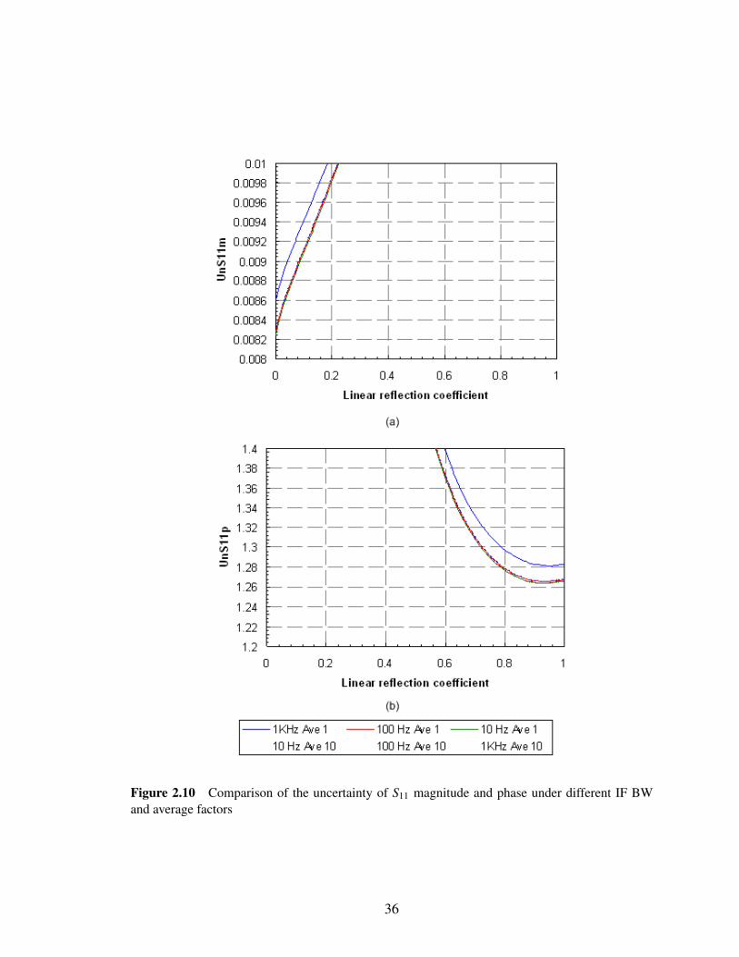
Figure 2.10 Comparison of the uncertainty of S11 magnitude and phase under different IF BWand average factors
36

Figure 2.11 Comparison of the uncertainty of S21 magnitude and phase under different IF BWand average factors
37
compared with that from the magnitude, (2.44) can be rewrited as
∆tanδtanδ
∼= 1tanδ
(∆|S11|
( |S11|2 +12|S11|2sinφ11
))(2.48)
Since S11 is close to 1 for BST varactors measured by one port measurement technique,
the minimum value of the term in parentheses is equal to 1, as given in (2.49).
min( |S11|2 +1
2|S11|2sinφ11
)= 1 (2.49)
Thus the minimum uncertainty of the loss tangent is determined solely by the actual
dielectric loss tangent and the error of the magnitude of the reflection coefficient which is
set by the network analyzer in the setup, by
∆tanδtanδ
∼= 1tanδ
∆|S11| (2.50)
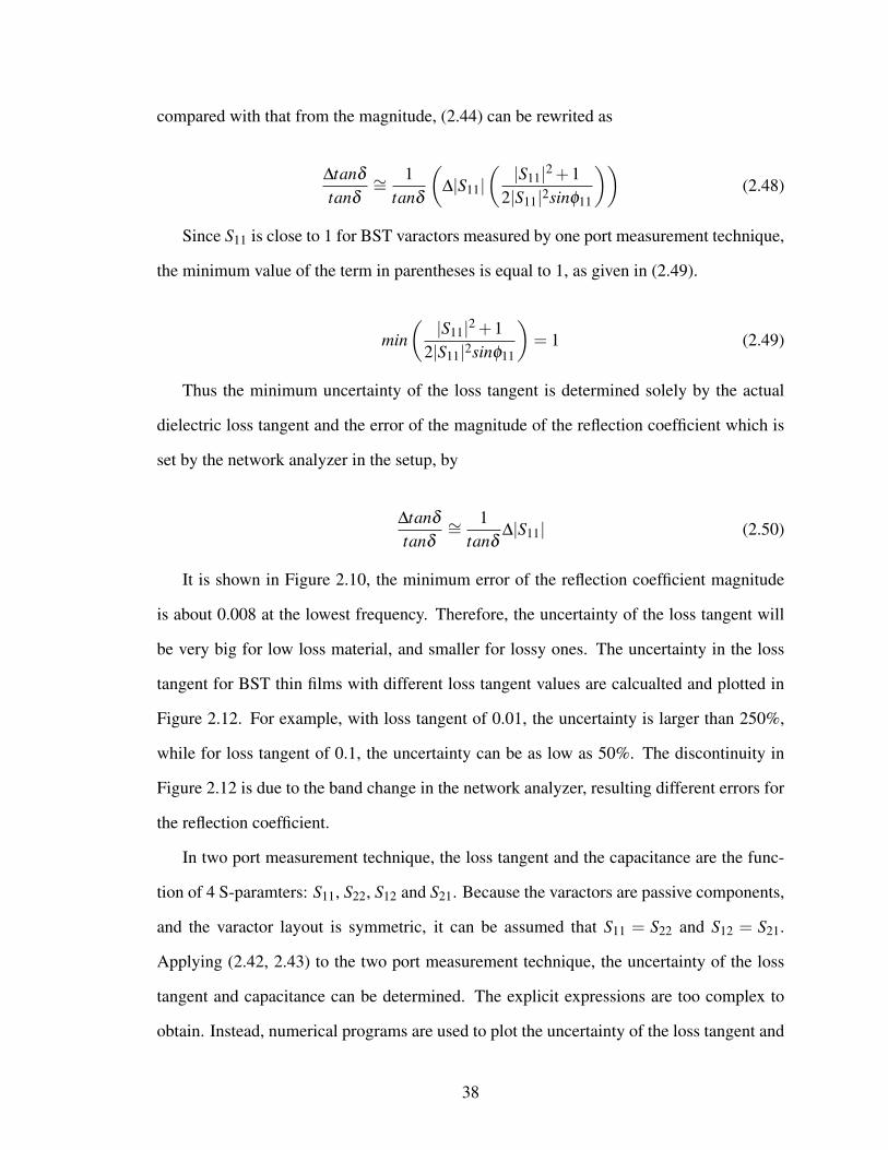
It is shown in Figure 2.10, the minimum error of the reflection coefficient magnitude
is about 0.008 at the lowest frequency. Therefore, the uncertainty of the loss tangent will
be very big for low loss material, and smaller for lossy ones. The uncertainty in the loss
tangent for BST thin films with different loss tangent values are calcualted and plotted in
Figure 2.12. For example, with loss tangent of 0.01, the uncertainty is larger than 250%,
while for loss tangent of 0.1, the uncertainty can be as low as 50%. The discontinuity in
Figure 2.12 is due to the band change in the network analyzer, resulting different errors for
the reflection coefficient.
In two port measurement technique, the loss tangent and the capacitance are the func-
tion of 4 S-paramters: S11, S22, S12 and S21. Because the varactors are passive components,
and the varactor layout is symmetric, it can be assumed that S11 = S22 and S12 = S21.
Applying (2.42, 2.43) to the two port measurement technique, the uncertainty of the loss
tangent and capacitance can be determined. The explicit expressions are too complex to
obtain. Instead, numerical programs are used to plot the uncertainty of the loss tangent and
38

Figure 2.12 Comparison of the uncertainty in the loss tangent for BST thin films with differentloss tangent values using one port measurement technique.
Figure 2.13 Comparison of uncertainty of loss tangent using one port and two port measurementtechniques
the capacitance determined by two port measurement technique.
It is shown in Figure 2.13 and 2.14 that the two port measurement technique is more
accurate than the one port measurement technique, with 30% improvement of uncertainty
39

Figure 2.14 Comparison of uncertainty of capacitance using one port and two port measurementtechniques
in both loss tangent and capacitance. Therefore, for characterization of ferroelectric thin
films and varactors at the microwave frequency, the two port measruement technique is
recommended because it is not only simpler to implement but also more accurate than
conventional one port reflection type measurement technique.
2.6 Measurement Results
The two port measurement technique has been applied to the BST tunable capacitors. It is
shown in Figure 2.15 that without the proper de-embed technique, the extracted loss tan-
gent of BST thin films is erroneously larger than its real value. The extracted loss tangent,
permittivity of BST thin films are shown in Figure 2.16 and 2.17.
40

Figure 2.15 Comparison of loss tangent with/without de-embeding using two port measurementtechnique
2.7 Conclusion
Commonly used measurement and deembedding techniques to characterize ferroelectric
thin films and varactors are discussed in this chapter. CPW structures are not suitable for
characterization of parallel plate capacitors because the deposited ferroelectric thin film
exhibits different material and electrical properties with or without metal bottom electrode.
Instead, measurements of capacitors are a straightforward way. The conventional one port
reflection type measurement technique is not accurate because the S11 of low loss capacitors
measured from the network analyzer is very sensitive to the errors. A two port measure-
ment technique is proposed to provide not only an easier deembedding process but also
better acuracy. The uncertainty study of both techniques shows that two port measurement
technique improves the uncertainty of the extracted loss tangent and capacitance by 30%.
41
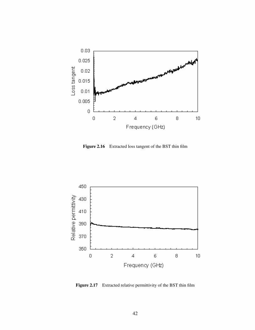
Figure 2.16 Extracted loss tangent of the BST thin film
Figure 2.17 Extracted relative permittivity of the BST thin film
42
Chapter 3
FABRICATION OF FERROELECTRIC THIN FILM VARACTORSAND THEIR APPLICATION IN MICROWAVE TUNABLE
CIRCUITS
In this chapter, fabrication of ferroelectric thin film varactors and their application in mi-
crowave tunable circuits are discussed in details. The fabrication process includes the thin
film deposition optimization and the clean room fabrication process. Pulsed laser depo-
sition technique (PLD) is used to deposit ferroelectric thin films. Thin film deposition
parameters are studied and optimized in order to achieve good quality BST thin films for the
design of microwave varactors. The goal is to fabricate BST thin films with a low loss tan-
gent and a high permittivity tunability. A full clean room fabrication process is developed.
Various microwave tunable circuits are demonstrated using this fabrication process.
3.1 Optimization of Ferroelectric Thin Films Depositedby Pulsed Laser Deposition
As the semiconductor industry advances, thin film deposition techniques become more
and more mature. Ferroelectric thin films have been successfully deposited by various
deposition methods: molecular beam epitaxy (MBE) [31], metal-organic chemical vapor
deposition (MOCVD) [23, 32], sol-gel [33], RF sputtering [16] and pulsed laser deposition
(PLD) [34]. It is difficult to choose one as the best technique because each has its own
merits and limits depending on the application in mind and the available budget. In this
work PLD process is used because of its advantages such as:
• Maintaining stoichiometry of deposited thin films as the target material
43

• High deposition rate (about 10 nm/min)
• Low process temperature (about 600 °C)
• Multi-material deposition without breaking the chamber vacuum
• Low cost multi-chamber deposition using one laser source
On the other hand, PLD process suffers from shortcomings such as:
• Nonuniform thin films
• Small useful deposition areas (1cm by 1cm)
• Particulate and defects
• Target surface modification due to the laser ablation
Techniques like mechanical particle filter and substrate rotation can be used to decrease
the number of small particulate and to improve the film uniformity at the expense of the
deposition rate. In general, PLD is more favorable for academic and laboratory research as
opposed to industry manufacturing.
3.1.1 Pulsed Laser Deposition Process
Pulsed laser deposition, as implied by its name, utilizes a laser to deposit thin films. The
setup of PLD is quite simple, as shown in Figure 3.1. It consists of a laser source, a vacuum
chamber and a gas pressure and substrate temperature control system. Inside the vacuum
chamber, there exist a target mount and a temperature controlled substrate. Though the
physical process and mechanics of PLD process are very complicated and are subject of
on-going research, they can be briefly described as:
• A focused high energy density laser (1 - 2J/cm2) hits the rotating target material
• The laser energy causes the ablation and evaporation process on the target surface
• The ablated target materials in the forms of electrons, ions, neutrals and ionized
species form an ionized plasma plume
• The plume interacts with the ambient reactive gas.
• The plume reaches the heated substrate and deposits the target material on it.
44

Figure 3.1 Illustration of a typical PLD setup.
3.1.2 Deposition Parameter Optimization
In PLD process, the deposited thin film quality is strongly dependent on the deposition pa-
rameters such as substrate temperature, reactive gas pressure, laser fluence and post process
annealing. By varying each parameter, BST thin films are deposited and studied. Parallel
plate capacitors are then fabricated and measured using two port measurement technique
described in chapter 2 to extract the BST loss tangent, permittivity under different DC bias
voltage. Sapphire is used as the substrate because it presents a very low loss at microwave
frequencies and its thermal expansion coefficient (CTE) is close that of BST thin films.
Both the bottom and top electrode are made of platinum because platinum has a similar
CTE to BST thin films and it has high conductivity. The BST target is a 2 inch high purity
Ba0.5Sr0.5TiO3 ceramic disk.
The effect of substrate temperature on the performance of BST thin films
The substrate temperature plays an important role in determining the crystalline quality of
the BST thin film by affecting the adatom’s mobility. From low temperature to high temper-
ature, the crystalline phase usually varies from amorphous, to polycrystalline and to highly
45

Figure 3.2 C-V tuning curves for BST thin films deposited at 500, 600 and 700 degrees
oriented thin films. Usually BST thin films with a better crystalline quality can achieve a
better tunability. Therefore high substrate temperature is desired for highly tunable BST
thin films. On the other hand, it is reported that higher loss is unfortunately associated
with the higher tunability in BST thin films, thus degrading the device Q-factor [35]. This
may be due to the strain caused by the thermal mismatch between the BST thin film and
the underneath electrode and substrate. In some cases, the large thermal mismatch due to
the high substrate temperature causes cracks/peelings in the deposited thin films during the
cooling phase.
BST thin films are deposited at three different substrate temperatures: 500 °C , 600 °C
and 700 °C with all the other deposition parameters kept the same. It’s found that 500 °C
BST thin films can be barely tuned. As the temperature increased to 600 °C and 700 °C,
the tunability is increased to 2:1 and 3:1 respectively, as shown in Figure 3.2.
46
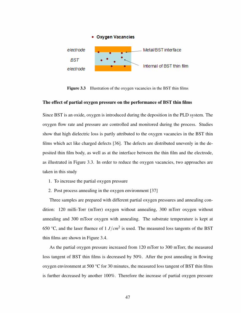
Figure 3.3 Illustration of the oxygen vacancies in the BST thin films
The effect of partial oxygen pressure on the performance of BST thin films
Since BST is an oxide, oxygen is introduced during the deposition in the PLD system. The
oxygen flow rate and pressure are controlled and monitored during the process. Studies
show that high dielectric loss is partly attributed to the oxygen vacancies in the BST thin
films which act like charged defects [36]. The defects are distributed unevenly in the de-
posited thin film body, as well as at the interface between the thin film and the electrode,
as illustrated in Figure 3.3. In order to reduce the oxygen vacancies, two approaches are
taken in this study
1. To increase the partial oxygen pressure
2. Post process annealing in the oxygen environment [37]
Three samples are prepared with different partial oxygen pressures and annealing con-
dition: 120 milli-Torr (mTorr) oxygen without annealing, 300 mTorr oxygen without
annealing and 300 mToor oxygen with annealing. The substrate temperature is kept at
650 °C, and the laser fluence of 1 J/cm2 is used. The measured loss tangents of the BST
thin films are shown in Figure 3.4.
As the partial oxygen pressure increased from 120 mTorr to 300 mTorr, the measured
loss tangent of BST thin films is decreased by 50%. After the post annealing in flowing
oxygen environment at 500 °C for 30 minutes, the measured loss tangent of BST thin films
is further decreased by another 100%. Therefore the increase of partial oxygen pressure
47

Figure 3.4 Loss tangent of the BST thin films under different partial oxygen pressure and anneal-ing conditions
and post process oxygen annealing are very effective to reduce the dielectric loss at the
microwave frequencies.
The effect of laser fluence on the performance of BST thin films
The laser fluence, or the laser power density, is another important parameter in PLD pro-
cess. It is defined as the laser power on the material target surface per unit area, given by
(3.1)
laser f luence =Out put laser power
laser spot area on target(J/cm2) (3.1)
Sufficient laser fluence is needed to ablate the target materials while keeping the ma-
terial’s stoichiometry. The laser fluence can be adjusted by either varying the output laser
power or the laser spot area on the target through an external optics system. A smaller
spot size of the focused laser beam is preferred because the required output laser power is
smaller, thus laser lifetime can be increased.
48
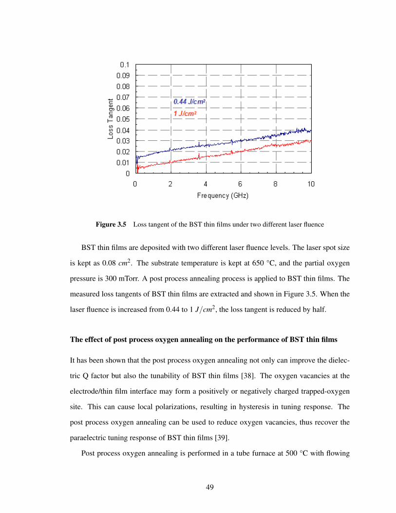
Figure 3.5 Loss tangent of the BST thin films under two different laser fluence
BST thin films are deposited with two different laser fluence levels. The laser spot size
is kept as 0.08 cm2. The substrate temperature is kept at 650 °C, and the partial oxygen
pressure is 300 mTorr. A post process annealing process is applied to BST thin films. The
measured loss tangents of BST thin films are extracted and shown in Figure 3.5. When the
laser fluence is increased from 0.44 to 1 J/cm2, the loss tangent is reduced by half.
The effect of post process oxygen annealing on the performance of BST thin films
It has been shown that the post process oxygen annealing not only can improve the dielec-
tric Q factor but also the tunability of BST thin films [38]. The oxygen vacancies at the
electrode/thin film interface may form a positively or negatively charged trapped-oxygen
site. This can cause local polarizations, resulting in hysteresis in tuning response. The
post process oxygen annealing can be used to reduce oxygen vacancies, thus recover the
paraelectric tuning response of BST thin films [39].
Post process oxygen annealing is performed in a tube furnace at 500 °C with flowing
49

Figure 3.6 C-V tuning curves of the BST thin film (a) without and (b) with the post processoxygen annealing
50
oxygen for 30 minutes. The BST thin film is deposited at 650 °C, 300 mTorr partial oxygen
pressure, and the laser fluence of 1 J/cm2. In the tunability measurement, the DC bias volt-
age is swept from -10 V to 10 V, then back to -10 V. This DC bias sweep scheme is repeated
for several times. Without the post process oxygen annealing, the measured C-V response
is asymmetric about 0V as shown in Figure 3.6 (a). The capacitances for forward (-10 V to
10 V) bias are different than the capacitances for backward (10 V to -10 V) bias. This can
be attributed to a built-in voltage potential existed at the electrode-thin film interface. After
the post process oxygen annealing, the normal paraelectric response of the Ba0.5Sr0.5TiO3
thin film is recovered as shown in Figure 3.6 (b).
After the deposition conditions are studied and optimized, a PLD process to achieve
high Q-factor microwave varactor using BST thin films is summarized below:
• Substrate temperature of 650 °C.
• Partial oxygen pressure of 300 mTorr.
• Laser fluence of 1 J/cm2
• Post process oxygen annealing at 500 °C, flowing oxygen environment for 30 min-
utes.
BST varactors are measured to achieve Q-factors above 100 in the lower GHz range
with this PLD process as shown in Figure 3.7. The deposited BST thin films are polycys-
talline thin films with a < 111 > preferred orientation. The measured X-ray diffraction
(XRD) is shown in Figure 3.8.
3.2 Clean Room Fabrication Process
All the fabrication is carried out in the Michigan Lurie Nanofabrication Facility under class
1000/100 clean room environment. There are more than 10 steps for the fabrication of fer-
roelectric thin film based tunable capacitors and circuits. The graphic illustration of the
fabrication flow is shown in Figure 3.9. The substrate used is a single side polished 430
51
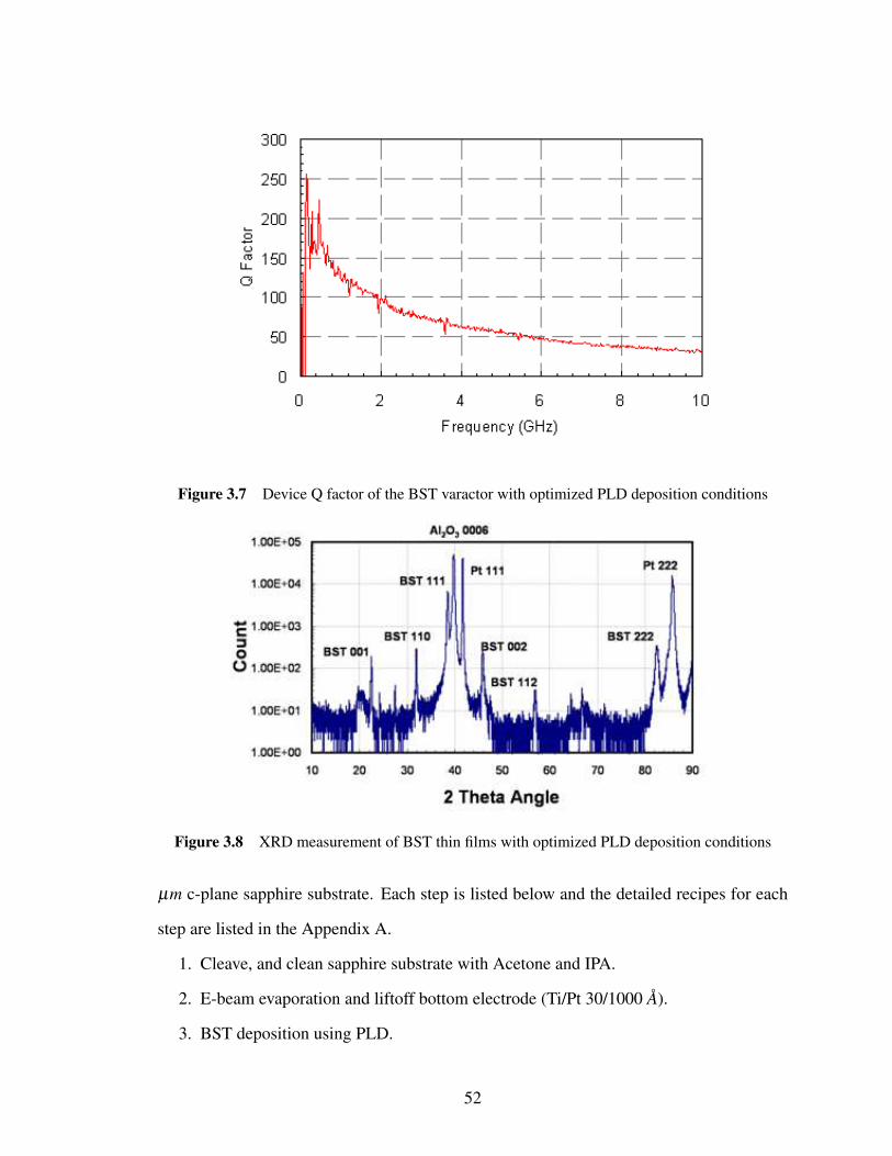
Figure 3.7 Device Q factor of the BST varactor with optimized PLD deposition conditions
Figure 3.8 XRD measurement of BST thin films with optimized PLD deposition conditions
µm c-plane sapphire substrate. Each step is listed below and the detailed recipes for each
step are listed in the Appendix A.
1. Cleave, and clean sapphire substrate with Acetone and IPA.
2. E-beam evaporation and liftoff bottom electrode (Ti/Pt 30/1000 A).
3. BST deposition using PLD.
52

Figure 3.9 Process flow of ferroelectric thin film based varactors and circuits
4. Etching silver paint by the gold etchant.
5. E-beam evaporation and liftoff top electrode (Pt 1000 A).
6. Post process annealing.
7. Patterning BST thin film using diluted HF solution (HF:DI water 1:10).
8. DC sputter and liftoff high resistivity SiCr thin film (700 A).
9. E-beam evaporation and liftoff contacts (Ti/Au 50/3000 A).
10. SiO2 passivation using PECVD and wet etching in BHF (5000 A).
11. E-beam evaporation and liftoff circuitry seed layer (Ti/Au 50/5000 A).
12. Gold plating to 10 µm.
13. Seed layer etch back.
14. Dice off devices (option).
53
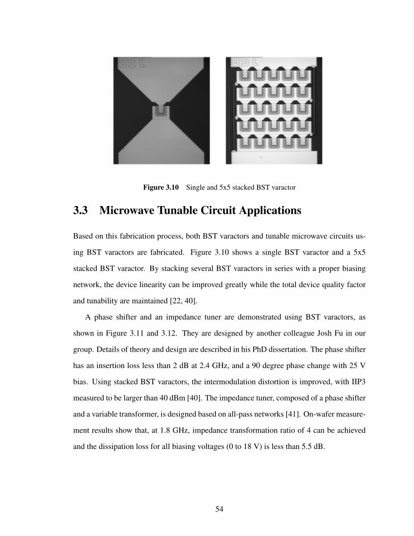
Figure 3.10 Single and 5x5 stacked BST varactor
3.3 Microwave Tunable Circuit Applications
Based on this fabrication process, both BST varactors and tunable microwave circuits us-
ing BST varactors are fabricated. Figure 3.10 shows a single BST varactor and a 5x5
stacked BST varactor. By stacking several BST varactors in series with a proper biasing
network, the device linearity can be improved greatly while the total device quality factor
and tunability are maintained [22, 40].
A phase shifter and an impedance tuner are demonstrated using BST varactors, as
shown in Figure 3.11 and 3.12. They are designed by another colleague Josh Fu in our
group. Details of theory and design are described in his PhD dissertation. The phase shifter
has an insertion loss less than 2 dB at 2.4 GHz, and a 90 degree phase change with 25 V
bias. Using stacked BST varactors, the intermodulation distortion is improved, with IIP3
measured to be larger than 40 dBm [40]. The impedance tuner, composed of a phase shifter
and a variable transformer, is designed based on all-pass networks [41]. On-wafer measure-
ment results show that, at 1.8 GHz, impedance transformation ratio of 4 can be achieved
and the dissipation loss for all biasing voltages (0 to 18 V) is less than 5.5 dB.
54
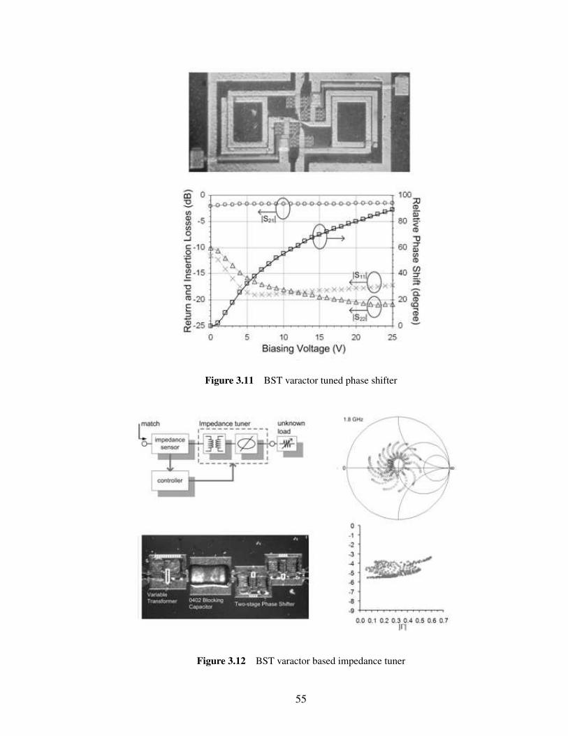
Figure 3.11 BST varactor tuned phase shifter
Figure 3.12 BST varactor based impedance tuner
55

3.4 Conclusion
Deposition of BST thin films using PLD system has been studied. The deposition con-
ditions are optimized in order to achieve microwave varactors with high Q-factor and
moderate tunability. The substrate temperature, partial oxygen pressure, laser fluence and
post process oxygen annealing are found to have major impacts on the deposited BST thin
films electrical properties such as loss tangent, relative permittivity and tunability. High
Q-factor microwave varactors have been fabricated with the optimized PLD conditions.
A clean room fabrication process is developed. BST varactors and tunable circuits are
demonstrated with this fabrication process.
56

Chapter 4
TUNABLE MICROWAVE FILTER USING BST VARACTORS
4.1 Introduction
Filters are indispensable in modern communication systems where accurate spectral control
is needed. Tunable filters, especially, are becoming more desirable in the rapidly growing
wireless communication industry, where mobile devices capable of operating over different
frequency bands are of great interest. Novel tunable devices are needed for the design of
such tunable filters. RF microelectro-mechanical systems (MEMS) and thin film ferroelec-
tric varactors are two promising technologies that are currently under investigation. RF
MEMS filters have been studied for continuously tuning mode [42] and digital-type tuning
mode [43]. However, MEMS varactors suffers from large bias voltages (30 to 50 volts)
and slow tuning speed in the range of 1-300 µsec [1]. Ferroelectric based varactors have
several merits, for example, lower tuning voltage (5 to 10 volts), fast response speed (ap-
proximate ns) and good quality factor [16]. Several works on tunable combline filters using
ferroelectric varactors have been reported. In [44], thick BST film was used to form gap
capacitors; while in [45] interdigital type capacitors were employed. Both of them asked
for very large bias voltage because of poor usage of the tuning field. Filters employing par-
allel plate capacitor need much lower tuning voltage [46]. In this chapter, a fully integrated
2 GHz 3 pole tunable filter using BST varactors is presented with the design, fabrication
and measurement results.
57

Zin
λ/2
(a)
Zin
λ/4
(b)
Zin
ϑ < λ/4
(d)
CT
CT
(c)
ϑ < λ/2
Zin
Figure 4.1 (a) Half wavelength, (b) quarter wavelength, (c) capacitvely loaded quarter wavelengthand (d) capacitively loaded ring resonator
4.2 Capacitively Loaded Ring Resonators
Coupled resonator filters are commonly used in RF/microwave systems, especially in
narrow-band bandpass filters applications. Two of the basic resonator structures are quarter-
wave and half-wave transmission line resonators. In order to reduce the resonator’s size,
capacitors can be used to load the transmission line. The need of via holes not only com-
plicates the fabrication but also introduces parasitics that cause extra loss and detune the
resonance frequency. Instead, a capacitively loaded ring resonator is used with no need of
vias as in Figure 4.1.
Four types of transmission line resonators are analyzed here. They are half wave-
length resonators, quarter wavelength resonators, capacitively loaded quarter wavelength
resonators and capacitively loaded ring resonators. The magnitude of input impedances of
these four resonators are plotted as shown in Figure 4.2. All of the resonators have the shunt
resonance at 1.8 GHz which results from an impedance pole. Both quarter-wave resonator
and capacitively loaded ring resonator present an additional zero in contrast to quarter-wave
and capacitively loaded quarter-wave resonator. The relative distance from the zero to the
pole of resonators determines how sharp the filter’s out-of-band rejection will be. Thus,
the closer the zero to the pole, the steeper slope the filter will have. It is shown that filters
employing capacitively loaded ring resonator have better rejection performance than those
58
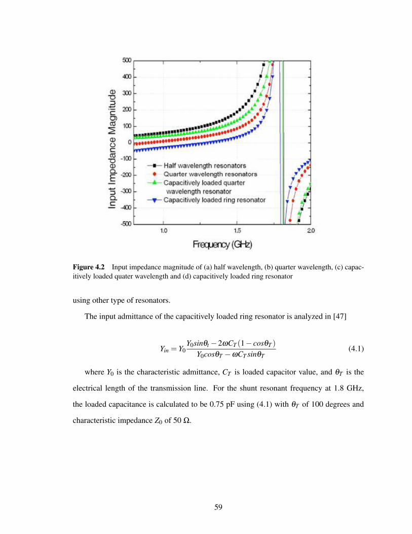
Figure 4.2 Input impedance magnitude of (a) half wavelength, (b) quarter wavelength, (c) capac-itively loaded quater wavelength and (d) capacitively loaded ring resonator
using other type of resonators.
The input admittance of the capacitively loaded ring resonator is analyzed in [47]
Yin = Y0Y0sinθt −2ωCT (1− cosθT )
Y0cosθT −ωCT sinθT(4.1)
where Y0 is the characteristic admittance, CT is loaded capacitor value, and θT is the
electrical length of the transmission line. For the shunt resonant frequency at 1.8 GHz,
the loaded capacitance is calculated to be 0.75 pF using (4.1) with θT of 100 degrees and
characteristic impedance Z0 of 50 Ω.
59

4.3 A Three Pole Bandpass Filter Design
A 3 pole bandpass filter with center frequency of 1.8 GHz and bandwidth of 6% is designed.
From (4.2) and (4.3) [48], the mutual coupling coefficient between the two adjacent res-
onators and the input/output external resonators’ Q are determined to be M1,2 = M2,3 =
0.055, Qe1 = Qe3 = 17.2.
Mi,i+1 =FBW√gigi+1
(4.2)
Qei =gi−1gi
FBW(4.3)
where FBW is the fractional bandwidth and gi is the element value for low pass pro-
totype. The full wave simulator IE3D [49] is used to determine the mutual coupling
coefficient and the external Qs by the method described in [48]. In order to perform on
wafer probe measurement, a micrsotrip line to CPW transition is adopted from [50]. The
filter layout is shown in Figure 4.3.
Figure 4.3 Layout of 3 pole tunable filter
The width of the ring transmission line is 347 µm with a characteristic impedance of
50 ohm. The spacing (S1) between adjacent resonators is 320 µm, and tapping point (L1)
60

for the input/output stage is 2120 µm. W1 is 2200 µm, W2 is 1070 µm, L2 is 6200 µm and
L3 is 4000 µm. The signal line width of the CPW line is 50 µm, and the gap size is 28 µm.
4.4 Filter Fabrication
A single side polished sapphire (Al2O3) with 430 µm thickness and dielectric constant of
11.58 is used as substrate. The BST varactor is implemented by two parallel plate ca-
pacitors connected in series. The bottom electrode, which is a metal stack of Ti/Au/Pt
(100/2000/1000 A), is evaporated and patterned by a standard lift-off process. Then BST
thin film is deposited by the pulsed layer deposition (PLD) technique using an excimer
laser (λ = 248 nm, 25 ns pulse width, 10 Hz, 200 mJ) with substrate temperature of 600
°C in 30 mTorr oxygen environment for 60 minutes. After this, the sample is annealed at
the same temperature in 100 Torr oxygen for 30 minutes to reduce oxygen vacancies in
the BST film. The BST thin film has a thickness of 250 nm. The top electrode of Pt/Au
(1000/2000 A) is completed in the same process as the bottom electrode. A high resistivity
material, SiCr, is deposited to form biasing lines for the varactors. SiCr thin film has a
thickness of 720 A and a sheet resistance of 800 ohm/sq. Each capacitively loaded ring res-
onator needs two bias lines, one of which is connected to the bottom electrode between two
parallel capacitors in series. By doing this, these BST capacitors act as loading capacitors
as well as DC blocking capacitors. The other line is connected to transmission line of the
resonator. Then filter trace is patterned to 8 µm gold which is 4 times thicker than the skin
depth at this frequency to reduce the metal loss. The fabricated filter is shown in Figure
4.4, and the inset shows the close view of BST varactor and SiCr biasing line. The total
circuit size is 14 mm by 22 mm.
61

Figure 4.4 Micro-graph of fabricated 3 pole tunable filter
4.5 Filter Measurement Results
The input and output of the filter are connected to two 150 µm GSG probes, and the filter is
measured by the Agilent E8364B VNA. On wafer through-reflection-line (TRL) calibration
kit is used to calibrate out the CPW to micrsotrip line transitions.
At zero bias, the center frequency of the filter is 2.05 GHz with an insertion loss of 6.4
dB. The return loss of the filter is better than 20 dB. The 3 dB bandwidth is found to be 8%,
as shown in Figure 4.5. The shift of the center frequency and bandwidth from the design
values may be due to the decrease of capacitance of the BST varactors.
On wafer testing BST varactors are measured, and the device performance is charac-
terized by the two port measurement technique described in chapter 2. The extracted loss
tangent is 0.021 over the desired frequency band, and the total device quality factor is 40.
The insertion loss is mainly due to varactor’s low quality factor. The insertion loss of the
filter is simulated to be 5.9 dB when BST varactors exhibit Q factor of 40. Another source
62

Figure 4.5 Measured filter response when no DC bias is applied.
of the loss is from the SiCr bias line fed to the BST varactors. The loss contributed by this
800 ohm/sq bias line is simulated to be approximate 0.5 dB. With a DC bias voltage from 0
to 10 volts, the center frequency is varied from 2.05 GHz to 2.41 GHz which corresponds
to a 20% tunability. The return loss is better than 10 dB over this frequency range, and the
insertion loss increases from 6.4 dB to 9.9 dB as shown in Figure 4.6. The 3 dB bandwidth
is nearly constant from 8% to 8.3% with 3.75% change.
4.6 Conclusion
A fully integrated 2 GHz 8% bandwidth tunable bandpass filter using BST varactor is de-
signed, fabricated and measured. Capacitively loaded ring resonators are used to design
this filter because they provide a easy way of frequency tuning and sharper filter out-of-
63

Figure 4.6 (a)Insertion loss and (b) return loss of the tunable microwave filter with DC bias volt-age from 0 V to 10 V.
64
band rejection. The measured insertion loss of the filter at zero bias voltage is 6.4 dB with
the BST varactor Q of 40. Under 10 volts bias, the filter can be tuned from 2.05 GHz to
2.41 GHz, giving a 20% center frequency tunability while the fractional bandwidth is kept
constant. The return loss is lower than 10 dB over the entire tuning frequency range. The
filter performance can be improved as the BST varactors’ Q-factors are increased.
65

Chapter 5
SWITCHABLE ACOUSTIC WAVE RESONATORS AND FILTERSUSING FERROELECTRIC THIN FILMS
5.1 Introduction
Multi-band and multi-mode wireless handsets are of great interest for the future wireless
communications. These devices require a switchable filter bank to select the frequency
band for each wireless standard. Switchable filter banks based on current filter technolo-
gies require external switches using solid state or MEMS devices. Incorporating external
switches in the path of RF signal results in increased loss, circuit complexity and cost.
In order to address these challenges, switchable acoustic wave resonators and filters us-
ing ferroelectric thin films are proposed here. Our aim is to use the electrostrictive or
DC electric field induced piezoelectric effect which was first studied in the bulk ferro-
electrics in the 1950’s [51, 52]. Recently these effects have been observed in thin film
ferroelectric materials [53, 54]. Acoustic wave resonators based on ferroelectric thin films
can be effectively switched on and off by the application of a DC bias voltage. There-
fore, no external switches are needed. Switchable filter banks using ferroelectric thin film
based acoustic wave resonators can achieve higher cicuit performance, smaller footprint
and lower cost. This chapter first discusses the electrostrictive effect in ferroelectric thin
films. Then FBARs using BST thin film are presented along with a modeling method, fabri-
cation process and the measurement results. Ladder type filters using ferroelectric thin film
acoustic wave resonators are designed and experimentally demonstrated. Finally contour
mode acoustic wave resonators using BTO thin films are studied, fabricated and measured.
66
5.2 Piezoelectricity and Electrostriction
Piezoelectricity was first discovered in 1880 by the Curie brothers. The piezoelectric ef-
fect desribes an electrical polarization induced by an mechanical stress in crystals. The
converse piezoelectric effect is defined as an applied electric field inducing a strain. This
relation is methematically defined as shown in (5.1) and (5.2).
S = sET +dT E (5.1)
D = dT + εT E (5.2)
where S is strain, s is compliance, T is stress, D is electric displacement, d is piezoelec-
tric coefficient, ε is permittivity, E is electric field strength; superscript E indicates a zero
or constant electric field, and superscript T a zero or constant stress field.
The piezoelectric effect shows a linear relation between mechanical and electrical do-
mains coupling, defined by piezoelectric coefficient d. There also exists a quadratic relation
due to the electrostrictive effect. A general relation between the induced strain (S) and the
electrical polarization (P) is describe in (5.3), assuming there’s no applied stress.
S = QP2 (5.3)
where Q is the electrostriction coefficient. With the applied electric field, the polariza-
tion is defined as (5.4)
P = Ps + χE (5.4)
where Ps is the spontaneous polarization, χ is the susceptibility and χE is the induced
67
polarization due to the applied electrical field E. From (5.3) and (5.4), one can obtain
S = QP2s +2QPsχE +Qχ2E2 (5.5)
The total strain consist of three parts: the spontaneous strain, the linear piezoelectric
strain, and the quadratic electrostrictive strain. Ferroelectric materials possess piezoelec-
tric effects due to the spontaneous polarization caused by the non-centrosymmetrical crystal
structure. The resultant piezoelectric effect shows hysteresis following the polarization hys-
teresis. In the paraelectric phase, there’s no piezoelectric effect since the crystal structure
is centrosymmetrical. Therefore, the electrostrictive effect dominates. Due to the electrical
field dependant polarization, the electrostrictive effects are dependant on the applied elec-
trical field. This unique property allows us to control the mechanical/electrical coupling by
the applied DC bias voltage. The converse piezoelectric/electrostrictive effect can be used
to generate acoustic waves. For piezoelectric material, the strength of the acoustic waves
can only be changed by the amplitude of the AC electrical signal. In the ferroelectric ma-
terials, the generation and strength of the acoustic waves are dependant on the applied DC
electric field.
A piezoelectric resonator is mainly made of a piezoelectric material such as quartz,
aluminum nitride (AlN) or zinc oxide (ZnO). When an alternating electric field at the
proper frequency is applied to the piezoelectric material, acoustic wave vibrations are ex-
cited through the direct and converse piezoelectric effects. The piezoelectric resonators can
be excited into different resonance modes such as thickness mode, shear mode or contour
mode, depending on which piezoelectric coefficient is used and the geometrical dimensions
determining the resonance frequency. Using ferroelectric materials instead of piezoelectric
materials, the acoustic wave resonance will be controlled by the DC bias voltage. Therefore
switchable acoustic wave resonators can be fabricated using ferroelectric materials.
68

Figure 5.1 BST FBAR structure
5.3 Thickness Mode Acoustic Wave Resonators Design
Thin film bulk acoustic wave resonators (FBARs) are thickness mode acoustic wave res-
onators. The resonance frequency is inversely proportional to the resonator thickness.
FBARs using ferroelectric thin films can be modeled in the same way as the FBARs using
piezoelectric thin films such as aluminum nitride (AlN) and zinc oxide (ZnO). An acoustic
wave transmission line model [55] is used to model FBARs using ferroelectric BST thin
films here.
The BST FBAR is composed of Si substrate, SiO2 buffer layer, bottom platinum
electrode, BST thin film, and the top platinum electrode as shown in Figure 5.1. The fun-
damental resonance frequency is mainly determined by the longitudinal acoustic velocity
in the BST thin film and its thickness as given by (5.6).
fn =vac
tBSTn, n = 1,2,3, ... (5.6)
where vac is the acoustic wave velocity in the BST thin film, and tBST is the thickness
69
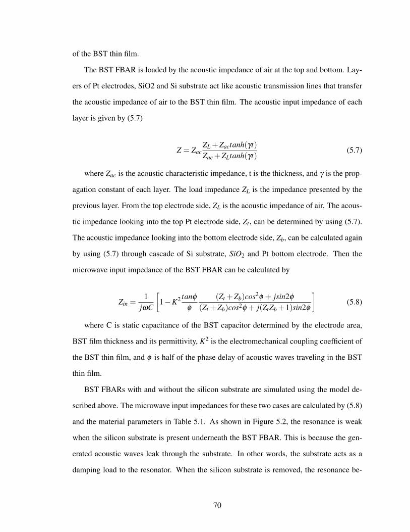
of the BST thin film.
The BST FBAR is loaded by the acoustic impedance of air at the top and bottom. Lay-
ers of Pt electrodes, SiO2 and Si substrate act like acoustic transmission lines that transfer
the acoustic impedance of air to the BST thin film. The acoustic input impedance of each
layer is given by (5.7)
Z = ZacZL +Zactanh(γt)Zac +ZLtanh(γt)
(5.7)
where Zac is the acoustic characteristic impedance, t is the thickness, and γ is the prop-
agation constant of each layer. The load impedance ZL is the impedance presented by the
previous layer. From the top electrode side, ZL is the acoustic impedance of air. The acous-
tic impedance looking into the top Pt electrode side, Zt , can be determined by using (5.7).
The acoustic impedance looking into the bottom electrode side, Zb, can be calculated again
by using (5.7) through cascade of Si substrate, SiO2 and Pt bottom electrode. Then the
microwave input impedance of the BST FBAR can be calculated by
Zin =1
jωC
[1−K2 tanφ
φ(Zt +Zb)cos2φ + jsin2φ
(Zt +Zb)cos2φ + j(ZtZb +1)sin2φ
](5.8)
where C is static capacitance of the BST capacitor determined by the electrode area,
BST film thickness and its permittivity, K2 is the electromechanical coupling coefficient of
the BST thin film, and φ is half of the phase delay of acoustic waves traveling in the BST
thin film.
BST FBARs with and without the silicon substrate are simulated using the model de-
scribed above. The microwave input impedances for these two cases are calculated by (5.8)
and the material parameters in Table 5.1. As shown in Figure 5.2, the resonance is weak
when the silicon substrate is present underneath the BST FBAR. This is because the gen-
erated acoustic waves leak through the substrate. In other words, the substrate acts as a
damping load to the resonator. When the silicon substrate is removed, the resonance be-
70
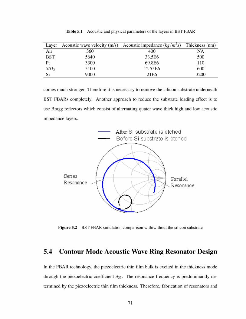
Table 5.1 Acoustic and physical parameters of the layers in BST FBAR
Layer Acoustic wave velocity (m/s) Acoustic impedance (kg/m2s) Thickness (nm)Air 360 400 NABST 5640 33.5E6 500Pt 3300 69.8E6 110SiO2 5100 12.55E6 600Si 9000 21E6 3200
comes much stronger. Therefore it is necessary to remove the silicon substrate underneath
BST FBARs completely. Another approach to reduce the substrate loading effect is to
use Bragg reflectors which consist of alternating quater wave thick high and low acoustic
impedance layers.
Figure 5.2 BST FBAR simulation comparison with/without the silicon substrate
5.4 Contour Mode Acoustic Wave Ring Resonator Design
In the FBAR technology, the piezoelectric thin film bulk is excited in the thickness mode
through the piezoelectric coefficient d33. The resonance frequency is predominantly de-
termined by the piezoelectric thin film thickness. Therefore, fabrication of resonators and
71
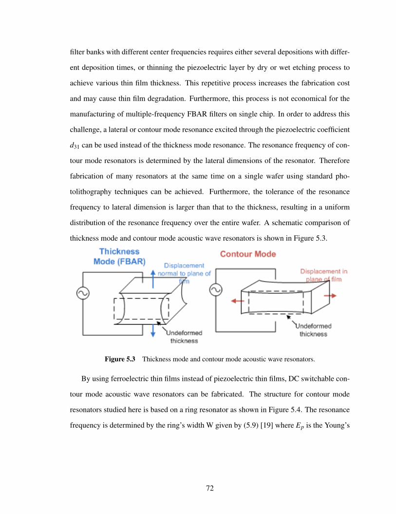
filter banks with different center frequencies requires either several depositions with differ-
ent deposition times, or thinning the piezoelectric layer by dry or wet etching process to
achieve various thin film thickness. This repetitive process increases the fabrication cost
and may cause thin film degradation. Furthermore, this process is not economical for the
manufacturing of multiple-frequency FBAR filters on single chip. In order to address this
challenge, a lateral or contour mode resonance excited through the piezoelectric coefficient
d31 can be used instead of the thickness mode resonance. The resonance frequency of con-
tour mode resonators is determined by the lateral dimensions of the resonator. Therefore
fabrication of many resonators at the same time on a single wafer using standard pho-
tolithography techniques can be achieved. Furthermore, the tolerance of the resonance
frequency to lateral dimension is larger than that to the thickness, resulting in a uniform
distribution of the resonance frequency over the entire wafer. A schematic comparison of
thickness mode and contour mode acoustic wave resonators is shown in Figure 5.3.
Figure 5.3 Thickness mode and contour mode acoustic wave resonators.
By using ferroelectric thin films instead of piezoelectric thin films, DC switchable con-
tour mode acoustic wave resonators can be fabricated. The structure for contour mode
resonators studied here is based on a ring resonator as shown in Figure 5.4. The resonance
frequency is determined by the ring’s width W given by (5.9) [19] where Ep is the Young’s
72
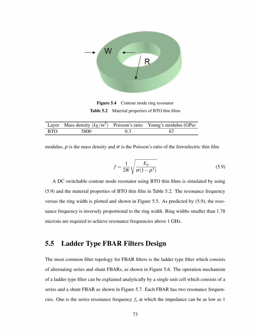
Figure 5.4 Contour mode ring resonator
Table 5.2 Material properties of BTO thin films
Layer Mass density (kg/m3) Poisson’s ratio Young’s modulus (GPa)BTO 5800 0.3 67
modulus, ρ is the mass density and σ is the Poisson’s ratio of the ferroelectric thin film
f =1
2W
√Ep
σ(1−ρ2)(5.9)
A DC switchable contour mode resonator using BTO thin films is simulated by using
(5.9) and the material properties of BTO thin film in Table 5.2. The resonance frequency
versus the ring width is plotted and shown in Figure 5.5. As predicted by (5.9), the reso-
nance frequency is inversely proportional to the ring width. Ring widths smaller than 1.78
microns are required to achieve resonance frequencies above 1 GHz.
5.5 Ladder Type FBAR Filters Design
The most common filter topology for FBAR filters is the ladder type filter which consists
of alternating series and shunt FBARs, as shown in Figure 5.6. The operation mechanism
of a ladder type filter can be explained analytically by a single unit cell which consists of a
series and a shunt FBAR as shown in Figure 5.7. Each FBAR has two resonance frequen-
cies. One is the series resonance frequency fs at which the impedance can be as low as 1
73
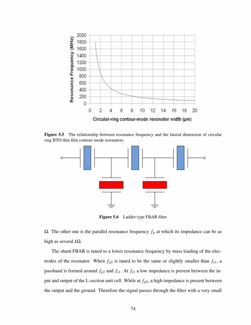
Figure 5.5 The relationship between resonance frequency and the lateral dimension of circularring BTO thin film contour mode resonators.
Figure 5.6 Ladder type FBAR filter
Ω. The other one is the parallel resonance frequency fp at which its impedance can be as
high as several kΩ.
The shunt FBAR is tuned to a lower resonance frequency by mass loading of the elec-
trodes of the resonator. When fp2 is tuned to be the same or slightly smaller than fs1, a
passband is formed around fp2 and fs1. At fs1 a low impedance is present between the in-
put and output of the L-section unit cell. While at fp2, a high impedance is present between
the output and the ground. Therefore the signal passes through the filter with a very small
74
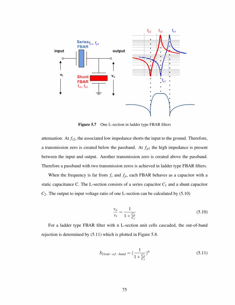
Figure 5.7 One L-section in ladder type FBAR filters
attenuation. At fs2, the associated low impedance shorts the input to the ground. Therefore,
a transmission zero is created below the passband. At fp1 the high impedance is present
between the input and output. Another transmission zero is created above the passband.
Therefore a passband with two transmission zeros is achieved in ladder type FBAR filters.
When the frequency is far from fs and fp, each FBAR behaves as a capacitor with a
static capacitance C. The L-section consists of a series capacitor C1 and a shunt capacitor
C2. The output to input voltage ratio of one L-section can be calculated by (5.10)
vo
vi=
1
1+ C2C1
(5.10)
For a ladder type FBAR filter with n L-section unit cells cascaded, the out-of-band
rejection is determined by (5.11) which is plotted in Figure 5.8.
S21out−o f−band = (1
1+ C2C1
)n (5.11)
75
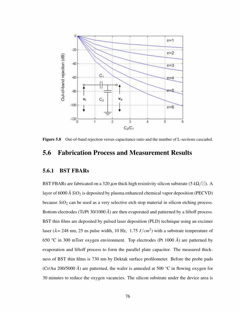
Figure 5.8 Out-of-band rejection versus capacitance ratio and the number of L-sections cascaded.
5.6 Fabrication Process and Measurement Results
5.6.1 BST FBARs
BST FBARs are fabricated on a 320 µm thick high resistivity silicon substrate (5 kΩ/¡). A
layer of 6000 A SiO2 is deposited by plasma enhanced chemical vapor deposition (PECVD)
because SiO2 can be used as a very selective etch stop material in silicon etching process.
Bottom electrodes (Ti/Pt 30/1000 A) are then evaporated and patterned by a liftoff process.
BST thin films are deposited by pulsed laser deposition (PLD) technique using an excimer
laser (λ= 248 nm, 25 ns pulse width, 10 Hz, 1.75 J/cm2) with a substrate temperature of
650 °C in 300 mTorr oxygen environment. Top electrodes (Pt 1000 A) are patterned by
evaporation and liftoff process to form the parallel plate capacitor. The measured thick-
ness of BST thin films is 730 nm by Dektak surface profilometer. Before the probe pads
(Cr/Au 200/5000 A) are patterned, the wafer is annealed at 500 °C in flowing oxygen for
30 minutes to reduce the oxygen vacancies. The silicon substrate under the device area is
76
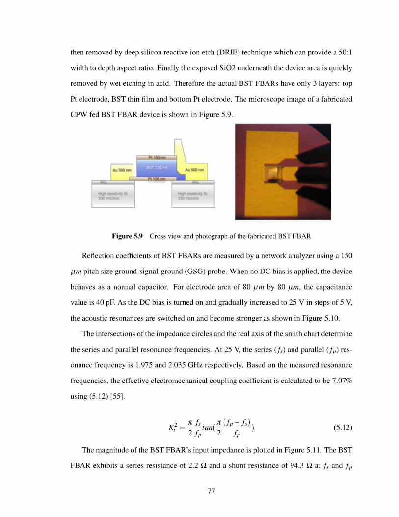
then removed by deep silicon reactive ion etch (DRIE) technique which can provide a 50:1
width to depth aspect ratio. Finally the exposed SiO2 underneath the device area is quickly
removed by wet etching in acid. Therefore the actual BST FBARs have only 3 layers: top
Pt electrode, BST thin film and bottom Pt electrode. The microscope image of a fabricated
CPW fed BST FBAR device is shown in Figure 5.9.
Figure 5.9 Cross view and photograph of the fabricated BST FBAR
Reflection coefficients of BST FBARs are measured by a network analyzer using a 150
µm pitch size ground-signal-ground (GSG) probe. When no DC bias is applied, the device
behaves as a normal capacitor. For electrode area of 80 µm by 80 µm, the capacitance
value is 40 pF. As the DC bias is turned on and gradually increased to 25 V in steps of 5 V,
the acoustic resonances are switched on and become stronger as shown in Figure 5.10.
The intersections of the impedance circles and the real axis of the smith chart determine
the series and parallel resonance frequencies. At 25 V, the series ( fs) and parallel ( fp) res-
onance frequency is 1.975 and 2.035 GHz respectively. Based on the measured resonance
frequencies, the effective electromechanical coupling coefficient is calculated to be 7.07%
using (5.12) [55].
K2t =
π2
fs
fptan(
π2
( fp− fs)fp
) (5.12)
The magnitude of the BST FBAR’s input impedance is plotted in Figure 5.11. The BST
FBAR exhibits a series resistance of 2.2 Ω and a shunt resistance of 94.3 Ω at fs and fp
77
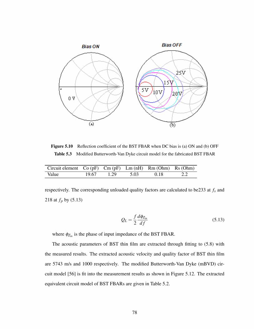
Figure 5.10 Reflection coefficient of the BST FBAR when DC bias is (a) ON and (b) OFF
Table 5.3 Modified Butterworth-Van Dyke circuit model for the fabricated BST FBAR
Circuit element Co (pF) Cm (pF) Lm (nH) Rm (Ohm) Rs (Ohm)Value 19.67 1.29 5.03 0.18 2.2
respectively. The corresponding unloaded quality factors are calculated to be233 at fs and
218 at fp by (5.13)
QL =f2
dφZin
d f(5.13)
where φZin is the phase of input impedance of the BST FBAR.
The acoustic parameters of BST thin film are extracted through fitting to (5.8) with
the measured results. The extracted acoustic velocity and quality factor of BST thin film
are 5743 m/s and 1000 respectively. The modified Butterworth-Van Dyke (mBVD) cir-
cuit model [56] is fit into the measurement results as shown in Figure 5.12. The extracted
equivalent circuit model of BST FBARs are given in Table 5.2.
78

Figure 5.11 Magnitude of the input impedance of the BST FBAR
5.6.2 A 1.5 Stage Ladder Type BTO FBAR Filter
A switchable 1.5 stage ladder FBAR filter has been designed and fabricated. The filter
consists of two series resonators and two shunt resonators as shown in Figure 5.13. Each
resonator is made of a BTO thin film sandwiched between two platinum electrodes. The
total capacitance of the shunt resonators is chosen to be four times the capacitance of the
series resonator in order to achieve a better out-of-band rejection. The symmetric place-
ment of the shunt resonators allows for on wafer measurement using coplanar probes. The
four BTO FBARs within the filter must be biased at the same voltage level for proper filter
operation. This is accomplished by applying the bias voltage to the bottom electrode which
is shared by the four resonators. The top electrodes are connected to DC ground. A high
resistivity material SiCr is used for the DC bias line.
The BTO switchable FBAR filter is fabricated on a high resistivity silicon substrate (5
kΩcm) with a thickness of 525 µm. A 1 µm thermal oxide buffer layer is deposited on
top of the substrate. A 100 nm bottom electrode of platinum is patterned by e-beam evap-
79
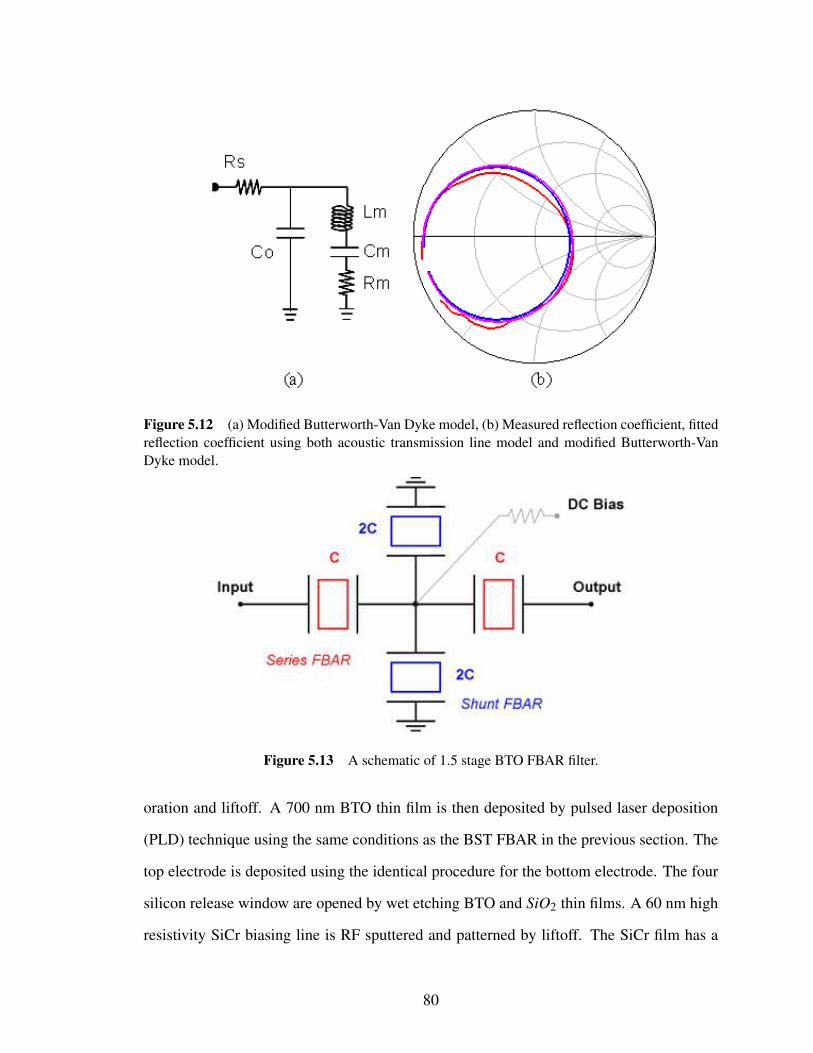
Figure 5.12 (a) Modified Butterworth-Van Dyke model, (b) Measured reflection coefficient, fittedreflection coefficient using both acoustic transmission line model and modified Butterworth-VanDyke model.
Figure 5.13 A schematic of 1.5 stage BTO FBAR filter.
oration and liftoff. A 700 nm BTO thin film is then deposited by pulsed laser deposition
(PLD) technique using the same conditions as the BST FBAR in the previous section. The
top electrode is deposited using the identical procedure for the bottom electrode. The four
silicon release window are opened by wet etching BTO and SiO2 thin films. A 60 nm high
resistivity SiCr biasing line is RF sputtered and patterned by liftoff. The SiCr film has a
80
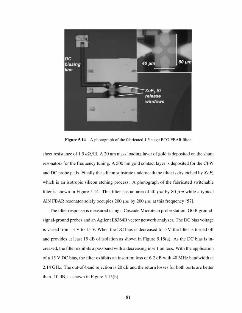
Figure 5.14 A photograph of the fabricated 1.5 stage BTO FBAR filter.
sheet resistance of 1.5 kΩ/¡. A 20 nm mass loading layer of gold is deposited on the shunt
resonators for the frequency tuning. A 500 nm gold contact layer is deposited for the CPW
and DC probe pads. Finally the silicon substrate underneath the filter is dry etched by XeF2
which is an isotropic silicon etching process. A photograph of the fabricated switchable
filter is shown in Figure 5.14. This filter has an area of 40 µm by 80 µm while a typical
AlN FBAR resonator solely occupies 200 µm by 200 µm at this frequency [57].
The filter response is measured using a Cascade Microtech probe station, GGB ground-
signal-ground probes and an Agilent E8364B vector network analyzer. The DC bias voltage
is varied from -3 V to 15 V. When the DC bias is decreased to -3V, the filter is turned off
and provides at least 15 dB of isolation as shown in Figure 5.15(a). As the DC bias is in-
creased, the filter exhibits a passband with a decreasing insertion loss. With the application
of a 15 V DC bias, the filter exhibits an insertion loss of 6.2 dB with 40 MHz bandwidth at
2.14 GHz. The out-of-band rejection is 20 dB and the return losses for both ports are better
than -10 dB, as shown in Figure 5.15(b).
81
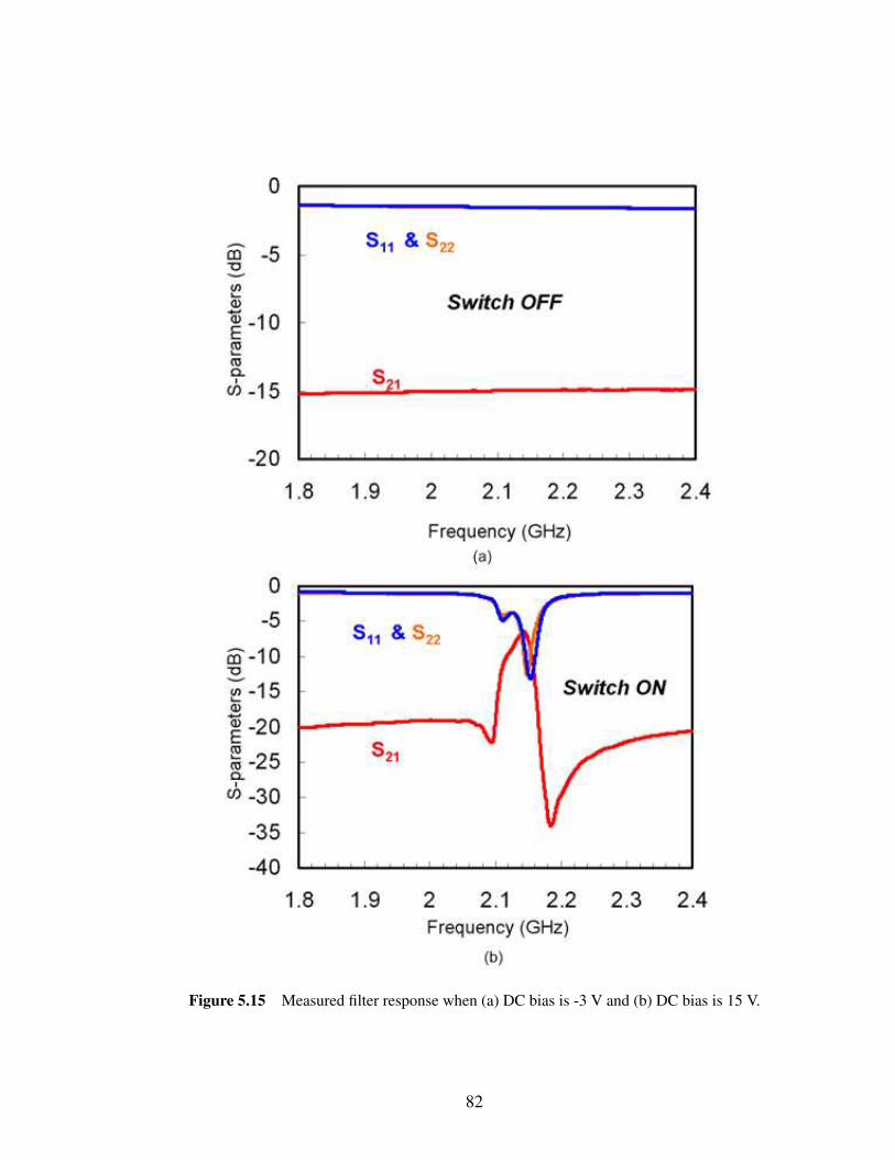
Figure 5.15 Measured filter response when (a) DC bias is -3 V and (b) DC bias is 15 V.
82

Figure 5.16 Comparison of measured and simulated filter response.
Both the series and the shunt resonators in the switchable filter are measured. The se-
ries resonators have a series resonance frequency of 2.14 GHz and an associated Q-factor
of 97. The shunt resonators have a de-tuned series resonance frequency of 2.09 GHz and
an associated Q-factor of 64. The electromechanical coupling coefficient is measured to be
4.2% for the series resonators and 4.9% for the shunt resonators. The static capacitance is
measured to be 0.65 pF for the series resonators and 1.5 pF for the shunt resonators. Both
the series and shunt resonators are modeled using the Butterworth-Van Dyke (BVD) cir-
cuit model. These models are used for the filter simulation. The simulated filter response
matches well with the measurement results as shown in Figure 5.16. The large insertion
loss is mainly due to the low Q-factor of the BTO FBARs. As the Q-factor is increase
to 1000 which is a typical value for AlN FBARs [58], the insertion loss is improved to 2
dB in the simulation, as shown in Figure 5.16. Therefore, material study and optimization
of ferroelectric thin films are necessary to achieve higher quality factors and better filter
performance.
83
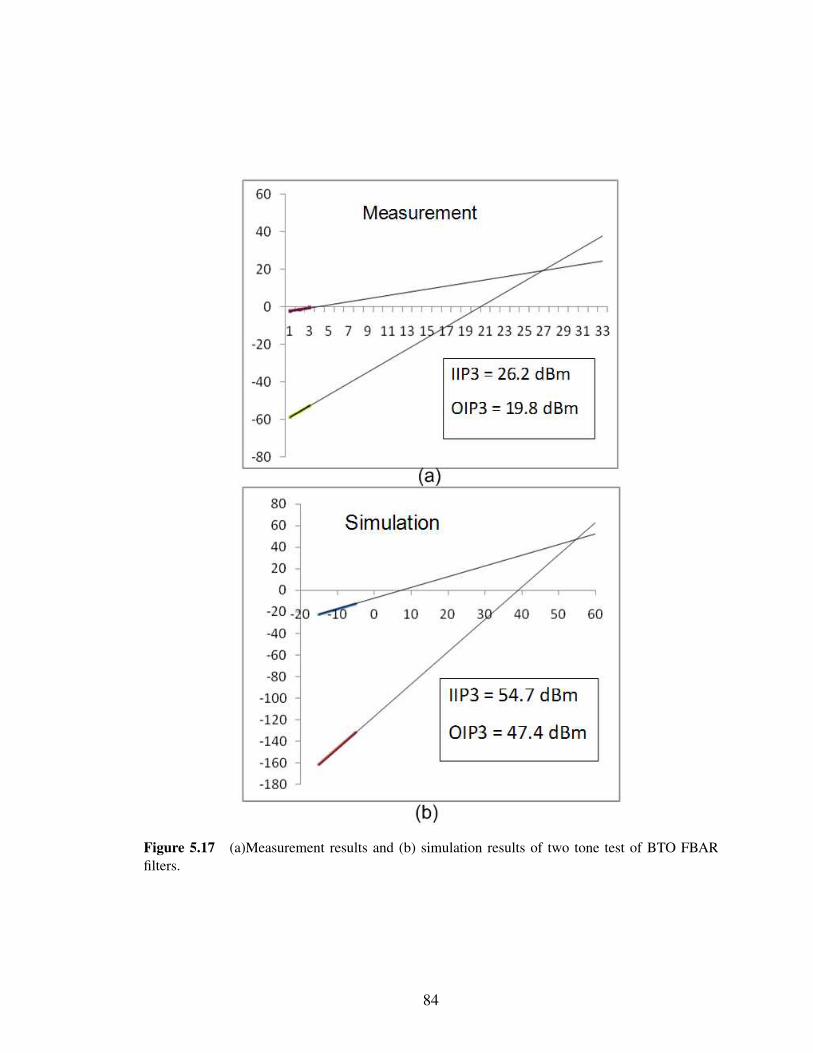
Figure 5.17 (a)Measurement results and (b) simulation results of two tone test of BTO FBARfilters.
84
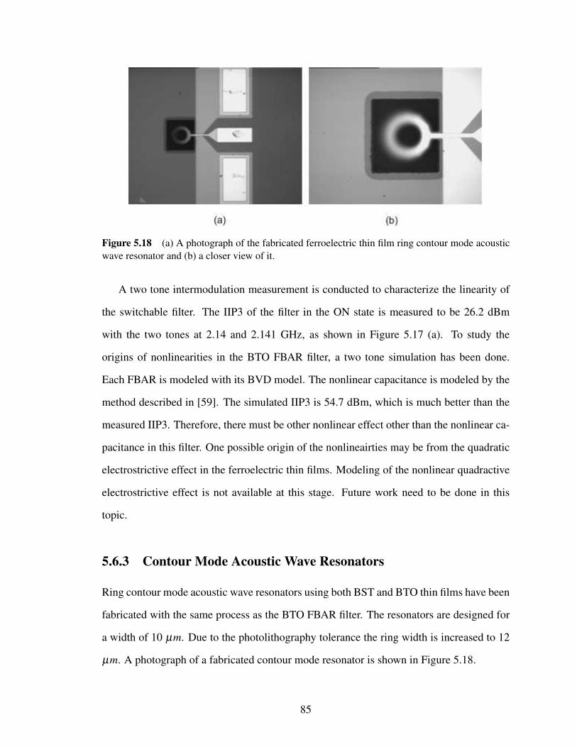
Figure 5.18 (a) A photograph of the fabricated ferroelectric thin film ring contour mode acousticwave resonator and (b) a closer view of it.
A two tone intermodulation measurement is conducted to characterize the linearity of
the switchable filter. The IIP3 of the filter in the ON state is measured to be 26.2 dBm
with the two tones at 2.14 and 2.141 GHz, as shown in Figure 5.17 (a). To study the
origins of nonlinearities in the BTO FBAR filter, a two tone simulation has been done.
Each FBAR is modeled with its BVD model. The nonlinear capacitance is modeled by the
method described in [59]. The simulated IIP3 is 54.7 dBm, which is much better than the
measured IIP3. Therefore, there must be other nonlinear effect other than the nonlinear ca-
pacitance in this filter. One possible origin of the nonlineairties may be from the quadratic
electrostrictive effect in the ferroelectric thin films. Modeling of the nonlinear quadractive
electrostrictive effect is not available at this stage. Future work need to be done in this
topic.
5.6.3 Contour Mode Acoustic Wave Resonators
Ring contour mode acoustic wave resonators using both BST and BTO thin films have been
fabricated with the same process as the BTO FBAR filter. The resonators are designed for
a width of 10 µm. Due to the photolithography tolerance the ring width is increased to 12
µm. A photograph of a fabricated contour mode resonator is shown in Figure 5.18.
85
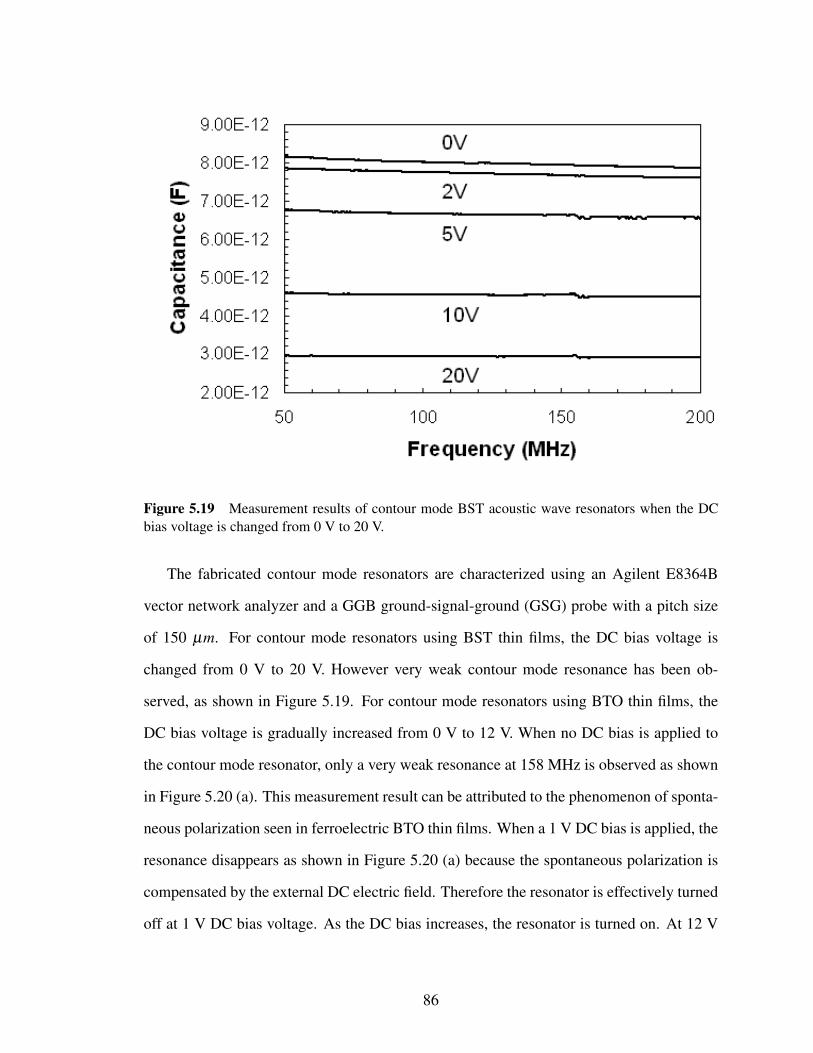
Figure 5.19 Measurement results of contour mode BST acoustic wave resonators when the DCbias voltage is changed from 0 V to 20 V.
The fabricated contour mode resonators are characterized using an Agilent E8364B
vector network analyzer and a GGB ground-signal-ground (GSG) probe with a pitch size
of 150 µm. For contour mode resonators using BST thin films, the DC bias voltage is
changed from 0 V to 20 V. However very weak contour mode resonance has been ob-
served, as shown in Figure 5.19. For contour mode resonators using BTO thin films, the
DC bias voltage is gradually increased from 0 V to 12 V. When no DC bias is applied to
the contour mode resonator, only a very weak resonance at 158 MHz is observed as shown
in Figure 5.20 (a). This measurement result can be attributed to the phenomenon of sponta-
neous polarization seen in ferroelectric BTO thin films. When a 1 V DC bias is applied, the
resonance disappears as shown in Figure 5.20 (a) because the spontaneous polarization is
compensated by the external DC electric field. Therefore the resonator is effectively turned
off at 1 V DC bias voltage. As the DC bias increases, the resonator is turned on. At 12 V
86
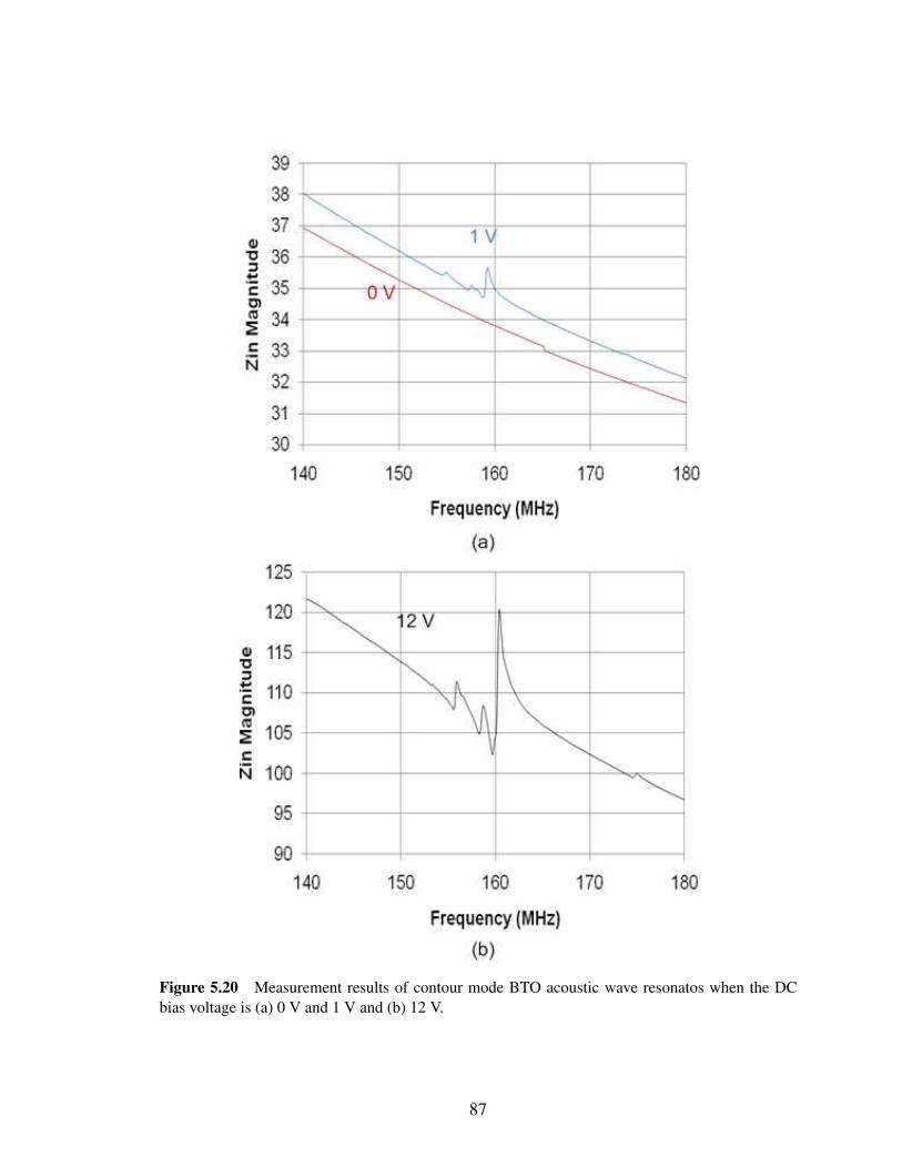
Figure 5.20 Measurement results of contour mode BTO acoustic wave resonatos when the DCbias voltage is (a) 0 V and 1 V and (b) 12 V.
87
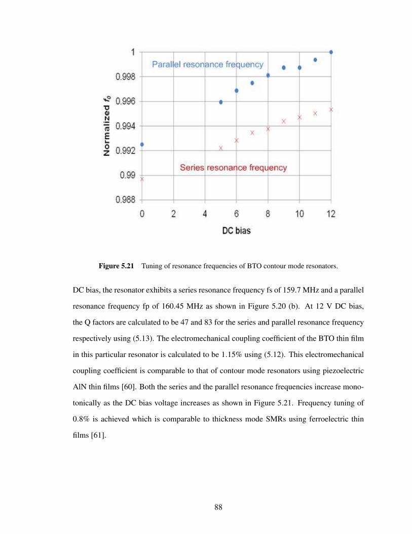
Figure 5.21 Tuning of resonance frequencies of BTO contour mode resonators.
DC bias, the resonator exhibits a series resonance frequency fs of 159.7 MHz and a parallel
resonance frequency fp of 160.45 MHz as shown in Figure 5.20 (b). At 12 V DC bias,
the Q factors are calculated to be 47 and 83 for the series and parallel resonance frequency
respectively using (5.13). The electromechanical coupling coefficient of the BTO thin film
in this particular resonator is calculated to be 1.15% using (5.12). This electromechanical
coupling coefficient is comparable to that of contour mode resonators using piezoelectric
AlN thin films [60]. Both the series and the parallel resonance frequencies increase mono-
tonically as the DC bias voltage increases as shown in Figure 5.21. Frequency tuning of
0.8% is achieved which is comparable to thickness mode SMRs using ferroelectric thin
films [61].
88

5.7 Conclusion
Switchable acoustic wave resonators and filters have been demonstrated using ferroelectric
thin films. They is based on the electrostrictive or electric field induced piezoelectric effect
in ferroelectric thin films. Both thickness and contour mode resonators have been presented
with the intrinsic switching property by the DC bias voltage. A 1.5 stage ladder type BTO
FBAR filter has been designed, fabricated and measured with moderate insertion loss.
89
Chapter 6
CONCLUSIONS AND FUTURE WORK
6.1 Conclusions
Within this dissertation demonstration of switchable and tunable radio frequency com-
ponents using ferroelectric thin films are presented for the first time. These devices are
useful for reconfigurable wireless communication systems such as multi-band and multi-
mode wireless mobile phones and cognitive radios. This work includes ferroelectric thin
film deposition optimization, clean room fabrication process, BST varactors modeling and
measurement techniques, a tunable microwave filter using BST varactors, and switchable
acoustic wave resonators and filters based on ferroelectric thin films.
The presented two port measurement technique demonstrates both easier implemen-
tation and better accuracy than the commonly used one port reflection type measurement
technique. The uncertainty analysis of both techniques shows that two port measurement
technique is 30% less sensitive to the measurement errors than the one port measurement
technique. This technique can be useful for material scientist and engineers to characterize
the ferroelectric thin film in a confident way.
The PLD process is used to deposit ferroelectric thin films. By varying the deposition
conditions, an optimized PLD process can yield BST thin films with low loss tangents and
high tunabilities. Loss tangents of 0.01 has been achieved at lower GHz range for BST thin
films. A full clean room fabrication process has been developed for fabrication of tunable
microwave capacitors and circuits using BST thin films. Various fabricated varactors and
tunable circuits have been demonstrated.
90

A fully integrated 2 GHz 3 pole tunable bandpass filter using BST varactors has been
demonstrated. Capacitively loaded ring resonators are used in this filter to provide an easy
tuning and a good out-of-band rejection. The fabricated filter exhibits a 20% frequency
tunability with a moderate insertion loss.
Electrostrictive and electric field induced piezoelectric effects in the ferroelectric thin
films have been studied to realize intrinsically switchable acoustic wave resonators and
filters. Both thickness mode and contour mode switchable acoustic wave resonators have
been successfully demonstrated. At a DC bias of 25 V, BST FBARs exhibit Q-factors ex-
ceeding 200 at 2 GHz, and a large electromechanical coupling coefficient of 7%. Contour
mode resonance using BTO thin films are demonstrated at 150 MHz. A 1.5 stage ladder
type BTO FBAR filter is designed, fabricated and measured. At a DC bias of -3 V, the
filter is turned off. At a DC bias of 15 V, the filter is turned on. At the ON state, this filter
exhibits 40 MHz bandwidth passband at 2.14 GHz with an insertion loss of 6.2 dB. The
out-of-band rejection is better than 15 dB. This filter has a very compact size of 40 µm
by 80 µm. This is much smaller than piezoelectric AlN FBAR filters. Therefore one can
envision a switchable filter array in a very small footprint.
The demonstrated switchable and tunable RF components prove the ferroelectric thin
film technology as a good candidate for future wireless communication systems. The next
section will outline some ideas for the future work to improve and expand this technology.
6.2 Future Work
6.2.1 Low Temperature Deposition of Ferroelectric Thin Films UsingAtomic Layer Deposition
All the current deposition techniques for ferroelectric thin films require a very high temper-
ature exceeding 500 °C in order to achieve good crystalline films. However this prevents
the integration of ferroelectric thin films to the modern IC process in which the highest
91

tolerable process temperature is 400 °C. Atomic layer deposition (ALD) may provide a so-
lution for low temperature deposition of ferroelectric thin films due to the strong chemical
reaction among the precursor materials. ALD also have a number of merits such as, fine
film thickness control, very good 3D conformal coating, very few defects and etc. Several
groups have successfully demonstrated depositions of STO and BTO thin films using ALD
in the temperature range of 200 - 350 °C [62, 63]. Films with permittivity exceeding 100
have been achieved. In [62] Vehkamaki found that large oxidant water dose can improve
the film crystallinity without high temperature post process annealing. Recently an Oxford
OpAL ALD system was installed in the clean room at the University of Michigan. This can
help to initiate studies of ferroelectric thin films deposited by ALD at low temperatures.
6.2.2 Higher Frequency Switchable Contour Mode Resonators UsingFerroelectric Thin Films
The demonstrated contour mode resonator operates at 150 MHz. In order to operate at
higher frequencies such as in the GHz range, the ring width is calculated to be less than 1
µm. A single ring with such narrow width will be mechanically vulnerable, thus pose yield
problem. Instead, interdigitized contour mode resonators have been proposed for piezo-
electric AlN thin films [64]. The interdigital structure not only helps on the mechanical
toughness but also lowers the motional resistance which improves the impedance match-
ing. Therefore, high frequency interdigitized contour mode resonators using ferroelectric
thin films can be investigated. To realize small features such as sub-micron features, two
major fabrication issues need to be solved. The first issue is the alignment of sub-micron
features. This can be done by using a stepper aligner. The second issue is the etching of
ferroelectric thin films. Wet etching method using diluted HF is currently used to etch fer-
roelectric thin films. The etching speed is about 15 nm/sec which is too fast for sub-micron
features. Also it is experimentally found that the wet etching causes problems around the
edges of devices. To solve this problem, dry etching method can be used. Several work
92

on dry etching of ferroelectric thin films have been reported [65, 66] with a moderate etch
speed.
6.2.3 High Performance Switchable FBAR Filters Using FerroelectricThin Films
A BTO FBAR filter have been demonstrated with moderate insertion loss and out-of-band
rejection. Also cascading more sections of FBARs, a better out-of-band rejection can be
achieved at the expense of insertion loss. To lower the insertion loss, BTO FBARs need
to have higher Q-factors. In the future, studies of the material optimization for high Q-
factor should be carried out. One needs to understand the relation between the mechanical
Q-factor of ferroelectric thin films and the deposition conditions.
93

Appendices
94

Appendix A
Ferroelectric Thin Film Based Tunable Capacitors and CircuitsFabrication Process
A.1 Starting wafer: Sapphire, single-side polished, C-plane, 430 µm.
• Dice and blow dry using N2 gas.
• Soak in hot Xylene for 30 min.
• Rinse in the DI water for 5 min.
• N2 blow dry.
• Dehydration bake 130 °C for 3 min.
A.2 Bottom electrode evaporation and liftoff.
• Apply HMDS to substrate and let it stay for 30 sec.
• Spin HMDS at 4000 rpm for 30 sec.
• Spin 1813 at 4000 rpm for 30 sec.
• Soft bake at 105 °C for 1 min.
• Soak in chlorobenzen (CBZ) for 5 min.
• Image exposure 10 sec at 20 mW/cm2.
• Develop in MF319 for 1 min.
• Rinse in DI water for 3 min and N2 blow dry.
• Check the pattern under microscope.
• Oxygen asher at 250mT and 80W for 60 sec.
95
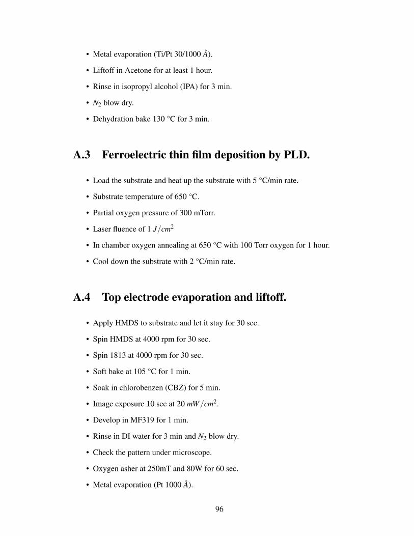
• Metal evaporation (Ti/Pt 30/1000 A).
• Liftoff in Acetone for at least 1 hour.
• Rinse in isopropyl alcohol (IPA) for 3 min.
• N2 blow dry.
• Dehydration bake 130 °C for 3 min.
A.3 Ferroelectric thin film deposition by PLD.
• Load the substrate and heat up the substrate with 5 °C/min rate.
• Substrate temperature of 650 °C.
• Partial oxygen pressure of 300 mTorr.
• Laser fluence of 1 J/cm2
• In chamber oxygen annealing at 650 °C with 100 Torr oxygen for 1 hour.
• Cool down the substrate with 2 °C/min rate.
A.4 Top electrode evaporation and liftoff.
• Apply HMDS to substrate and let it stay for 30 sec.
• Spin HMDS at 4000 rpm for 30 sec.
• Spin 1813 at 4000 rpm for 30 sec.
• Soft bake at 105 °C for 1 min.
• Soak in chlorobenzen (CBZ) for 5 min.
• Image exposure 10 sec at 20 mW/cm2.
• Develop in MF319 for 1 min.
• Rinse in DI water for 3 min and N2 blow dry.
• Check the pattern under microscope.
• Oxygen asher at 250mT and 80W for 60 sec.
• Metal evaporation (Pt 1000 A).
96

• Liftoff in Acetone for at least 1 hour.
• Rinse in isopropyl alcohol (IPA) for 3 min.
• N2 blow dry.
• Dehydration bake 130 °C for 3 min.
A.5 High temperature oxygen annealing.
• Furnace temperature at 500 °C.
• Flow oxygen with 2 sccm rate.
• Anneal for 30 min.
A.6 Ferroelectric thin film wet etch.
• Apply HMDS to substrate and let it stay for 30 sec.
• Spin HMDS at 4000 rpm for 30 sec.
• Spin 1827 at 4000 rpm for 30 sec.
• Soft bake at 105 °C for 1 min.
• Image exposure 10 sec at 20 mW/cm2.
• Develop in MF319 for 1 min.
• Rinse in DI water for 3 min and N2 blow dry.
• Check the pattern under microscope.
• Oxygen asher at 250mT and 80W for 60 sec.
• Hard bake 110 °C for 1 min.
• Wet etch in HF:DI (1:10) solution. (etch rate is about 200 nm for 20 sec)
• Rinse in DI water for 3 min and N2 blow dry.
• Inspect the film thickness by Dektak.
• Strip photoresist in aceton for at least 1 hour.
• Rinse in isopropyl alcohol (IPA) for 3 min.
97

• N2 blow dry.
• Dehydration bake 130 °C for 3 min.
A.7 Bias networks sputter and liftoff.
• Apply HMDS to substrate and let it stay for 30 sec.
• Spin HMDS at 4000 rpm for 30 sec.
• Spin 1827 at 4000 rpm for 30 sec.
• Soft bake at 105 °C for 1 min.
• Soak in chlorobenzen (CBZ) for 5 min.
• Image exposure 10 sec at 20 mW/cm2.
• Develop in MF319 for 1 min.
• Rinse in DI water for 3 min and N2 blow dry.
• Check the pattern under microscope.
• Oxygen asher at 250mT and 80W for 60 sec.
• RF sputter (SiCr 700 A).
• Liftoff in Acetone for at least 1 hour.
• Rinse in isopropyl alcohol (IPA) for 3 min.
• N2 blow dry.
• Dehydration bake 130 °C for 3 min.
A.8 Contact metal evaporation and liftoff.
• Apply HMDS to substrate and let it stay for 30 sec.
• Spin HMDS at 4000 rpm for 30 sec.
• Spin 1827 at 4000 rpm for 30 sec.
• Soft bake at 105 °C for 1 min.
• Soak in chlorobenzen (CBZ) for 5 min.
98

• Image exposure 10 sec at 20 mW/cm2.
• Develop in MF319 for 1 min.
• Rinse in DI water for 3 min and N2 blow dry.
• Check the pattern under microscope.
• Oxygen asher at 250mT and 80W for 60 sec.
• Metal evaporation (Ti/Au 500/5000 A).
• Liftoff in Acetone for at least 1 hour.
• Rinse in isopropyl alcohol (IPA) for 3 min.
• N2 blow dry.
• Dehydration bake 130 °C for 3 min.
A.9 Passivation layer deposition by PECVD.
• High temp SiO2 or SiN deposition (380 °C).
• Every time deposit 1000 A.
• Target thickness 5000-7000 A.
A.10 Passivation layer wet etch.
• Apply HMDS to substrate and let it stay for 30 sec.
• Spin HMDS at 4000 rpm for 30 sec.
• Spin 1827 at 4000 rpm for 30 sec.
• Soft bake at 105 °C for 1 min.
• Image exposure 10 sec at 20 mW/cm2.
• Develop in MF319 for 1 min.
• Rinse in DI water for 3 min and N2 blow dry.
• Check the pattern under microscope.
• Oxygen asher at 250mT and 80W for 60 sec.
99
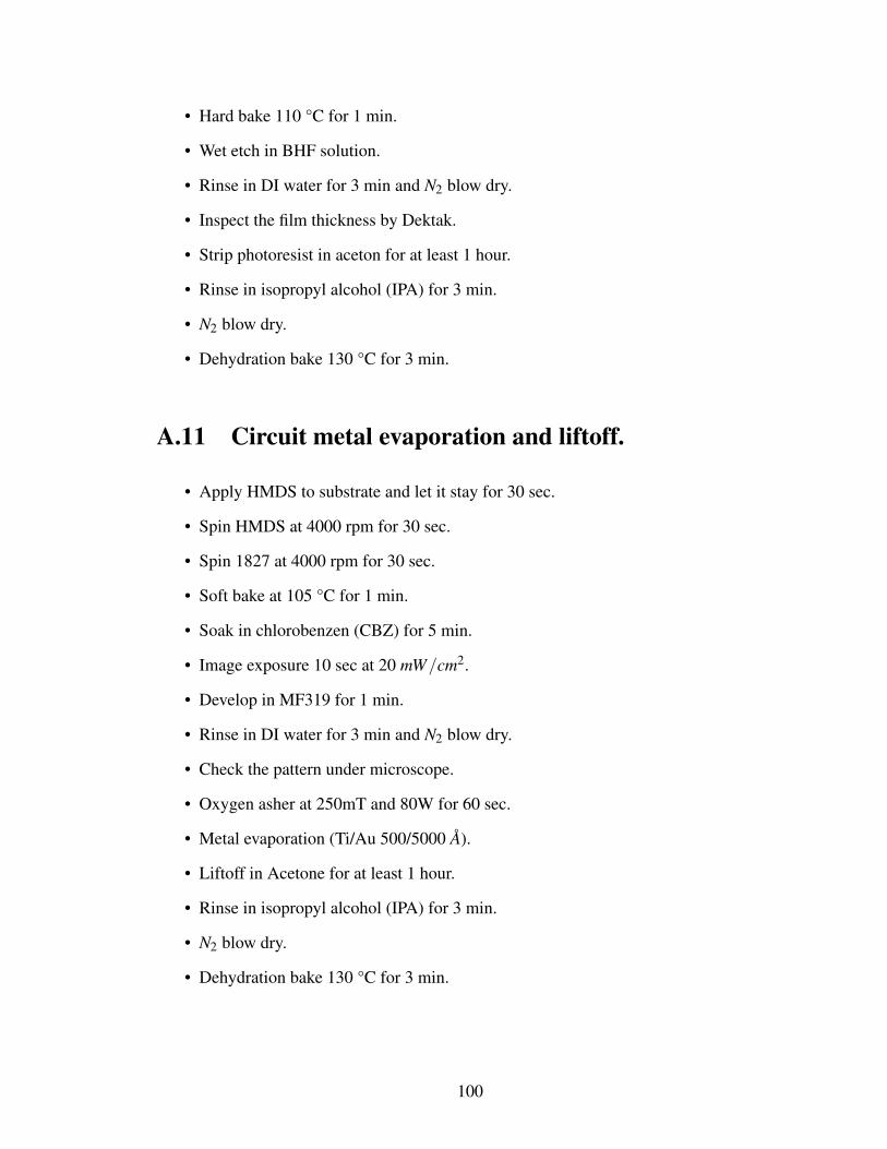
• Hard bake 110 °C for 1 min.
• Wet etch in BHF solution.
• Rinse in DI water for 3 min and N2 blow dry.
• Inspect the film thickness by Dektak.
• Strip photoresist in aceton for at least 1 hour.
• Rinse in isopropyl alcohol (IPA) for 3 min.
• N2 blow dry.
• Dehydration bake 130 °C for 3 min.
A.11 Circuit metal evaporation and liftoff.
• Apply HMDS to substrate and let it stay for 30 sec.
• Spin HMDS at 4000 rpm for 30 sec.
• Spin 1827 at 4000 rpm for 30 sec.
• Soft bake at 105 °C for 1 min.
• Soak in chlorobenzen (CBZ) for 5 min.
• Image exposure 10 sec at 20 mW/cm2.
• Develop in MF319 for 1 min.
• Rinse in DI water for 3 min and N2 blow dry.
• Check the pattern under microscope.
• Oxygen asher at 250mT and 80W for 60 sec.
• Metal evaporation (Ti/Au 500/5000 A).
• Liftoff in Acetone for at least 1 hour.
• Rinse in isopropyl alcohol (IPA) for 3 min.
• N2 blow dry.
• Dehydration bake 130 °C for 3 min.
100
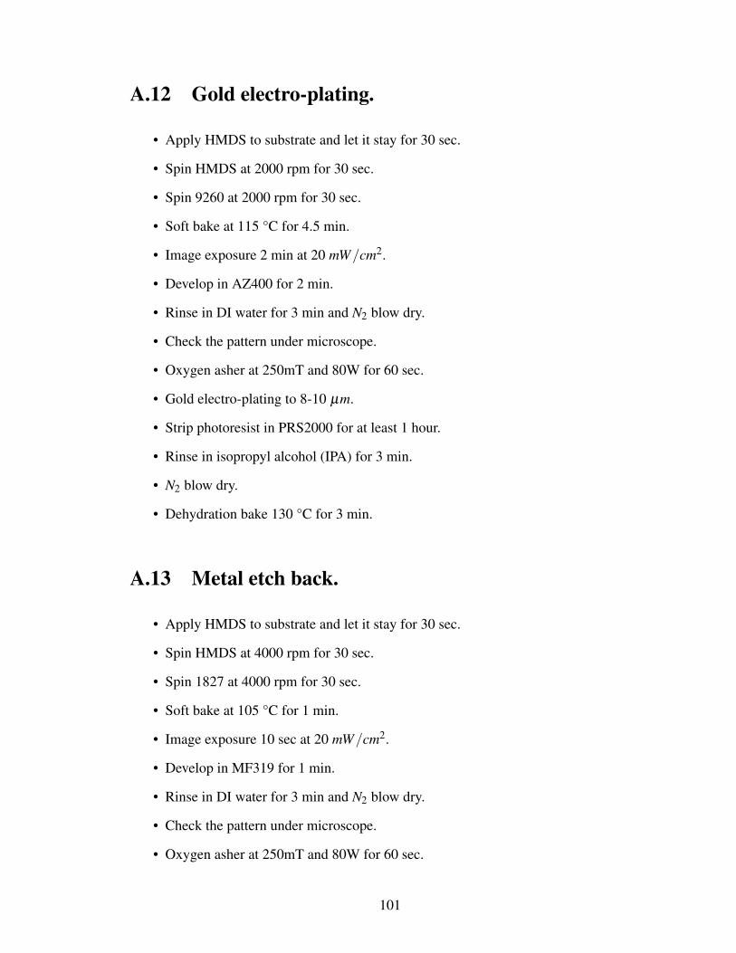
A.12 Gold electro-plating.
• Apply HMDS to substrate and let it stay for 30 sec.
• Spin HMDS at 2000 rpm for 30 sec.
• Spin 9260 at 2000 rpm for 30 sec.
• Soft bake at 115 °C for 4.5 min.
• Image exposure 2 min at 20 mW/cm2.
• Develop in AZ400 for 2 min.
• Rinse in DI water for 3 min and N2 blow dry.
• Check the pattern under microscope.
• Oxygen asher at 250mT and 80W for 60 sec.
• Gold electro-plating to 8-10 µm.
• Strip photoresist in PRS2000 for at least 1 hour.
• Rinse in isopropyl alcohol (IPA) for 3 min.
• N2 blow dry.
• Dehydration bake 130 °C for 3 min.
A.13 Metal etch back.
• Apply HMDS to substrate and let it stay for 30 sec.
• Spin HMDS at 4000 rpm for 30 sec.
• Spin 1827 at 4000 rpm for 30 sec.
• Soft bake at 105 °C for 1 min.
• Image exposure 10 sec at 20 mW/cm2.
• Develop in MF319 for 1 min.
• Rinse in DI water for 3 min and N2 blow dry.
• Check the pattern under microscope.
• Oxygen asher at 250mT and 80W for 60 sec.
101

• Hard bake 110 °C for 1 min.
• Wet etch Au in gold etchant.
• Wet etch Ti in BHF solution.
• Rinse in DI water for 3 min and N2 blow dry.
• Inspect the film thickness by Dektak.
• Strip photoresist in aceton for at least 1 hour.
• Rinse in isopropyl alcohol (IPA) for 3 min.
• N2 blow dry.
• Dehydration bake 130 °C for 3 min.
102

Appendix B
Ferroelectric Thin Film Based Switchable Acoustic Wave Resonatorsand Filters Fabrication Process
B.1 Starting wafer: high resistivity Silicon, 525 µm, with1 µm thermal silicon dioxide.
• Dice and blow dry using N2 gas.
• Rinse in aceton for 3 min.
• Rinse in isopropyl alcohol (IPA) for 3 min.
• Rinse in the DI water for 5 min.
• N2 blow dry.
• Dehydration bake 130 °C for 3 min.
B.2 Bottom electrode evaporation and liftoff.
• Apply HMDS to substrate and let it stay for 30 sec.
• Spin HMDS at 4000 rpm for 30 sec.
• Spin 1813 at 4000 rpm for 30 sec.
• Soft bake at 105 °C for 1 min.
• Soak in chlorobenzen (CBZ) for 5 min.
• Image exposure 10 sec at 20 mW/cm2.
• Develop in MF319 for 1 min.
• Rinse in DI water for 3 min and N2 blow dry.
• Check the pattern under microscope.
103

• Oxygen asher at 250mT and 80W for 60 sec.
• Metal evaporation (Ti/Pt 30/1000 A).
• Liftoff in Acetone for at least 1 hour.
• Rinse in isopropyl alcohol (IPA) for 3 min.
• N2 blow dry.
• Dehydration bake 130 °C for 3 min.
B.3 SiO2 wet etch.
• Apply HMDS to substrate and let it stay for 30 sec.
• Spin HMDS at 4000 rpm for 30 sec.
• Spin 1827 at 4000 rpm for 30 sec.
• Soft bake at 105 °C for 1 min.
• Image exposure 10 sec at 20 mW/cm2.
• Develop in MF319 for 1 min.
• Rinse in DI water for 3 min and N2 blow dry.
• Check the pattern under microscope.
• Oxygen asher at 250mT and 80W for 60 sec.
• Hard bake 110 °C for 1 min.
• Wet etch in BHF solution.
• Rinse in DI water for 3 min and N2 blow dry.
• Inspect the film thickness by Dektak.
• Strip photoresist in aceton for at least 1 hour.
• Rinse in isopropyl alcohol (IPA) for 3 min.
• N2 blow dry.
• Dehydration bake 130 °C for 3 min.
104

B.4 Ferroelectric thin film deposition by PLD.
• Load the substrate and heat up the substrate with 5 °C/min rate.
• Substrate temperature of 650 °C.
• Partial oxygen pressure of 300 mTorr.
• Laser fluence of 1 J/cm2
• In chamber oxygen annealing at 650 °C with 100 Torr oxygen for 1 hour.
• Cool down the substrate with 2 °C/min rate.
B.5 Top electrode evaporation and liftoff.
• Apply HMDS to substrate and let it stay for 30 sec.
• Spin HMDS at 4000 rpm for 30 sec.
• Spin 1813 at 4000 rpm for 30 sec.
• Soft bake at 105 °C for 1 min.
• Soak in chlorobenzen (CBZ) for 5 min.
• Image exposure 10 sec at 20 mW/cm2.
• Develop in MF319 for 1 min.
• Rinse in DI water for 3 min and N2 blow dry.
• Check the pattern under microscope.
• Oxygen asher at 250mT and 80W for 60 sec.
• Metal evaporation (Pt 1000 A).
• Liftoff in Acetone for at least 1 hour.
• Rinse in isopropyl alcohol (IPA) for 3 min.
• N2 blow dry.
• Dehydration bake 130 °C for 3 min.
105
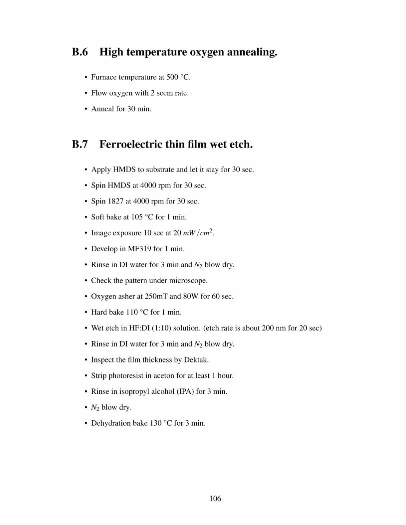
B.6 High temperature oxygen annealing.
• Furnace temperature at 500 °C.
• Flow oxygen with 2 sccm rate.
• Anneal for 30 min.
B.7 Ferroelectric thin film wet etch.
• Apply HMDS to substrate and let it stay for 30 sec.
• Spin HMDS at 4000 rpm for 30 sec.
• Spin 1827 at 4000 rpm for 30 sec.
• Soft bake at 105 °C for 1 min.
• Image exposure 10 sec at 20 mW/cm2.
• Develop in MF319 for 1 min.
• Rinse in DI water for 3 min and N2 blow dry.
• Check the pattern under microscope.
• Oxygen asher at 250mT and 80W for 60 sec.
• Hard bake 110 °C for 1 min.
• Wet etch in HF:DI (1:10) solution. (etch rate is about 200 nm for 20 sec)
• Rinse in DI water for 3 min and N2 blow dry.
• Inspect the film thickness by Dektak.
• Strip photoresist in aceton for at least 1 hour.
• Rinse in isopropyl alcohol (IPA) for 3 min.
• N2 blow dry.
• Dehydration bake 130 °C for 3 min.
106
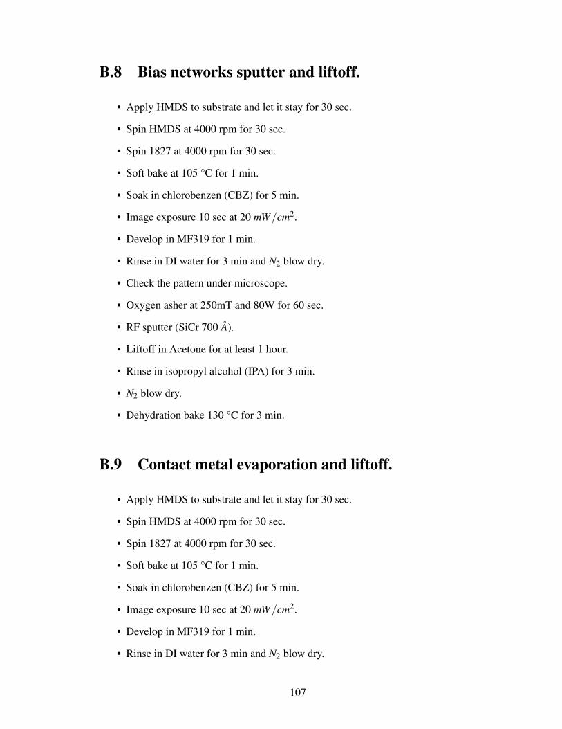
B.8 Bias networks sputter and liftoff.
• Apply HMDS to substrate and let it stay for 30 sec.
• Spin HMDS at 4000 rpm for 30 sec.
• Spin 1827 at 4000 rpm for 30 sec.
• Soft bake at 105 °C for 1 min.
• Soak in chlorobenzen (CBZ) for 5 min.
• Image exposure 10 sec at 20 mW/cm2.
• Develop in MF319 for 1 min.
• Rinse in DI water for 3 min and N2 blow dry.
• Check the pattern under microscope.
• Oxygen asher at 250mT and 80W for 60 sec.
• RF sputter (SiCr 700 A).
• Liftoff in Acetone for at least 1 hour.
• Rinse in isopropyl alcohol (IPA) for 3 min.
• N2 blow dry.
• Dehydration bake 130 °C for 3 min.
B.9 Contact metal evaporation and liftoff.
• Apply HMDS to substrate and let it stay for 30 sec.
• Spin HMDS at 4000 rpm for 30 sec.
• Spin 1827 at 4000 rpm for 30 sec.
• Soft bake at 105 °C for 1 min.
• Soak in chlorobenzen (CBZ) for 5 min.
• Image exposure 10 sec at 20 mW/cm2.
• Develop in MF319 for 1 min.
• Rinse in DI water for 3 min and N2 blow dry.
107

• Check the pattern under microscope.
• Oxygen asher at 250mT and 80W for 60 sec.
• Metal evaporation (Ti/Al/Ti/Au 500/15000/500/5000 A).
• Liftoff in Acetone for at least 1 hour.
• Rinse in isopropyl alcohol (IPA) for 3 min.
• N2 blow dry.
• Dehydration bake 130 °C for 3 min.
B.10 Silicon Micromechining Process
B.10.1 First generation: back side deep reactive ion etching (DRIE)using STS
• Apply HMDS to substrate and let it stay for 30 sec.
• Spin HMDS at 2000 rpm for 30 sec.
• Spin 9260 at 2000 rpm for 30 sec.
• Soft bake at 115 °C for 4.5 min.
• Back side alignment and image exposure 2 min at 20 mW/cm2.
• Develop in AZ400 for 2 min.
• Rinse in DI water for 3 min and N2 blow dry.
• Check the pattern under microscope.
• Oxygen asher at 250mT and 80W for 60 sec.
• Bond with another silicon wafer using 1827.
• Bake in oven at 120 °C for 30 min.
• DRIE silicon etch using STS (etch 500 µm silicon for 2.5 hours).
• Inspect the wafer using Zygo for etch rate.
• Strip photoresit in PRS2000 overnight.
• Rinse in isopropyl alcohol (IPA) for 3 min.
108
• Spin dry the wafer.
• Dehydration bake 130 °C for 3 min.
B.10.2 Second generation: top side etching using XeF2
• Silicon etch using XeF2.
• Inspect the wafer under microscope.
109

Bibliography
110
[1] Y. Lu, “Rf mems devices and their applications in reconfigurable rf/microwave cir-cuits,” Ph.D. dissertation, University of Michigan, 2005.
[2] J. Wang, Z. Ren, and C. T.-C. Nguyen, “1.156-ghz self-aligned vibrating microme-chanical disk resonator,” IEEE Trans. Ultrason., Ferroelectr., Freq. Control, vol. 51,no. 12, pp. 1607–1628, Dec. 2004.
[3] (2008) The apple inc. website. [Online]. Available: http://www.apple.com/iphone
[4] (2008) Ee times. [Online]. Available: http://www.eetimes.com
[5] J. Uher and W. J. R. Hoefer, “Tunable microwave and millimeter-wave bandpass fil-ters,” IEEE Trans. Microw. Theory Tech., vol. 39, pp. 643–653, Apr. 1991.
[6] E. R. Brown, “Rf-mems switches for reconfigurable integrated circuits,” IEEE Trans.Microw. Theory Tech., vol. 46, no. 11, pp. 1868–1880, Nov. 1998.
[7] A. Tombak, J. P. Maria, F. T. Ayguavives, Z. Jin, G. T. Stauf, A. I. Kingon, andA. Mortazawi, “Voltage controlled rf filters employing thin film barium strontiumtitanate tunable capacitors,” IEEE Trans. Microw. Theory Tech., vol. 51, no. 2, pp.462–467, Feb. 2003.
[8] A. Miras and E. Legros, “High-gain frequency-tunable low-noise amplifiers for 38-42.5 ghz band applications,” IEEE Microw. Guided Wave Lett., vol. 7, no. 9, pp.305–307, 1997.
[9] “Cognitive radio and management of spectrum and radio resources in reconfigurablenetworks,” White Paper, Wireless world research forum working group 6, 2005.
[10] J. Mitola, “Cognitive radio for flexible mobile multimedia communications,” in 1999IEEE International Workshop on Mobile Multimedia Communications, 1999, pp. 3–10.
[11] (2008) The akon inc. website. [Online]. Available: http://www.akoninc.com
[12] A. G. Fox, “An adjustable waveguide phase changer,” in Proc. IRE, vol. 35, Dec.1947, pp. 1489–1498.
[13] F. Reggia and E. G. Spencer, “A new technique in ferrite phase shifting for beamscanning of microwave antennas,” in Proc. IRE, vol. 45, Nov. 1957, pp. 1510–1517.
[14] K. M. Johnson, “Microwave varactor tuned transistor oscillator design,” IEEE Trans.Microw. Theory Tech., vol. 14, no. 11, pp. 564–572, Nov. 1965.
[15] Y. Lu, L. P. B. Katehi, and D. Peroulis, “High-power mems varactors and impedancetuners for millimeter-wave applications,” IEEE Trans. Microw. Theory Tech., vol. 53,no. 11, pp. 3672–3678, Nov. 2005.
111
[16] R. York, A. Nagra, E. Erker, T. Taylor, P. Periaswamy, J. Speck, S. Streiffer, andO. Auciello, “Microwave integrated circuits using thin-film bst,” in Proc. Of 12thannual International Symp. On Applications of Ferroelectrics, vol. 1, 2000, pp. 195–200.
[17] G. Rebeiz and J. B. Muldavin, “Rf mems switches and switch circuits,” IEEE Trans.Magn., vol. 2, no. 4, pp. 59–71, 2001.
[18] D. Peroulis, K. Sarabandi, and L. P. B. Katehi, “Low contact resistance series memsswitches,” in 2002 IEEE MTT-S Int. Microwave Symp. Dig., vol. 1, Jun. 2002, pp.223–226.
[19] F. Bannon, J. Clark, and C.-C. Nguyen, “High frequency micromechanical filters,”IEEE J. Solid-State Circuits, vol. 35, no. 4, pp. 512–526, Apr. 2000.
[20] M. Abdelmoneum, M. Demirci, and C.-C. Nguyen, “Stemless wine-glass-mode diskmicromechanical resonators,” in Proc 16th IEEE International MEMS Conference,Jan. 2003, pp. 698–701.
[21] S.-S. Lin, Z. R. Y.-W. Lin, and C. Nguyen, “Self-switching vibrating micromechani-cal filter bank,” in IEEE joint Int. Freq. Contr./Precision Time and Time Interval Symp,Aug. 2005, pp. 135–141.
[22] J.-S. Fu, X. A. Zhu, J. D. Phillips, and A. Mortazawi, “Improving linearity offerroelectric-based microwave tunable circuits,” IEEE Trans. Microw. Theory Tech.,vol. 55, no. 2, pp. 354–360, Feb. 2007.
[23] Z. Jin, A. Tombak, J. P. Maria, B. Boyette, G. T. Stauf, A. I. Kingon, and A. Mor-tazawi, “Microwave characterization of thin film bst material using a simple measure-ment technique,” in 2002 IEEE MTT-S Int. Microwave Symp. Dig., vol. 2, Jun. 2002,pp. 1201–1204.
[24] H.-T. Lue and T.-Y. Tseng, “Application of on-wafer trl calibration on the measure-ment of microwave properties of ba0.5sr0.5tio3 thin films,” IEEE Trans. Ultrason.,Ferroelectr., Freq. Control, vol. 48, no. 6, pp. 1640–1647, Nov. 2001.
[25] P. M. Suherman, T. J. Jackson, and M. J. Lancaster, “Comparison of techniques formicrowave characterization of bst thin films,” IEEE Trans. Microw. Theory Tech.,vol. 55, no. 2, pp. 397–401, Feb. 2007.
[26] R. A. Pucel, “Design considerations for monolithic microwave circuits,” IEEE Trans.Microw. Theory Tech., vol. 29, no. 6, pp. 513–534, Jun. 1981.
[27] K. Ikuta, Y. Umeda, and Y. Ishii, “Measurement of high-frequency dielectric charac-teristics in the mm-wave band for dielectric thin-films on semiconductor substrates,”Journal of Japanese Applied Physics, vol. 34, pp. 1211–1213, 1995.
112

[28] X. Zhu, D.-Y. Chen, Z. Jin, J. D. Phillips, and A. Mortazawi, “Characterization of thinfilm bst tunable capacitors using a simple two port measurement technique,” in 2005IEEE MTT-S Int. Microwave Symp. Dig., Jun. 2005, pp. 611–614.
[29] United Kingdom Accreditation Service 1997 The expression of uncertainty and confi-dence in measurement, M3003 Feltham Std.
[30] Vector network analyzer uncertainty calculator. Agilent Technologies. Version4.7.0.8.
[31] N. Izyumskaya, V. Avrutin, X. Gu, U. Ozgur, B. Xiao, T. Kang, H. Lee, andH. Morkoc, “Growth of high-quality pzt films by peroxide mbe and their optical andstructural characteristics,” in 2007 Mater. Res. Soc. Symp. Proc., 2007.
[32] J. P. Maria, B. A. Boyette, A. I. Kingon, C. Ragaglia, and G. Stauf, “Low losstungsten-based electrode technology for microwave frequency bst varactors,” Journalof Electroceramics, vol. 14, pp. 75–81, 2005.
[33] D. Wu, A. Li, H. Ling, X. Yin, C. Ge, M. Wang, and N. Ming, “Preparation of bstthin films by sol-gel method with rapid thermal annealing,” Applied Surface Science,vol. 165, pp. 309–314, 2000.
[34] J.-L. Wang, Y.-S. Lai, D.-C. Shye, C.-C. Chou, B.-S. Chiou, C.-P. Juan, and H.-C.Cheng, “Dependence of ferroelectric characteristics on the deposition temperature of(pb,sr)tio3 films,” Jpn. J. Appl. Phys., vol. 46, pp. 6727–6732, 2007.
[35] M. J. Dalberth, R. E. Stauber, J. C. Price, C. T. Rogers, and D. Galt, “Improved lowfrequency and microwave dielectric response in strontium titanate thin films grownby pulsed laser ablation,” Appl. Phys. Lett., vol. 72, no. 4, pp. 507–509, Jan. 1998.
[36] A. Vorobiev, P. Rundqvist, and K. Khamchane, “Microwave loss mechanisms inba0.25sr0.75tio3 thin film varactors,” Journal of Applied Physics, vol. 96, no. 8, pp.4642–4649, Oct. 2004.
[37] J.-H. Joo, J.-M. Seon, Y.-C. Jeon, K.-Y. Oh, J.-S. Roh, and J.-J. Kim, “Improvementof leakage currents of pt/(ba,sr)tio3/pt capacitors,” Appl. Phys. Lett., vol. 70, no. 22,pp. 3053–3055, Jun. 1997.
[38] W. Chang, J. S. Horwitz, A. C. Carter, J. M. Pond, S. W. Kirchoefer, C. W.Gilmore, and D. B. Chrisey, “The effect of annealing on the microwave propertiesof ba0.5sr0.5tio3 thin films,” Appl. Phys. Lett., vol. 74, no. 7, pp. 1033–1035, Feb.1999.
[39] Y. R. Liu, P. T. Lai, G. Q. Li, B. Li, J. B. Peng, and H. B. Lo, “Effects of post-deposition oxygen annealing on tuning properties of ba0.8sr0.2tio3 thin-film capaci-tors for microwave integrated circuits,” Materials Chemistry and Physics, vol. 94, pp.114–118, 2005.
113
[40] J. Fu, X. Zhu, D. Chen, J. Philips, and A. Mortazawi, “A linearity improvement tech-nique for thin-film barium strontium titanate capacitors,” in 2006 IEEE MTT-S Int.Microwave Symp. Dig., 2006, pp. 560–563.
[41] J.-S. Fu, X. Zhu, J. Philips, and A. Mortazawi, “A ferroelectric-based impedance tunerfor adaptive matching applications,” in 2008 IEEE MTT-S Int. Microwave Symp. Dig.,2008, pp. 955–958.
[42] A. . Abbaspour-Tamijani, L. Dussopt, and G. M. Rebeiz, “Miniature and tunable fil-ters using mems capacitors,” IEEE Trans. Microw. Theory Tech., vol. 51, no. 7, pp.1878–1885, Jul. 2003.
[43] K. Entesari and G. M. Rebeiz, “A differential 4-bit 6.5-10-ghz rf mems tunable filter,”IEEE Trans. Microw. Theory Tech., vol. 53, no. 3, pp. 1103–1110, Mar. 2005.
[44] I. Vendik, O. Vendik, V. Pleskachev, A. Svishchev, and R. Worderweber, “Designof tunable ferroelectric filters with a constant fractional bandwidth,” in 2001 IEEEMTT-S Int. Microwave Symp. Dig., vol. 3, May 2001, pp. 1461–1464.
[45] J. Nath, D. Ghosh, J. P. Maria, A. I. Kingon, W. Fathelbab, P. D. Franzon, and M. B.Steer, “An electronically tunable microstrip bandpass filter using thin-film barium-strontium-titanate (bst) varactors,” IEEE Trans. Microw. Theory Tech., vol. 53, no. 9,pp. 2707–2712, Sep. 2005.
[46] A. Tombak, F. T. Ayguavives, J. P. Maria, G. T. Stauf, A. I. Kingon, and A. Mor-tazawi, “Tunable rf filters using barium strontium titanate based capacitors,” in 2001IEEE MTT-S Int. Microwave Symp. Dig., vol. 3, May 2001, pp. 1453–1456.
[47] M. Makimoto and M. Sagawa, “Varactor tuned bandpass filters using microstrip-linering resonators,” in 1986 IEEE MTT-S Int. Microwave Symp. Dig., 1986, pp. 411–414.
[48] J. S. Hong and M. J. Lancaster, Microstrip Filters for RF/Microwave Applications.New York: J. Wiley and Sons, 2001.
[49] Ie3d. Zeland Software Inc. Fremont, CA. Release 11.
[50] G. Zheng, J. Papapolymerou, and M. M. Tentzeris, “Wideband coplanar waveguide rfprobe pad to microstrip transitions without via holes,” IEEE Microw. Wireless Com-pon. Lett., vol. 13, no. 12, Dec. 2003.
[51] W. P. Mason, “Electrostrictive effect in barium titanate ceramics,” Phys. Rev., vol. 74,pp. 1134–1147, Nov. 1948.
[52] S. Roberts, “Dielectric and piezoelectric properties of barium titanate,” Phys. Rev.,vol. 71, pp. 890–895, Jun. 1947.
[53] S. Tappe, U. Bottger, and R. Waser, “Electrostrictive resonances in (ba0.7sr0.3)tio3thin films at microwave frequencies,” Appl. Phys. Lett., vol. 85, pp. 624–626, Jul.2005.
114

[54] S. Gevorgian, A. Vorobiev, and T. Lewin, “Dc field and temperature dependentacoustic resonances in parallel capacitors based on srtio3 and ba0.25sr0.75tio3 films:experiment and modeling,” J. Applied Phys., vol. 99, p. 12411, 2006.
[55] K. Lakin, G. Kline, and K. McCarron, “High-q microwave acoustic resonators andfilters,” IEEE Trans. Microw. Theory Tech., vol. 41, no. 12, pp. 2139–2146, Dec.1993.
[56] J. Larson, S. W. P. Bradley, and R. Ruby, “Modified butter-worth dyke circuit forfbar resonators and automated measurement system,” in 2000 IEEE Ultrasonic Symp.,2000, pp. 863–868.
[57] J. Park, H. Lee, K. Lee, H. Lee, and Y. Ko, “Micromachined fbar rf filters for advancedhandsets applications,” in 12th International conference on transducers, solid-statesensors, actuators and microsystems, vol. 1, Jun. 2003, pp. 911–914.
[58] R. Ruby, “Review and comparison of bulk acoustic wave fbar smr technology,” in2007 IEEE Ultrasonic Symp., Oct. 2007, pp. 1029–1040.
[59] D. R. Chase, L. Y. Chen, and R. A. York, “Modeling the capacitive nonlinearity in thinfilm bst varactors,” IEEE Trans. Microw. Theory Tech., vol. 53, no. 10, pp. 3215–3220,Oct. 2005.
[60] G. Piazza, P. J. Stephanou, and A. P. Pisano, “Piezoelectric aluminum nitride vibrat-ing contour mode mems resonators,” J. Microelectromech. Syst., vol. 15, no. 6, pp.1406–1418, Dec. 2006.
[61] J. Berge, A. Vorobiev, W. Steichen, and S. Gevorgian, “Tunable solidly mounted thinfilm bulk acoustic resonators based on basrtio3 films,” IEEE Microw. Wireless Com-pon. Lett., vol. 17, no. 9, pp. 655–657, 2007.
[62] M. Vehkamaki, T. Hanninen, M. Ritala, M. Leskela, T. Sajavaara, E. Rauhala, andJ. Keinonen, “Atomic layer deposition of srtio3 thin film from a novel strontium pre-cursor strontium-bis(tri-isopropylcyclopentadienyl),” Chem. Vap. Depos., vol. 7, pp.75–80, 2001.
[63] M. Vehkamaki, T. Hatanpaa, T. Hanninen, M. Ritala, and M. Leskela, “Growth ofsrtio3 and batio3 thin films by atomic layer deposition,” Electrochemical and Solid-State letters, vol. 2, pp. 504–506, 1999.
[64] P. Stephanou and A. Pisano, “Ghz higher order contour mode aln annular resonators,”in IEEE 20th International conference on MEMS, Jan. 2007, pp. 787–790.
[65] S. Schneider, T. Mono, B. Albrethsen-Keck, Y. Melaku, and R. Waser, “Dry-etchingof barium strontium titanate thin films,” in ISAF 98 Proceeding of the 11th IEEEInternational Symposium on Applications of Ferroelectrics, Aug. 1998, pp. 51–54.
[66] G. H. Kim, K. T. Kim, and C. I. Kim, “Dry etching of (ba,sr)tio3 thin films usingan inductively coupled plasma,” J. Vac. Sci. Technol. A, vol. 23, no. 4, pp. 894–897,2005.
115


![Sangeetha [Ferroelectric Memory]](https://img.dokumen.tips/doc/110x75/55cf8f91550346703b9d9665/sangeetha-ferroelectric-memory.jpg)