Embed Size (px)
Citation preview
HAL Id: tel-00913379https://tel.archives-ouvertes.fr/tel-00913379v2
Submitted on 26 Jun 2014
HAL is a multi-disciplinary open accessarchive for the deposit and dissemination of sci-entific research documents, whether they are pub-lished or not. The documents may come fromteaching and research institutions in France orabroad, or from public or private research centers.
L’archive ouverte pluridisciplinaire HAL, estdestinée au dépôt et à la diffusion de documentsscientifiques de niveau recherche, publiés ou non,émanant des établissements d’enseignement et derecherche français ou étrangers, des laboratoirespublics ou privés.
Surface plasmon hybridization in the strong couplingregime in gain structures
Aurore Castanié
To cite this version:Aurore Castanié. Surface plasmon hybridization in the strong coupling regime in gain structures.Other [cond-mat.other]. Université Montpellier II - Sciences et Techniques du Languedoc, 2013. En-glish. NNT : 2013MON20093. tel-00913379v2

UNIVERSITE MONTPELLIER II
SCIENCES ET TECHNIQUES DU LANGUEDOC
THESE
pour obtenir le grade de
DOCTEUR DE L’UNIVERSITE MONTPELLIER II
Discipline : Physique de la Matiere Condensee
Ecole Doctorale : Information, Structures, Systemes
presentee et soutenue publiquement
par
Aurore Castanie
le 4 octobre 2013
Titre :
Surface Plasmon Hybridization in The StrongCoupling Regime in Gain Structures
JURY
Prof. Dominique Barchiesi Universite de Technologie de Troyes President du juryProf. Alexey Kavokin University of Southampton RapporteurProf. Joel Bellessa Universite Lyon 1 RapporteurD.R. Philippe Ben-Abdallah Institut d’Optique ExaminateurProf. Didier Felbacq Universite Montpellier 2 Directeur de theseProf. Brahim Guizal Universite Montpellier 2 Directeur de theseMcf. Mauro Antezza Universite Montpellier 2 Examinateur


Acknowledgements
These three years of doctorate have been a really great, professional and personal,
experience. First, I wish to thank Alexey Kavokin and Joel Bellessa for spending
time to read my works, and Dominique Barchiesi, Philippe Ben-Abdallah and
Mauro Antezza for doing me the honor of agreeing to be part of my examination
committee.
Je tiens tout particulierement a remercier mes directeurs de these, Brahim
Guizal et Didier Felbacq pour m’avoir guidee dans mes recherches et m’avoir appris
tant de choses. Ce fut veritablement une experience tres enrichissante pour moi.
Je souhaite tout autant remercier mes collegues de travail avec lesquels j’ai partage
un bureau et de nombreuses conversations informelles.
Je remercie ma famille pour son soutien et sa patience durant ces trois annees
et meme durant celles qui les ont precedees ! Merci a Richard pour sa presence
et le sacrifice de vacances d’ete au profit de ma (nos !) redaction(s). J’espere
aussi t’avoir apporte mon soutien et continuer a le faire. Merci a Elisabeth pour
ses conseils, a Dominique pour ses corrections d’anglais, a Olivia, a Marie, a mon
Pere, a ma Mere... Merci en somme.
i

ii

Contents
Acknowledgements i
Contents iii
Introduction vii
1 Theoretical and Numerical Tools 1
1.1 Wave equation . . . . . . . . . . . . . . . . . . . . . . . . . . . . . 1
1.1.1 Maxwell’s equations . . . . . . . . . . . . . . . . . . . . . . 1
1.1.2 Solution of the wave equation . . . . . . . . . . . . . . . . . 3
1.2 Wave propagation in a stratified medium . . . . . . . . . . . . . . . 5
1.2.1 Propagation equations . . . . . . . . . . . . . . . . . . . . . 6
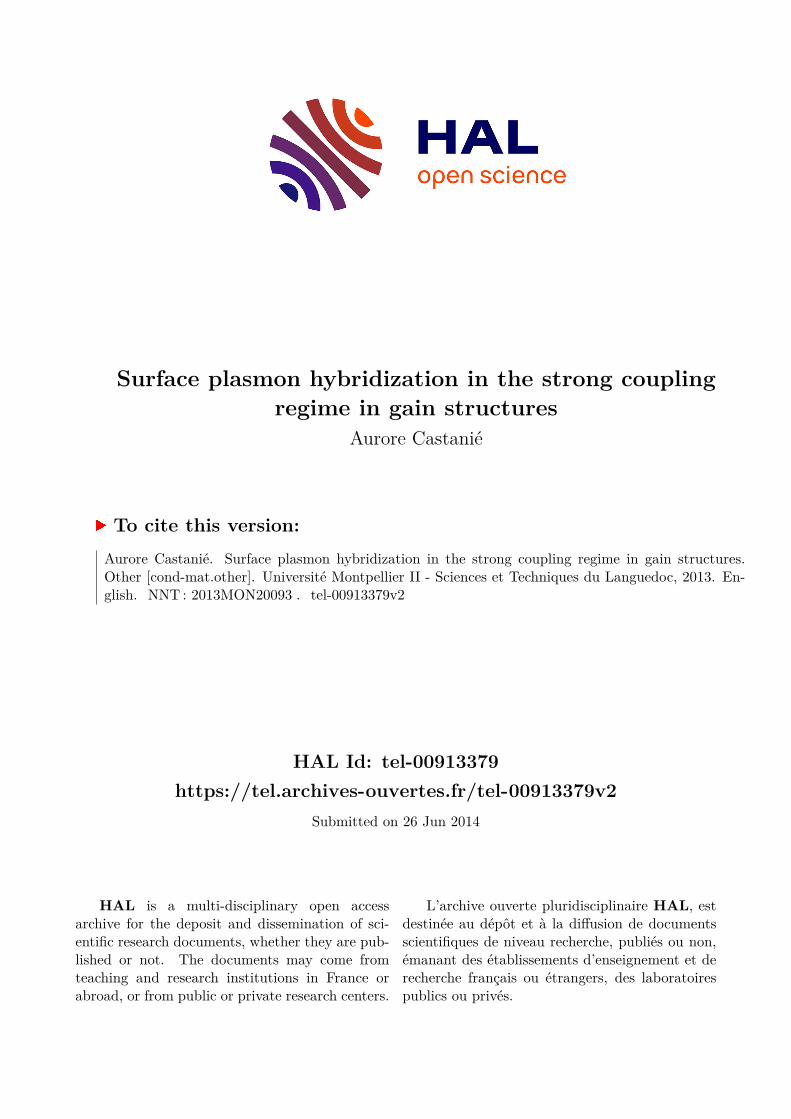
1.2.2 The Transfer matrix method . . . . . . . . . . . . . . . . . . 8
1.2.3 The Scattering matrix method . . . . . . . . . . . . . . . . . 9
1.3 The polology theory . . . . . . . . . . . . . . . . . . . . . . . . . . 12
1.3.1 Cauchy’s integral formula and Laurent series . . . . . . . . . 12
1.3.2 Residue theorem . . . . . . . . . . . . . . . . . . . . . . . . 14
1.3.3 Branch points and cut lines . . . . . . . . . . . . . . . . . . 16
1.4 The tetrachotomy method . . . . . . . . . . . . . . . . . . . . . . . 19
1.4.1 Poles of a meromorphic function . . . . . . . . . . . . . . . . 19
1.4.2 Application . . . . . . . . . . . . . . . . . . . . . . . . . . . 24
2 Coupling Surface Plasmon Polaritons 27
2.1 Surface plasmon polaritons at a single interface . . . . . . . . . . . 28
2.1.1 Existence conditions . . . . . . . . . . . . . . . . . . . . . . 28
2.1.2 The dispersion relation . . . . . . . . . . . . . . . . . . . . . 31
2.1.3 SP length scales . . . . . . . . . . . . . . . . . . . . . . . . 33
iii

iv CONTENTS
2.2 Dielectric permittivity of metals . . . . . . . . . . . . . . . . . . . 37
2.3 Metallic film in non-symmetric medium . . . . . . . . . . . . . . . . 39
2.3.1 Optical coupling of SPs . . . . . . . . . . . . . . . . . . . . 39
2.3.2 ATR configuration . . . . . . . . . . . . . . . . . . . . . . . 44
2.4 Metallic film in symmetric media . . . . . . . . . . . . . . . . . . . 46
2.4.1 The dispersion relations . . . . . . . . . . . . . . . . . . . . 47
2.4.2 Review on LRSPs . . . . . . . . . . . . . . . . . . . . . . . . 48
2.4.3 Comparison of the length scales . . . . . . . . . . . . . . . . 50
2.5 Theoretical LRSP on PECS . . . . . . . . . . . . . . . . . . . . . . 50
2.5.1 Reviewed image charge theory . . . . . . . . . . . . . . . . . 51
2.5.2 Equivalence of the structures . . . . . . . . . . . . . . . . . 53
3 Coupling Dielectric Waveguides 57
3.1 Symmetric dielectric waveguides . . . . . . . . . . . . . . . . . . . . 57
3.1.1 Expression of the modes . . . . . . . . . . . . . . . . . . . . 58
3.1.2 Graphical solutions . . . . . . . . . . . . . . . . . . . . . . . 60
3.1.3 Low and high frequency limits . . . . . . . . . . . . . . . . . 62
3.2 Coupled dielectric waveguides . . . . . . . . . . . . . . . . . . . . . 63
3.2.1 Coupling of modes in time . . . . . . . . . . . . . . . . . . . 64
3.2.2 Coupling optical waveguides . . . . . . . . . . . . . . . . . . 67
3.3 PT-Symmetry . . . . . . . . . . . . . . . . . . . . . . . . . . . . . . 77
3.3.1 In quantum mechanics . . . . . . . . . . . . . . . . . . . . . 77
3.3.2 In optics . . . . . . . . . . . . . . . . . . . . . . . . . . . . . 79
3.3.3 Numerical application . . . . . . . . . . . . . . . . . . . . . 82
4 Strong Coupling Surface Plasmon Polaritons 87
4.1 Classical coupled oscillators . . . . . . . . . . . . . . . . . . . . . . 88
4.1.1 Strong coupling transition . . . . . . . . . . . . . . . . . . . 88
4.1.2 Temporal oscillations . . . . . . . . . . . . . . . . . . . . . . 91
4.1.3 Anticrossing of the dispersion curves . . . . . . . . . . . . . 93
4.2 Microcavity polaritons . . . . . . . . . . . . . . . . . . . . . . . . . 94
4.2.1 Definition in quantum physics . . . . . . . . . . . . . . . . . 94
4.2.2 Review on the strong coupling regime . . . . . . . . . . . . . 99
4.3 Strongly coupled SP and guided modes . . . . . . . . . . . . . . . . 104
4.3.1 The device . . . . . . . . . . . . . . . . . . . . . . . . . . . . 104

CONTENTS v
4.3.2 Variation of the characteristic parameters . . . . . . . . . . 106
4.3.3 Numerical results for the optimal coupling . . . . . . . . . . 112
4.4 Adding gain in the strongly coupled structure . . . . . . . . . . . . 119
4.4.1 Adding gain in the core of the waveguide . . . . . . . . . . . 120
4.4.2 Adding gain in the medium between the two strongly cou-
pled modes . . . . . . . . . . . . . . . . . . . . . . . . . . . 122
4.4.3 Adding gain without a strong coupling device . . . . . . . . 127
Conclusion 129
A 2D dispersive FDTD 131
B Resume en francais 141
C Abstract in English 155
Bibliography 157

vi CONTENTS

Introduction
Nanophotonics and micro-optics had a remarkable impact on all kinds of applica-
tions in communications, sensing, imaging, data storage, etc [1]... However, the
size of a dielectric waveguide is still ruled by the diffraction limit (λ/(2n), n being
the guide refractive index and λ being the free space wavelength of the incident
wave). It has been discovered that waveguides based on surface plasmon polaritons
can support propagation modes tightly bounded to the metallic surfaces and con-
fine the waves in deep sub-wavelength scales. Accordingly, plasmonics has received
tremendous attention for its scope to overcome the diffraction limit. In order to
present the context and the perspective of this work, it is appropriate to start out
with a short introduction to the plasmonics’ research history.
Plasmonics is a branch of nanophotonics devoted to the study of surface plas-
mon polaritons (SPs) and their applications. In 1902, R. W. Wood [2] observed
sudden variations of the intensity in the light beam spectrum, reflected by a diffrac-
tion grating under the transverse magnetic polarization. According to him, the
intensity of the incident beam being continuous, the reflected spectrum had to be
continuous too. These variations are strongly dependent on the incident angle of
the light beam, and it was demonstrated later that they are due to the coupling be-
tween the propagating incident waves and the surface plasmons waves. In 1957, R.
H. Ritchie [3] demonstrated theoretically the existence of transverse plasmons on
a metallic surface. In 1958, R. A. Ferrel studied, also theoretically, the coupling of
these modes with an electromagnetic wave and presented the first determination
of the dispersion relation corresponding to electromagnetic waves on a metallic
surface. Using a mono-kinetic electronic beam, C. J. Powell and J. B. Swan [4] ex-
perimentally observed surface plasmon excitations at metallic interfaces. A. Otto
proposed an experimental configuration based of the use on a prism, called the
FTR (Frustrated Total Reflection) configuration, to observe the coupling between
vii

viii INTRODUCTION
an electromagnetic wave and surface plasmons. E. Kretschmann [5] modified and
simplified this geometry towards the well-known ATR (Attenuated Total Reflec-
tion) configuration. It was only in 1989 that it became possible to observe surface
plasmons using Scanning Near-field Optical Microscopy (SNOM) [6, 7].
Research in plasmonics has made very fast progress in the following decades
[8, 9, 10, 11, 12, 13]. In 1998, T. W. Ebbesen et al. [14] described an experiment
in which nanoholes in a silver film allow a great transmission of light through
sub-wavelength nanostructures when the standard aperture theory [15] predicted
a very small light transmission for such small holes. To explain this phenomenon,
different devices were analysed and the experiments showed that this effect persists
on all metals and with a strong angle dependency. It was thus assumed that this
was a SP related effect. This result renewed the interest for studying SPs and
the term plasmonics began to be used shortly after.
Plasmonics have been very beneficial in terms of resolution for lenses [16] since
the studies carried out by J. B. Pendry [17] and by N. Fang et al. [18]. They
are also used to enhance light emission [19] or photovoltaic devices [20]. The
LSPR (localized surface plasmon resonance) allows the electromagnetic field en-
hancement that leads to surface-enhanced Raman scattering (SERS) [21], second
harmonic generation [22] and other surface-enhanced spectroscopic processes [23].
Imaging at the single molecule level has also taken advantage of the enhancement
of the fluorescence on plasmonic surfaces [24, 25] or in solutions containing metal-
lic nanoparticles [26]. At present, the range of plasmonics based biosensors is
dominated by instruments that operate using the Kretschmann arrangement (this
configuration is presented in Section 2.3.1). The physical size of the sensing ele-
ment is limited by the propagation length of the SP . The new approach pursued
now is to combine SPR with other types of guided modes (hybrid sensors). For
instance, in metamaterial arrays of silver nanorods capable of supporting a guided
mode, the interaction between the guided mode and the SPR leads to excellent
sensor performances in the near infrared [27].
In the field of sub-wavelength surface optics, Zhijun et al. [28] presented the
possibility of creating metallic Fresnel-like lenses. These were designed in such a
way that each nanoslit element transmits light with phase retardation controlled
by the metal thickness in the aperture region. The advantage, as compared to
the conventional lenses, is the possibility to control each phase shift separately by

ix
changing the corresponding slit depth.
The SP modes play key roles in today’s nanophotonics [29] and are also used
in many applications such as detection, or in surface optics. However, the intrinsic
losses due to the metal limit their propagation length and thus their applications
[30, 31, 32, 33]. To enhance this propagation length, many possibilities have been
considered. The older one consists in coupling two surface plasmons. When a
metallic film becomes too thin, the two SP modes which are on each interface
between the metal and the dielectric media can interact and there is a coupling
[34, 35, 36]. The result is the creation of two new modes, known as the LRSP
(Long Range Surface Plasmon) which is characterized by a better propagation
length than the SP on a metallic bulk [37] and the SRSP (Short Range Surface
Plasmon) which has a lower propagation length. Going on from there, a large
range of applications [38, 39, 40], such as in photonic crystals, stratified media,
quantum systems or with anisotropy, become possible.
A more recent and famous way to enhance the propagation length of the SP
modes is the use of gain media. These structures involve adding gain in a dielec-
tric medium with a metallic film directly deposited on it [41, 42]. However, the
improvement of the field is limited by the depth penetration of the plasmon in the
two media. Thus, the efficiency of this approach is insufficient.
Another point of view consists in thinking that the SPs are light waves that we
want to amplify as a laser. This possibility has been explored and has been called a
SPASER. It could generate stimulated emission of surface plasmons in resonating
metallic nanostructures adjacent to a gain medium [43, 44]. The light emission
could also be coherent, which can give interesting applications in sub-wavelength
surface optics.
In the same idea, it was reported the use of confined Tamm plasmon modes
towards the realization of nano-lasers [45]. Their advantage in comparison of clas-
sical SP modes is that they can be directly excited with light wave because their
in-plane wave vector is less than the wave vector of light in vacuum. They can
also be formed in both TM and TE polarizations [46, 47]. A first demonstration
of laser emission for Tamm structures is presented in [45].
The configuration we propose here consists of putting gain into the medium
between a SP and a classical waveguide under the regime of the strong coupling.
This regime allows a significant improvement of the SP emission as will be pre-

x INTRODUCTION
sented in this work.
Scope of this thesis
We begin by providing an overview of the theoretical foundations of SPs by the
means of Maxwell’s equations. The aim of this first chapter is to present the tools
used to compute and study multistratified media through both the dispersion and
absorption relations. Thus, we present the transfer and scattering matrix methods,
which are usual methods to study multistratified media. These methods need to be
extended in order to find the modes and to account for the losses of the structure.
The losses lead to a complex dispersion relation. It is also possible to demonstrate
that the existence of solutions corresponds to the maximisation of the determinant
of the scattering matrix, that is to say the poles of this matrix. Thereafter, it is
demonstrated that the poles of a complex function can be found though Cauchy’s
integral theorem. The development of our technique of computation, called the
tetrachotomy method, according to [48] is also presented.
Chapter 2 concerns the definition of the surface plasmon polaritons and their
coupling, when a metallic film supporting two SP modes becomes thin enough to
allow the interaction. To begin, the coupling between a volume plasmon and a pho-
ton generates a surface plasmon. When the collective oscillation of the electrons’
gas is coupled with light at the interface between a metal and a dielectric, we also
talk about surface plasmon polaritons (noted SPs). The SP modes correspond to
solutions of Maxwell’s equations. There are two ways to find them: we can search
solutions corresponding to evanescent waves on both sides of the interface; or we
can search for the response of the structure with the determination of the reflection
and transmission coefficients r and t when an electromagnetic plane wave comes
to hurt the structure.
The scope of this chapter is to present the coupling between SP modes, the
result being the creation of two modes, known as the LRSP (Long Range Surface
Plasmon) which is characterized by better propagation length than the SP on a
metallic bulk, and the SRSP (Short Range Surface Plasmon) defined by a lower
propagation length. The main drawback of using the SP modes resides in their
intrinsic losses, and the LRSP modes can provide a first solution to reduce them.
We finally demonstrate the possibility to excite a LRSP mode without the SRSP

xi
mode on a perfect electric conductor (PEC) substrate. This last possibility is a
first step towards the use of the LRSP for applications such as the detection of
molecules, the experimental realization being possible with a PEC on one side and
vacuum on the other.
In Chapter 3, the coupling between two dielectric waveguides is studied in order
to understand the basic physical mechanisms at play. Dielectric waveguides provide
simple models for the confining mechanism of waves propagating in optical devices.
The coupling of waveguides has been intensively studied, in particular with the
coupled-mode theory [49, 50, 51, 52, 53]. After a reminder concerning the dielectric
slab waveguides, the coupled-mode theory will be presented. This theory can be
derived from the variational principle for the frequencies of the system. When
a trial solution is introduced into the electric field in a lossless electromagnetic
system, such as the linear superposition of modes, the coupled-mode theory gives
the result. The coupled-modes theory is presented both for the transverse electric
and transverse magnetic polarizations, the latter one never having been published.
The last section deals with the case of two optical waveguides respecting the parity
time (PT) symmetry. This symmetry has been evidenced in quantum mechanics
by C. M. Bender [54] but it can also apply to optical devices. Furthermore, a
numerical application is also presented.
The last chapter focuses on the strong coupling regime. This regime has been
particularly studied in microcavities since the work of C. Weisbuch et al. [55]. The
strong coupling is characterized by an anticrossing between the original modes
dispersion relations and by the apparition of a Rabi splitting [56] between the
new modes of the structures. In the first section, the characteristics of the strong
coupling regime are introduced, with the classical case of two coupled oscillators.
Then, the properties of the strong coupling regime in microcavities are presented
until recent works implying surface plasmons. Finally, we demonstrate the strong
coupling regime between SP modes and guided modes in a layered structure. More
precisely, we study the features of the new modes so as to justify the interest of
this kind of structure. Gain is added in order to further enhance the plasmon
emission. In this way, we obtain an improvement of the propagation length for a
hybrid surface plasmon mode (that is still confined on the surface) of more than
six thousand times the length of the strongly coupled case without gain.

xii INTRODUCTION

Chapter 1
Theoretical and Numerical Tools
Overview All the structures we are going to study are stratified media,
thin and smooth films alternated in layers. We study more precisely the
corresponding dispersion relations which allow the determination of the
modes living in the structures and also give information about their inter-
actions. After reminding the wave equation, the propagation equations
in a stratified media are introduced. The transfer matrix (T-matrix)
method is also presented and compared to the scattering matrix (S-
matrix) method. The S-matrix formalism allows to find the coefficients
of reflection R and transmission T but also the modes of the structure.
We demonstrate that it is sufficient to find the poles of the determinant
of the S-matrix to obtain the dispersion curves and the corresponding ab-
sorption curves. The fundamental properties of polology are summed up
and we describe the method we used, namely the tetrachotomy method.
1.1 Wave equation
1.1.1 Maxwell’s equations
Published in 1864, Maxwell’s equations predicted the propagation - even in vacuum
- of electromagnetic waves. More precisely, they predicted a velocity c for these
waves in vacuum. It is possible to demonstrate that this velocity is the speed of
light and only depends on two known constants: c = (µ0ε0)−1/2 with µ0 and ε0 the
1

2 CHAPTER 1. THEORETICAL AND NUMERICAL TOOLS
permeability and the permittivity of the vacuum, respectively1.
In linear, isotropic, homogeneous (LIH) and source-free medium, Maxwell’s
equations are:
∇× E = −∂B
∂t, (1.1)
∇×H =∂D
∂t, (1.2)
∇ ·D = 0, (1.3)
∇ ·B = 0, (1.4)
with εr(x, y, z), the permittivity of the medium. In what follows, we only consider
non-magnetic media, where µ = µ0.
To find a self-consistent solution for the electromagnetic field, Maxwell’s equa-
tions must be supplemented by the constitutive relations that describe the behavior
of matter under the influence of the fields. Thus, the electric displacement field D
is defined by:
D = ε0E+P, (in vacuum D = ε0E). (1.5)
D is used to avoid explicit inclusion of the charge associated with the polarization
P in Gauss’s flux law (Eq. 1.3). Equivalently, we can also write the polarization
P = χε0E, where the electric susceptibility χ is given by χ = εr − 1. Then, the
expression of the magnetic induction field B is:
B = µ0(H+M). (1.6)
In what follows, B will always be replaced by its equivalent µ0H because M = 0
for LIH and non-magnetic medium.
Combining Eqs. 1.1 and 1.2 leads to Helmholtz’s equations for E and H:
1
εr(x, y, z)∇× [∇× E]− ω2
c2E = 0, (1.7)
1By definition, the exact value of µ0 is 4π.10−7 H.m−1 and the measured value of ε0 is8, 854.10−12 F.m−1.

1.1. WAVE EQUATION 3
∇×[
1
εr(x, y, z)∇×H
]
− ω2
c2H = 0, (1.8)
where ω/c = k0 = 2π/λ0 with λ0, the wavelength of light in vacuum.
In the case of metallic media, Ampere’s equation (Eq. 1.2) includes the differ-
ential form of Ohm’s law j = σE, because the conductivity σ 6= 0 (more precisely,
it is not negligibly small). Eq. 1.2 becomes:
∇×H+ iωεE− j = ∇×H+ iω(
ε+ iσ
ω
)
E = 0. (1.9)
To rewrite this equation in its initial form, we have to introduce an effective di-
electric permittivity ε in order to account for the conductivity term σ:
ε = ε+ iσ
ω. (1.10)
In the case of homogeneous metals, ε is constant and independent of the direction
in space, it follows that ∇ · E = 0 is still used. The corresponding Helmholtz’s
equation is also given by Eq. 1.7 with εr(x, y, z) = ε/ε0.
1.1.2 Solution of the wave equation
We consider Maxwell’s equations for vacuum (εr(x, y, z) = 1) in order to obtain
the simplest form of the electromagnetic wave equation and to present the well
known solution of the wave equation. The Ampere and Faraday equations are
rewritten as:
∇× E = −µ0∂H
∂t, (1.11)
∇×H = ε0∂E
∂t. (1.12)
The solutions for E and H can be separated by taking the curl of Eq. 1.11 and the
time derivative of Eq. 1.12. Then, using the fact that the order of differentiation
can be reversed, the two Maxwell’s wave equations are:
∇2E = µ0ε0∂2E
∂t2, (1.13)

4 CHAPTER 1. THEORETICAL AND NUMERICAL TOOLS
∇2H = µ0ε0∂2H
∂t2. (1.14)
These equations are the form:
d2A
dx2=
1
c2d2A
dt2. (1.15)
For simplicity, we only consider the wave propagation in a single spatial direction,
the x-direction. The vector A becomes a function of x and t and may be expressed
as A(x, t). It could represent either the electric field vector E(x, t) or the magnetic
field vector H(x, t). c is still the velocity of light in vacuum.
It is possible to demonstrate that A(x, t) is an oscillatory wave function with
an amplitude that is transverse to the direction of propagation. We assume that
the wave function A(x, t) is separable and thus can be written as a product of
functions Az(z) and At(t). Eq. 1.15 becomes:
c2
Az
d2Az
dz2=
1
At
d2At
dt2. (1.16)
Both sides must be equal to a negative constant−ω2 in order to satisfy the equation2. That leads to the following equations:
d2Ax
dx2+
ω2
c2Ax = 0, (1.17)
d2At
dt2+ ω2At = 0. (1.18)
And the corresponding solutions are:
Ax = c1eikxx + c2e
−ikxx, (1.19)
At = d1eiωt + d2e
−iωt, (1.20)
where the constants c1, c2, d1 and d2 are determined by the boundary conditions
2The consequence of the choice of a positive constant for At(t) would be real exponential thatcannot represent a real field. On the other hand, taking a negative constant leads to periodicfunctions At(t) = e±iωt with ω = kc, so the solutions could be monochromatic waves.

1.2. WAVE PROPAGATION IN A STRATIFIED MEDIUM 5
and the propagation constant kx = ω/c = 2π/λ. Finally, the general solution
involves a complex wave function:
A(x, t) = Ax(x)At(t) ∝ e±i[kxx∓ωt]. (1.21)
The wave described by Eq. 1.21 represents a wave that, for any value of x, has
the same amplitude value for all values of y and z. It is thus referred to as a plane
wave since it represents planes of constant value that are of infinite lateral extent.
We consider a wave travelling from left to right that is a function of the form
A(x, t) = cei(kxx−ωt) and the more general form for A(x, y, z, t) is:
A = A0ei(k·r−ωt). (1.22)
with A the electric or magnetic component of an electromagnetic wave. So, with
this type of solution, ∇ · E = 0 can be associated to ∇ · E = ik · E from Eq.
1.22. That involves ik · E = 0, and thus E is perpendicular to k, the direction
of propagation. The same conclusion is found with the magnetic field H and Eq.
1.4. Hence, these electromagnetic waves are referred to as transverse waves.
1.2 Wave propagation in a stratified medium
All the structures we are going to study are stratified media, thin and smooth
films alternated in layers. More precisely, we study the corresponding dispersion
relations which allow the determination of the modes living in the structures, and
also give information concerning their interactions.
The relation between the angular frequency of an incident wave and the mag-
nitude of its wave vector is the dispersion relation 3. In this work, we will always
consider ω real, and the propagation constant α complex.

6 CHAPTER 1. THEORETICAL AND NUMERICAL TOOLS
N+1
I’
I0
R
T
a1
2
1
p
N
b1
a2 b2
ap bp
aN bN
x
y
Figure 1.1: Stratified medium with layers from 1 to N . We note the outgoing amplitudes Rand T and the incoming ones I and I ′. The intermediate layers have the amplitudes ap and bp(p = 1 . . . N).
1.2.1 Propagation equations
Expression of the field
We consider a stratified medium with layers from 0 to N + 1 (Fig. 1.1) [57]. In
a LIH medium, with the time dependence e−iωt and the TM polarization in the
plane (x, y), we denote the magnetic field as H = H(x, y)ez. The field H(x, y)
satisfies the following Helmholtz’s equation:
div(ε−1j ∇H) + k2
jH = 0, (1.23)
where k2j = k2
0εj is the wave vector in each layer j. This equation has to be solved
separately in regions of constant εj, and the solutions obtained must be matched
using appropriate boundary conditions. We note α and βj the wave vectors in the
3The dispersion relation, ω = ω(α) with α the in-plane component of the wave vector (thepropagation constant), is a linear equation with constant coefficients which determines how thetemporal oscillations exp(−iωt) are linked to the spatial oscillations exp(iαx), with plane wavesexp(iαx) exp(−iω(α)t) as solutions.

1.2. WAVE PROPAGATION IN A STRATIFIED MEDIUM 7
x and the y directions.
We note H(x, y) = eiαxu(y) and the field u(y) in each medium j satisfies:
∂2u
∂y2+ (k2
j − α2)u = 0, (1.24)
The solutions are plane waves ei(k·r−ωt) = ei(αx+βjy−ωt) and the dispersion rela-
tion is given by α2 + β2j = k2
0εj with µr = 1.
The field in the different layers is:
u0(x, y) = Iei(αx+β0y) +Rei(αx−β0y), (1.25)
up(x, y) = apei(αx+βpy) + bpe
i(αx−βpy) with p = 1 . . . N, (1.26)
uN+1(x, y) = Tei(αx+βN+1y) + I ′ei(αx−βN+1y). (1.27)
Before applying the boundary conditions, we can simplify the previous expres-
sions. First, we must impose that there are no incoming waves in the medium of
transmission (N + 1), I ′ = 0. Moreover, the quantity βj is defined in terms of the
quantities kj and α:
βj =
√
k20εj − α2 if | α |< k0
√εj,
i√
α2 − k20εj if | α |> k0
√εj.
(1.28)
The first condition | α |< k0√εj implies that βj is real and corresponds to
propagating waves. The second condition | α |> k0√εj implies that βj is imaginary
and corresponds to evanescent waves. Evanescent waves are solutions that remain
confined in the near vicinity of an interface between two media.
Boundary conditions
We apply the boundary conditions to solve Eqs. 1.25, 1.26 and 1.27 with p =
1 . . . N . For each interface, u and ε−1j ∂yu must be conserved in the TM polariza-
8 CHAPTER 1. THEORETICAL AND NUMERICAL TOOLS
tion. For y = 0:
eiαx(
Ieiβ00 +Re−iβ00)
= eiαx(
a1eiβ10 + b1e
−iβ10)
,
iβ0
ε0eiαx
(
Ieiβ00 −Re−iβ00)
= iβ1
ε1eiαx
(
a1eiβ10 − b1e
−iβ10)
.(1.29)
For y = yp:
eiαx(
apeiβpyp + bpe
−iβpyp)
= eiαx(
ap+1eiβp+1yp + bp+1e
−iβp+1yp)
,
iβp
εpeiαx
(
apeiβpyp − bpe
−iβpyp)
= iβp+1
εp+1eiαx
(
ap+1eiβp+1yp − bp+1e
−iβp+1yp)
.
(1.30)
For y = yN :
eiαx(
aN+1eiβNyN + bN+1e
−iβNyN)
= eiαx(
TeiβN+1yN + 0e−iβN+1yN)
,
iβN
εNeiαx
(
aN+1eiβNyN − bN+1e
−iβNyN)
= iβN+1
εN+1eiαx
(
TeiβN+1yN − 0e−iβN+1yN)
.
(1.31)
These systems of equations can be solved by using the following matrix-methods
which give access to the expression of the fields in each layer.
1.2.2 The Transfer matrix method
The T-matrices are found by considering Eqs. 1.29, 1.30 and 1.31 under matrix
form. For y = 0:
[
1 1β0
ε0−β0
ε0
][
I
R
]
=
[
1 1β1
ε1−β1
ε1
][
a1
b1
]
. (1.32)
For y = yp:
[
1 1βp
εp−βp
εp
][
eiβpyp 0
0 e−iβpyp
][
ap
bp
]
=
[
1 1βp+1
εp+1−βp+1
εp+1
][
eiβp+1yp 0
0 e−iβp+1yp
][
ap+1
bp+1
]
.
(1.33)

1.2. WAVE PROPAGATION IN A STRATIFIED MEDIUM 9
For y = yN :
[
1 1βN
εN−βN
εN
][
eiβNyN 0
0 e−iβNyN
][
aN
bN
]
=
[
1 1βN+1
εN+1−βN+1
εN+1
][
eiβN+1yN 0
0 e−iβN+1yN
][
T
0
]
.
(1.34)
The T-matrices relate the amplitudes I and R to the amplitudes T and I ′
(I ′ = 0):[
I
R
]
=
[
τ11 τ12
τ21 τ22
][
T
I ′
]
. (1.35)
⇔[
I
R
]
=
[
1 1β0
ε0−β0
ε0
]−1
T1 × T2 × . . . TN ×[
1 1βN+1
εN+1−βN+1
εN+1
][
T
0
]
, (1.36)
with the T-matrices written as:
Tp =
[
1 1βp
εp−βp
εp
][
e−iβp(yp+1−yp) 0
0 eiβp(yp+1−yp)
][
1 1βp
εp−βp
εp
]−1
, p = 1 . . . N.
(1.37)
With the T -matrix method, finding the expression of the fields in a stratified
medium is reduced to the multiplication of the T -matrices obtained for each ele-
mentary layer of the structure. The coefficients of transmission T and reflection
R are given by T = I/τ11 and R = τ11T , respectively. In Eq. 1.37, the presence of
two opposed exponentials in the matrix, eiβp(yp+1−yp) and e−iβp(yp+1−yp), causes bad
conditioned matrices and instability for the resolution of great systems [58].
In the next section, we present the S-matrix method that relates the outgoing
fields to incoming ones, and removes the problem of instability [59].
1.2.3 The Scattering matrix method
The S-matrix formalism allows to find the coefficients of reflection and transmission
R and T , but also all the modes of the structure [60, 61, 62, 63, 64]. It relates the
outgoing amplitudes, R and T , to the incoming ones, I and I′
(Fig. 1.1).
The combination of the S-matrices obtained for each elementary layer of the
structure is no longer simple. It is necessary to cascade the S matrices [65]. This

10 CHAPTER 1. THEORETICAL AND NUMERICAL TOOLS
I’
I0
b1
R
T
a11
x
y
2
h
Figure 1.2: Slab with the outgoing amplitudes R and T and the incoming ones I and I ′. Theintermediate layer has the amplitudes a1 and b1. The thickness of the slab is h.
technique is presented for the case of a slab (Fig. 1.2).
The field in the different layers is written as (Eq. 1.26):
u0(x, y) = Iei(αx+β0y) +Rei(αx−β0y), (1.38)
u1(x, y) = a1ei(αx+β1y) + b1e
i(αx−β1y), (1.39)
u2(x, y) = Tei(αx+β2(y−h)) + I ′ei(αx−β2(y−h)). (1.40)
We directly apply the boundary conditions (as in Section 1.2.1) and simplify
the expressions. For y = 0:
I +R = a1 + b1,β0
ε0(I −R) = β1
ε1(a1 − b1).
(1.41)
For y = h:
a1eiβ1h + b1e
−iβ1h = T + I ′,β1
ε1(a1e
iβ1h − b1e−iβ1h) = β2
ε2(T − I ′).
(1.42)
Under the matrix form, the S matrices are obtained from:
[
a1
R
]
=
[
1 −1β1
ε1
β0
ε0
]−1 [
−1 1β1
ε1
β0
ε0
][
b1
I
]
, (1.43)

1.2. WAVE PROPAGATION IN A STRATIFIED MEDIUM 11
I
R
a1
b1
S = Sa ∗ Sb
SbI’
TSa
Figure 1.3: Cascade of the S-matrix with S = Sa ∗ Sb: in red, the outgoing amplitudes; inblue, the incoming ones.
and:
[
T
b1
]
=
[
1 0
0 eiβ1h
][
1 −1β2
ε2
β1
ε1
]−1 [
−1 1β2
ε2
β1
ε1
][
1 0
0 eiβ1h
][
I ′
a1
]
. (1.44)
We denote Sa and Sb the two intermediate S-matrices (Fig. 1.3), and their
expressions are respectively:
[
a1
R
]
=
[
Sa11 Sa12
Sa21 Sa22
][
b1
I
]
, (1.45)
and:[
T
b1
]
=
[
Sb11 Sb12
Sb21 Sb22
][
I ′
a1
]
. (1.46)
The global matrix, noted S, has the following components:
S11 = Sa11 + Sa12(Id − Sb11Sa22)−1Sb11Sa21,
S12 = Sa12(Id − Sb11Sa22)−1Sb12,
S21 = Sb21(Id − Sa22Sb11)−1Sa21,
S22 = Sb22 + Sb21(Id − Sa22Sb11)−1Sa22Sb12.
(1.47)
The final result is also:
(
T
R
)
= (Sa ∗ Sb)
(
I ′
I
)
= S
(
I ′
I
)
=
(
S11 S12
S21 S22
)(
I ′
I
)
.
(1.48)

12 CHAPTER 1. THEORETICAL AND NUMERICAL TOOLS
In Eq. 1.44, the presence of only one exponential, eiβ1h, implies that the condi-
tioning of the S-matrix is better than in the case of the T -matrices. It is possible
to demonstrate that this result can be generalized to N layers.
The modes of the structure are defined by the existence of outgoing waves in
the absence of excitation. With OUT = (R, T ), this condition is equivalent to
S−1OUT = 0. Thus, to find the modes of the structure, for each frequency ω, we
have to find the propagation constant α which corresponds to the cancellation of
the determinant of the S−1-matrix. It is equivalent to finding the maximization of
the determinant of the S-matrix, that is the poles of det S(ω, α).
However, the S-matrix contains complex variables and the numerical determi-
nation of its poles is not a simple extension of the equivalent problem for a function
of a real variable.
There are two types of methods to find the zeros or the poles of a function
of a complex variable. The first are the iterative methods. The most common
one is the Newton method (also known as the Newton-Raphson method). In this
method, we need a first estimated value of the sought zero or pole. After that,
successive approximations are generated and can converge to the right solution.
This method has not been sufficient to find the poles of the S-matrix because of
its intrinsic instability (the convergence is a function of the first estimated value)
and the requirement to give this first value. Similarly, the Muller’s method did
not give us more satisfaction. This method, which is based on the secant method,
also requires initial values.
The second type of methods implies the use of Cauchy’s integrals for holomor-
phic functions. For each frequency ω, we look for the corresponding poles in the
complex plane. The extension in the complex plane requires a recap of the complex
analysis and more precisely the polology theory [66].
1.3 The polology theory
1.3.1 Cauchy’s integral formula and Laurent series
We consider a path integral which encloses a point singularity z = z0, and the
function to be integrated is:
g(z) =f(z)
z − z0, (1.49)
1.3. THE POLOLOGY THEORY 13
z0
x
y
C0
0
θr
(a)
C1
-C2
z
x
y
0
(b)
Figure 1.4: (a) A path C0 which is a circle of radius r centred on the point z0. (b) The contourused to derive the Laurent expansion of a function.
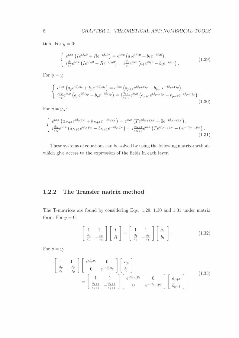
where f(z) is analytic on and within the contour of integration C. g(z) at the
singularity z = z0 is non-analytic. It is possible to demonstrate that the integral
over any closed path around z = z0 gives the same result. We can also consider a
path C0 which is a circle of radius r centred on the point z0 as illustrated in Fig.
1.4a.
In polar coordinates, z − z0 = reiθ and dz = ireiθdθ. The integral is thus:
∫
C0
f(z)
z − z0dz = if(z0)
∫
dθ = 2πif(z0). (1.50)
Theorem [67]: Cauchy’s integral formula Let f(z) be analytic inside and
on a simple closed contour C. Then at any point z inside the contour,
f(z) =1
2πi
∮
C
f(z′
)
z′ − zdz
′
. (1.51)
To accommodate expansions about singular point, we have to consider the
Laurent expansions that are more general expansions than Taylor series. For an
analytic function f(z) in an annular region, we consider Cauchy’s formula for the
contour shown in Fig 1.4b with C2 defined as the counter-clockwise path around
the circle. We take the limit that the segments which join the two circles come

14 CHAPTER 1. THEORETICAL AND NUMERICAL TOOLS
arbitrarily close together, so that their contributions cancel. Cauchy’s formula
then becomes:
f(z) =1
2πi
∫
C1
f(z′
)
z′ − zdz
′ − 1
2πi
∫
C2
f(z′
)
z′ − zdz
′
. (1.52)
We can write z′−z = (z
′−z0)−(z−z0). However, on the curve C1, |z′−z0| > |z−z0|,while for C2, |z′−z0| < |z−z0|. In the first integral, we pull out the term 1/(z
′−z0)
and in the second integral we pull out the term 1/(z − z0). Then, expanding the
geometric term, we have:
f(z) =1
2πi
∞∑
n=0
(z − z0)n
∮
C1
f(z′
)
(z′ − z0)n+1dz
′
+1
2πi
∞∑
n=0
(z − z0)−n−1
∮
C2
(z′ − z0)
nf(z′
)dz′
.
(1.53)
The first summation looks like the usual Taylor series expansion of an analytic
function, while the second summation is singular at the point z = z0. These two
series may be combined into one, referred to as a Laurent series:
f(z) =∞∑
n=−∞
an(z − z0)n, (1.54)
where
an =1
2πi
∮
C
f(z′
)
(z′ − z0)n+1dz
′
, (1.55)
and C is now any counter-clockwise contour within the annulus.
The last step in finding an expression of the pole z0 is to consider the Residue
theorem.
1.3.2 Residue theorem
Let us consider a function which has a Laurent expansion about the point z = z0.
The integral about a circle of radius r (the closed path) centred on this point is:
∮ ∞∑
n=−∞
an(z − z0)ndz =
∞∑
n=−∞
an
∮
(z − z0)ndz. (1.56)

1.3. THE POLOLOGY THEORY 15
The evaluation of this integral is possible term by term because the series is uni-
formly convergent.
Then, it is possible to demonstrate with Cauchy’s theorem that all terms for
which n ≥ 0 vanish. For n = −m < 0,
a−m
∮
(z − z0)−m = a−m
∫ 2π
0
r−me−imθireiθdθ = ia−mr−m+1
∫ 2π
0
e−i(m−1)θdθ.
(1.57)
This integral is identically zero, except for m = 1, or n = −1 and the contour
integral about the point z = z0 reduces to:
∮
f(z)dz = 2πia−1. (1.58)
This contour integral only depends on the value a−1, which is called the residue
of the function f(z) at z = z0, which we will write as Res(z0). In the case when
the contour encloses several singular points of f(z) as in Fig. 1.5, it is possible to
demonstrate that we finally obtain:
∮
C
f(z)dz = 2πi
[
∑
i
Res(zi)
]
. (1.59)
This equation may be stated as a theorem and this theorem reduces the eval-
uation of a contour integral of the function f(z) to the algebraic determination of
the residues of the function.
Theorem: Residue theorem [67] The integral of a function f(z) which
is analytic on and within a closed contour except at a finite number of isolated
singular points is given by 2πi times the sum of the residues enclosed by the contour.
If the singularity z = z0 is a simple pole (pole of order 1), the corresponding
Laurent expansion is:
f(z) =a−1
z − z0+
∞∑
n=0
an(z − z0)n. (1.60)
Cauchy’s theorem allows to obtain:
a−1 =1
2iπ
∫
C
f(z)dz, (1.61)

16 CHAPTER 1. THEORETICAL AND NUMERICAL TOOLS
Figure 1.5: A contour which can be used to evaluate a path integral enclosing numerous isolatedsingularities.
and also:
z0a−1 =1
2iπ
∫
C
zf(z)dz. (1.62)
Then, by comparing both results, the value of the pole z0 is:
z0 =
∫
Czf(z)dz
∫
Cf(z)dz
. (1.63)
1.3.3 Branch points and cut lines
The existence of a square root in the quantity βj (Eq. 1.28) implies a problem
of definition in the complex plane. Indeed, some singularities cannot be classified
using an ordinary Laurent series. A classical example is also the square root of a
complex function:
f(z) = z1/2. (1.64)
For a real function f(x) =√x, we already have to choose between two possible
roots, +√x and −√
x. For the roots of a complex number z with z = z0e2πni, we

1.3. THE POLOLOGY THEORY 17
x
y
z=0
z=z0
(a)
x
y
z=0
z=z0
(b)
x
y
z=0
cut line
(c)
Figure 1.6: The multivalued nature of the function f(z) = z1/2 with the branch point z = 0:
(a) Starting at point z0 with f(z0) = z1/20 ; (b) Ending at point z0 with f(z0) = −z
1/20 . (c)
The cut line (where argument discontinuous) introduced by defining a multivalued function bya branch defined by 0 < arg(z) < 2π.
have the same dilemma:
z1/2 = z1/20 eπni =
+z1/2,
or
−z1/2.
(1.65)
Likewise, there are two possible choices for the square root, except at the point
z = 0, where the only possibility is 0. Then, we have the following problem: when
we consider a closed circular path around the point z = 0 and if we are starting at
the point z = z0 (Fig. 1.6a), we are ending up at a different value than when we
started,
f(z) → z1/20 eπi = −z
1/20 , (1.66)
as it is illustrated in Fig. 1.6b. It is not possible to develop a Taylor or Laurent
series for the point z = 0. This kind of point is called a branch point and the
function z1/2 has two ”branches”, a positive one and a negative one.
In this case, we always choose the positive branch of f(z) = z1/2, but one line
in the complex plane along which the function f(z) is discontinuous always exists
as illustrated in Fig 1.6c.
Such a line is usually referred to as a cut line. Fortunately, its location depends
on the phase of the complex number. If 0 ≤ arg(z) < 2π, the cut line runs from

18 CHAPTER 1. THEORETICAL AND NUMERICAL TOOLS
the origin to infinity along the positive x-axis. If −π < arg(z) ≤ π, the cut line
runs from the origin to infinity along the negative x-axis. It is possible to choose
other arguments to move the cut lines in other directions. In our case, it is often
necessary to move it because the function f(z) is non-analytic along this cut line
and Cauchy’s theorem cannot be used across this line. Therefore, we wrote a
function in Matlab in order to move it and to have access to the poles we were
looking for 4.
Riemann sheets
Another possibility, introduced by B. Riemann, is to consider both branches to-
gether. As we have noted, our choice of the location of the cut line is arbitrary
for the function f(z) = z1/2. Riemann suggested that the proper domain of the
function f(z) is a pair of complex planes which are joined together along the cut
line, as opposed to a single complex plane.
This geometry is illustrated in Fig. 1.7 and corresponds to the construction of
a surface by cutting each of the two complex planes along their cut lines, and then
connecting the cut edges of one plane to the opposing edges of the other.
Therefore, the function f(z) is analytic on this pair of complex planes except at
the point z = 0. This linked set of planes is referred to as a Riemann surface, and
each individual complex plane is called a Riemann sheet. It must be noted that
the Riemann surfaces cannot be constructed in three-dimensional space without
the surfaces crossing. If we consider the function f(z) = z1/3, we find that the
Riemann surface consists of three complex planes joined together along a cut line.
Branch points are broadly grouped into three categories. Algebraic branch
points are those of the form of a fractional power of z and can be expressed by a
series,
f(z) = (z − z0)α
∞∑
n=−∞
an (z − z0)n , (1.67)
when an = 0 for all n < −N . In such a case, the function can be described by
a finite number of Riemann sheets. If an 6= 0, as n → −∞, it is referred to as
a transcendental branch point, and it is the multivalued analogue of an isolated
4According to the location of the cut line, a pole can be seen as a zero and a zero as apole. That is why we need to know in advance where we have to look in order to find the polescorresponding to the physical modes.

1.4. THE TETRACHOTOMY METHOD 19
(a) (b)
Figure 1.7: (a) An illustration of the Riemann surfaces of the multivalued function f(z) = z1/2.(b) The real part of
√z, showing how the two surfaces are tied together.
essential singularity. Logarithmic branch points are those which behave as follows:
f(z) = (z − z0)α log (z − z0)
∞∑
n=−∞
an (z − z0)n . (1.68)
In such a case, the function can be described with an infinite number of Riemann
sheets.
The main drawback for our study is the presence of the square root in the
expression of βj (Eq. 1.28). We stay in the case of algebraic branch points and
the use of our function to move the cut line is always enough to apply Cauchy’s
theorem at the right regions. An interesting method that applies Cauchy’s theorem
to find the modes in a structure - initially in photonic crystals - was developed by
F. Zolla et al. [48]. This method is called the tetrachotomy method and we have
adapted it to our study.
1.4 The tetrachotomy method
1.4.1 Poles of a meromorphic function
The tetrachotomy method allows to find the poles in the complex plane corre-
sponding to a given meromorphic function f(α) in C [48]. If f(α) has a single
pole at α0, then in the neighbourhood of that point there exists a non-vanishing

20 CHAPTER 1. THEORETICAL AND NUMERICAL TOOLS
holomorphic function G(α) (in C\α0) and the function f can be written as [68]:
f(α) =G(α)
α− α0
. (1.69)
First, we consider a Jordan loop Γ which only contains the pole α0. We assume
that the pole α0 is simple and that G does not have a pole at α = 0, so that we
can rewrite it G(α) = αF (α) with F a holomorphic function. We can demonstrate
that the following integrals allow to determine the pole α0:
I0 =1
2iπ
∫
Γ
f(α)
αdα =
1
2iπ
∫
Γ
F (α)
α− α0
dα, (1.70)
I1 =1
2iπ
∫
Γ
f(α)dα =1
2iπ
∫
Γ
αF (α)
α− α0
dα, (1.71)
I2 =1
2iπ
∫
Γ
αf(α)dα =1
2iπ
∫
Γ
α2 F (α)
α− α0
dα. (1.72)
F being a holomorphic function, that implies the integrals∫
ΓF (α)dα and
∫
ΓαF (α)dα are vanishing. Then,
I1 =1
2iπ
∫
Γ
αF (α)
α− α0
dα =1
2iπ
∫
Γ
α0F (α)
α− α0
dα +1
2iπ
∫
Γ
F (α)dα, (1.73)
and after simplification:
I1 =α0
2iπ
∫
Γ
F (α)
α− α0
dα = α0I0. (1.74)
The expression of the pole is also α0 = I1/I0. Similarly,
I2 =1
2iπ
∫
Γ
α2 F (α)
α− α0
dα =1
2iπ
∫
Γ
αF (α)dα+α0
2iπ
∫
Γ
F (α)dα+α20
2iπ
∫
Γ
F (α)
α− α0
dα.
(1.75)
The expression of the pole is then α20 = I2/I0 = α0I1/I0.
The pole α0 of the function f(α) is precisely given by:
α0 =I2I1
=I1I0. (1.76)
This is the direct application in the case where there is only one pole. As a
1.4. THE TETRACHOTOMY METHOD 21
Γu
αR
αIΓ21
Γ
Γd
Γl
Γ2
Γ4
Γ1
Γ3
Γ22
Γ23 Γ24
Γr
Figure 1.8: The Tetrachotomy algorithm performed on a rectangle in the complex plane(αR, αI). The poles are represented by red crosses.
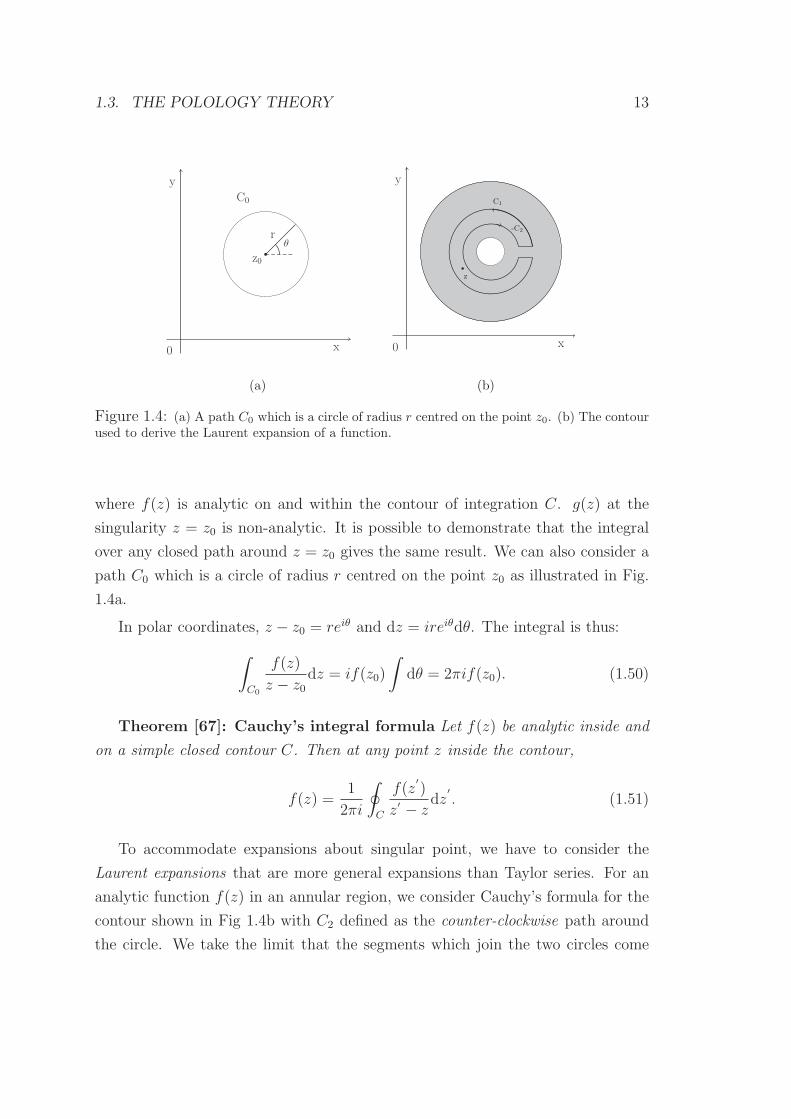
matter of fact, for a given meromorphic function f in C, the number of correspond-
ing poles αi in the complex plane is unknown. The schematic representation of
the tetrachotomy method is shown in Fig. 1.8.
The first step is then to isolate the poles from each other. The evaluation of
the integrals I0, I1 and I2 enables to know if there is no pole, one pole or several
poles inside the loop Γ. Indeed, three possibilities arise:
1. If I0 = I1 = 0, there is no pole inside the considering loop (as in the loops
Γ1, Γ4 and Γ24 in Fig. 1.8).
2. If I2/I1 6= I1/I0, that means there are several poles (as the loop Γ2 in Fig.
1.8).
3. When I2/I1 = I1/I0, there is one pole in the considering loop and the evalu-
ation of one of the fractions of Eq. 1.76 gives very precisely the sought pole
(as in the loops Γ3, Γ21, Γ22 and Γ23 in Fig. 1.8).
The principle of the tetrachotomy method is, whenever the second situation
arises, to divide the rectangle Γ into four equal rectangles Γi (i = [1, 2, 3, 4]), and
22 CHAPTER 1. THEORETICAL AND NUMERICAL TOOLS
to repeat the process until the initial rectangle is divided into rectangles which all
contain only one pole as it is illustrated in Fig. 1.8.
The efficiency of this method is linked to the numeric evaluation of the integrals
I0, I1 and I2. Their precise determination is possible because f(α) is analytic in
C \ αi. The restrictive function f to the rectangle Γ, noted f(α)|Γ, is regular as
the curve Γ and that means it is continue only. However, if we split the initial loop
as (Fig. 1.8):
∫
Γ
f(α)dα =
∫
Γd
f(α)dα +
∫
Γr
f(α)dα +
∫
Γu
f(α)dα +
∫
Γl
f(α)dα, (1.77)
the function f(α)|Γa(a = d, r, u, l) is also always derivable.
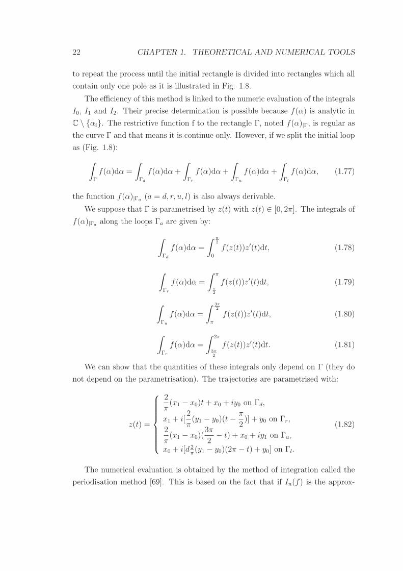
We suppose that Γ is parametrised by z(t) with z(t) ∈ [0, 2π]. The integrals of
f(α)|Γaalong the loops Γa are given by:
∫
Γd
f(α)dα =
∫ π2
0
f(z(t))z′(t)dt, (1.78)
∫
Γr
f(α)dα =
∫ π
π2
f(z(t))z′(t)dt, (1.79)
∫
Γu
f(α)dα =
∫ 3π2
π
f(z(t))z′(t)dt, (1.80)
∫
Γr
f(α)dα =
∫ 2π
3π2
f(z(t))z′(t)dt. (1.81)
We can show that the quantities of these integrals only depend on Γ (they do
not depend on the parametrisation). The trajectories are parametrised with:
z(t) =
2
π(x1 − x0)t+ x0 + iy0 on Γd,
x1 + i[2
π(y1 − y0)(t−
π
2)] + y0 on Γr,
2
π(x1 − x0)(
3π
2− t) + x0 + iy1 on Γu,
x0 + i[d 2π(y1 − y0)(2π − t) + y0] on Γl.
(1.82)
The numerical evaluation is obtained by the method of integration called the
periodisation method [69]. This is based on the fact that if In(f) is the approx-
1.4. THE TETRACHOTOMY METHOD 23
imation of I =∫ b
af(t)dt, the error yielded by the rectangle method integration
en = In − I decreases as O( 1N), where N is the number of rectangles used to ap-
proximate the function and goes to infinity [70]. However, if f is a function of
class C2k on the integration interval [a, b] and if its odd-order derivatives satisfy
the condition:
∀p ∈ 1, . . . , k − 1q(2p−1)(a) = q(2p−1)(b), (1.83)
then the error behaves like O(N−2k) when N goes to infinity, which means the
evaluation is more efficient and more precise. The functions f(z(t))z′(t) are func-
tions of class C∞([a, b]) but they are not functions that satisfy the condition Eq.
1.83.
With the periodisation method, it is possible to find a change of variables such
that the parametrisation of the integrals yields an integrand that verifies condition
Eq. 1.83. Hence, the computation of the integrals is made fast and accurate.
The change of variable is t = P (x), where P (x) is a 4k − 3-degree polynomial
given by:
P (x) =
∫ b
a(t− a)2k−2(b− t)2k−2dt
∫ x
a(t− a)2k−2(b− t)2k−2dt
. (1.84)
This polynomial is strictly increasing on [a, b] and verifies the following properties:
P (a) = 0, P (b) = 1, (1.85)
P [l](a) = P [l](b) = 0, 1 ≤ l ≤ 2k − 1. (1.86)
Thus, the integral of the function f is given by:
I =
∫ b
a
g(x)dx, (1.87)
with g(x) = P ′(x)f(P (x)) where g(x) is a function of class C2k that satisfies the
condition of Eq. 1.83.
In practice, taking k = 2 is enough. The convergence in O( 1N4 ) is sufficient
(ten times more points give four supplementary significant numbers). Thus, to
calculate the integral I, the rectangle method is applied to g(x) so as to obtain
the periodisation method.

24 CHAPTER 1. THEORETICAL AND NUMERICAL TOOLS
0 0.2 0.4 0.6 0.8 10
0.1
0.2
0.3
0.4
0.5
0.6
0.7
0.8
0.9
1
Re(α)
Im(α
)
Figure 1.9: The poles found using the tetrachotomy method for a test function (red crosses)plotted against the exact (simple) poles of the meromorphic test function (black circles).
1.4.2 Application
To test the validity of the tetrachotomy method, we consider the following function:
f(α) =g(α)
(α− αi)n, (1.88)
where f is meromorphic in C \ αi and αi are the poles of the f .
In the complex plane defined by (αR ∈ [0, 1], αI ∈ [0, 1]), we consider twenty
five poles αi randomly chosen (with the function rand of Matlab) and we apply the
algorithm to this function. The results show that the poles found by the program
are extremely close to the ones we entered as input data (see Fig. 1.9). The
corresponding randomly values are shown in Table 1.1. We also have at least eight
identical numbers which is the tolerance number we imposed in our computations.
The CPU took around 8 seconds to find these poles.

1.4. THE TETRACHOTOMY METHOD 25
Re(f) Re(αi) Im(f) Im(αi)0.120187017987081 0.120187019625525 0.419048292043586 0.4190482936248830.540884081241476 0.540884081237328 0.064187087388841 0.0641870873918990.255386740488051 0.255386740486275 0.505636617569718 0.5056366175717560.546449439903068 0.546449439902904 0.317427863654375 0.3174278636558500.020535774658185 0.020535774658272 0.635661388861370 0.6356613888613770.525045164762609 0.525045164762852 0.390762082203825 0.3907620822041750.036563018048453 0.036563018048448 0.671202185356518 0.6712021853565360.516558208351270 0.516558208351338 0.440035595760317 0.4400355957602540.702702306950475 0.702702306950754 0.257613736712109 0.2576137367124380.153590376619400 0.153590376619546 0.751946393867338 0.7519463938674500.653699889008253 0.653699889008506 0.443964155018388 0.4439641550188100.180737760254794 0.180737760254770 0.852263890343852 0.8522638903438460.325833628763249 0.325833628762824 0.816140102875546 0.8161401028753230.163512368527526 0.163512368527536 0.866749896999316 0.8667498969993190.415093386613047 0.415093386613128 0.789073514938985 0.7890735149389580.398880752383199 0.398880752383432 0.814539772900878 0.8145397729006510.932613572048564 0.932613572048764 0.060018819779211 0.0600188197794760.163569909784993 0.163569909784167 0.921097255892383 0.9210972558921970.953457069886248 0.953457069886728 0.228669482105789 0.2286694821055010.748618871776197 0.748618871774508 0.642060828437204 0.6420608284338520.679733898210467 0.679733898210444 0.767329510776502 0.7673295107765740.665987216411111 0.665987216411121 0.794657885388843 0.7946578853887530.894389375354243 0.894389375354296 0.577394196706578 0.5773941967066490.809203851293793 0.809203851294856 0.715212514781598 0.7152125147858400.923675612620407 0.923675612618613 0.950894415380493 0.950894415378135
Table 1.1: The real part Re(f) and the imaginary part Im(f) of the poles of the test function f as comparedto the calculated poles αi = Re(αi) + iIm(αi) with the tetrachotomy method. The agreement is pretty goodwith at least eight identical numbers for the real and imaginary parts, which is the tolerance number weimposed in our computations.

26 CHAPTER 1. THEORETICAL AND NUMERICAL TOOLS

Chapter 2
Coupling Surface Plasmon
Polaritons
Overview Research in plasmonics has gone made very fast progress inthe last decades [8, 9, 10, 11, 12, 13]. Since 1990, the study of plas-monic waveguides and plasmonic enhanced (extraordinary) transmission[14] has greatly boosted the exposure of the subject. Plasmonics is abranch of optical condensed matter devoted to optical phenomena at thenanoscale in structured metallic systems, due to modes called surfaceplasmon polaritons (SPPs). SPPs, predicted more than 50 years agoby R. H. Ritchie [3] and extensively studied ever since [5, 71], play keyroles in today’s nanophotonics [29]. They are optical surface waves thatpropagate (typically) along the metal-dielectric interface. But they arealso characterized by a high attenuation due to the intrinsic losses in themetal, limiting the applications [30, 31, 32, 33]. The aim of this chap-ter is to present the best known way to enhance the surface plasmonemission, which is coupling it with another surface plasmon. It is possi-ble in structures which are composed of a metallic film in a symmetricmedium. Indeed, a metallic film supports two SPP that are coupled andthe strength of this coupling depends on the metallic thickness. This cou-pling helps improve the propagation length of surface plasmons. After areminder of the basic properties of the SPP modes, we present the longrange surface plasmon polariton (LRSPP ) which corresponds to one ofthe coupled SPP in thin metallic film. It is demonstrated how to obtainthis mode on a metallic film deposited on a perfect electric conductorsubstrate. This possibility allows to not excite the short range surfaceplasmon polariton (SRSPP ) mode and to obtain the LRSPP withouta symmetric device.
27
28 CHAPTER 2. COUPLING SURFACE PLASMON POLARITONS
2.1 Surface plasmon polaritons at a single inter-
face
2.1.1 Existence conditions
In order to investigate the physical properties of SPPs, we have to begin by the
Drude model. This model gives a well known relation between metal permittivity
and plasma frequency. It was proposed by Paul Drude in 1900 [72] in order to
explain the transport properties of electrons in materials, especially in metals.
To describe the optical properties of metals, we can consider a gas made up of
free conduction electrons. This free electron gas can collectively oscillate and this
longitudinal displacement of the density of charges is called a plasmon. Its energy
quantum is ~ωp, where ωp is the plasma frequency:
ωp =
√
Nee2
ε0me
, (2.1)
where Ne is the electrons’ density, e the charge of electrons, ε0 the dielectric con-
stant of the vacuum and me the electron mass. In this work, we apply the kinetic
theory. As a consequence, the electron gas is treated as neutral solid spheres. Its
motion is uniform rectilinear until collision. The metal is also like a set of conduc-
tion electrons which are free to move with these negative charges and relatively
immobile positive ions.
The dielectric permittivity εm, which is the response of the metal to an exci-
tation with the pulsation ω is given by:
εm(ω) = 1−ω2p
ω(ω + iΓ), (2.2)
where Γ is the damping factor (it is used to account for the dissipation of the
electron motion) and ωp the plasma frequency. In the present work, we mostly
consider silver metal for computations where Γ = ωp/428 and ωp = 1.374 × 10¹⁶
s−1 [73] 1. In the case of metal without losses, the dielectric permittivity becomes
1A reason for not using gold is that, it was demonstrated for a wavelength λ < 520 nm thatthe photons do not transfer their energy to the SPs but to the individual electrons to generateintraband transitions, which cancels the SP resonance [74]. M. Watanabe et al. [75] present

2.1. SURFACE PLASMON POLARITONS AT A SINGLE INTERFACE 29
εm
(a)
y
εm
εd
x0
(b)
Figure 2.1: (a) Volume plasmon in a bulk metal with a permittivity εm. (b) Surface plasmonat the interface between a dielectric (εd) and a metal (εm).
εm(ω) = 1− ω2p/ω
2.
Two types of plasmons can be distinguished. In bulk metal (Fig. 2.1a), the
collective oscillation of the electron gas is called volume plasmon, whereas the
interface between a metal and a dielectric support is a surface plasmon (Fig. 2.1b).
Lastly, when the collective oscillation of the electron gas is coupling with light, this
mode is called a surface plasmon polariton (SPP ). In what follows, we will only
consider these SPP modes and we can use SP to simplify the notation.
SPs are surface mode solutions of Maxwell’s equations with appropriate bound-
ary conditions. We search these solutions at a flat interface between a metal and a
dielectric. It is possible to demonstrate that SPs only exist in transverse magnetic
(TM) polarization. We consider time harmonic modes with the magnetic field lin-
early polarized along a direction which is transverse to the direction of propagation
z. We denote the magnetic field asH = u(x, y)ez and the time dependence is e−iωt.
The field u(x, y) satisfies the following Helmholtz’s equation:
div(ε−1j ∇u) + k2
ju = 0, (2.3)
where k2j = k2
0εj is the wave vector in each medium (j = d,m). This equation has
to be solved separately in regions of constant εj. The solutions obtained have to
be matched using appropriate boundary conditions. We note εm for y < 0 and εd
for y > 0, the permittivities of the metal and the dielectric respectively. α and βj
this as ”anomalous reflection of gold” because below this wavelength, the gold loses its metallicproperties of reflectivity.

30 CHAPTER 2. COUPLING SURFACE PLASMON POLARITONS
(j = d,m) are the wave vectors in the x and the y directions.
We note u(x, y) = eiαxU(y) and the field U(y) satisfied the following equations:
y > 0:∂2U
∂y2+ (k2
d − α2)U = 0,
y < 0:∂2U
∂y2+ (k2
m − α2)U = 0.
(2.4)
The solutions are:
y > 0: U(y) = a1e−iβdy + b1e
iβdy,
y < 0: U(y) = a2e−iβmy + b2e
iβmy,(2.5)
where βj (j = d,m) are defined by the relation α2 + βj2= k2
0εj.
The solution corresponding to surface waves along the x direction imposes that
the field is evanescent along the y direction so that βj must be imaginary. We have
| α |> k0√εj and βj are written as:
βj = i√
α2 − k20εj. (2.6)
We note βj = iβj. However, we must impose a1 = 0 and b2 = 0 (as the modes
are bound to the surface, they must decay with increasing/decreasing y) and the
field is rewritten as:
y > 0: U(y) = b1e−βdy,
y < 0: U(y) = a2eβmy.
(2.7)
At y = 0, U and ε−1j ∂yU must be conserved in the TM polarization:
b1 = a2,
−βd
εdb1 =
βm
εma2.
(2.8)
To obtain the solution, we can solve the system of Eq. 2.8 or consider the
cancellation of the coefficient of reflection’s denominator. The result must be the

2.1. SURFACE PLASMON POLARITONS AT A SINGLE INTERFACE 31
same:βd
εd+
βm
εm= 0. (2.9)
And the corresponding dispersion relation for the SP is:
kSP = ±k0
√
εdεmεd + εm
, (2.10)
where kSP is the corresponding in-plane wave vector (propagation constant) α for
the surface plasmon.
In the case of a real metal (with losses), kSP and necessarily βm and βd are
complex, which implies a sinusoidal supplementary component (along the y direc-
tion) to the evanescent envelope of the field. We note εm = ε′
m + iε′′
m. With the
convention of signs in the exponents and to verify Eq. 2.9, the real part dielectric
permittivities ε′
m and εd must have opposite signs. Since dielectrics have a positive
(and real) εd, that means εm must be negative. In addition, the real part of the
dispersion relation (Eq. 2.10) involves a supplementary condition: the propagation
along x is only possible through the existence of a real part for kSP . These two
conditions imply ε′
m > −1 [5].
These conditions are largely fulfilled by several metals in the visible and near-
infrared ranges of the spectrum. In these ranges, εm for silver has a large negative
real part and a small positive imaginary part associated to the absorption and the
scattering losses in the metal.
2.1.2 The dispersion relation
To properly understand SP modes, we have to examine the corresponding dis-
persion relation, the relationship between the frequency ω and the in-plane wave
vector α. The in-plane wave vector is the wave vector of the mode in the plane of
the surface along which it propagates. For light in free space, the wave vector is
given by k0 = ω/c (the light line), c being the speed of light. In a medium with
the dielectric permittivity εd, the dispersion relation becomes k =√εdk0. Lastly,
for SPs propagating along the interface between a metal and a dielectric, the dis-
persion relation (Eq. 2.10) is found by looking for the surface mode solutions of
Maxwell’s equations in the section 2.1.1.
Fig. 2.2a illustrates an interface between air (εd = 1) and a metal (εm). By

32 CHAPTER 2. COUPLING SURFACE PLASMON POLARITONS
x
εd
y
εmSP
(a)
0 2
1
α c / ωp
ω / ω
p
Light line
ω
ωSP
k0 k
SP
(b)
Figure 2.2: (a) Single plane interface between a dielectric (εd = 1 ) and a metal (εm) whichsupports a SP . (b) The dispersion relation, found by taking the real part of Eq. 2.10 with themetallic permittivity based on the Drude model (Eq. 2.2) and the plasma frequency ωp for silver.The constant of propagation α is plotted in units of ωp/c and the frequency ω in units of ωp. Thelight line is the dispersion line for light in free space, k0 = ω/c. The asymptotic surface plasmonfrequency corresponds to ωSP = ωp/
√1 + εd. The dispersion curve for a SP mode shows the
momentum mismatch problem: the SP mode is always lying beyond the light line because itswave vector kSP is greater than the wave vector of a free space photon k0 at a given frequencyω. It is a non-radiative mode.
substituting the expression of εm by the dielectric permittivity of silver based on
the Drude model (Eq. 2.2), and by taking the real part of Eq. 2.10, we can plot
the corresponding dispersion relation (Fig. 2.2b).
Fig. 2.2b illustrates the dispersion curve of the SP modes. At low frequencies,
the dispersion curve lies very close to the light line, also said to be light-like. It
is a region where this mode is best described as a polariton. Then, the frequency
rises and the mode moves further away from the light line, approaching gradually
an asymptotic limit, the surface plasmon resonant frequency ωSP = ωp/√1 + εd
which translates in term of frequencies the condition ε′
m > −1. This occurs when
the permittivity of the metal and of the dielectric are of the same magnitude (but
opposite sign), which is producing a pole in the dispersion relation.
By definition, for propagating waves (PW ), kPW < k0 = ω/c (these waves have
a dispersion relation above the light line) when for SP modes, kSP > k0. The wave
vector corresponding to SP mode is always higher than the light line. We also
say that the SP is a non-radiative mode. This is the evanescent behavior of these
surface modes that forbids a direct excitation with a propagating electromagnetic

2.1. SURFACE PLASMON POLARITONS AT A SINGLE INTERFACE 33
wave. A photon and a SP at the same energy level, never have the same quantity
of motion.
There are two distinct ways to excite SP modes: with high energy electrons [76]
or with electromagnetic waves. We will only consider the use of electromagnetic
waves. In this case, classical techniques used to excite SP modes employ diffraction
by gratings or attenuated total reflection (ATR). In this work, we will consider SPs
supported by silver films and excited by electromagnetic waves using the ATR in
the Kretschmann configuration [5], which will be presented in section 2.3.1.
2.1.3 SP length scales
The first important length characterizing the SP is its wavelength λSP , which
corresponds to the period of the surface charge density oscillation and the field
distribution of the mode. The wavelength λSP comes from the real part of the
complex dispersion relation k′
SP (Eq. 2.10):
λSP =2π
k′
SP
= λ0
√
εd + ε′
m
εdε′
m
, (2.11)
where λ0 is the free space wavelength.
This SP wavelength is very similar, but always less than the free space wave-
length λ0. The fact that λSP < λ0 is a consequence of the bound nature of the SP
modes.
The propagation length
The propagation length δSP of the SP mode corresponds to the extension in the
x-direction of the field along the surface [77, 78, 79]. It is defined by the distance
over which the intensity of the mode decreases to 1/e of its initial value [80]. It is
given by δSP = 1/2k′′
SP . The imaginary part k′′
SP is:
k′′
SP = k0ε′′
m
2(ε′
m)2
(
ε′
mεdε′
m + εd
)
3
2
. (2.12)
So then:
δSP = λ0(ε
′
m)2
2πε′′
m
(
ε′
m + εdε′
mεd
)
3
2
. (2.13)

34 CHAPTER 2. COUPLING SURFACE PLASMON POLARITONS
400 600 800 1000 1200 1400 16000
50
100
150
200
250
300
λ (nm)
δS
P (
µm
)
Figure 2.3: The SP propagation length δSP as a function of the free space wavelength λ whichvaries from visible to near-infrared range. The metal considered is silver, based on the Palik data[81] and the dielectric is air, εd = 1.
The SP propagation length δSP as a function of the free space wavelength is
plotted in Fig. 2.3. The dielectric permittivity of the metal εm is taken from the
Palik data set [81] (experimental data) for silver. This choice will be justified in
Section 2.2. The increase of the propagation length is explained by the fact that for
longer wavelengths, the metal becomes a better conductor. The SP wave vector is
closer to the free space wave vector and, as it is shown with the dispersion curve,
the mode is thus light-like. Consequently, the mode is less confined to the surface.
Furthermore, it is possible to approximate the propagation length when using
low loss metal and when the condition | ε′
m |> εd is satisfied:
δSP ≈ λ0(ε
′
m)2
2πε′′
m
. (2.14)
With this approximation, we can see that to have a much higher propagation
length δSP , we need a large (negative) real part ε′
m and a small imaginary part ε′′
m.
In the visible and near-infrared ranges, silver respects these properties.
The penetration depths
By definition, the penetration depths of a surface mode correspond to the spatial
(vertical) extension of its field in both media in the y-direction [82]. For a material
with a dielectric permittivity εi (i = d,m), it is possible to express the total wave
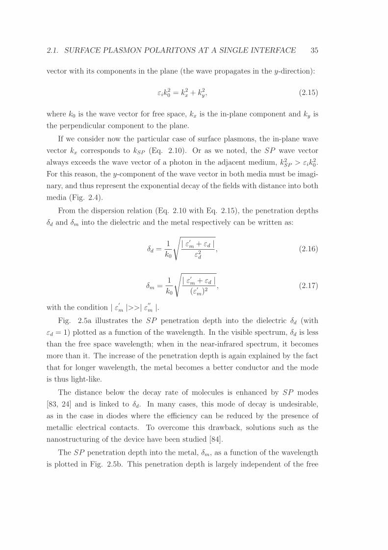
2.1. SURFACE PLASMON POLARITONS AT A SINGLE INTERFACE 35
vector with its components in the plane (the wave propagates in the y-direction):
εik20 = k2
x + k2y, (2.15)
where k0 is the wave vector for free space, kx is the in-plane component and ky is
the perpendicular component to the plane.
If we consider now the particular case of surface plasmons, the in-plane wave
vector kx corresponds to kSP (Eq. 2.10). Or as we noted, the SP wave vector
always exceeds the wave vector of a photon in the adjacent medium, k2SP > εik
20.
For this reason, the y-component of the wave vector in both media must be imagi-
nary, and thus represent the exponential decay of the fields with distance into both
media (Fig. 2.4).
From the dispersion relation (Eq. 2.10 with Eq. 2.15), the penetration depths
δd and δm into the dielectric and the metal respectively can be written as:
δd =1
k0
√
| ε′
m + εd |ε2d
, (2.16)
δm =1
k0
√
| ε′
m + εd |(ε′
m)2
, (2.17)
with the condition | ε′
m |>>| ε′′
m |.Fig. 2.5a illustrates the SP penetration depth into the dielectric δd (with
εd = 1) plotted as a function of the wavelength. In the visible spectrum, δd is less
than the free space wavelength; when in the near-infrared spectrum, it becomes
more than it. The increase of the penetration depth is again explained by the fact
that for longer wavelength, the metal becomes a better conductor and the mode
is thus light-like.
The distance below the decay rate of molecules is enhanced by SP modes
[83, 24] and is linked to δd. In many cases, this mode of decay is undesirable,
as in the case in diodes where the efficiency can be reduced by the presence of
metallic electrical contacts. To overcome this drawback, solutions such as the
nanostructuring of the device have been studied [84].
The SP penetration depth into the metal, δm, as a function of the wavelength
is plotted in Fig. 2.5b. This penetration depth is largely independent of the free

36 CHAPTER 2. COUPLING SURFACE PLASMON POLARITONS
δm
δd
y
| Ey |
Figure 2.4: The field in the perpendicular direction is evanescent, reflecting the bound, non-radiative nature of SPs. This prevents power from propagating away from the surface. In thedielectric medium (typically air or glass), the penetration depth is δd, whereas the penetrationlength into the metal is δm.
400 600 800 1000 1200 1400 16000
500
1000
1500
2000
2500
3000
λ (nm)
δd (
nm
)
(a)
400 600 800 1000 1200 1400 160022
23
24
25
26
27
28
29
λ (nm)
δm
(nm
)
(b)
Figure 2.5: The SP penetration depths as a function of the free space wavelength λ whichvaries from visible to near-infrared range. The metal considered is silver, based on the Palik data[81] and the dielectric is air, εd = 1. (a) The SP penetration depth into the dielectric δd. (b)The SP penetration depth into the metal δd.

2.2. DIELECTRIC PERMITTIVITY OF METALS 37
500 1000 1500 2000−250
−200
−150
−100
−50
0
50
λ (nm)
ε’ m
Drude model
Palik data
JC data
(a)
500 1000 1500 2000
0
5
10
15
20
25
30
λ (nm)
ε’’ m
Drude model
Palik data
JC data
(b)
Figure 2.6: The real (a) and imaginary (b) parts of the silver dielectric permittivity εm(ω) =ε′
m(ω)+ε′′
m(ω) using the Drude model (gray dashed line), the Palik data [81] (black line) and theJohnson and Christy data [85] (red line). A zoom is made on the region of wavelengths between200 nm and 600 nm.
space wavelength in this wavelength range. Indeed, in this range ω << ωp and we
can approximate δm as:
δm =λp
2π, (2.18)
where λp is the wavelength corresponding to the plasma frequency ωp. For silver,
ωp = 1.374×10¹⁶ s−1 and the penetration depth in the metal is δm = 22 nm, which
is not so far from the average value in Fig. 2.5b. Note that the penetration depth
rises for short wavelengths because the condition ω << ωp is no longer valid.
The parameter δm represents the necessary thickness for the metallic films that
allows the coupling of a SP mode, as with propagating light in the prism coupling
configuration (Kretschmann) or with another SP modes in a metallic thin film
device.
2.2 Dielectric permittivity of metals
The Drude model presented in Section 2.1.1 allows to obtain the main properties
of surface plasmons. However, it gives only an approximation of the dielectric
permittivity of metals, and its validity is limited to near-infrared frequencies. We
are going to compare it to experimentally determined dielectric permittivity of
silver, as adopted from Johnson and Christy [85] and Palik [81] data sets.

38 CHAPTER 2. COUPLING SURFACE PLASMON POLARITONS
0 1.20
1.2
α c / ωp
ω /
ωp
JC data
Palik data
Light line
ωSP
ωR
Figure 2.7: Dispersion relation of SP mode on the Ag/air interface with respectively thepermittivities εm and εd = 1. The metal permittivity εm is determined from the Palik (blackline) and the Johnson and Christy (red line) data sets. For frequencies below ωSP = ωp/
√1 + εd,
the typical bound SP mode is observed below the light line plotted in dashed line (as in Fig. 2.2b).Above the asymptote at ωR, there is the radiative plasmon polariton (RPP) mode. Between thesetwo asymptotes, it is the plasmon bandgap where the plasmon wave vector is purely imaginaryand the modes in this regime (called quasibound modes) are forbidden [86].
Fig. 2.6 shows the dielectric permittivity εm(ω) = ε′
m(ω) + iε′′
m(ω) of silver as
derived from the Johnson and Christy (JC) data, the Palik data and the Drude
model (Eq. 2.2). The JC and Palik data sets are in agreement for wavelengths
between 200 nm and 600 nm. At greater wavelengths, ε′
m from JC data falls off
faster and ε′′
m grows more slowly than the corresponding results from the Palik
data. With this difference, we have to compare the results of both data sets on a
practical case, the dispersion relation of SP .
The dispersion curve of a SP supported at the interface between air (εd = 1)
and a metal (εm) is presented in Fig. 2.7, both for the JC and the Palik data sets.
As there are experimental results, the asymptote at ωSP = ωp/√1 + εd (defined
by the wavelength where ε′
m = −εd) does not go to infinity. Note here that ωp
is not well defined with its asymptote, an uncertainty still exists. For frequencies
below this asymptote, the typical bound SP mode is observed (as in Fig. 2.2b).
Above the asymptote at ωR, there is the radiative plasmon polariton (RPP) mode.
Between these two asymptotes, we have the plasmon bandgap where the plasmon
wave vector is purely imaginary and the modes in this regime (called quasibound

2.3. METALLIC FILM IN NON-SYMMETRIC MEDIUM 39
modes) are forbidden [86]. The agreement between the two curves from JC and
Palik data sets is satisfactory. We also chose to use the Palik data on silver in all
computations unless otherwise specified.
2.3 Metallic film in non-symmetric medium
In this section, we will describe the properties of the surface plasmons supported
by a metallic film in a non-symmetric medium. It is the most commonly used
configuration to excite and exploit SPs. To begin, the optical methods used to
excite them shall be detailed. Afterwards, two well known figures of merit of the
surface plasmons will be presented: the characterized dip of reflectivity on the
metallic surface for a specific angle of incidence; and the map of the magnetic field
corresponding to the surface plasmon (in the transmitted medium).
2.3.1 Optical coupling of SPs
As we saw in the first section, SP modes are non-radiative modes. To couple
these modes with light waves, special devices must to be employed [87]. Indeed,
the coupling can be achieved using a coupling medium, such as a grating or a
prism, to match the photon and surface plasmon wave vectors. A grating coupler
matches the wave vectors by increasing the parallel wave vector component by
an amount related to the grating period. A prism can be positioned very close
to a metal surface in the Otto configuration or against a thin metallic film in
the Kretschmann configuration. We will give more precisions for both of these
methods.
Metallic gratings
Metallic gratings can be used to satisfy the energy and momentum matching con-
ditions of the wave vectors. We consider an incident wave vector ki = k0√εi with
kxi its in-plane component and θi the incident angle of this wave. We recall that
to excite a plasmon, we have to satisfy the condition:
kxi = kSP (ω). (2.19)

40 CHAPTER 2. COUPLING SURFACE PLASMON POLARITONS
θi
θd
Figure 2.8: A metallic grating constituted by a periodic structure with a period Λ.
However, kxi = ω/c sin θi < ω/c and ω/c <| kSP (ω) |. A possibility for obtaining
the equality 2.19 is to use the grating coupling [5].
A grating is a periodically corrugated surface modulation. It can be character-
ized by its periodicity or grating constant Λ. The periodic corrugation breaks the
translational invariance of the metal surface. An incident plane wave can interact
with the grating grooves, acting as an array of scattering centres. The total field
can be generated from the constructive interference of the individual scattered
waves, resulting in different diffraction orders. We consider a grating constituted
by a periodic structure with a period Λ (Fig. 2.8). The wave vectors are equal
modulo 2π/Λ (as a consequence of the Bloch theorem) and we can write:
k0 sin θd = k0 sin θi + p2π
Λ, (2.20)
where k0 = ω/c and p is a relative integer and represents the order of diffraction.
It is always possible to find an order p where:
kSP (ω) = kxi + p
2π
Λ. (2.21)
It becomes possible to excite a SP with an incident electromagnetic plane wave.
In this configuration, we have a total absorption: for a given frequency ω, we can
find an incident angle θi which respects the condition 2.21 and the corresponding
wave vector kxi = ω/c sin θi can match with kSP . It is this method that was
used in the first - accidental - observation of the SPs, and that is reported in [2] as
Wood’s anomalies. Indeed, in 1902, R. W. Wood observed sudden variations of the
intensity in the light beam spectrum, reflected by a diffraction grating in the TM

2.3. METALLIC FILM IN NON-SYMMETRIC MEDIUM 41
polarization. The intensity of the incident beam being continuous, the spectrum
had to be continuous too. These variations are due to the coupling between the
propagating incident waves and the SP waves. Following this, gratings have been
much studied by A. Hessel and A. A. Oliner [88], and more precisions are given by
R. Petit [89] and H. Raether [5].
It is also possible to excite the SP mode with a high refractive index prism, as
we are going to present.
Otto configuration
Two configurations are possible to excite SPs optically by employing a high re-
fractive index prism. In the Otto configuration [5] (Fig. 2.9a), an incident beam
is reflected on the base of a prism of high refractive index material (εd > 1). Near
to the base, there is a gap of low refractive index material (we take εa = 1), with a
thickness on the order of the incident beam wavelength [5, 90]. On the other side
of the gap, there is a metallic film (εm). The ATR takes place when the incident
angle θi is equal to, or larger than, the critical angle and creates an evanescent
field. In the prism with a permittivity εd (we take glass, εd = 2.25), the in-plane
component of the incident wave vector is kxi =
√εd sin θi. It can be higher than k0
because εd > εa. In these conditions, the incident wave can excite the SP modes
on the air/metal interface. We plot the reflectivity as a function of the incident
angle θi (Fig. 2.9b), and the coupling condition appears as a minimum of the
reflectivity for θi = 43.7. This dip of the reflectivity represents the excitation on
the SP mode.
This excitation is very sensitive to changes in the gap between the dielectric
prism and the metallic film, which explains why the method is rather unused today.
Kretschmann configuration
The Kretschmann configuration [5] is the most commonly used method to couple
light to surface plasmons because of its relative simplicity and robustness. As
illustrated in Fig. 2.10a, an incident beam is reflected on the base of a high
refractive index prism (εd > 1). A thin metallic film is located on the prism base.
The thickness of the metal layer needs to be precisely controlled in order to obtain
the most efficient coupling. Again, there is an ATR when the incident angle θi is

42 CHAPTER 2. COUPLING SURFACE PLASMON POLARITONS
ksp
glass
air
θ
metal
(a)
0 20 40 60 800
0.2
0.4
0.6
0.8
1
θi (°)
R (
I refl / I
inc)
(b)
Figure 2.9: (a) Prism coupling in the Otto configuration with the permittivities εd = 2.25(glass), εa = 1 (air) and εm (metal), taken from the Palik data [81] for silver. (b) The reflectivityis plotted as a function of the incident angle θi, with a wavelength λ = 632.8 nm. The minimumof reflectivity occurs for an angle θi = 43.7, and corresponds to the excitation of the SP whenthe thickness of the spacer is on the order of the incident wavelength.
equal to, or larger than, the critical angle and creates an evanescent field.
The in-plane component of the incident wave vector kxi can be higher than k0.
In Fig. 2.10b, reflectivity is plotted as a function of the incident angle θi. Three
cases are distinguished. The first extreme case, when there is no metallic film
(in red), represent the total internal reflection of the field between the media with
εd = 2.25 and εa = 1. The second case (in blue) corresponds to the situation where
the metallic film is too thick (as a metallic bulk). The layer becomes opaque to the
electromagnetic field and the system is like a mirror. The corresponding reflection
is still high, but lower than 1 because of the metal absorption. Finally, when the
metallic film thickness is em = 45 nm for λ = 632.8 nm, the coupling of the SP
mode occurs for an angle θi = 43.7C.
The choice of the metallic film thickness occurs from the plot of the minimum
reflectivity obtained as a function of the metallic thickness em (Fig. 2.12). The
minimum occurs for em = 45 nm.
So, it is possible to match the propagating wave vector kxi with the wave vec-
tor kSP corresponding to the interface metal/air (Fig. 2.11). The propagating
electromagnetic wave in the dielectric is also able to excite SP modes which prop-
agate in the air. An important point here is that a metallic film supports two
plasmons. In the present case, there is a plasmon at the metal/air interface and

2.3. METALLIC FILM IN NON-SYMMETRIC MEDIUM 43
ksp
glass
air
θ
metal
(a)
0 20 40 60 800
0.2
0.4
0.6
0.8
1
θi (°)
R (
I refl / I
inc)
45 nm silver film
no silver
bulk silver
(b)
Figure 2.10: (a) Prism coupling in the Kretschmann configuration with the permittivitiesεd = 2.25 (glass), εa = 1 (air) and εm (metal), taken from the Palik data [81] for silver. (b)Reflectivity plotted as a function of the incident angle θi with a wavelength λ = 632.8 nm. Theminimum of reflectivity occurs for an angle θi = 43.7 and corresponds to the excitation of theSP when em = 45 nm. The red curve represents the case where there is no metallic film, theincident beam is reflected on the base of the prism towards the air. Because εd > εa, that is theclassical case of total internal reflection. The blue curve represents the case where the metallicfilm is as a metal bulk. The system becomes like a mirror and it is impossible to excite the SPmode.
0 2
1
α c / ωp
ω /
ωp
ω = k0 sqrt(ε
d) cω = k
0 c
coupling
Figure 2.11: For light wave in vacuum, ω = k0c, when in dielectric medium (εd > 1), ω =k0√εdc = kxi c. The in-plane component of the incident wave vector can be higher than k0. There
is a frequency for which kxi = kSP and the coupling between light wave and the SP mode, whichexists at the interface metal/air becomes possible.
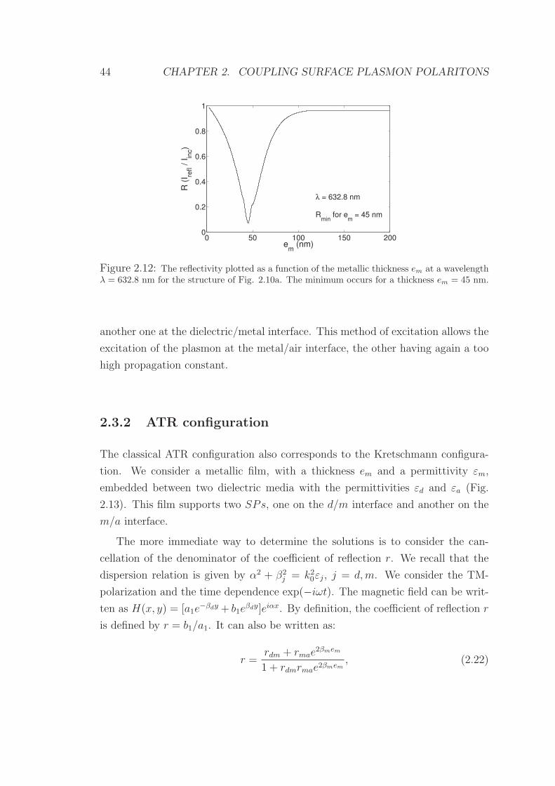
44 CHAPTER 2. COUPLING SURFACE PLASMON POLARITONS
0 50 100 150 2000
0.2
0.4
0.6
0.8
1
em
(nm)
R (
I refl /
Iin
c)
λ = 632.8 nm
Rmin
for em
= 45 nm
Figure 2.12: The reflectivity plotted as a function of the metallic thickness em at a wavelengthλ = 632.8 nm for the structure of Fig. 2.10a. The minimum occurs for a thickness em = 45 nm.
another one at the dielectric/metal interface. This method of excitation allows the
excitation of the plasmon at the metal/air interface, the other having again a too
high propagation constant.
2.3.2 ATR configuration
The classical ATR configuration also corresponds to the Kretschmann configura-
tion. We consider a metallic film, with a thickness em and a permittivity εm,
embedded between two dielectric media with the permittivities εd and εa (Fig.
2.13). This film supports two SPs, one on the d/m interface and another on the
m/a interface.
The more immediate way to determine the solutions is to consider the can-
cellation of the denominator of the coefficient of reflection r. We recall that the
dispersion relation is given by α2 + β2j = k2
0εj, j = d,m. We consider the TM-
polarization and the time dependence exp(−iωt). The magnetic field can be writ-
ten as H(x, y) = [a1e−βdy + b1e
βdy]eiαx. By definition, the coefficient of reflection r
is defined by r = b1/a1. It can also be written as:
r =rdm + rmae
2βmem
1 + rdmrmae2βmem, (2.22)

2.3. METALLIC FILM IN NON-SYMMETRIC MEDIUM 45
em
x
εa
0
y
εm
εd
Figure 2.13: Silver film with a thickness em and a permittivity εm embedded between twodielectric media with the permittivities εd and εa. For computations, εd = 2.25, εa = 1, εm istaken from the Palik data [81], em = 45 nm and the incident wavelength is λ = 632.8 nm.
where:
rdm =
βd
εd− βm
εmβd
εd+ βm
εm
and rma =
βm
εm− βa
εaβm
εm+ βa
εa
. (2.23)
A mode in this structure is defined by the existence of an outgoing field in
absence of excitation. That means b1 6= 0, a1 = 0 and corresponds to the equation
1 + rdmrmae2βmem = 0 :
(
βd
εd+
βm
εm
)(
βm
εm+
βa
εa
)
+
(
βd
εd− βm
εm
)(
βm
εm− βa
εa
)
e2βmem = 0. (2.24)
In the case of a thick metallic film, the term of propagation becomes negligible,
| exp(2βmem) | << 1 and Eq. 2.24 is simplified:
(
βd
εd+
βm
εm
)(
βm
εm+
βa
εa
)
= 0. (2.25)
Eq. 2.25 admits two solutions which correspond to SPs propagating without
coupling along the d/m and m/a interfaces as the solution given by Eq. 2.9.
We consider now the case of a thin metallic film which corresponds to the
Kretschmann configuration (section 2.3.1). In this case, εd > εa, and the metallic
thickness is em = 45 nm for an incident beam with a wavelength λ = 632.8 nm
(Fig 2.13). The modes propagating along each interface have different velocity and

46 CHAPTER 2. COUPLING SURFACE PLASMON POLARITONS
(a) (b)
Figure 2.14: (a) Map of the magnetic field in the structure corresponding to the Kretschmannconfiguration (Fig. 2.13) with εd = 2.25, εa = 1 and εm is taken from the Palik data [81] forsilver. (b) Precise map of the transmitted magnetic field: the SP mode is excited and we cansee its propagation length, as well as the exponential decay of the field in the air.
decay rates. An incident beam in the dielectric, with the angle θi = 43.7, allows
the excitation of the surface plasmon in the air (Fig. 2.14a).
In Fig. 2.14b, the SP mode is very visible with its propagation length and the
exponential decay of the field in the air. From Eq. 2.3, the propagation length
is δSP ≃ 21µm, and the corresponding propagation length from the map of the
magnetic field is δSP ≃ 14µm (see Fig. 2.14b). The calculated penetration depth
(Eqs. 2.5a and 2.5b) are δair = 388 nm and δm = 24.5 nm, which are in agreement
with the magnetic field map.
2.4 Metallic film in symmetric media
In this section, we will consider the case of a metallic film in a symmetric medium.
For thin metallic film, the properties of the two coupled SP modes supported by
the structure are presented. The involvement of the long range SP (LRSP ) is
explained through a review about it and the comparison between the length scales
of this mode and the classical SP mode is made.

2.4. METALLIC FILM IN SYMMETRIC MEDIA 47
2.4.1 The dispersion relations
One way to extend the length scale of SP modes is to make use of the coupled
SP modes supported by symmetrically thin metallic films [36]. When the metal
is thin enough, the SP modes associated to the two metal surfaces may interact
and form two coupled SP modes.
For a metallic film in a symmetric medium, εd = εa and Eq. 2.24 is simplified
as:(
βm
εm+
βd
εd
)
±(
βm
εm− βd
εd
)
eβmem = 0. (2.26)
There are two solutions for guiding modes by the metallic film depending on
the sign ”± ” in Eq. 2.26. These solutions correspond to the dispersion relations:
ω+: βdεm + βmεd tanh
(
βmem2
)
= 0, (2.27)
ω−: βdεm + βmεd coth
(
βmem2
)
= 0. (2.28)
In a symmetric medium, the SP frequency is the same on both sides of the
metallic film, so that in the case of a thin film (below 50 nm [91]) the electromag-
netic fields of both surfaces interact and the frequency splits into a low-frequency
ω− and a high frequency ω+. The splitting is associated with asymmetric (ω−)
and symmetric (ω+) electric field Ey distributions, as compared to the symmetry
of the structure. For ω−, the electric field is not cancelled in the metal, which
increases absorption due to the losses in the metal. It attenuates rapidly during
the propagation (Fig. 2.15a). This asymmetric mode is also called the short range
surface plasmon polariton (SRSP ). For ω+, the electric field is cancelled in the
metal, and the mode has a long propagation length as compared to the SP mode
supported by a bulk metallic surface. Indeed, the electric field of these modes has
a bigger depth penetration in the dielectric, and the losses by absorption in the
metal decrease (Fig. 2.15b). This symmetric surface plasmon mode is called a
long range surface plasmon polariton (LRSP ).
There is a compromise between the propagation length and the penetration
depth in a symmetric structure. It is possible to obtain high propagation length in
comparison to the case of the single interface but at the expense of the penetration
depth. The LRSP mode that propagates very far will not still remain, a surface

48 CHAPTER 2. COUPLING SURFACE PLASMON POLARITONS
emx
εd
yEy
εm
εd
(a)
x
εd
y
εm
εd
Ey
em
(b)
Figure 2.15: (a) Symmetric electric field Ey corresponding to the LRSP . (b) Asymmetricelectric field Ey corresponding to the SRSP .
mode if the the metallic film becomes too thin.
Fig. 2.16a represents the dispersion curves ω+ and ω− of the LRSP and
the SRSP modes, respectively. These dispersion curves are obtained with the
tetrachotomy method (see Chapter 1) for which the real part of the poles is noted
α and corresponds to the propagation constant of the modes. Solutions for Eq.
2.26 are found for a silver film embedded in air. Palik data for silver is used for
the metal. In the same conditions, the reflectivity is plotted as a function of the
incident angle θi (Fig. 2.16b). The half-width of the mode ω+ is smaller than the
half-width of the mode ω−. Thus, the absorption of the LRSP mode is smaller
than that of the SRSP mode.
2.4.2 Review on LRSPs
In a symmetric structure, the most interesting surface mode supported by a metal-
lic film in a symmetric media is the LRSP mode because of its low absorption in
comparison to the SRSP mode.
The first theoretical study on the existence of the LRSPs was done in the 1960s
[92]. This prediction was then confirmed by electron-loss spectroscopy in the same
decade. It was noticed that the damping of the ω+ mode slightly decreased with
a smaller thickness of the metallic film [93, 94, 95, 96, 97, 98, 34, 35]. We justify
further on our choice of metallic thickness. In the 1980s, Sarid [37] confirmed and

2.4. METALLIC FILM IN SYMMETRIC MEDIA 49
0 0.1 0.2 0.3 0.4 0.50.2
0.4
0.6
0.8
1
ω / ω
p
αR
( nm−1
)
ω+
ω−
(a)
0 20 40 60 800
0.2
0.4
0.6
0.8
1
θI (°)
R (
I refl / I
inc)
ω+
ω−
(b)
Figure 2.16: (a) Dispersion curves ω+ and ω− of the LRSP and the SRSP modes, respectively.εd = 1 is the permittivity of vacuum and the permittivity of the metal εm is taken from theexperimental data of Palik [81]. The metallic thickness is em = 30 nm. (b) In the same conditions,the reflectivity is plotted as a function of the incident angle θi. The half-width of the mode ω+ issmaller than the half-width of the mode ω−. Thus, the absorption of the LRSP mode is smallerthan that of the SRSP mode.
established the main characteristics of LRSPs as a measure of the propagation
length of these modes, twenty-seven higher than the propagation length of a surface
plasmon at the surface of a bulk metal [99, 100].
These plasmonic guides, despite the good propagation length (it can be mea-
sured in centimetres), are not interesting for optic guiding [101, 102, 103]. Indeed,
the confinement is only in one dimension (perpendicular to the interfaces), which is
a limitation for integrating these guides into electronic components. A possibility
for using it would be to reduce the width of the metallic films [36].
Up until 2009, a large bibliography on LRSPs was produced by P. Berini
[36]. In the study of LRSPs, many methods have been employed, either based
on Fresnel’s coefficients [5], on Maxwell’s equations with appropriate boundary
conditions [91] or on the method of lines [104, 105]. The method we used to find
the dispersion curves as in Fig. 2.16a, and to determine characteristic properties of
our structures consists in finding the poles of the scattering matrix. This method
is described in Chapter 1 as the tetrachotomy method.
The large range of recent applications [38, 106, 107, 108, 39, 40], such as in
photonic crystals, stratified media, quantum systems or with anisotropy, appeal to
us with respect to finding a way to excite LRSP without the short mode, and are

50 CHAPTER 2. COUPLING SURFACE PLASMON POLARITONS
δSP = 1/2Im(kSP ) Map of the magnetic field Tetrachotomy algorithmSPATR 21µm 14µm 25µm
LRSPem1=30nm 262µmLRSPem2=20nm 8.2mm
Table 2.1: Compared propagation lengths between a SP mode in the ATR configuration and the LRSP fortwo thicknesses em1 = 30 nm and em2 = 20 nm. The results tabulated here are obtained from the theoreticalexpression of the propagation length, the map of the magnetic field and the tetrachotomy algorithm. Theorder of size is correct.
experimentally feasible.
We theoretically demonstrate the equivalence between a metallic film embedded
into a symmetric medium of thickness em, and a metallic film of thickness em/2
deposited on a perfect electric conductor substrate (PECS). The interesting point
of this device is that it only supports a LRSP and is less complicated to realize
experimentally.
2.4.3 Comparison of the length scales
Table 2.1 shows the compared propagation lengths for a SP in the ATR configu-
ration and a LRSP with two metallic thicknesses em1 = 30 nm and em2 = 20 nm.
The SPATR results are determined with λ = 632.8 nm, em = 45 nm, εd = 2.25 and
εa = 1 (Fig. 2.13). The propagation length from the magnetic field map is slightly
smaller than the calculated one, which in turn is shorter than the one from the
tetrachotomy algorithm. The order of size is correct and the agreement is correct
[79].
The propagation lengths for the LRSP mode are determined with the tetra-
chotomy algorithm. They are truly higher than in the case of a single SP mode.
It is for this reason that the study of this mode is interesting for many different
applications.
2.5 Theoretical LRSP on PECS
In this section, we demonstrate the equivalence between a LRSP mode in a sym-
metric structure and the guided mode which exists on a metallic layer deposited
on a perfect electric conductor (PEC) substrate [109]. First, we consider the image

2.5. THEORETICAL LRSP ON PECS 51
charge theory and adapt it to our configuration. Then, we present the theoretical
equivalence with the compared dispersion relations of the classical LRSP and the
guided mode excited on a metallic film deposited on a PEC substrate. In perspec-
tive, we present that it would be possible to realize this device experimentally in
the terahertz (THz) frequency range.
2.5.1 Reviewed image charge theory
The image charge theory is a problem of boundary conditions [110]. We consider
a charge +q localized at a distance y = d from a perfect electric conducting plane
(Fig. 2.17a). The boundary conditions imply that the tangential components of
the electric field have vanished on the surface of the PEC. The classical illustra-
tion of this theory uses the electrostatic dipole, where a charge −q is localized
symmetrically on the other side of the plane, at a distance y = −d. The field
lines observed in the half-space containing the charge +q correspond to the field
lines of an electrical dipole, with a dipolar moment 2dq. Fig. 2.17b illustrates the
equivalent system.
That is the image charge theory that implies the equivalence between the two
configuration. In practice, the charge +q attracts the free electrons, and a density
of non-uniform surface negative charge is induced at the surface of the PEC [111].
The normal component of the field, created by the positive charge at a point P ,
located on the PEC plane at a distance r from the origin (see Fig. 2.17a), can be
written as:~Enq+
(P ) = ~Enq+(r) = − 1
4πε0
dq
(d2 + r2)3/2~ez. (2.29)
The field created by the negative charge at the point P , which cancels the
tangential components on the surface of the PEC, is given by:
~Enq−(P ) = ~Enq−
(r) = − 1
4πε0
dq
(d2 + r2)3/2~ez. (2.30)
The surface charge density at P is also:
σS(P ) = σS(r) = ε0E(r) = ε0(Enq+(r) + Enq−
(r)) = − 1
4π
2dq
(d2 + r2)3/2. (2.31)
The integration of the last expression for the charge on the surface is equal to

52 CHAPTER 2. COUPLING SURFACE PLASMON POLARITONS
(a) (b)
Figure 2.17: (a) Field lines created by an electric charge +q near a PEC substrate. (b) Fieldlines created by on electric dipole with a dipolar moment 2dq.
−q. Indeed, the conducting plane is an asymmetric plane for charges. A fictitious
charge on the other side of the plane is created at a same distance from the surface,
d. This result can be generalized to an object with an assembly of charges +q. If
that distribution of charges is placed at a distance y = d/2 from the conducting
plane, an equal and opposite distribution of charges exists at y = −d/2. With
these fictitious charges, the system becomes equivalent to a dipole with a dipolar
moment dq.
This theory can be extend to our configuration. In this case, a symmetric
metallic film with a thickness em has the same properties as a metallic film of
thickness em/2 deposited on a PEC substrate.
From an experimental point of view, it is difficult to deposit homogeneous
metallic film of less than 15 nm thickness since metals form nanoscale islands
in the initial deposition process [112]. That is why we will consider a metallic
layer of thickness em = 30 nm in the symmetric structure to obtain the limit case
where the metallic layer of thickness em/2 = 15 nm will be deposited on a PEC
substrate. However, recent studies show new possibilities for depositing thinner
metallic layers [113] but the foremost goal is to demonstrate the equivalence by
using common devices.

2.5. THEORETICAL LRSP ON PECS 53
em
x
εd
y
εm
εd
(a)
em/2
x
εd
y
εm
PEC
(b)
Figure 2.18: (a) A metallic film embedded in a symmetric medium with a thickness em and(b) a metallic layer with a thickness em/2 deposited on a PEC substrate.
2.5.2 Equivalence of the structures
We recall that the dispersion relation corresponding to the LRSP with a metallic
thickness em is (Fig. 2.18a):
ω+: βdεm + βmεd tanh
(
βmem2
)
= 0. (2.32)
The dispersion relation corresponding to the case of a metallic film deposited
on a PEC substrate can be deduced from the expression of the field in the different
layers (in TM polarization with the time dependence e−iωt):
y ≥ d/2: Hd(x, y) = a2eiαxeβ
′
dy,
0 ≤ y ≤ d/2: Hm(x, y) = eiαx(a1eβ′
my + b1e−β
′
my),(2.33)
and the magnetic field in the PEC (y < 0) is zero. We recall that β′
d > 0.
Let’s consider the boundary conditions in the TM polarization. First, for y = 0,1εm
∂yHm = 0:
a1 = b1. (2.34)
And the magnetic fields become:
Hd(x, y) = a2eiαxeβ
′
dy,
Hm(x, y) = 2a1eiαxch(β
′
my).(2.35)

54 CHAPTER 2. COUPLING SURFACE PLASMON POLARITONS
0 0.1 0.2 0.3 0.4 0.50.2
0.4
0.6
0.8
1
ω /
ωp
α ( nm−1
)
ω+
ω−
Figure 2.19: The dispersion curve obtained in Fig. 2.16a in black points with a thicknessem = 30 nm and in red points, the dispersion curve corresponding to a metallic layer depositedon the PEC substrate with a metallic thickness em/2 = 15 nm.
Then, for y = d/2, Hm = Hd and 1εm
∂yHm = 1εd∂yHd:
−2a1β′
m
εmsh(β
′
md/2) = a2β′
d
εdeβ
′
dd/2,
2a1ch(β′
md/2) = a2eβ′
dd/2.
(2.36)
Thus, the dispersion relation is:
β′
m
εmtanh(
β′
md
2) +
β′
d
εd= 0. (2.37)
Eqs. 2.32 and 2.37 are equivalent for β′
j = βj, j = d,m.
Fig. 2.19 illustrates the comparison between the corresponding dispersion
curves. This shows the equivalence between the dispersion relation ω+ of a LRSP
(upper black-squares curve), supported by a metallic layer embedded in a symmet-
ric medium, and the dispersion relation of the SP mode supported by a metallic
layer deposited on PECS (red-squares curve).
The advantage is that it is simpler to deposit a metallic layer on a plane than
to have a perfect symmetric medium around a metallic film, especially a medium
as such air. Indeed, with this configuration, it is possible to directly excite the
LRSP in air. This permits to extend its use to the enhancement of the decay rate
of molecules, for example.
The difficulty comes from the lack of availability of a PEC in the visible range.

2.5. THEORETICAL LRSP ON PECS 55
In theory, it is possible to use supraconductors2, but an immediate solution is to
consider the THz frequency range. Indeed, in this range, a doped-semiconductor
(DSC) can have the behavior of a metal in the visible range and support a SP
mode [114, 115, 116]. Metal also has the behavior of a PEC (a very high negative
real value of permittivity) [116, 109]. This study will be the subject of a future
publication.
2At wavelength range shorter than their gap.

56 CHAPTER 2. COUPLING SURFACE PLASMON POLARITONS

Chapter 3
Coupling Dielectric Waveguides
Overview Dielectric waveguides provide simple models for the confin-
ing mechanism of waves propagating in optical devices. The coupling of
waveguides has been intensively studied, in particular with the coupled-
mode theory [49, 50, 51, 52, 53]. After a recall concerning the dielectric
slab waveguides, we present the coupled-mode theory. This theory can
be derived from the variational principle for the frequencies of the sys-
tem. When a trial solution is introduced to the electric field in a lossless
electromagnetic system such as the linear superposition of modes, the
coupled-mode theory gives the result. This theory is also presented in
TM polarization, an unpublished result in the state-of-the-art. The last
section relates to the case of two optical waveguides which respect the
parity time (PT) symmetry. This symmetry has been demonstrated in
quantum mechanics by C. M. Bender [54] but it can also be applied to
optical devices. A numerical application is also presented.
3.1 Symmetric dielectric waveguides
A symmetric dielectric waveguide is a slab of dielectric material surrounded by
media of lower refractive indices. The light is guided inside the slab by total
internal reflection. The inner medium and outer media may be the ”core” and the
”cladding” of the waveguide, respectively. Rather than the metallic waveguides,
the waves propagate along the structure without being totally confined. This is
57

58 CHAPTER 3. COUPLING DIELECTRIC WAVEGUIDES
x
z
+ d/2
- d/2
0
n2
n1
n2
Figure 3.1: A symmetric dielectric waveguide structure. The wave is propagating along the+z direction.
the basic idea underlying dielectric waveguide structures [117, 118, 119].
The waveguides have different forms such as planar waveguides, optical fibers
or channel waveguides, for example. In this section, we study the propagation of
light in a symmetric planar dielectric waveguide made of a slab of width d and
refractive index n1, surrounded by a cladding of smaller refractive index n2, as
illustrated in Fig. 3.1. All materials are assumed to be lossless.
The propagating fields are confined and guided primarily inside the slab. Only
a certain reflection angle θ will constructively interfere in the waveguide and hence
only certain waves can exist in the waveguide. Evanescent waves outside it also
exist, decaying exponentially with distance from the slab. Fig. 3.2 shows a typical
electric field pattern as a function of x.
3.1.1 Expression of the modes
To determine the waveguide modes, a formal approach may be pursued by de-
veloping solutions to Maxwell’s equations in the inner and outer media with the
appropriate boundary conditions. We will consider the transverse magnetic (TM)
polarization. Time harmonic modes, with the magnetic field linearly polarized
along a direction transverse to the direction of propagation z, are also considered.
We denote the magnetic field as H = H(x, z)ey and the time dependence is e−iωt.
We note H(x, z) = eikzzHx(x) and the field Hx(x) satisfied the following equations:

3.1. SYMMETRIC DIELECTRIC WAVEGUIDES 59
x < −d/2:∂2Hx
∂x2+ (k2
2 − k2z)Hx = 0,
−d/2 < x < d/2:∂2Hx
∂x2+ (k2
1 − k2z)Hx = 0,
x > d/2:∂2Hx
∂x2+ (k2
2 − k2z)Hx = 0,
(3.1)
where k21,2 = k2
0ε1,2 is the wave vector in the media 1 and 2. We have the dispersion
relation k2x,j+k2
z = k20εj (j = 1, 2)) and kx,j takes different values inside and outside
the guide.
For waves that remain confined in the near vicinity of the slab, the quantity
kx,2 must be imaginary (if it is real, the field would propagate at large x distances
from the slab). We can note kx,2 = −ikc and the solutions outside the core take
the form e±kcx. If kc is positive, the physically acceptable solutions are e−kcx for
x > d/2 and e+kcx for x < −d/2. The interesting modes are oscillatory modes
inside the core and exponentially decaying modes outside, and the corresponding
expression of the field is:
Hx =
∣
∣
∣
∣
∣
∣
∣
Ae+kcx for x ≤ −d/2,
Be+ikxx + Ce−ikxx for − d/2 ≤ x ≤ d/2,
De−kcx for x ≥ d/2,
(3.2)
where kc =√
k2z − k2
2, kx =√
k21 − k2
z and k1,2 = k0√ε1,2.
It is possible to identify two types of solutions, the even modes (where the
magnetic field is symmetric at x = 0) and the odd modes (where the magnetic
field is antisymmetric at x = 0). The even modes can be written as:
Hx =
∣
∣
∣
∣
∣
∣
∣
Ae+kc(x+d/2) for x ≤ −d/2,
B cos(kxx) for − d/2 ≤ x ≤ d/2,
Ae−kc(x−d/2) for x ≥ d/2.
(3.3)
And the odd modes can be written as:
Hx =
∣
∣
∣
∣
∣
∣
∣
−Ae+kc(x+d/2) for x ≤ −d/2,
B sin(kxx) for − d/2 ≤ x ≤ d/2,
Ae−kc(x−d/2) for x ≥ d/2.
(3.4)

60 CHAPTER 3. COUPLING DIELECTRIC WAVEGUIDES
z
- d/2
x
Hx(x)
e−kcx
0
ekcx
+ d/2
Figure 3.2: A symmetric dielectric waveguide structure. The wave is propagating along the+z direction.
3.1.2 Graphical solutions
At x = ±d/2, Hx and 1εj∂yHx must be conserved in the TM polarization:
Hx,1(±d/2) = Hx,2(±d/2) ⇔∣
∣
∣
∣
∣
A = B cos(kxd/2) for even modes.
A = B sin(kxd/2) for odd modes.(3.5)
1
ε1∂xHx,1(x = ±d/2) =
1
ε2∂xHx,2(x = ±d/2)
⇔∣
∣
∣
∣
∣
Akc = Bkx sin(kxd/2) for even modes.
−Akc = Bkx cos(kxd/2) for odd modes.
(3.6)
The Eq. 3.5 and 3.6 allow to find the following transcendental equations:
kcd
2=
ε2ε1
kxd
2tan
(
kxd
2
)
, (3.7)
−kcd
2=
ε2ε1
kxd
2cot
(
kxd
2
)
, (3.8)
for the even and the odd modes, respectively. The solutions of these equations can

3.1. SYMMETRIC DIELECTRIC WAVEGUIDES 61
0 1 2 3 4 50
1
2
3
4
5
kc
kx
d1
d2 > d
1
tan
cotan
Figure 3.3: Graphical solutions for the guidance conditions. The solutions of the transcendentalequations 3.7 and 3.8 are the intersections of the circles with the tangent (for even modes, insolid black curves) and the cotangent (for odd modes, in dashed black curves), respectively.
be found by considering their definitions kc =√
k2z − k2
2 and kx =√
k21 − k2
z :
(
kcd
2
)2
+
(
kxd
2
)2
=(k2
z − k22)d
2
4+
(k21 − k2
z)d2
4
=(k2
1 − k22)d
2
4
=ω2(µ1ε1 − µ2ε2)d
2
4=
ω2µ0ε0(n21 − n2
2)d2
4
= (n21 − n2
2)
(
k0d
2
)2
= R2,
(3.9)
where k0 = ω√µ0ε0 is the propagation constant in vacuum. This last relation
describes a circle of radius R in the plane defined by (kc, kx). The solutions of the
transcendental equations will be the intersections of this circle and the tangent
(Eq. 3.7) and cotangent (Eq. 3.8) for each parity as illustrated in Fig. 3.3.
To determine the number of TM modes supported by the dielectric waveguide,
we examine the graphical solutions (Fig. 3.3). R is the ratio of the thickness of
the core on the wavelength in vacuum. Depending on its values, only a limited
number of modes can exist. The number of modes increases with the thickness d
of the core of the waveguide.
A mode is only allowed when the intersection is on the abscissae, i.e. for

62 CHAPTER 3. COUPLING DIELECTRIC WAVEGUIDES
kz
ω
Radiation modes region
Forbidden modes region
Guided modes region
kz = ω n
2 / c
kz = ω n
1 / c
Figure 3.4: Forbidden modes, radiation modes and guided modes regions in the (kz, ω) plane.
kxd/2 = mπ/2. It exists only for structures with a thickness:
mπ
26=
√
n21 − n2
2
πd
λ0
. (3.10)
So,d
λ0
≥ m
2√
n21 − n2
2
. (3.11)
For a given thickness, a cut-off exists of each mode, except for the fundamental
one, noted TM0. It is the only possible mode when:
d
λ0
6= 1
2√
n21 − n2
2
. (3.12)
The waveguide is then a single mode waveguide. This occurs when the slab is
sufficiently thin or the wavelength is sufficiently long. Unlike the mirror waveguide,
the dielectric waveguide has no absolute cut-off wavelength (or cut-off frequency).
In a dielectric waveguide, there is at least one TM mode, the fundamental mode.
3.1.3 Low and high frequency limits
As illustrated in Fig. 3.4, the guided modes are confined to the region between
the two dispersion light curves of both media.
At low frequency limit (Fig. 3.5a), we have (πd/λ0)√
n21 − n2
2 = mπ/2 at the

3.2. COUPLED DIELECTRIC WAVEGUIDES 63
n2
n1
n2
(a)
n2
n1
n2
(b)
Figure 3.5: The profile of the guided mode in the low (a) and high (b) frequency limits.
cut-off, as we can see with the graphical solutions. Therefore, the propagation
constant of the guided mode kz is near the light line corresponding to the cladding
(n2) outside the waveguide. That means the waveguide mode does not really decay
outside the guide. Almost all of the mode power propagates outside the guide and
the velocity of this mode is equal to the speed of light outside the guide.
At high frequency limit (Fig. 3.5b), R → ∞ and the graphical solutions show
that the propagation constant kz approaches the light line corresponding to the
core (n1). In this case, the mode decays rapidly outside the guide. Most of the
mode power is guided inside it.
3.2 Coupled dielectric waveguides
In this section, we discuss how light can be coupled between two parallel dielec-
tric waveguides. More precisely, we present the coupled-mode theory for wave
propagation modes in these parallel waveguides [51, 49, 50, 120].
This theory can be derived from the variational principle for the frequencies of
the system [121]. When a trial solution is introduced into the electric field in a
lossless electromagnetic system as the linear superposition of modes, the coupled-
mode theory gives the result.

64 CHAPTER 3. COUPLING DIELECTRIC WAVEGUIDES
coupling spring
a2(t)a1(t)
Figure 3.6: Two coupled oscillators with the amplitudes a1(t) and a2(t).
3.2.1 Coupling of modes in time
We consider lossless coupling of two modes in time as optical resonators [52, 53].
An analogy of this coupling between the two propagation modes in dielectric waveg-
uides is coupled oscillators (Fig. 3.6). With a time dependence eiωt, the system
consists on two differential equations for the amplitudes:
da1dt
= iω1a1, (3.13)
da2dt
= iω2a2. (3.14)
With the coupling coefficients between the two resonators, we can write:
da1dt
= iω1a1 + iκ12a2,
da2dt
= iω2a2 + iκ21a1.(3.15)
This assumes that the coupling is weak; thus the coupling coefficients | κ12 |<<
ω1 and | κ21 |<< ω2. An assumption made in the conventional coupled-mode
theory is that the modes of the uncoupled systems are orthogonal to each other.
Therefore, energy conservation imposes that the eigenfrequencies are real and the

3.2. COUPLED DIELECTRIC WAVEGUIDES 65
total energy in the two resonators stays constant [122, 123, 124]:
d
dt(| a1 |2 + | a2 |2) = a1a
∗2i(κ21 − κ∗
12) + a∗1a2i(κ12 − κ∗21) = 0. (3.16)
Since a1 and a2 are arbitrarily defined, Eq. 3.16 can only be satisfied for:
κ12 = κ∗21 = κ. (3.17)
To find the eigenstate solution of the coupled resonator, we assume that the
form of the solution is ap(t) = Apeiωt with p = 1, 2 and ω is the sought frequency
of the entire coupled system. Substituting these solutions, in Eqs. 3.15, we obtain
a linear system of equations for which the determinant should vanish to obtain
non trivial solutions, for A1,2. The solutions are also:
ω± =ω1 + ω2
2±
√
(
ω1 − ω2
2
)2
+ | κ |2. (3.18)
We denote from now:
Φ =ω1 + ω2
2, Ω =
√
∆2+ | κ |2 and ∆ =ω1 − ω2
2.
Thus, the general solution for a1(t) and a2(t) can be written as:
(
a1(t)
a2(t)
)
= C1
(
κ
∆+Ω
)
eiω+t + C2
(
κ
∆− Ω
)
eiω−t. (3.19)
The solution consists of the beating between two new modes with the frequen-
cies ω+ and ω−. We denote a1(t = 0) = a10 and a2(t = 0) = a20. At the time
t = 0, a10 = (C1 + C2)κ and a20 = C1(∆ + Ω) + C2(∆ − Ω). Eq. 3.19 can be
written as:
(
a1(t)
a2(t)
)
= eiΦt
cosΩt− i∆
ΩsinΩt i
κ12
ΩsinΩt
iκ21
ΩsinΩt cosΩt+ i
∆
ΩsinΩt
(
a1(0)
a2(0)
)
.
(3.20)

66 CHAPTER 3. COUPLING DIELECTRIC WAVEGUIDES
2Ω
2∆
ω1
ω2
before coupling
(ω1 + ω2)/2
ω+ = Φ + Ω
ω−
= Φ − Ω
ω
after coupling
Figure 3.7: The frequency splitting in the case of asynchronous coupling, ω1 6= ω2.
We assume now that a2(0) = 0 and | a1 |2= 1. The solutions become:
a1(t) = a1(0)
(
cosΩt− i∆
ΩsinΩt
)
eiΦt,
a2(t) = a1(0)iκ21
ΩsinΩteiΦt.
(3.21)
Two cases can be distinguished as a function of the initial frequencies. If
ω1 6= ω2, we have an asynchronous coupling:
| a2(t) |2=| κ21
Ω|2 sin2 Ωt, (3.22)
| a1(t) |2= 1− | a2(t) |2 . (3.23)
In this configuration, the energy is never completely transferred from resonator
1 to 2. The energies | a1(t) |2 and | a2(t) |2 are plotted in Fig. 3.8a. The energy
oscillates periodically between the two resonators with a period π/Ω. We can
define a ”beat” angular frequency ωB = ω+ − ω− = 2Ω which characterises the
energy exchange rate. Fig. 3.7 illustrates the fact that this frequency splitting is
larger than the frequency splitting before the coupling ω2 − ω1 = 2∆.

3.2. COUPLED DIELECTRIC WAVEGUIDES 67
0 0
0.2
0.4
0.6
0.8
1
t
Energ
y
a2(t)2
a1(t)2
π / 2Ω π / Ω 3π / 2Ω
(a)
0
0.2
0.4
0.6
0.8
1
t
Energ
y
a1(t)2
a2(t) 2
3π / 2Kπ / Kπ / 2K
(b)
Figure 3.8: Energies in the resonators 1 and 2, | a1(t) |2 and | a2(t) |2, as a function of time. (a)For asynchronous coupling, ω1 6= ω2 where the energy transfer is incomplete. (b) For synchronouscoupling, ω1 = ω2 where the energy transfer is complete for the first time t = π/(2κ).
If ω1 = ω2, we have a synchronous coupling:
| a1(t) |2= cos2 κt, (3.24)
| a2(t) |2= sin2 κt. (3.25)
At the time t = (n + 1/2)π/κ (n is an integer), the energy is completely
transferred from resonator 1 to 2. The energies | a1(t) |2 and | a2(t) |2 are plotted
in Fig. 3.8b. The one beat period is π/κ and the beat angular frequency is
ωB = ω+ − ω− = 2κ, as shown in Fig 3.9. The initial degenerate frequency
(ω1 = ω2) splits into two resonant frequencies, ω+ and ω−. The energy splitting is
2 | κ |, twice the magnitude of the coupling coefficient.
3.2.2 Coupling optical waveguides
At present, the coupled-mode theory is especially useful to study the coupling of
identical optical waveguides [125, 51].

68 CHAPTER 3. COUPLING DIELECTRIC WAVEGUIDES
2K
ω1 = ω2 = ω
before coupling
ω
ω+ = ω + K
ω−
= ω − K
ω
after coupling
Figure 3.9: The frequency splitting in the case of synchronous coupling, ω1 = ω2.
0
d1
x
zd2
d1
1
2
Figure 3.10: Two dielectric parallel waveguides in a symmetric media.

3.2. COUPLED DIELECTRIC WAVEGUIDES 69
TE polarization
We consider two coupled parallel waveguides, 1 and 2, in the TE polarization (Fig.
3.10). Without coupling, the expressions of the electric and magnetic fields contain
the following amplitudes:
a1(z) = a01eiβ1z, (3.26)
a2(z) = a02eiβ2z. (3.27)
And these amplitudes are satisfactory for propagation in the +z direction in
the following system:da1(z)
dz= iβ1a1(z), (3.28)
da2(z)
dz= iβ2a2(z). (3.29)
With the coupling between the two dielectric waveguides, the field of the system
can be written as a linear combination of the individual waveguide modes:
E(x, y, z) = a1(z)E1(x, y) + a2(z)E2(x, y),
H(x, y, z) = a1(z)H1(x, y) + a2(z)H2(x, y).(3.30)
The amplitudes a1(z) and a2(z) satisfy the following coupled system:
da1(z)
dz= iβ1a1(z) + iκ12a2(z),
da2(z)
dz= iκ21a1(z) + iβ2a2(z),
(3.31)
with κ12 and κ21, the coupling coefficients.
The total guided power is:
P = 12Re
∫ ∫
E×H∗(x, y) · zdxdy= s1 | a1(z) |2 +s2 | a2(z) |2 +Re[a1(z)a
∗2(z)C21 + a2(z)a
∗1(z)C12],
(3.32)
with the cross overlap integrals:
Cpq =1
2
∫ ∫ ∞
−∞
Eq(x, y)×H(p)∗(x, y) · dxdy. (3.33)

70 CHAPTER 3. COUPLING DIELECTRIC WAVEGUIDES
s1, s2 = +1 for propagation in the +z direction, and −1 for propagation in the −z
direction.
We assume that the coupling is weak, so the cross overlap integrals C12 and
C21 are negligible. The total power becomes:
P = s1 | a1(z) |2 +s2 | a2(z) |2 . (3.34)
For a lossless system, the power conservation implies:
dP
dz= 0 (3.35)
Using Eqs. 3.31, this condition can be written as:
κ12 = κ∗21 if s1s2 > 0 (codirectional coupling), (3.36)
κ12 = −κ∗21 if s1s2 < 0 (contradirectional coupling). (3.37)
Under matrix form, the coupled equations 3.31 become:
d
dz
(
a1
a2
)
= iM
(
a1
a2
)
⇔ d
dz
(
a1
a2
)
= i
(
β1 κ12
κ21 β2
)(
a1
a2
)
. (3.38)
The solutions take the form:
(
a1
a2
)
=
(
A1
A2
)
eiβz (3.39)
The two corresponding eigenvalues for β are:
β =β1 + β2
2±Ψ, (3.40)
with:
Ψ =√
∆2 + κ12κ21, (3.41)
∆ =β2 − β1
2. (3.42)

3.2. COUPLED DIELECTRIC WAVEGUIDES 71
β+
0
+
β−
-+
+
x
z
Figure 3.11: Diagram of the two new modes of the system β+ and β−.
β
ω
β0
ω0
β+
β−
β1
β2
2K
Figure 3.12: Anticrossing of the dispersion curves β+ and β− for codirectional coupling. Thesplitting (β+ − β−) is 2κ.

72 CHAPTER 3. COUPLING DIELECTRIC WAVEGUIDES
For codirectional coupling, κ21 = κ∗12, Ψ is real for a lossless system. The
energy conservation implies that the eigenvalues for β are real and the form of the
two new modes is represented in Fig. 3.11. However, Fig. 3.12 illustrates in the
plane (β, ω) the corresponding dispersion curves for β1 and β2 in dashed curves,
in comparison to the dispersion curves of eigensolutions β+ and β− of the coupled
system, in solid curves. β1 and β2 intersect at a given value (β0, ω0) when the
eigenvalues β+ and β− split. Their dispersion curves do not intersect anymore,
Ψ =| κ12 |= κ and the splitting (β+ − β−) is 2κ.
The general solution for a1(z) and a2(z) can be written as:
(
a1(z)
a2(z)
)
= eiβ1 + β2
2z
cosΨz − i∆
ΨsinΨz i
κ12
ΨsinΨz
iκ21
ΨsinΨz cosΨz + i
∆
ΨsinΨz
(
a1(0)
a2(0)
)
.
(3.43)
We assume that a1(0) = 1, a2(0) = 0 and we find:
| a2(z) |2=| κ21
Ψ|2 sin2 Ψz, (3.44)
| a1(z) |2= 1− | a2(z) |2 . (3.45)
The power transfer is complete for Ψz = (2n + 1)π/2, where n is an integer.
This is the synchronous coupling when β1 = β2 (Fig. 3.13b). We have Ψ =| κ12 |and the solutions become:
a1(z) = cosκzeiβz,
a2(z) = i sinκzeiβz,(3.46)
where κ = κ12 = κ21 and β = β1 = β2.
When β1 6= β2, we have an asynchronous coupling:
| κ12
Ψ|2= | κ21 |2
[(β2 − β1)/2]2+ | κ21 |2< 1. (3.47)
The power transfer is never complete in this case (Fig. 3.13a). We take initial

3.2. COUPLED DIELECTRIC WAVEGUIDES 73
0 0
0.2
0.4
0.6
0.8
1
z
Pow
er
a2(z) 2
a1(z)2
π / 2Ψ π / Ψ 3π / 2Ψ
(a)
0
0.2
0.4
0.6
0.8
1
z
Pow
er
a1(z) 2
a2(z) 2
π / 2Ψ π / Ψ 3π / 2Ψ
(b)
Figure 3.13: Guided powers, | a1(z) |2 and | a2(z) |2, as a function of z. (a) For asynchronouscoupling, β1 6= β2 where the power transfer is incomplete. (b) For synchronous coupling, β1 = β2
where the power transfer can be complete.
values that allow a power transfer in comparison to the case of asynchronous
coupling in time (Fig. 3.8a); but whatever the initial conditions, if β1 6= β2, the
transfer cannot be complete.
TM polarization
The coupled-mode theory is always presented for TE polarization and for two
identical waveguides. In this section, we will present this theory in the case of the
TM polarization for the same structure (Fig. 3.10). Finally, we will discuss the
difficulty of applying this theory if the two modes are not identical.
As denoted in the previous section, the magnetic field is H = u(x, z)ey. The
permittivity for all the structure is ε. For the two modes taken separately, the
permittivities are ε1 and ε2, respectively. We present an advantageous form of
Maxwell’s equations that linearises the equations in TM polarization:
div(χ) = −k20,
∇u = εχ.(3.48)
We recall that in this form, Maxwell’s equations in TE polarization would be
div(χ) = −k20εu and ∇u = χ.
74 CHAPTER 3. COUPLING DIELECTRIC WAVEGUIDES
The mode for the first waveguide is written (u1, χ1) with:
u1(x, z) = υ1(x)eiγ1z, χ1(x, z) = X1(x)e
iγ1z, (3.49)
and the mode for the second one is written (u2, χ2) with:
u2(x, z) = υ2(x)eiγ2z, χ2(x, z) = X2(x)e
iγ2z. (3.50)
We have the relations:
div(χ1) = −k20u1, ∇u1 = ε1χ1,
div(χ2) = −k20u2, ∇u2 = ε2χ2.
(3.51)
The mode of the structure is sought with the ansatz:
(u, χ) = a1(z)(u1, χ1) + a2(z)(u2, χ2). (3.52)
Maxwell’s equations can be rewritten as:
a1div(χ1) + a2div(χ2) +∇a1 · χ1 +∇a2 · χ2 = −k20(a1u1 + a2u2),
a1∇u1 + a2∇u2 + u1∇a1 + u2∇a2 = ε(a1χ1 + a2χ2).(3.53)
We simplify and project on z the coupled equations with δ1 = ε−ε1, δ2 = ε−ε2:
χ1z∂za1 + χ2z∂za2 = 0,
u1∂za1 + u2∂za2 = δ1χ1za1 + δ2χ2za2.(3.54)
The Poynting vector is defined by Pz = Im(uχz). To extract the Poynting
vector from the coupled equations, we begin by multiplying the first equation by
u1 and the second one by χ1z:
u1χ1z∂za1 + u1χ2z∂za2 = 0,
χ1zu1∂za1 + χ1zu2∂za2 = δ1 | χ1z |2 a1 + δ2χ1zχ2za2.(3.55)

3.2. COUPLED DIELECTRIC WAVEGUIDES 75
We subtract:
(u1χ1z − χ1zu1)∂za1 + (u1χ2z − χ1zu2)∂za2 = −δ1 | χ1z |2 a1 − δ2χ1zχ2za2,
⇔2iP1z∂za1 + (u1χ2z − χ1zu2)∂za2 = −δ1 | χ1z |2 a1 − δ2χ1zχ2za2.
(3.56)
Then, we multiply the first equation by u2 and the second one by χ2z to obtain:
(u2χ1z − χ2zu1)∂za1 + 2iP2z∂za2 = −δ2 | χ2z |2 −δχ2zχ1za1. (3.57)
We also have the following system:
2iP1z∂za1 + (u1χ2z − χ1zu2)∂za2 = −δ1 | χ1z |2 a1 − δ2χ1zχ2za2.
(u2χ1z − χ2zu1)∂za1 + 2iP2z∂za2 = −δ2 | χ2z |2 −δχ2zχ1za1.(3.58)
Under matrix form, it becomes:
(
2iP1z u1χ2z − χ1zu2
u2χ1z − χ2zu1 2iP2z
)(
∂za1
∂za2
)
=
(
δ1 | χ1z |2 δ2χ1zχ2z
δ1χ2zχ1z δ2 | χ2z |2
)(
a1
a2
) (3.59)
The matrix in front of ∂zap is hermitian. We integrate in x with the relations
u(x, z) = υ(x)eiγz, χ(x, z) = X(x)eiγz:
(
2iP1z u1χ2z − χ1zu2
u2χ1z − χ2zu1 2iP2z
)
=
(
2iP1z (υ1X2z − X1zυ2)ei(γ2−γ1)z
(υ2X1z − X2zυ1)ei(γ1−γ2)z 2iP2z
)
,
(3.60)
and:
(
δ1 | χ1z |2 δ2χ1zχ2z
δ1χ2zχ1z δ2 | χ2z |2
)
=
(
δ1 | X1z |2 δ2X1zX2zei(γ2−γ1)z
δ1X2zX1zei(γ1−γ2)z δ2 | X2z |2
)
.
(3.61)

76 CHAPTER 3. COUPLING DIELECTRIC WAVEGUIDES
We consider the following notations:
∆ = γ2 − γ1, R =
∫
(υ1X2z − X1zυ2)dx,
T = X1zX2z, t2 =
∫
δ2Tdx, t1 =
∫
δ1Tdx,
W1 =
∫
δ1 | X1z |2 dx, W2 =
∫
δ2 | X2z |2 dx,
P2 =
∫
P2zdz, P1 =
∫
P1zdz.
And the system under the matrix form becomes:
(
2iP1 R
−R 2iP2
)(
∂za1
ei∆z∂za2
)
=
(
W1 t2
t1 W2
)(
a1
ei∆za2
)
(3.62)
i.e.:
(
∂za1
ei∆z∂za2
)
=
(
2iP2W1−Rt14P1P2−|R|2
2iP2t2−RW2
4P1P2−|R|2
2iP1t1+W1R4P1P2−|R|2
2iP1W2+t2R4P1P2−|R|2
)(
a1
ei∆za2
)
. (3.63)
We note that the modes 1 and 2 are defined up to a multiplicative constant.
We take 2P2z = 2P1z = 1.
(
∂za1
ei∆z∂za2
)
=
(
iW1−Rt11−|R|2
it2−RW2
1−|R|2
it1+W1R1−|R|2
iW2+t2R1−|R|2
)(
a1
ei∆za2
)
. (3.64)
We assume that W1 and W2 are negligible and simplify the coupled equations.
The solutions have the same form as in the case of TE polarization, but with
modified variables:
(
∂za1
ei∆z∂za2
)
=1
1− | R |2
(
−Rt1 it2
it1 t2R
)(
a1
ei∆za2
)
. (3.65)
The solutions take the form Apeiγz (p = 1, 2) and the two eigenvalues for γ are:
γ = Υ± Γ, (3.66)
3.3. PT-SYMMETRY 77
where:
Γ =
√
Υ2 − t1t21− | R |2 , (3.67)
Υ =Rt2 −Rt12(1− | R |2) . (3.68)
To obtain physical solutions, we also need t1 = t2. In other words, we are still
in the case of two similarly coupled waveguides. This form of the theory does not
allow for the treatment of asymmetric coupled structures.
In the last section, we will discuss the case of parity-time (PT ) symmetric
waveguides. In this type of structures, the two guides are identical at the beginning.
Then, gain is applied to one guide and losses are applied to the other (with the
same opposite value).
3.3 PT-Symmetry
In recent years, C. M. Bender published work that allows a continuity of the
quantum mechanics into the complex plane [54]. He explored the spectra of non-
Hermitian Hamiltonians and found that in fact, many non-Hermitian Hamiltoni-
ans can produce entirely real spectra, provided they possess something known as
parity-time (PT ) symmetry [126, 127, 128].
In quantum mechanics, the fundamental condition of Hermicity of the Hamil-
tonian operator associated with the physically observable implies real eigenvalues
(and probability conservation). The PT symmetry extends the study of the class
of non-Hermitian Hamiltonians. The properties of PT symmetry in quantum me-
chanics is still studied nowadays. In optics, it was also demonstrated in symmetric
coupler [129, 130], and in optical lattices [131, 132]. Experimental observations
have also been realized [133, 134].
3.3.1 In quantum mechanics
First, we begin with basic aspects of this symmetry in quantum mechanics [134].
The Hermicity of the Hamiltonian in conventional quantum mechanics is replaced
by the PT symmetry with non-Hermitian Hamiltonians. The actions of the parity

78 CHAPTER 3. COUPLING DIELECTRIC WAVEGUIDES
P and time T operators are defined as follows:
P : p → −p, x → −x, (3.69)
T : p → −p, x → x, i → −i, (3.70)
where p and x are the momentum and position operators, respectively.
In general, a Hamiltonian H can be written as:
H =p2
2m+ V (x), (3.71)
where x and p are position and momentum operators respectively, m is mass and
V is the potential.
This Hamiltonian is PT symmetric if it shares the same eigenfunctions as the
PT operator and satisfies PTH = HPT [135, 136, 137, 138]. This condition
corresponds to an exact or unbroken PT symmetry, as opposed to that of broken
PT symmetry, where, even though this condition is still valid, H and PT have
different eigenvectors [139].
PT symmetry requires that the Hamiltonian H commutes with the PT oper-
ator. This implies that the real part of the potential V is an even function of the
position x and its imaginary part is an odd one. The Hamiltonian becomes:
H =p2
2m+ VR(x) + iεVI(x), (3.72)
where VR,I are the symmetric and antisymmetric components of the potential V ,
respectively [129, 140, 131].
An important property of the PT -symmetric operators appears for the transi-
tion from a completely real spectrum to a non strictly one. The transition between
an exact PT symmetry to broken PT symmetry is controlled with the parameter
ε, which is a measure of the non-Hermicity in the Hamiltonian. If ε = 0, this
Hamiltonian is Hermitian. It is also possible to demonstrate that as long as ε is
below a critical threshold, noted ε < εth, this class of potentials can still describe
a real spectra. If this limit is crossed, ε > εth, the spectrum is not real any more
and starts to involve imaginary eigenvalues. This is the phase transition from the

3.3. PT-SYMMETRY 79
exact to broken-PT phase [130, 137]. We can speak of a spontaneous PT symmetry
breaking.
3.3.2 In optics
In optics, several physical processes have an equivalent form to the Schrodinger
equation in quantum mechanics such as the spatial diffraction and temporal dis-
persion. Indeed, K. G. Makris et al. [140] suggested that complex PT -symmetric
structures could be realized within an optical framework, and in particular through
the paraxial theory of diffraction. In order to have a PT symmetric optical model,
it is necessary (but not sufficient) to impose the commutation between the Hamil-
tonian H and the PT operator. This is also a constraint on the potential:
HPT =p2
m+ V (x), (3.73)
PTH =p2
m+ V ∗(−x), (3.74)
HPT = HPT, (3.75)
which implies:
V (x) = V ∗(−x). (3.76)
By writing the condition of commutation of the operators like that, it is easier
to understand that a PT symmetric waveguide can be realized with a symmetric
index guiding profile and an antisymmetric gain/loss profile for the refractive index
[129]:
n(x) = n∗(−x), (3.77)
where n(x) plays the part of the potential and we can consider two coupled planar
waveguides as illustrated in Fig. 3.15, for which the refractive index only varies
in the x direction. The direction of propagation in the waveguides is along the z
axis.
We write the complex refractive index distribution n(x) as a sum of its real

80 CHAPTER 3. COUPLING DIELECTRIC WAVEGUIDES
and imaginary parts and a constant index n0:
n(x) = n0 + nR(x) + inI(x). (3.78)
For a PT symmetric Hamiltonian, the refractive index nR(x) is then an even
function, and the gain/loss distribution nI(x) an odd function of the position
[130, 129, 140, 132]. We must also satisfy the conditions nR(x) = nR(−x) and
nI(x) = −nI(−x).
In the past years, the double-channel waveguide structure has been studied
extensively, and the results have shown that the coupler can support symmetry
preserving solutions, which have linear counterparts, and symmetry breaking so-
lutions without any linear counterparts [141, 142, 143].
K. G. Makris et al. [140] achieved the construction of a coupled system with
two channels, one of which would receive gain, G, through optical pumping and
the other only loss, L. For optical beams, the electric envelope E is governed by
the paraxial equation of diffraction:
i∂zE +1
2k0n0
∂2xE + k0[nR(x) + inI(x)]E = 0, (3.79)
where k0 = 2π/λ, with λ the wavelength.
Under these conditions and by using the coupled-mode approach, the optical
field dynamics in the two coupled waveguides are described by:
idE1
dz− i
γGeff
2E1 + κE2 = 0, (3.80)
idE2
dz+ i
γGeff
2E2 + κE1 = 0, (3.81)
with E1,2 the field amplitudes in the respective channels, κ = π/2Lc the coupling
constant with coupling length Lc and γGeff = γG − γL the effective gain. To have
a PT symmetric system, we need γGeff = γL = γ.
The PT symmetric coupled equations in matrix form with the non-Hermitian
Hamiltonian are written as:
id
dz
[
E1(z)
E2(z)
]
= H
[
E1(z)
E2(z)
]
, (3.82)

3.3. PT-SYMMETRY 81
0 0.2 0.4 0.6 0.8 10
0.2
0.4
0.6
0.8
1
1.2
x 10−16
z
I 12 / (
I 1+
I 2)
I1(z)
I2(z)
(a)
0 0.2 0.4 0.6 0.8 10
0.2
0.4
0.6
0.8
1
1.2
x 10−16
z
I 1,2
/ (
I 1+
I 2)
I1(z)
I2(z)
(b)
Figure 3.14: Intensity at the output with the analytic solutions of the coupled equations 3.85and 3.86. (a) The channel 1 is excited. (b) The channel 2 is excited.
with
H =
[
12iγ −κ
−κ 12iγ
]
. (3.83)
The solutions can be written as:
[
E1(z)
E2(z)
]
= e−iHt
[
E1(0)
E2(0)
]
. (3.84)
Thus, the electric fields E1,2(z) are a function of the initial states E1(0) and
E2(0):
E1(z) =
(
cosh(1/2ξ(z)) +γz sinh(1/2ξ(z))
ξ(z)
)
E1(0) +2iz sinh(1/2ξ(z))κ
ξ(z)E2(0),
(3.85)
E2(z) =
(
− cosh(1/2ξ(z)) +γz sinh(1/2ξ(z))
ξ(z)
)
E2(0)
+2iz sinh((1/2ξ(z))κ)
ξ(z)E1(0),
(3.86)
with ξ(z) =√
z2(−4κ2 + γ2).
In addition, it is possible to measure and plot the intensity distribution at the
output. Fig. 3.14 illustrates the intensities E1,2 as a function of the distance z.

82 CHAPTER 3. COUPLING DIELECTRIC WAVEGUIDES
n0 +∆n+ i∆αλ/(2π)
z
Re[n(x)] Im[n(x)]
n0 +∆n − i∆αλ/(2π)
n0
n0
n0
x
Figure 3.15: Two coupled waveguides where one waveguide has gain (with a negative imaginarypart of the refractive index) and the other has losses (with a positive imaginary part of therefractive index) [130].
3.3.3 Numerical application
We consider the following optical PT symmetric structures, illustrated in Fig.
3.15. This consists of two coupled waveguides where one waveguide has gain (with
a positive imaginary part of the refractive index), and the other has losses (with
a negative imaginary part of the refractive index) [130]. The separation between
the waveguides and their thickness are taken to be the same, noted d [129]. It was
demonstrated that the coupling between the two PT symmetric waveguides is an
increasing function of the separation between the waveguides, as in the case with
classical directional waveguides.
We use the result in [130] where the background index is n0 = 3.3, the incident
wavelength in vacuum is λ = 1.55µm. The real part of the refractive index for
the two waveguides is n0 + 10−3 and the separation between the waveguides is
d = 5µm. It has been demonstrated that these parameters allows the existence of
only a single guided modes in the two waveguides. Then, imaginary parts for the
refractive index are added into the two waveguides: ∆αλ/(2π), that adds losses in
the first guide; and −∆αλ/(2π), that adds gain in the other.
The propagation constants of the two modes are plotted in Fig. 3.16 as a
function of the non-Hermicity parameter ∆α. When ∆α increases, the propagation
constants of the two modes move towards a critical point ∆αc. Such a point in the
spectrum is often referred to as an exceptional point [144]. The two guided modes

3.3. PT-SYMMETRY 83
0 2 4 6 8 10
13.378
13.3782
13.3784
13.3786
13.3788
13.379
∆α (cm−1
)
kz (
µm
−1 )
Figure 3.16: The propagation constant kz as a function of the non-Hermicity parameter ∆α.The eigenmodes approach each other up to a critical point ∆αc ∼ 8.4 [130]. Beyond thiscritical point, the propagation constants become complex conjugates of one another and thePT symmetry breaks.
are always PT symmetric. At this critical point, the propagation constants of the
two modes and the corresponding electric field become equal. Beyond this critical
point, the propagation constants become complex conjugates of one another and
we can see a break in the PT symmetry. The behavior of the propagation constant
can be also illustrated in the complex plane (Re[kz], Im[kz]) as in Fig. 3.17. The
breaking of the PT symmetry arises when the two modes have the same real value.
The imaginary part grows towards surrealistic values of gain.
The evolution of the two coupled modes is obtained by considering the power
distribution:
| Ey(x, z) |2=| 1√2[E1(x)e−iβ1z + E2(x)e−iβ2z] |2, (3.87)
for three values of ∆α (Fig. 3.18). When ∆α increases and goes to the critical
value, the beat length increases. It is an interesting way to observe the movement
of the propagation constants on the real axis. At the critical value ∆α, there are
no longer oscillations between the waveguides, but a simultaneous propagation in
both waveguides. An interpretation of this phenomenon is that the critical value
of ∆α corresponds to the maximum value of the matching index profile, which can
still be treated with the perturbation theory.

84 CHAPTER 3. COUPLING DIELECTRIC WAVEGUIDES
−3
−2
−1
0x 10
−4Im
[kz]
( µ
m−
1 )
Re[kz] ( µm
−1 )
(a)
13.378 13.3782 13.3784 13.3786 13.3788 13.379
−10
−8
−6
−4
−2
0
2
x 10−6
Re[kz] ( µm
−1 )
Im[k
z]
( µ
m−
1 )
(b)
Figure 3.17: The propagation constant in the complex plane (Re[kz], Im[kz]) with a globalview in (a) and a zoom in (b). After the breaking of the PT symmetry, the imaginary partsgrow towards surrealistic values.

3.3. PT-SYMMETRY 85
Figure 3.18: Color maps of the field for three values of ∆α. The beat length increases withthe value of ∆α until the critical point [130].

86 CHAPTER 3. COUPLING DIELECTRIC WAVEGUIDES

Chapter 4
Strong Coupling Surface Plasmon
Polaritons
Overview When the emitter-photon interaction becomes larger than
the linewidths of either the cavity photon or the exciton, the strong cou-
pling regime occurs. This regime has been intensively studied since the
work of C. Weisbuch et al. [55]. In this case, the irreversible sponta-
neous emission is replaced by a reversible exchange of energy between
the emitter and the photon. The strong coupling is manifest by an an-
ticrossing between the emitter and the cavity mode dispersion relations,
characterized by a vacuum Rabi splitting [56]. The energy exchange is
periodic with time-scales shorter than the inverse cavity field decay rate.
In the first section, we introduce the characteristics of the strong cou-
pling regime with the classical case of two coupled oscillators. Then, the
properties of the strong coupling regime in microcavities are presented
until recent works involving surface plasmons. Finally, we will demon-
strate the strong coupling regime between SP modes and guided modes
in a layered structure. We study more precisely the features of the new
modes to justify the interest in this kind of structure and add gain to
enhance the plasmon emission.
87

88CHAPTER 4. STRONG COUPLING SURFACE PLASMON POLARITONS
k1 k2
x2(t)x1(t)
κ
m1 m2
Figure 4.1: Two coupled oscillators with a coupling constant κ.
4.1 Classical coupled oscillators
We consider a classical coupled oscillator model as a canonical example for strong
coupling [145, 146]. Firstly, we consider two identical coupled oscillators with
damping to shed light in the transition between the weak coupling regime to the
strong coupling regime, as well as to show the oscillations between the two strongly
coupled modes. Then, we study the case of two different oscillators without damp-
ing in order to present the characteristic anticrossing of the dispersion curves in
the strong coupling regime.
4.1.1 Strong coupling transition
In the absence of coupling (κ = 0), the two oscillators have the eigenfrequencies
ω01 =
√
k1/m1 and ω02 =
√
k2/m2, with mp and kp, where p = 1, 2 are the masses
and the spring constants of the oscillators, respectively. In the presence of coupling
(κ 6= 0) as illustrated in Fig. 4.1, the equations of the motion become:
m1x1 + k1x1 + κ(x1 − x2) = −γ1x1,
m2x2 + k2x2 + κ(x2 − x1) = −γ2x2,(4.1)
where γ1x1 and γ2x2 are frictional terms representing the damping of the two
oscillators.
We are looking for the solution to the form xp(t) = x0pe
iω±t, where ω± are
the new eigenfrequencies of the coupled system. We note ω2p = (kp + κ)/mp and

4.1. CLASSICAL COUPLED OSCILLATORS 89
κ/mp = ωpΩ with p = 1, 2. We insert this ansatz into Eq. 4.1 and the two coupled
linear equations for x01 and x0
2 are:
(
ω2 − ω21 − iωγ1 ω1Ω
ω2Ω ω2 − ω22 − iωγ2
)(
x01
x02
)
= 0. (4.2)
Let us consider that the two oscillators are the same, m1 = m2 = m0, k1 =
k2 = k0 and ω21 = ω2
2 = ω20. Near the resonance, the sought eigenfrequency is
ω ∼ ω0. We denote ∆ = ω − ω0 and ω2 − ω20 = (ω − ω0)(ω + ω0) ∼ 2ω0∆.
In matrix form such asM [x01x
02]
T = 0, the two coupled linear equations become:
(
2∆− iγ1 Ω
Ω 2∆− iγ2
)(
x01
x02
)
= 0. (4.3)
Non-trivial solutions ∆± correspond to det[M ] = 0. The reduced discriminant
is also Ω2− (γ1− γ2)2 and the solutions ∆± depend on the sign of the square root.
We denoted Ωc =| γ1 + γ2 | /2 the critical coupling value.
If Ω < Ωc, the system is in the weak coupling regime and the solutions are:
∆± =i
4(γ1 + γ2)±
i
4
√
(
γ1 − γ22
)2
− Ω2. (4.4)
The corresponding eigenfrequencies ω± and damping coefficients γ± are:
ω± = Re(ω0 +∆±) = ω0, (4.5)
γ± = 2Im(ω0 +∆±) =γ1 + γ2
2± 1
2
√
(
γ1 − γ22
)2
− Ω2. (4.6)
The two modes have also the same eigenfrequency ω0 and different damping co-
efficients which change from γ1 to γ2 with no coupling (Ω = 0). At the critical
coupling value Ωc, the damping coefficients have a unique value (γ1 + γ2)/2.
If Ω > Ωc, the system is in the strong coupling regime and the solutions are:
∆± =i
4(γ1 + γ2)±
1
4
√
Ω2 −(
γ1 − γ22
)2
. (4.7)

90CHAPTER 4. STRONG COUPLING SURFACE PLASMON POLARITONS
0 0.5 1 1.5 2 2.5 30.99
0.995
1
1.005
1.01
Ω / Ωc
ω / ω
0
ω− / ω
0
ω+ / ω
0
(a)
0 0.5 1 1.5 2 2.5 30.194
0.196
0.198
0.2
0.202
0.204
Ω / Ωc
γ +−
γ−
γ1 < γ
2
( γ1+γ
2 ) / 2
γ+
γ2
γ1
(b)
Figure 4.2: (a) Variation of the eigenfrequencies ω± and (b) variation of the damp-ing coefficients γ± as a function of the coupling coefficient Ω. We take ω0 = 1,Ωc/ω0 = 0.01, γ1/ω0 = 0.1 and γ2/ω0 = 0.3. At the critical coupling value Ωc, theeigenfrequencies are splitting, whereas the damping coefficients become equal.
The corresponding eigenfrequencies ω± and damping coefficients γ± are:
ω± = ω0 ±1
4
√
Ω2 −(
γ1 − γ22
)2
, (4.8)
γ± =γ1 + γ2
2= γ. (4.9)
The two modes also have eigenfrequencies for which the gap increases with the
coupling, and a same damping coefficient equal to the mean of the non-coupled
oscillators’ damping coefficients.
Figs. 4.2a and 4.2b respectively illustrate the variation of the eigenfrequencies
ω/pm and the damping coefficients γ± as a function of the coupling coefficient
Ω, with Ωc/ω0 = 0.01 [147]. For ω±, we consider the following adimensioned
expressions:
ω±
ω0
= 1± Ωc
4ω0
√
(
Ω
Ωc
)2
− 1. (4.10)
Before the critical coupling value Ωc, the modes have the same eigenfrequency.
At Ωc, the eigenfrequencies split into ω+ and ω−. In the strong coupling regime, the
initial uncoupled modes do not exist anymore, two new states of the system replace

4.1. CLASSICAL COUPLED OSCILLATORS 91
them with the corresponding frequencies ω+ and ω− for new eigenfrequencies. This
splitting is commonly called a Rabi splitting.
For γ±, we also consider the following adimensioned expressions:
γ± = γ ± Ωc
2
√
1−(
Ω
Ωc
)2
. (4.11)
Before the critical coupling value Ωc, the modes have different damping coef-
ficients γ− and γ+, that start from γ1 and γ2, respectively, if γ1 > γ2. At Ωc, the
damping coefficients become equal to the value (γ1+γ2)/2. In the strong coupling
regime, the damping in the system cannot be considered separately anymore.
4.1.2 Temporal oscillations
From now on, we only consider the case of a strong coupling regime and we suppose
that Ω >> Ωc. The sought solutions have the form xp(t) = x0pe
iω±t, p = 1, 2 that
can be rewritten as:
x1(t) = Re(x01e
iωt) with x01 = b1e
iφ1 ,
x2(t) = Re(x02e
iωt) with x02 = b2e
iφ2 ,
with ω = ω+ iγ2, where ω > 0 is the frequency and γ > 0, the damping coefficient
of the system. Its amplitude decreases such as exp(−γ2t) and its energy decreases
such as exp(−γt).
The general solutions can be written as:
x1(t) = A+e− γ
2t cos(ω+t+ φ+) + A−e
− γ
2t cos(ω−t+ φ−), (4.12)
x2(t) = −A+e− γ
2t cos(ω+t+ φ+) + A−e
− γ
2t cos(ω−t+ φ−). (4.13)
In the case when only one mode is excited, we have the following expressions:
mode ω+:
x1(t) = A+e− γ
2t cos(ω+t+ φ+),
x2(t) = −A+e− γ
2t cos(ω+t+ φ+).
(4.14)

92CHAPTER 4. STRONG COUPLING SURFACE PLASMON POLARITONS
−1
−0.5
0
0.5
1
t
x1, x
2
2π / Ω
x2(t)
x1(t)
π / Ω
Figure 4.3: Temporal evolution of the modes x1(t) and x2(t) with the initial con-ditions x1(0) = x0, x2(0) = 0, ∂tx1(0) = 0 and ∂tx2(0) = 0. We take ω0 = 1,Ω/ω0 = 0.02, γ/ω0 = 0.002, Ω >> Ωc and x0/w0 = 2. Each mode is the sum of asinusoidal amplitude with a different frequency but with the same damping. Theenergy of the oscillator 1 is completely transferred to the other oscillator after atime equal to π/Ω. It is totally back after a time equal to 2π/Ω. The two modeshave the same amplitude for an impulsion of π/2, after a time equal to π/(2Ω).
And:
mode ω−:
x1(t) = A−e− γ
2t cos(ω−t+ φ−),
x2(t) = A−e− γ
2t cos(ω−t+ φ−).
(4.15)
At the time t = 0, the oscillator 1 is excited and the initial conditions are
x1(0) = x0, x2(0) = 0, ∂tx1(0) = 0 and ∂tx2(0) = 0. The solutions become:
x1(t) = x0e− γ
2t cos
(√Ω2−Ω2
c
2
)
cos(ω0t),
x2(t) = x0e− γ
2t sin
(√Ω2−Ω2
c
2
)
sin(ω0t),(4.16)
and Fig. 4.3 illustrates the result. We observe coherent oscillations between the
modes. Each mode is the sum of a sinusoidal amplitude with a different frequency
but with the same damping. The energy of the oscillator 1 is completely transferred
to the other oscillator after a time equal to π/Ω. It is totally back after a time
equal to 2π/Ω. The two modes have the same amplitude for an impulsion of π/2,
after a time equal to π/(2Ω). Theses oscillations are called Rabi oscillations.

4.1. CLASSICAL COUPLED OSCILLATORS 93
−1 −0.5 0 0.5 10
0.2
0.4
0.6
0.8
1
∆ k / k0
ω / ω
0
ω2
0 / ω
0
ω1
0 / ω
0
(a)
−1 −0.5 0 0.5 10
0.2
0.4
0.6
0.8
1
∆ k / k0
ω / ω
0
Γ / ω0
ω+ / ω
0
ω− / ω
0
(b)
Figure 4.4: Eigenfrequencies of the two oscillators as a function of the coefficient ∆k. Theirspring constants are k0 and k0 +∆k, respectively, and their masses are equal. We take k0 = 1.(a) In the uncoupled case (κ = 0), the dispersion curves intersect for ∆k = 0. (b) In the coupledcase (κ = 0.08k0), the strong coupling regime is characterized by an anticrossing of the dispersioncurves with a frequency splitting [ω+ − ω−] = Γ.
4.1.3 Anticrossing of the dispersion curves
Let’s consider the two oscillators without damping (γp = 0, p = 1, 2) and with dif-
ferent spring constants (Fig. 4.1). The corresponding eigenfrequencies ω± become:
ω± =1
2[ω2
1 + ω22 ±
√
(ω21 − ω2
2)2 + 4Γ2ω1ω2], (4.17)
where ω1 =√
(k1 + κ)/m1, ω2 =√
(k2 + κ)/m2 and:
Γ =
√
κ/m1
√
κ/m2√ω1ω2
. (4.18)
We seek solutions for Eq. 4.17 with k1 = k0, k2 = k0+∆k and m1 = m2 = m0.
Fig. 4.4a illustrates the case where there is no coupling (κ = 0). When the
coefficient ∆k is increased from −k0 to k0, the frequency of the oscillator 1 stays
constant and the frequency of the oscillator 2 increases from zero to√2ω0. At
∆k = 0, the two dispersion curves intersect.
Fig. 4.4b shows the dispersion curves corresponding to the presence of coupling
(κ 6= 0). In this case, the two curves do not intersect any more. Instead, there is
94CHAPTER 4. STRONG COUPLING SURFACE PLASMON POLARITONS
a characteristic anticrossing of the dispersion curves with a:
[ω+ − ω−] = Γ. (4.19)
This anticrossing is the main proof of the strong coupling regime. We note
that Γ is proportional to κ and that the Rabi splitting increases with the coupling
strength.
4.2 Microcavity polaritons
4.2.1 Definition in quantum physics
In this section, the physics of semiconductor microcavities in the strong coupling
regime, known as microcavity polaritons, will be reviewed. We take the point of
view of the quantum mechanics to express the features of the strong coupling in
terms of energy [148].
We consider an atomic system with two levels, a ground level |g〉 and an ex-
cited level |e〉 with the energies E1 and E2 from the ground level. This system is
considered in an optical cavity, with an electromagnetic resonant mode with the
transition e− g. We only consider two possible states in the cavity: the state |0〉without photon, and the state |1〉 with a photon in the cavity. The atom-photon
system with the Hamiltonian H0 has two excited states with the same energy,
|e, 0〉 (the atom is in its excited state without photon) and |g, 1〉 (the atom is in
its ground state with a photon), above the ground state |g, 0〉 (Fig. 4.5). The
eigenvalues E1 and E2 of the Hamiltonian H0 are also:
H0 |e, 0〉 = E1 |e, 0〉 ,H0 |g, 1〉 = E2 |g, 1〉 .
(4.20)
To take into account an external perturbation of the system, we denote a new
Hamiltonian as:
H = H0 +W. (4.21)

4.2. MICROCAVITY POLARITONS 95
E1
| W |
E2
| g, 1 >
| g, 0 >
| e, 0 >
Figure 4.5: Energy diagram of the atom-cavity system.
The eigenstates and eigenvalues of H are |Φ±〉 and E±, respectively:
H |Φ+〉 = E+ |Φ+〉 ,H |Φ−〉 = E− |Φ−〉 .
(4.22)
H0 is called the non-perturbed Hamiltonian, and W is the perturbation, also
called the coupling. We suppose that W does not depend on the time. In the basis
|e, 0〉 , |g, 1〉 of the eigenstates of H0, W is the following hermitian matrix:
W =
(
W11 W12
W21 W22
)
, (4.23)
where W11 and W22 are real and W12 = W ∗21.
In the absence of coupling, E1 and E2 are the energies of the system, and
|e, 0〉 and |g, 1〉 are stationary states. The problem consists in determining the
modifications due to the coupling W . A consequence of the coupling is that a
measure of the energy of the system can only give one of the eigenvalues E+ and
E− of the Hamiltonian H. These eigenvalues are generally not equal to E1 and
E2.
The first step in the resolution of this problem consists to calculate E+ and E−
as a function of E1, E2 and the matrix elements of W . We also study the effect

96CHAPTER 4. STRONG COUPLING SURFACE PLASMON POLARITONS
of the coupling on the position of the energy levels. The next step consists in to
determining the corresponding eigenstates |Φ+〉 and |Φ−〉 of the system.
So, in the base |e, 0〉 , |g, 1〉, the Hamiltonian in the matrix form is:
H =
(
E1 +W11 W12
W21 E2 +W22
)
. (4.24)
The corresponding eigenvalues are:
E± =1
2(E1+W11+E2+W22)±
1
2
√
(E1 +W11 − E2 −W22)2 + 4 | W12 |2, (4.25)
and the corresponding eigenstates are:
|Φ+〉 = cos θ2|e, 0〉+ sin θ
2|g, 1〉 ,
|Φ−〉 = − sin θ2|e, 0〉+ cos θ
2|g, 1〉 ,
(4.26)
where the angle θ is defined as:
tan θ =2 | W12 |
E1 +W11 − E2 −W22
with 0 ≤ θ < π. (4.27)
We admit now that the light-matter coupling between the two states only
includes the non-diagonal terms, which are positive and real:
〈g, 1|W |e, 0〉 = 〈e, 0|W |g, 1〉 > 0,
〈e, 0|W |e, 0〉 = 〈g, 1|W |g, 1〉 = 0.(4.28)
Eqs. 4.25 and 4.27 become:
E± =1
2(E1 + E2)±
1
2
√
(E1 − E2)2 + 4 | W12 |2, (4.29)
tan θ =2 | W12 |E1 − E2
with 0 ≤ θ < π. (4.30)
We denote Em = (E1 + E2)/2 and ∆ = (E1 − E2)/2. The variation of the
parameter Em implies to put the origin on the energy axis. The eigenstates do
not depend on Em. The significant parameter is ∆. As a function of ∆, the two

4.2. MICROCAVITY POLARITONS 97
energies of the system are:
E± = Em ±√
∆2+ | W12 |2. (4.31)
The energies E+ and E− are two branches of a symmetric hyperbola separated
by a distance 2 | W12 |. In absence of coupling, the two curves for E1 and E2
intersect at ∆ = 0. In the presence of coupling, the two curves for E+ and E− do
not intersect anymore. There is again the characteristic anticrossing of the strong
coupling regime.
Thus, whatever the value of ∆, we always have | E+ − E− |>| E1 − E2 |. Thecoupling of the system increases the distance between the eigenfrequencies. The
separation between them is the Rabi splitting, noted W12 here.
Near the asymptotes, | ∆ |>>| W12 | and the eigenvalues can be written as:
E± = Em ±∆
(
1 +1
2| W12
∆
2
+ · · ·)
. (4.32)
The characteristic angle (Eq. 4.30) becomes θ ≃ 0 (we suppose ∆ ≥ 0) and the
eigenstates are:
|Φ+〉 = |e, 0〉+ | W12 |∆
|g, 1〉+ · · ·
|Φ−〉 = |g, 1〉 − | W12 |∆
|e, 0〉+ · · ·(4.33)
In this case, the perturbed states are not really different to the non-perturbed
ones. The strong coupling cannot be established in these regions.
In the center of the hyperbola, of ∆ = 0 (E1 = E2), the coupling becomes
strong and eigenvalues are:
E± = Em± | W12 | . (4.34)
The effect of the coupling is more important when the two levels have the same
energy. The characteristic angle (Eq. 4.30) becomes θ ≃ π/2 and the eigenstates
are:
|Φ+〉 =1√2[|e, 0〉+ |g, 0〉],
|Φ−〉 =1√2[− |e, 0〉+ |g, 0〉].
(4.35)
In the strong coupling, the perturbed states become really different to the non-

98CHAPTER 4. STRONG COUPLING SURFACE PLASMON POLARITONS
perturbed ones. They are a linear superposition of the initial eigenstates.
The temporal evolution of the system is found by considering Schrodinger’s
equation:
i~d
dt|Φ(t)〉 = (H0 +W ) |Φ(t)〉 , (4.36)
where |Φ(t)〉 = a1(t) |e, 0〉+ a2(t) |g, 1〉 is the eigenstate of the system at the time
t. In the base |e, 0〉 , |g, 1〉:
i~d
dta1(t) = E1a1(t) +W12a2(t),
i~d
dta2(t) = W21a1(t) + E2a2(t).
(4.37)
In the presence of coupling (| W12 |6= 0), these equations constitute a linear
system of homogeneous differential coupled equations. To determine the temporal
evolution of the states, we consider the system in the state |Φ(0)〉 = |e, 0〉 at t = 0.
In the base |Φ+〉 , |Φ−〉, |Φ(0)〉 can be written as:
|Φ(0)〉 = cos
(
θ
2
)
|Φ+〉 − sin
(
θ
2
)
|Φ−〉 . (4.38)
At a given time t, the system is in the state |Φ(t)〉:
|Φ(t)〉 = cos
(
θ
2
)
e−iE+t/~ |Φ+〉 − sin
(
θ
2
)
e−iE−t/~ |Φ−〉 . (4.39)
The probability P12(t) to find the system in the state |g, 1〉 is deduced from
P12(t) =| 〈g, 1 | Φ(t)〉 |2:
P12(t) =1
2sin2 θ
[
1− cos
(
E+ − E−
~t
)]
= sin2 θ sin2
(
E+ − E−
2~t
)
. (4.40)
With Eqs 4.29, the probability P12(t) becomes:
P12(t) =4 | W12 |2
4 | W12 |2 +(E1 − E2)2sin2
[
√
4 | W12 |2 +(E1 − E2)2t
2~
]
. (4.41)
This expression of the probability is called the Rabi formula.

4.2. MICROCAVITY POLARITONS 99
4.2.2 Review on the strong coupling regime
In microcavities
When a single emitter is placed in a cavity, it is demonstrated that the spontaneous
emission rate can be greatly modified due to the Purcell effect, and even vacuum
Rabi splitting can be achieved. The Rabi splitting is illustrated in the previous
section and simply called a ”frequency splitting”. Indeed, if we consider a system
with two coupled states of energy, the electromagnetic field periodically oscillates
between two localized states inside the structure [55, 149, 150, 151]. In quantum
semiconductor microcavity, the Rabi oscillations were first experimentally observed
in 1994 [152].
In the weak coupling regime, the interaction between the exciton and the cavity
photon is irreversible, as an excited exciton cannot transfer its energy back to the
cavity and the oscillations exponentially decrease. As a consequence of the Purcell
effect, the optical properties of an electronic state are not intrinsic to the state
but depend on the electromagnetic field that couples the state. Fermi’s golden
rule states that the rate of spontaneous emission is proportional to the density of
photon states at the spatial position of the exciton. The radiative lifetime of an
exciton in an optical microcavity can either be extended or reduced with respect
to its lifetime in vacuum.
The strong coupling regime occurs if the coupling coefficient is larger than any
of the dissipation rates in the system. This regime was first experimentally demon-
strated in GaAs quantum wells by C. Weisbuch [55]. The research on the strong
coupling regime has been strongly extended due to the interest in coherent and
stimulated effects in such systems, which can lead to optical devices, as it is shown
in the overview by R. Houdre et al. [153]. Strong coupling implies a periodic ex-
change between the energies of the atom and the cavity at the Rabi splitting, under
the resonant condition, where the Rabi frequency in turn depends on the coupling
factor of the system [154, 155, 156]. The time evolution and the interaction be-
tween the emitter and the cavity can no longer be described by Fermi’s golden
rule. The excitonic and confined photon modes cannot be considered independent
eigenmodes of the system. The normal modes are a linear and coherent superpo-
sition of the exciton and photon states. The anticrossing between the exciton and
the photon modes is also related to the Rabi splitting.

100CHAPTER 4. STRONG COUPLING SURFACE PLASMON POLARITONS
With organic materials
The excitonic state has a low saturation density [157] and can generally be ionized
at room temperature. These features often limit the observation and study of the
strongly coupled state to low temperatures and small excitation densities. The
low exciton oscillator strength results in small Rabi splittings that are typically
6-10 meV [158, 159]. The strong coupling regime in microcavities recently has
expanded been to microcavities containing thin layers of organic materials [160],
such as J-aggregates of cyanine dyes or zinc-porphyrin [161, 162]. Organic materi-
als possess a number of interesting physical properties relevant to strong coupling
that contrast with those of inorganic semiconductors. Because of the relatively
large oscillator strengths of the organic exciton, anticrossings larger than 100 meV
at room temperature have been reported [163, 164, 165].
Strong coupling was first demonstrated in organic materials by D. G. Lidzey et
al. [161] using tetra-(2,6-t butyl) phenol-porphyrin zinc (4TBPPZn), in polystyrene
located in a planar microcavity. This demonstration took place at room tempera-
ture, with a Rabi splitting > 100 meV. The large Rabi splitting obtained in organic
microcavities are of particular significance for current efforts to achieve polariton
lasing in microcavities at room temperature, because it will be possible to maintain
the strong coupling at 300K.
An even more interesting organic material still is the J-aggregates for which
the strong coupling was also demonstrated by D. G. Lidzey [166]. Indeed, this
organic material has narrow absorption in the red and near infrared frequencies
which makes many applications possible. The Rabi splitting is increased with a
large oscillator strength [167, 168], but also with the possibility of increasing the
absorption coefficient [169].
Concerning the methods, the majority of these experiments has been carried out
at room temperature with angular-resolved reflectivity measurements corroborated
by transfer-matrix simulations [170, 171, 168, 161, 162, 169].
Involving surface plasmons
In the strong coupling regime, Fermi’s golden rule fails and coherent dynamics
dominate. SP modes provide an alternative route to enhance the coupling and
extend to nanoscale. The corresponding Rabi splitting, for example in the strong

4.2. MICROCAVITY POLARITONS 101
coupling between SP modes and J-aggregates which have a particularly narrow
absorption linewidth, is demonstrated in [172, 173, 174] and is always higher than
100 meV.
Using the Kretschmann geometry [5, 13], the strong coupling regime with SP
mode is possible with a wide variety of organic molecules, such as the Rhodamine
6G, for which the Rabi splitting can be equal to 400 meV [175, 176]. It is also
demonstrated that the coupling strength is proportional to the square root of the
molecular density, which is an important mechanism for SERS (Surface enhanced
Raman scattering) [177]. In addition, it is proved that the high local field ampli-
tudes generated by SPs of the metallic structures also has an important impact
on the result, and more precisely, on the value of the Rabi splitting. The strong
coupling of SP modes with a sulforhodamine 101 dye [178] or β-carotene in a
nanolayered system [179] extend the potential applications in biology, with a Rabi
splitting that remains high, between 130 meV and 360 meV. Other possibilities
involve a Fabry-Perot metallic device [180], metallic nanowire [181, 182] or meta-
materials [183], with a Rabi splitting higher than 250 meV.
The values of the measured Rabi splitting have to be taken with precaution
as reminded in [184]. Indeed, due to the large interaction energies, the calcula-
tions at a constant angle can induce an overestimation of the Rabi splitting of
more than a factor of 2. Most of the experiments consist of the measurement
of the reflectivity as a function of the incidence angle [185, 172, 186, 176, 182]
(angle-resolved reflectivity spectra) within a theoretical model based on the trans-
fer matrix method [187]. Some works also present the absorption curves in order
to study the evolution of the losses of the modes when the strong coupling regime
occurs [186, 176].
But the stringent condition of strong coupling requires that the coupling co-
efficient be larger than any of the dissipation rates in the system. A key feature
of many approaches is to reduce the effective mode volume of the cavity, thereby
achieving a substantial increase in the coupling strength, which is inversely pro-
portional to the square root of the mode volume [188]. Compared with a normal
photonic cavity, a plasmonic cavity has smaller mode volumes and higher field en-
hancement to provide an important platform for cavity quantum electrodynamics
investigations [189, 190]. For applications such as quantum information processing,
a large Rabi splitting is especially important for coherent manipulation of mixed

102CHAPTER 4. STRONG COUPLING SURFACE PLASMON POLARITONS
θ
dye layer
Ag layer
Detection
Figure 4.6: Illustration of the device used to allow reflectometry experiment and to obtain astrong coupling regime between surface plasmons (Ag) and excitons (J-aggregates): a dielectricprism with a silver film of thickness em = 45 nm, a small layer of T iO2 of thickness eTiO2
= 2nm, and a layer containing the cyanide dye J-aggregates of thickness ec = 35 nm.
states [191].
Otherwise, another interesting configuration implies Tamm plasmon-polaritons
[46]. These modes can be directly excited with light wave because their in-plane
wave vector is less than the wave vector of light in vacuum. They can also be formed
in both TM and TE polarizations. Their existence was theoretically demonstrated
at the interface between two periodic dielectric planar multilayer structures [192]
and more recently at the interface between a metallic layer and a Bragg mirror
[193]. Their first experimental observation between a metal and dielectric Bragg
reflector was reported in [47] and their experimental observation in strong coupling
regime with an exciton from inorganic quantum wells was reported in [194]. A Rabi
splitting energy of 11.5 meV was found.
From now, we consider more precisely the strong coupling between surface
plasmons and excitons in an organic semiconductor [172, 184, 186]. We use the
tetrachotomy method to find the same results, and thus, to validate our method.
First, the device consists of a layer containing the cyanide dye J-aggregates which
has been deposited on a silver film (Fig. 4.6), the whole being embedded between
a dielectric (a prism) and air. A very small layer of T iO2 is placed between the
dye and the metallic layers in order to allow the experimental realization of the
device. The SP is excited in a similar way as in the ATR structure. It is on the
interface between the active layer and the air (see Fig. 4.6).
In order to observe the interaction between the surface plasmon and the exci-

4.2. MICROCAVITY POLARITONS 103
0.005 0.01 0.015 0.021500
2000
2500
E (
me
V)
αR
( nm−1
)
complete device
SP mode
(a)
0.005 0.01 0.015 0.020
1
2
3
4
5x 10
−4
αR
(nm−1
)
αI (
nm
−1)
(b)
Figure 4.7: Dispersion and absorption relations obtained with the tetrachotomy: (a) Energydependence of the modes E as a function of the propagation constant αR with an anticrossingof the dispersion curves. In red, the dispersion curve of the SP mode in the device without thedye layer. The Rabi splitting is ER = 174 meV [172]. (b) The absorption of the modes αI as afunction of αR with a crossing of the absorption curves at the same value of the anticrossing ofthe dispersion curves. The modes exchange energy and are hybrid modes, mixed modes of theinitial ones.
tons, it is necessary that the dispersion curves of the SP mode and the exciton
mode can cross. With the J-aggregates, the exciton does not have dispersion. Its
energy is constant and equal to approximately 2100 meV. It is possible to demon-
strate that if a too thin dye layer is used, the absorption is not sufficient to obtain
a strong coupling regime. The metallic thickness is equal to approximately 35
nm which is not a too important thickness as compared to the penetration depth
δdye = 23 nm, which allows the SP excitation (at the wavelength λ = 600 nm).
The result we obtained is plotted in Fig. 4.7a. There is an anticrossing of
the dispersion curves associated with a crossing of the absorption curves (obtained
with the imaginary part of the propagation constant), at the same propagation
constant (Fig. 4.7b). Theses two phenomena are proof of the strong coupling
regime between the plasmon and the exciton modes. The crossing of the absorption
curves is necessary to justify the transfer of energy between the modes. The Rabi
splitting expected is 180 meV [172]. We found a Rabi splitting ER = 174 meV, in
keeping with its value.
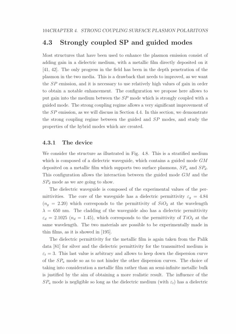
104CHAPTER 4. STRONG COUPLING SURFACE PLASMON POLARITONS
4.3 Strongly coupled SP and guided modes
Most structures that have been used to enhance the plasmon emission consist of
adding gain in a dielectric medium, with a metallic film directly deposited on it
[41, 42]. The only progress in the field has been in the depth penetration of the
plasmon in the two media. This is a drawback that needs to improved, as we want
the SP emission, and it is necessary to use relatively high values of gain in order
to obtain a notable enhancement. The configuration we propose here allows to
put gain into the medium between the SP mode which is strongly coupled with a
guided mode. The strong coupling regime allows a very significant improvement of
the SP emission, as we will discuss in Section 4.4. In this section, we demonstrate
the strong coupling regime between the guided and SP modes, and study the
properties of the hybrid modes which are created.
4.3.1 The device
We consider the structure as illustrated in Fig. 4.8. This is a stratified medium
which is composed of a dielectric waveguide, which contains a guided mode GM
deposited on a metallic film which supports two surface plasmons, SPu and SPd.
This configuration allows the interaction between the guided mode GM and the
SPd mode as we are going to show.
The dielectric waveguide is composed of the experimental values of the per-
mittivities. The core of the waveguide has a dielectric permittivity εg = 4.84
(ng = 2.20) which corresponds to the permittivity of SiO2 at the wavelength
λ = 650 nm. The cladding of the waveguide also has a dielectric permittivity
εd = 2.1025 (nd = 1.45), which corresponds to the permittivity of T iO2 at the
same wavelength. The two materials are possible to be experimentally made in
thin films, as it is showed in [195].
The dielectric permittivity for the metallic film is again taken from the Palik
data [81] for silver and the dielectric permittivity for the transmitted medium is
εt = 3. This last value is arbitrary and allows to keep down the dispersion curve
of the SPu mode so as to not hinder the other dispersion curves. The choice of
taking into consideration a metallic film rather than an semi-infinite metallic bulk
is justified by the aim of obtaining a more realistic result. The influence of the
SPu mode is negligible so long as the dielectric medium (with εt) has a dielectric

4.3. STRONGLY COUPLED SP AND GUIDED MODES 105
GM
SPd
SPuεt
eg
εm
εd
εg
ed
εd x0
em
y
Figure 4.8: Planar guided structure which allows a strong coupling regime between the surfaceplasmon SPd and the guided mode GM . The permittivities of each of the layers are εd = 2.1025,εg = 4.84, εt = 3, and εm is taken from the Palik data [81] for silver. The thickness of the coreof the waveguide eg and the metallic thickness em are fixed. Only the thickness ed, the distancebetween the two coupled modes, has to change in order to determine the best configuration forthe strong coupling regime.
permittivity higher than the cladding of the waveguide (with εd).
The coupled plasmons/guided mode dispersions can be represented with a cou-
pled oscillator model [196]. The dispersion relations are obtained by diagonalizing
the plasmons-guided mode Hamiltonians:
H =
EGM − iγGM VSPd/2 0
VSPdESPd
− iγSPd0
0 0 ESPu− iγSPu
, (4.42)
where EGM is the guided mode energy, γGM is the guided mode linewidth, ESPd
and ESPuare the SP modes energies, γSPd
and γSPuare the plasmon linewidth and
VSPdis the interaction energy between the SPd mode and the guided mode GM .
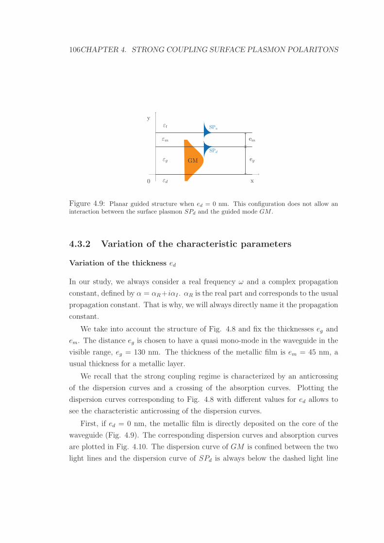
106CHAPTER 4. STRONG COUPLING SURFACE PLASMON POLARITONS
GM
SPd
SPuεt
eg
εm
εg
em
εd x0
y
Figure 4.9: Planar guided structure when ed = 0 nm. This configuration does not allow aninteraction between the surface plasmon SPd and the guided mode GM .
4.3.2 Variation of the characteristic parameters
Variation of the thickness ed
In our study, we always consider a real frequency ω and a complex propagation
constant, defined by α = αR+iαI . αR is the real part and corresponds to the usual
propagation constant. That is why, we will always directly name it the propagation
constant.
We take into account the structure of Fig. 4.8 and fix the thicknesses eg and
em. The distance eg is chosen to have a quasi mono-mode in the waveguide in the
visible range, eg = 130 nm. The thickness of the metallic film is em = 45 nm, a
usual thickness for a metallic layer.
We recall that the strong coupling regime is characterized by an anticrossing
of the dispersion curves and a crossing of the absorption curves. Plotting the
dispersion curves corresponding to Fig. 4.8 with different values for ed allows to
see the characteristic anticrossing of the dispersion curves.
First, if ed = 0 nm, the metallic film is directly deposited on the core of the
waveguide (Fig. 4.9). The corresponding dispersion curves and absorption curves
are plotted in Fig. 4.10. The dispersion curve of GM is confined between the two
light lines and the dispersion curve of SPd is always below the dashed light line
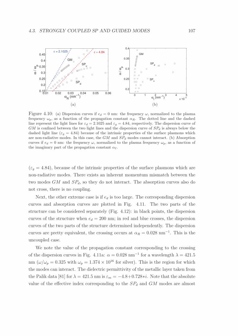
4.3. STRONGLY COUPLED SP AND GUIDED MODES 107
0.01 0.02 0.03 0.04 0.05 0.060.15
0.2
0.25
0.3
0.35
0.4
0.45
ω /
ωp
αR
(nm−1
)
ε = 4.84ε = 2.1025
SPu
GM
SPd
(a)
0 1 2 3 4 5
x 10−3
0.2
0.25
0.3
0.35
0.4
αI (nm
−1)
ω /
ωp
GM
SPu
SPd
(b)
Figure 4.10: (a) Dispersion curves if ed = 0 nm: the frequency ω, normalized to the plasmafrequency ωp, as a function of the propagation constant αR. The dotted line and the dashedline represent the light lines for εd = 2.1025 and εg = 4.84, respectively. The dispersion curve ofGM is confined between the two light lines and the dispersion curve of SPd is always below thedashed light line (εg = 4.84) because of the intrinsic properties of the surface plasmons whichare non-radiative modes. In this case, the GM and SPd modes cannot interact. (b) Absorptioncurves if ed = 0 nm: the frequency ω, normalized to the plasma frequency ωp, as a function ofthe imaginary part of the propagation constant αI .
(εg = 4.84), because of the intrinsic properties of the surface plasmons which are
non-radiative modes. There exists an inherent momentum mismatch between the
two modes GM and SPd, so they do not interact. The absorption curves also do
not cross, there is no coupling.
Next, the other extreme case is if ed is too large. The corresponding dispersion
curves and absorption curves are plotted in Fig. 4.11. The two parts of the
structure can be considered separately (Fig. 4.12): in black points, the dispersion
curves of the structure when ed = 200 nm; in red and blue crosses, the dispersion
curves of the two parts of the structure determined independently. The dispersion
curves are pretty equivalent, the crossing occurs at αR = 0.028 nm−1. This is the
uncoupled case.
We note the value of the propagation constant corresponding to the crossing
of the dispersion curves in Fig. 4.11a: α = 0.028 nm−1 for a wavelength λ = 421.5
nm (ω/ωp = 0.325 with ωp = 1.374× 10¹⁶ for silver). This is the region for which
the modes can interact. The dielectric permittivity of the metallic layer taken from
the Palik data [81] for λ = 421.5 nm is εm = −4.8+0.728∗i. Note that the absolutevalue of the effective index corresponding to the SPd and GM modes are almost
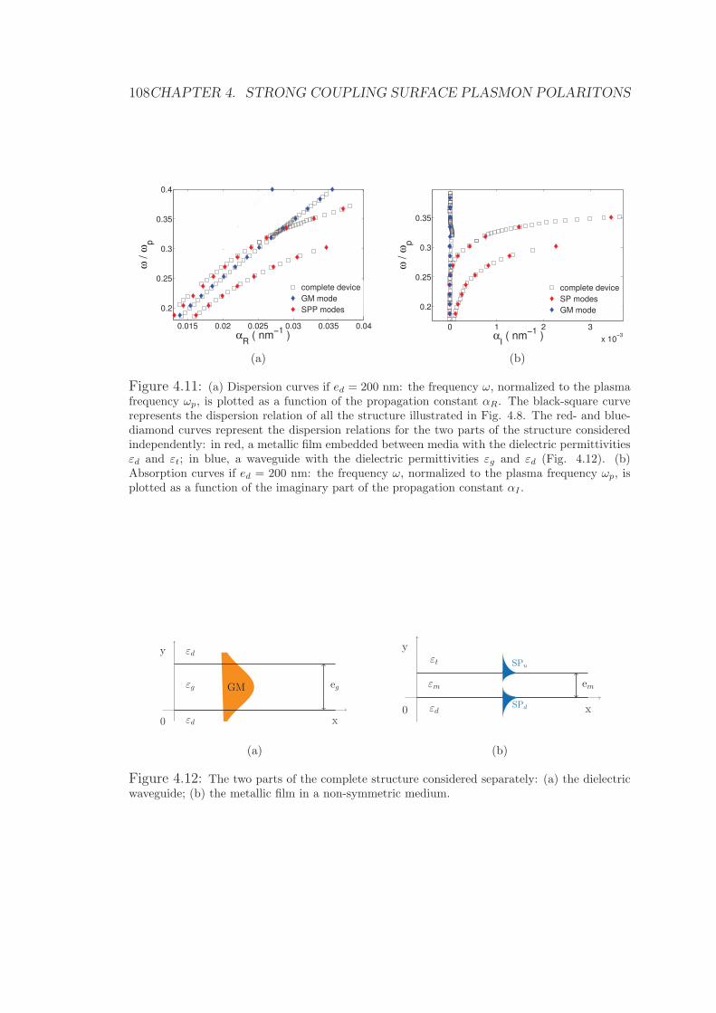
108CHAPTER 4. STRONG COUPLING SURFACE PLASMON POLARITONS
0.015 0.02 0.025 0.03 0.035 0.04
0.2
0.25
0.3
0.35
0.4
αR
( nm−1
)
ω /
ωp
complete device
GM mode
SPP modes
(a)
0 1 2 3
x 10−3
0.2
0.25
0.3
0.35
αI ( nm
−1 )
ω /
ωp
complete device
SP modes
GM mode
(b)
Figure 4.11: (a) Dispersion curves if ed = 200 nm: the frequency ω, normalized to the plasmafrequency ωp, is plotted as a function of the propagation constant αR. The black-square curverepresents the dispersion relation of all the structure illustrated in Fig. 4.8. The red- and blue-diamond curves represent the dispersion relations for the two parts of the structure consideredindependently: in red, a metallic film embedded between media with the dielectric permittivitiesεd and εt; in blue, a waveguide with the dielectric permittivities εg and εd (Fig. 4.12). (b)Absorption curves if ed = 200 nm: the frequency ω, normalized to the plasma frequency ωp, isplotted as a function of the imaginary part of the propagation constant αI .
GM eg
εd
εg
εd x0
y
(a)
SPd
SPuεt
εm
εd
em
x0
y
(b)
Figure 4.12: The two parts of the complete structure considered separately: (a) the dielectricwaveguide; (b) the metallic film in a non-symmetric medium.

4.3. STRONGLY COUPLED SP AND GUIDED MODES 109
50 100 150 200
0.026
0.027
0.028
0.029
0.03
ed ( nm )
αR
( n
m−
1 )
(a)
50 100 150 200
0
2
4
6
8
10
x 10−4
ed ( nm )
αI (
nm
−1 )
(b)
Figure 4.13: (a) The propagation constant αR as a function of the distance ed. The splittingbetween the curves for the GM and SPd modes decreases with the increase of ed. (b) Theimaginary part of the propagation constant αI as a function of the distance ed. The crossing ofthe absorption curves for the GM and the SPd modes occurs at ed = 100 nm, the optimal valueto obtain a strong coupling regime between the GM and SPd modes.
equal at this wavelength. This is an important condition in order to obtain the
coupling. We plot the propagation constants of the three modes as a function of
the thickness ed at the wavelength λ = 421.5 nm in Fig. 4.13a. Without surprise,
the splitting between the GM and SPd modes decreases with the increase of the
distance ed.
To find the corresponding value of the strong coupling regime, we have to
consider the absorption curves which are deduced from the imaginary parts αI
of the propagation constant. This is the reason why the tetrachotomy method is
useful, since it allows to find the poles of the S-matrix with simultaneously the real
and imaginary parts. Fig. 4.13b shows the imaginary parts αI corresponding to
the propagation constants as a function of the distance ed. The crossing of the two
absorption curves for GM and SPd corresponds to the strong coupling between
the two modes. The GM mode sees its absorption increases, when the absorption
for the SPd mode decreases, until the intersection for ed = 100 nm.
The structure evolves from the case in which the SPd mode cannot be directly
excited by the GM when ed = 0 nm, to the uncoupled case where the two modes
are too far from each other to interact. Between these two extreme cases, there is a
range for the distance ed where the SPd mode can exist in the medium characterized
by εd, because ed becomes higher than its penetration length. In this range, the

110CHAPTER 4. STRONG COUPLING SURFACE PLASMON POLARITONS
0.02 0.03 0.04 0.05
0.2
0.25
0.3
0.35
0.4
αR
( nm−1
)
ω /
ωp
complete device
GM mode
SPP modes
Figure 4.14: Dispersion curves if ed = 100 nm, the optimal thickness for obtaining the strongcoupling regime: the frequency ω, normalized to the plasma frequency ωp, is plotted as a functionof the propagation constant αR. In blue and red, the dispersion curves of the modes before thecoupling with a crossing between them. The anticrossing of the dispersion curves (black squares)is a feature of the strong coupling between the GM and SPd modes. The new modes also createdare hybrid modes between the initial ones. The Rabi splitting is ER = 134 meV.
0 5 10 15 20
x 10−4
0.25
0.3
0.35
0.4
αI ( nm
−1 )
ω /
ωp
complete device
GM mode
SPP modes
Figure 4.15: Absorption curves if ed = 100 nm, the optimal thickness for obtaining the strongcoupling regime: the frequency ω, normalized to the plasma frequency ωp, is plotted as a functionof the imaginary part of propagation constant αI . The crossing of the absorption curves is anotherfeature of the strong coupling between the GM and SPd modes. GM exchanges energy withSPd and its losses increase when the losses for the surface plasmon decrease if we compare withthe blue and red curves corresponding of the modes before the coupling.

4.3. STRONGLY COUPLED SP AND GUIDED MODES 111
SPd mode can interact with the GM mode. Its dispersion curve can cross the one
of the guided mode. We note that the behavior of the SPu mode is independent
from the parameter ed.
We plot the dispersion curves and the absorption curves for ed = 100 nm in
Figs. 4.14 and 4.15, respectively. We also see the characteristic anticrossing of the
dispersion curves of GM and SPd, with a deformation of the curves as compared
to the uncoupled ones. The two modes corresponding to the propagation constant
αR = 0.028 nm−1 are new modes of the structure, hybrid modes between the initial
modes. We denote them SPd,c and GMc the lower and the higher modes at the
wavelength λl = 421.5 nm and λh = 405 nm, respectively. The Rabi splitting is
ER = 134 meV.
This anticrossing is associated to the crossing of the absorption curves at the
same value of the propagation constant αR = 0.028 nm−1. The frequency is plotted
as a function of the imaginary part of the propagation constant, so as to better
see the movement of the absorption curves between the uncoupling case and the
strong coupling case with the crossing. This crossing is another feature of the
strong coupling regime. However, the coupling implies a guided mode which does
not have losses and a surface plasmon which has intrinsic losses. We also see that
the exchange of energy between these modes involves an increase of the losses for
GM and, at the same time, the decrease of the losses for SPd. GM gives energy
to SPu. The propagation length has to be enhanced in this configuration, as we
will see.
The possibility of obtaining a strong coupling regime between SPd and GM
modes has been demonstrated. We will study the properties of the hybrid modes
SPd,c and GMc in Part 4.3.3. In particular, we need to verify whether or not the
SPd,c mode is still a surface mode, and to quantify its confinement.
Variation of the range of frequency
The result obtained previously can be transposed to other ranges of frequency
without losing in generalities. The strong coupling regime can be obtained with
an appropriate modulation of the distance between the core of the waveguide and
the metallic film.

112CHAPTER 4. STRONG COUPLING SURFACE PLASMON POLARITONS
0.02 0.04
0.2
0.4
αR
( nm−1
)
ω / ω
p
GMc
SPd,c
Figure 4.16: Range of the frequencies enabling to observe temporal oscillations in the strongcoupling regime at the propagation constant αR = 0.028 nm−1.
4.3.3 Numerical results for the optimal coupling
Temporal oscillations of the modes
The direct consequence of the strong coupling regime is temporal oscillations. The-
ses oscillations correspond to the case in which we consider a constant value of the
propagation constant and observe the variations of the corresponding frequencies
as illustrated in Fig 4.16. These can be observed with the Finite Difference Time
Domain (FDTD) method. We adapt it to the case of dispersive media to take the
metallic film into account. Details about the implementation of the FDTD method
are given in appendix A.
We consider the complete device (Fig. 4.8) in the case of the strong coupling
regime between the SPd and the GM modes when the distance ed = 100 nm. The
temporal oscillations between the hybrid modes SPd,c and GMc are represented in
Fig. 4.17. The size of the cell is ∆l = 5 nm and the corresponding time step is
∆t = ∆l/(2c), with c the speed of light in vacuum. The permittivity of the metallic
layer is taken from the Drude model. The magnitude of the field corresponding to
the plasmon mode is lower than the magnitude of the field in the waveguide. The
period of the oscillations is Tt = 30.7 fs1.
Fig. 4.18 illustrates snapshots of the structure when the elapsed time is t1 =
62.5 fs and t2 = 83 fs. In Fig. 4.18a, the SPd,c mode is excited for the first time
when in Fig. 4.18b, the surface plasmon mode is excited again after one period Tt.
1If we consider the energy as E = ~ω = ~2 ∗ pi/Tt, we find ER = 134.7 meV.

4.3. STRONGLY COUPLED SP AND GUIDED MODES 113
0 100 200 300 400 500 600 700 800
−0.05
0
0.05
0.1
t ( fs )
Fie
ld’s
am
plit
ud
e
center of the waveguide
surface of the metallic layer
Figure 4.17: Temporal oscillations between the hybrid modes deduced from the FDTD calcu-lations. The period of the oscillations is Tt = 30.7 fs.
Spatial oscillations of the modes
In the case of the strong coupling between plasmons and excitons recalled in the
previous section, the initial excitons do not have dispersion so their dispersion rela-
tion is constant depending on the propagation constant. The temporal oscillations
between the modes can be easily observed or determined with the coupled-mode
theory. In the case of our complete device (Fig. 4.8), which allows the strong
coupling between plasmons and guided modes, the inclination of the dispersion
relations in comparison with the non-dispersive plane implies the possibility of
observing spatial oscillations, as we will present in this part.
The aim is to excite only the modes in a precise range of the propagation
constant, including the two hybrid modes (Fig. 4.19). The range of the gaussian
beam is reduced and we name it an evanescent gaussian beam.
We consider the complete device (Fig. 4.8) in the case of the strong coupling
regime between the SPd and the GM modes when the distance ed = 100 nm.
The spatial oscillations between the hybrid modes SPd,c and GMc are represented
in Fig. 4.20, with a dielectric permittivity of the metallic film taken from the
Drude model. We see oscillations between the two modes and can already observe
a good confinement for the hybrid SPd,c mode, the energy of the guided mode
being transferred to the hybrid plasmon SPd,c which spends twice less time on the
metallic surface. Its intrinsic decay has to be reduced.
This result is calculated from the Drude model and is idealized. If we consider

114CHAPTER 4. STRONG COUPLING SURFACE PLASMON POLARITONS
(a)
(b)
Figure 4.18: Snapshots of the structure after two elapsed times: (a) t1 = 62.5 fs, the SPd modeis excited for the first time. (b) t2 = 83 fs, the SPd mode is excited again after one period Tt.The structure is mapped in two parts because of the relative weakness of the field’s amplitudefor the surface mode, as compared to the guided mode.
the Palik data [81] for calculating the permittivity of the metallic layer, the result
is shown in Fig. 4.21. The spatial oscillations between the modes are no longer as
marked and a steady state of the system is difficult to see. This result shows that
the spatial oscillations are present, but the losses of the metal rapidly attenuate
the field. Fig. 4.22 illustrates in one dimension the spatial oscillations between
the two modes, with the Drude model and the Palik data. The period of the
oscillations is Ts = 1.7µm.
With an evanescent gaussian beam, we can also observe the modes far away
from the region of the strong coupling regime. Fig. 4.23a shows the region of the
dispersion relation we want to observe. We are looking to excite the fundamental

4.3. STRONGLY COUPLED SP AND GUIDED MODES 115
0.02 0.04
0.2
0.4
αR
( nm−1
)
ω / ω
p
Figure 4.19: Range of the propagation constant, including the two hybrid modes in order toobserve spatial oscillations between them, at the wavelength λl = 421.5 nm.
Figure 4.20: Map of the field with an incident evanescent gaussian beam used to observe thespatial oscillations in the complete structure when ed = 100 nm. The metallic permittivity εm istaken from the Drude model. The energy of the hybrid guided mode is transferred to the hybridplasmon which passes approximatively twice less time on the metallic surface. Its intrinsic decayhas to be reduced.

116CHAPTER 4. STRONG COUPLING SURFACE PLASMON POLARITONS
Figure 4.21: Spatial oscillations between the two hybrid modes when the strong couplingregime occurs, using the Palik data for the metallic permittivity [81]. The propagation length ofthe hybrid SPd,c mode is approximatively 1µm, against only 400 nm in the uncoupled case.
0 0.5 1 1.5 2 2.5
x 104
0
0.2
0.4
0.6
0.8
1x 10
−3
x ( nm )
H
2
center of the waveguide
surface of the metallic layer
(a)
0 2000 4000 6000 8000
0
2
4
6
8
10
12
x 10−4
x ( nm )
H
2
center of the waveguide
surface of the metallic layer
(b)
Figure 4.22: Spatial oscillations between the two hybrid modes when the strong couplingregime occurs (a) with the Drude model and (b) the Palik data for silver permittivity [81]. GMc
exchanges energy with SPd,c, with a period Ts = 1.7µm.

4.3. STRONGLY COUPLED SP AND GUIDED MODES 117
0.02 0.04
0.2
0.4
αR
( nm−1
)
ω / ω
p
Excitation of the fundamentel guided mode
(a)
0 0.5 1 1.5 2 2.5
x 104
1.5
2
2.5
3
3.5
4
4.5x 10
−3
x ( nm )
H
2
(b)
(c)
Figure 4.23: The fundamental guided mode far away from the anticrossing, excited by anevanescent gaussian beam with the Palik data [81]. (a) In the dispersion curves, we consider thepoint noted by a red dot characterized by αR = 0.0346 nm−1, at a wavelength λ = 349.5 nm. (b)In one dimension, the intensity of the field in the center of the waveguide. (c) The correspondingmap of the field in the plane (x, y).
guided mode. Once again, we use the Palik data for the metallic permittivity [81].
In Fig. 4.23b, the intensity of the field in the center of the dielectric waveguide
is plotted as a function of the distance x. The corresponding map of the field is
in Fig. 4.23c. Having no losses, the guided mode has a propagation length and a
shape strongly related to what was expected.
Confinement of the SPd,c mode
The confinement of the SPd,c mode relates to the depth penetration of the surface
plasmon in the dielectric, with εd (εd = 2.1025). Theoretically, the depth pene-

118CHAPTER 4. STRONG COUPLING SURFACE PLASMON POLARITONS
60 80 100 120 140 1600
500
1000
1500
2000
ed ( nm )
δ (
nm
)
GM GM
SPd
SPu
SPd
Figure 4.24: Propagation length δ as a function of the distance ed for the modes in the completestructure (Fig. 4.8) for λl = 421.5 nm. The crossing of the curves corresponds to the maximumof the propagation length for the SPd,c mode, what occurs for ed = 100 nm, δSP = 1036 nm.
tration of an uncoupled SP in this configuration is δd,uncoupled = 80 nm. With the
maps of the field (Figs. 4.20 and 4.21), we deduced that the field of SPd,c mode
decays of 1/e along the y-direction after a distance δd ∼ 50 nm. The confinement
of the plasmon is fairly good, better than the one in an uncoupled structure. The
hybrid mode also created is still a surface mode and keeps the main property of
the classical SPs.
Enhancement of the propagation length
In Fig. 4.21, the hybrid SPd,c mode has a propagation length equalling approxima-
tively to 1µm, when in the uncoupled case2, its propagation length is only 400 nm.
To confirm this result, we use the tetrachotomy method to determine the propa-
gation constant as a function of the thickness ed at the wavelength λl = 421.5 nm.
The result is plotted in Fig. 4.24.
For a SP mode at the interface between a metallic medium with εm (εm is
taken from the Palik data) and a dielectric medium with εd (εd = 2.1025), the
theoretical propagation length (Eq. 2.13) is 300 nm. The crossing of the curves
corresponds to the maximum of the propagation length for the SPd,c mode that
occurs for ed = 100 nm, δSPd,c= 1036 nm. The table 4.1 includes the propagation
2The uncoupled structure is a metallic layer embedded between a two dielectric media withthe permittivities εd and εa (see Fig. 4.12b)
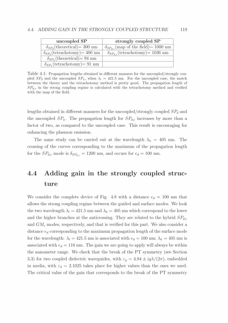
4.4. ADDING GAIN IN THE STRONGLY COUPLED STRUCTURE 119
uncoupled SP strongly coupled SPδSPd
(theoretical)= 300 nm δSPd,c(map of the field)∼ 1000 nm
δSPd(tetrachotomy)= 400 nm δSPd,c
(tetrachotomy)= 1036 nmδSPu
(theoretical)= 94 nmδSPu
(tetrachotomy)= 91 nm
Table 4.1: Propagation lengths obtained in different manners for the uncoupled/strongly cou-pled SPd and the uncoupled SPu, when λl = 421.5 nm. For the uncoupled case, the matchbetween the theory and the tetrachotomy method is pretty good. The propagation length ofSPd,c in the strong coupling regime is calculated with the tetrachotomy method and verifiedwith the map of the field.
lengths obtained in different manners for the uncoupled/strongly coupled SPd and
the uncoupled SPu. The propagation length for SPd,c increases by more than a
factor of two, as compared to the uncoupled case. This result is encouraging for
enhancing the plasmon emission.
The same study can be carried out at the wavelength λh = 405 nm. The
crossing of the curves corresponding to the maximum of the propagation length
for the SPd,c mode is δSPd,c= 1200 nm, and occurs for ed = 100 nm.
4.4 Adding gain in the strongly coupled struc-
ture
We consider the complete device of Fig. 4.8 with a distance ed = 100 nm that
allows the strong coupling regime between the guided and surface modes. We look
the two wavelength λl = 421.5 nm and λh = 405 nm which correspond to the lower
and the higher branches at the anticrossing. They are related to the hybrid SPd,c
and GMc modes, respectively, and that is verified for this part. We also consider a
distance ed corresponding to the maximum propagation length of the surface mode
for the wavelength: λl = 421.5 nm is associated with ed = 100 nm; λh = 405 nm is
associated with ed = 110 nm. The gain we are going to apply will always be within
the nanometer range. We check that the break of the PT symmetry (see Section
3.3) for two coupled dielectric waveguides, with εg = 4.84 ± igλ/(2π), embedded
in media, with εd = 2.1025 takes place for higher values than the ones we used.
The critical value of the gain that corresponds to the break of the PT symmetry
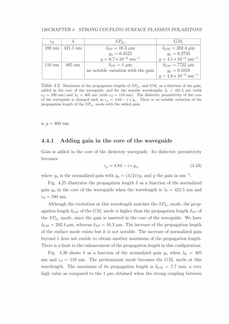
120CHAPTER 4. STRONG COUPLING SURFACE PLASMON POLARITONS
ed λ SPd,c GMc
100 nm 421.5 nm δSP = 16.3 µm δGM = 202.4 µmgn = 0.4522 gn = 0.2733
g = 6.7 ∗ 10−3 nm−1 g = 4.1 ∗ 10−3 nm−1
110 nm 405 nm δSP = 1 µm δGM = 7722 µmno notable variation with the gain gn = 0.1018
g = 1.6 ∗ 10−3 nm−1
Table 4.2: Maximum of the propagation lengths of SPd,c and GMc as a function of the gain,added in the core of the waveguide, and for the notable wavelengths λl = 421.5 nm (withed = 100 nm) and λh = 405 nm (with ed = 110 nm). The dielectric permittivity of the coreof the waveguide is changed such as εg = 4.84 − i ∗ gn. There is no notable variation of thepropagation length of the SPd,c mode with the added gain.
is g ∼ 400 nm.
4.4.1 Adding gain in the core of the waveguide
Gain is added in the core of the dielectric waveguide. Its dielectric permittivity
becomes:
εg = 4.84− i ∗ gn, (4.43)
where gn is the normalized gain with gn = (λ/2π)g, and g the gain in nm−1.
Fig. 4.25 illustrates the propagation length δ as a function of the normalized
gain gn in the core of the waveguide when the wavelength is λl = 421.5 nm and
ed = 100 nm.
Although the excitation at this wavelength matches the SPd,c mode, the prop-
agation length δGM of the GMc mode is higher than the propagation length δSP of
the SPd,c mode, since the gain is inserted in the core of the waveguide. We have
δGM = 202.4 µm, whereas δSP = 16.3 µm. The increase of the propagation length
of the surface mode exists but it is not notable. The increase of normalized gain
beyond 1 does not enable to obtain another maximum of the propagation length.
There is a limit to the enhancement of the propagation length in this configuration.
Fig. 4.26 shows δ as a function of the normalized gain gn when λh = 405
nm and ed = 110 nm. The predominant mode becomes the GMc mode at this
wavelength. The maximum of its propagation length is δGM = 7.7 mm, a very
high value as compared to the 1 µm obtained when the strong coupling between

4.4. ADDING GAIN IN THE STRONGLY COUPLED STRUCTURE 121
0 0.2 0.4 0.6 0.8 10
50
100
150
200
gn
δ (
µm
)GM
c
SPd,c
Figure 4.25: The propagation length δ of the modes as a function of the gain in the core ofthe waveguide when λl = 421.5 nm and ed = 100 nm. The maximum of the propagation lengthsare δGM = 202.4 µm for gn = 0.2733 and δSP = 16.3 µm for gn = 0.4522.
0 0.2 0.4 0.6 0.8 10
2000
4000
6000
8000
gn
δ (
µm
)
GMc
Figure 4.26: The propagation length δ of the modes as a function of the gain in the core ofthe waveguide when λh = 405 nm and ed = 110 nm. The maximum of the propagation lengthfor the GMc mode is δGM = 7722 µm for gn = 0.1018.

122CHAPTER 4. STRONG COUPLING SURFACE PLASMON POLARITONS
ed λ SPd,c GMc
100 nm 421.5 nm δSP = 6461 µm δGM = 4149 µmgn = 0.1031 gn = 0.118
g = 1.5 ∗ 10−3 nm−1 g = 1.8 ∗ 10−3 nm−1
110 nm 405 nm δSP = 1435 µm δGM = 4400 µmgn = 0.1578 gn = 0.1386
g = 2.4 ∗ 10−3 nm−1 g = 2.2 ∗ 10−3 nm−1
Table 4.3: Maximum of the propagation lengths of SPd,c and GMc as a function of the gainadded into the dielectric layer between the two strongly coupled modes, and for the notablewavelengths λl = 421.5 nm (with ed = 100 nm) and λh = 405 nm (with ed = 110 nm). Thedielectric permittivity of the dielectric layer is changed such as εd = 2.1025− i ∗ gn.
this mode and the surface plasmon occurs. The propagation length of the surface
mode is not amplified at all, δSP = 1 µm. The results are summarized in table 4.2.
This configuration cancels the losses for the guided mode due to the strong
coupling with the SPd mode. The propagation length δSP of the SPd,c can be
enhanced sixteen times as compared to the strong coupling case without gain, but
the introduction of gain in the medium between the two strongly coupled modes
has to improve the SP mode.
4.4.2 Adding gain in the medium between the two strongly
coupled modes
We add gain in the medium of permittivity εd, with the thickness ed, between
the two strongly coupled modes. Fig. 4.27 shows the propagation length δ of the
modes as a function of the normalized gain gn in the layer, when λl = 421.5 nm
and ed = 100 nm. At this wavelength, the SPd,c mode is predominant and its
propagation length is δSP = 6461 µm for gn = 0.1031.
The propagation length δ of the modes when λh = 405 nm and ed = 110 nm
is plotted in Fig. 4.28. The propagation length corresponding to the guided mode
δGM stays almost constant at the two wavelengths when δSP goes down 1435 µm
when λh = 405 nm. The results are summarized in table 4.3.
The understanding of the improvement of propagation lengths passes by the
study of the evolution of the dispersion and absorption curves (Figs. 4.29 and
4.30), as well as the evolution of the poles in the complex plane (αR, αI), plotted

4.4. ADDING GAIN IN THE STRONGLY COUPLED STRUCTURE 123
0.05 0.1 0.15 0.20
1000
2000
3000
4000
5000
6000
gn
δ (
µm
)SP
d,c
GMc
Figure 4.27: The propagation length δ of the modes as a function of the gain in the layerbetween the two strongly coupled modes when λl = 421.5 nm and ed = 100 nm. The maximum ofthe propagation lengths are δGM = 4149 µm for gn = 0.118 and δSP = 6461 µm for gn = 0.1031.
0.1 0.12 0.14 0.16 0.18 0.20
1000
2000
3000
4000
gn
δ (
µm
)
GMc
SPd,c
Figure 4.28: The propagation length δ of the modes as a function of the gain in the layerbetween the two strongly coupled modes when λl = 405 nm and ed = 110 nm. The maximum ofthe propagation lengths are δGM = 4400 µm for gn = 0.1386, and δSP = 1435 µm for gn = 0.1578.

124CHAPTER 4. STRONG COUPLING SURFACE PLASMON POLARITONS
0.015 0.02 0.025 0.03 0.035 0.04 0.045
0.25
0.3
0.35
αR
( nm−1
)
ω /
ωp
gn=0
gn=0.1
gn=5
Figure 4.29: Dispersion curves of the complete device as a function of the gain in the dielectriclayer between the two strongly coupled modes. First, the anticrossing increases up to a normalizedgain gn = 0.14. Then, the dispersion curve of the SPu mode moves towards lower values of thepropagation constant.
in Fig. 4.31.
The anticrossing of the dispersion curves (Fig. 4.29) increases with the gain to
attain a Rabi splitting ER,a = 145 meV, when gn = 0.14, when the losses for the
surface mode are the most compensated. The crossing of the absorption curves
(Fig. 4.30) moves to lower losses with the increase of the gain, and reaches almost
zero when gn = 0.14. The conservation of the crossing up to this value of the gain
is a proof of the strong coupling regime between these modes despite the added
gain.
The poles of the S-matrix plotted in the complex plane (αR, αI) move as a
function of the gain. First, the poles corresponding to the hybrid coupled modes
move down until reaching the real axis, when gn = 0.14. Then, these poles do not
evolve anymore, whereas the poles for the SPu mode move towards a minimum
of absorption, before a new increase of the losses with a decreasing propagation
constant (as is confirmed with the dispersion curve).
Fig. 4.32 represents the map of the field obtained with an incident evanescent
beam for observing the spatial oscillations, for a gain gn = 0.1031 at the wavelength
λl = 421.5 nm. The metallic permittivity εm is taken from the Palik data [81].
The energy of the hybrid guided mode is transferred with an amplified dielectric
separating medium to the hybrid plasmon. The period of the oscillations increases

4.4. ADDING GAIN IN THE STRONGLY COUPLED STRUCTURE 125
0 1 2 3
x 10−3
0.2
0.25
0.3
0.35
0.4
ω /
ωp
αI ( nm
−1 )
gn=0
gn=0.1
gn=5
Figure 4.30: Absorption curves of the complete device as a function of the gain in the dielectriclayer between the two strongly coupled modes. First, the crossing moves towards lower values ofthe absorption up to a normalized gain gn = 0.14. Then, the absorption curve of the SPu modealso moves towards lower values of the absorption.
0.025 0.03 0.035 0.04 0.045−1
0
1
2
3
4
5
6x 10
−3
αR
( nm−1
)
αI (
nm
−1 )
gn ∈ [1.5,20]
gn ∈ [0.2,1]
gn ∈ [0,0.15]
1 2
3
Figure 4.31: Poles of the S-matrix of the complete device in the strong coupling, as a functionof the gain in the dielectric layer between the two strongly coupled modes. The hybrid guidedmode GMc and the hybrid surface mode SPd,c are noted 1 and 2 without gain, respectively.The upper surface mode SPu is noted 3. First, the poles corresponding to the hybrid coupledmodes move down until attaining the real axis when gn = 0.14. Then, these poles do not moveanymore, whereas the poles for the SPu mode move towards a minimum of absorption, before anew increase of the losses, with a decreasing propagation constant.

126CHAPTER 4. STRONG COUPLING SURFACE PLASMON POLARITONS
Figure 4.32: Map of the field obtained with an incident evanescent beam to observe the spatialoscillations for a gain gn = 0.1031 at the wavelength λl = 421.5 nm. The metallic permittivityεm is taken from the Palik data [81]. The energy of the hybrid guided mode is transferred withan amplified dielectric separating medium to the hybrid plasmon. The period of the oscillationsis Ts,a = 2.6 µm.
to Ts,a = 2.6 µm, whereas the spatial oscillations with the Palik data for the metal
rapidly vanish without gain (Fig. 4.21). The amplitude of the field corresponding
to the hybrid plasmon becomes greater than the amplitude of the hybrid guided
mode, which is coherent with a greater propagation length in this configuration.
The results obtained in Figs. 4.26, 4.25, 4.28 and 4.27 are with a constant value
of the wavelength (421.5 or 405 nm). If we consider Fig. 4.30, we see that at a
given value of frequency, we do not follow the crossing of the absorption curves.
The two successive peaks in the plot of the propagation length as a function of
the added gain also correspond to both quasi-coupled modes which have different
values of propagation constant.
Fig. 4.33 shows the propagation length δ of the hybrid modes as a function of
the gain in the layer between both strongly coupled modes when the wavelength
changes with the crossing of the absorption curves as a function of the added
gain. We find that the propagation length increases until the value we consider
as the limit in the plot of the poles in the complex plane (Fig. 4.31), gn = 0.14.
The propagation length for the hybrid plasmon is δSPd,c= 1237 µm. Fig. 4.34
represents the map of the field obtained with an incident evanescent beam for
observing the spatial oscillations, for a gain gn = 0.14 at the wavelength λl = 409
nm, the corresponding value of the wavelength to the crossing of the absorption

4.4. ADDING GAIN IN THE STRONGLY COUPLED STRUCTURE 127
0.08 0.1 0.12 0.14 0.16 0.180
200
400
600
800
1000
1200
1400
gn
δ (
µm
)
Figure 4.33: The propagation length δ of the hybrid modes as a function of the gain in thelayer between both strongly coupled modes when the wavelength corresponds to the crossing ofthe absorption curves as a function of the added gain. The maximum of the propagation lengthsare at the same value of the propagation constant, δSPd,c
= 1237 µm.
curves. After this critical value, the gain starts to enhance the emission of the SPu
mode (Fig. 4.30).
4.4.3 Adding gain without a strong coupling device
The necessity of a device, which allows a strong coupling regime, is demonstrated
with the plot of the propagation length as a function of the gain in two cases:
firstly, an incident medium with a permittivity εd and a layer of thickness ed with
a permittivity ε = εd− i∗gn deposited directly against the metallic layer; secondly,
an incident medium directly with the gain, ε = εd − i ∗ gn against the metallic
layer. The results are summarized in Table 4.4. In both cases, the increase of
the propagation length for the SPd mode is not comparable to the result obtained
with the complete waveguide in strong coupling regime.
In conclusion, we demonstrate the possibility to enhance the SP emission in
the strong coupling regime with added gain. Next, the necessity of the strong
coupling configuration for obtaining this improvement has also been demonstrated.
It is important to note that the surface plasmon SPd is not the most efficient
type of plasmon we can obtain in the visible range3, because it is taken too high
on the dispersion curve. However, it is easy to observe with these characteristic
3as compared to the SP in the air for a wavelength λ = 633 nm)

128CHAPTER 4. STRONG COUPLING SURFACE PLASMON POLARITONS
Figure 4.34: Map of the field obtained with an incident evanescent beam to observe the spatialoscillations for a gain gn = 0.14 at the wavelength λl = 409 nm, the corresponding value of thewavelength to the crossing of the absorption curves.
ed λ δSPugn
100 nm 421.5 nm 3.38 µm gn = 0.15110 nm 405 nm 36.1 µm gn = 0.12
no ed 421.5 nm 3.9 µm gn = 0.15no ed 405 nm 12.9 µm gn = 0.11
Table 4.4: Maximum of the propagation lengths of SPd,c as a function of the gain without thedielectric waveguide (no layer with εg = 4.84) and for the notable wavelengths λl = 421.5 nm(with ed = 100 nm) and λh = 405 nm (with ed = 110 nm). The dielectric permittivity of thedielectric layer is changed as εd = 2.1025− i∗gn. Then, the dielectric permittivity of the incidentmedium is changed in the same way without a layer before the metal.
distances. The result is still instructive for imagining device for enhancing the
SP emission such as the surface plasmon amplification by stimulated emission of
radiation (SPASER) [43, 44].

Conclusion
This work dealt with the theoretical and numerical study of the strong coupling
between surface plasmons and guided modes with added gain in different layers of
the complete stratified structure. We have focused on the phenomenon of coupling
in different cases and, in the last chapter, specifically on the strong coupling regime.
More precisely, the coupling between two surface plasmons has been recalled in
order to present a new device that allows the excitation of a long range surface plas-
mon without a symmetric medium. Currently, this structure can be experimentally
achieved in the terahertz range of frequencies where metal has the behavior of a
perfect electric conductor, and a doped semiconductor can take on the character-
istic of metal. The surface mode which lives at the interface between the doped
semiconductor and the vacuum is a classical long range surface plasmon.
Better understanding of the coupling was made possible with the presenta-
tion of the case of two coupled dielectric waveguides, with the application of the
coupled-mode theory in the transverse electric and transverse magnetic polariza-
tions. The special case of the PT symmetry was also presented.
The strong coupling regime is defined in the simple case of two coupled oscil-
lators with the characteristic anticrossing of the dispersion curves, as compared to
the weak regime. The strong coupling regime between a plasmon and a guided
mode has been demonstrated. This regime is highlighted by both the dispersion
and absorption curves that were numerically obtained. Special care was given to
determinating the absorption curves. The usual approaches (Newton-like meth-
ods) being inefficient, we developed - after [48] - a version of the tetrachotomy
algorithm which is derived from Cauchy’s integral theorem.
We also demonstrated that the strong coupling regime enables to increase the
propagation length of the created hybrid surface plasmon mode, which is still a
very confined mode on the metallic surface. The last step involved putting gain
129

130 CONCLUSION
into different layers of the structure. We demonstrated that gain directly added
into the core of the waveguide does not really enhance the plasmon emission in
comparison to the guided mode. However, gain in the layer that separates the two
strongly coupled modes greatly improves the propagation length of the two hybrid
modes. We finally obtained a hybrid surface plasmon with a propagation length
superior to 6 mm and a very satisfactory confinement of 50 nm on the metallic
surface.
These results were obtained in the visible range of frequencies and can be easily
reproduced in other frequency ranges with other materials. For a given structure,
those are the properties, and more precisely the dispersion relation of the surface
plasmon, which impose the other parameters such as the distance of the SP mode
from the core of the dielectric waveguide or the thickness of this core, in order to
obtain the coupling.
This work can be extended to the numerical and experimental observations of
an excited long range surface plasmon on a doped semiconductor layer, deposited
on a metal in the terahertz range of frequencies. But the most important goal is
the continuation of the work concerning the enhancement of the SP emission. An
interesting approach would be to use the Maxwell-Bloch equations so as to take into
account the gain medium [197, 198, 199, 200] and allow a more physical result. This
system of equations is often used in the computation of lasing phenomena. When
an experimental realization of a SPASER is made with spherical nanoparticles
[44], the present approach gives new possibilities for the creation of a SPASER
in stratified media that could have more practical use. Finally, we carried out
the study of Maxwell-Bloch equations in one dimension with a Crank-Nicolson
algorithm [201]. However, the study has to be extended to two dimensions [202]
for it to be applicable in the strongly coupled structure.

Appendix A
2D dispersive FDTD
Classical studies concerning the Finite-Difference Time-Domain (FDTD) method
are also published by A. Taflove [203] or D. M. Sullivan [204]. Sullivan’s book gives
an excellent starting reference to learn this method.
We begin by recalling Maxwell’s equations with the flux density D in the fre-
quency domain. The equations for the fields E and B are very similar but the
presence of the coefficients ε0 and µ0 implies a difference of several orders of mag-
nitude. We also consider the following change of variables:
E =
√
ε0µ0
· E, (A.1)
D =
√
1
ε0µ0
·D. (A.2)
And Maxwell’s equations can be written as:
∂D
∂t=
1√ε0µ0
∇×H, (A.3)
D(ω) = ε∗r(ω) · E(ω), (A.4)
∂H
∂t= − 1√
ε0µ0
∇× E. (A.5)
For two-dimensional simulation, we have to choose between the transverse mag-
131

132 APPENDIX A. 2D DISPERSIVE FDTD
netic (TM) modes and the transverse electric (TE) modes. We will work only in
TM polarization, which is composed of Ex, Ey and Hz, in order to always allow
the excitation of the surface plasmon mode. Maxwell’s equations are rewritten
with the fields noted as Ex, Ey and Hz :
∂tDx =1√ε0µ0
∂yHz, (A.6)
∂tDy = − 1√ε0µ0
∂xHz, (A.7)
Dx(ω) = ε∗r(ω) · Ex(ω), (A.8)
Dy(ω) = ε∗r(ω) · Ey(ω), (A.9)
∂tHz =1√ε0µ0
(∂yEx − ∂xEy). (A.10)
The finite differencing method gives the following differential equations (Fig.
A.1):
Dn+1x (i, j + 1/2)−Dn
x(i, j + 1/2)
∆t=
1√ε0µ0
[
Hn+1/2z (i, j + 1)−H
n+1/2z (i, j)
∆y
]
,
(A.11)
Dn+1y (i+ 1/2, j)−Dn
x(i+ 1/2, j)
∆t= − 1√
ε0µ0
[
Hn+1/2z (i+ 1, j)−H
n+1/2z (i, j)
∆x
]
,
(A.12)
Hn+1/2z (i, j)−H
n−1/2z (i, j)
∆t= − 1√
ε0µ0
[
Eny (i+ 1/2, j)− En
y (i− 1/2, j)
∆x
]
+1√ε0µ0
[
Enx (i, j + 1/2)− En
x (i, j − 1/2)
∆y
]
.
(A.13)

133
Hz
Ex
Ey
Ey
Ex
j+1
j
Hz
Hz
j-1
i+1ii-1
Hz
Hz Hz
Hz Hz Hz
Ex Ex
Ey EyEx Ex
Ex Ex ExEy Ey
Ey Ey Ey
x
y
Figure A.1: Yee’s scheme: Interleaving of the E and H fields for the two-dimensional TMformulation.
The time step
We consider that the cell size is the same in the two directions ∆x = ∆y = ∆l,
and the time step is noted ∆t. An electromagnetic wave propagating in vacuum
cannot go faster than the speed of light c. To propagate to a distance of one
cell requires a minimum time ∆t = ∆l/c. Obviously, two-dimensional simulation
requires ∆t = ∆l/√2 and three-dimensional simulation requires ∆t = ∆l/
√3.
These conditions are summarized as the ”Courant condition”:
∆t ≤ ∆l√nc
, (A.14)
with n the dimension of the simulation. To simplify our computations, we deter-
mine ∆t by:
∆t =∆l
2c. (A.15)
Therefore:1√ε0µ0
∆t
∆l= c
(∆l/2)c
∆l=
1
2. (A.16)

134 APPENDIX A. 2D DISPERSIVE FDTD
We also replace the coefficient 1/√ε0µ0 by 1/2 in our computations.
Reformulation in the time domain
We rewrite these equations in the time domain. We also assume that we are dealing
with a lossy dielectric medium of the form:
ε∗r(ω) = εr +σ
iωε0, (A.17)
and substitute Eq. A.17 into Eq. A.4:
D(ω) = εr · E(ω) +σ
iωε0E. (A.18)
In the time domain:
D(t) = εr · E(t) +σ
ε0
∫ t
0
E(t′) · dt′. (A.19)
The integral can be approximated as a summation over the time step ∆t:
Dn = εr · En +σ∆t
ε0En +
σ∆t
ε0
n−1∑
i=0
Ei. (A.20)
Then:
En =Dn − σ∆t
ε0
∑n−1i=0 Ei
εr +σ∆tε0
. (A.21)
We denote a new parameter for the summation:
In =σ∆t
ε0
n−1∑
i=0
Ei, (A.22)
and Eq. A.21 can be reformulated as:
En =D
n−σ∆t
ε0
∑n−1
i=0Ei
εr+σ∆t
ε0
,
In = In−1 +σ∆t
ε0En.
(A.23)

135
The absorbing boundary condition
The FDTD computation is always in a ”close window”. Absorbing boundary con-
ditions are necessary to keep outgoing fields from being reflected back into the
problem space. To avoid this reflection, we have to add a layer known as a per-
fectly matched layer (PML).
To calculate the E field, we need to know the surrounding H values. At the
edge of the problem space, we do not have the value for one side but we also know
that there are no sources outside the problem space. Therefore, the fields at the
edge must be propagating outward.
We look for a boundary condition at the end where j = 0. The speed of a wave
which is propagating toward a boundary in free space, noted c, is the speed of light
in vacuum. Then, for one time step, the wave travels the following distance:
d = c ·∆t = c∆l
2c=
∆l
2. (A.24)
In this case, the wave takes two time steps to cross one cell. An acceptable bound-
ary condition might be:
Eny (0) = En−2
y (1). (A.25)
This kind of PML is enough for us if the metallic film does not touch the
absorbing layer. The implementation of this PML in two dimensions is presented
in [204].
Dispersive media
The dielectric permittivity and the conductivity of most media vary at different
frequencies, as in the case of a metallic medium for which a Drude model has to
be implemented in the FDTD.
A very simple point of view is the following. Let us consider a medium in one
dimension for which the dielectric permittivity and the conductivity vary over a
given frequency range. The electric field is also noted E and the flux density D.
A classical formulation of its permittivity is the Debye formulation:
ε∗r(ω) = εr +σ
iωε0+
χ
1 + iωt0. (A.26)
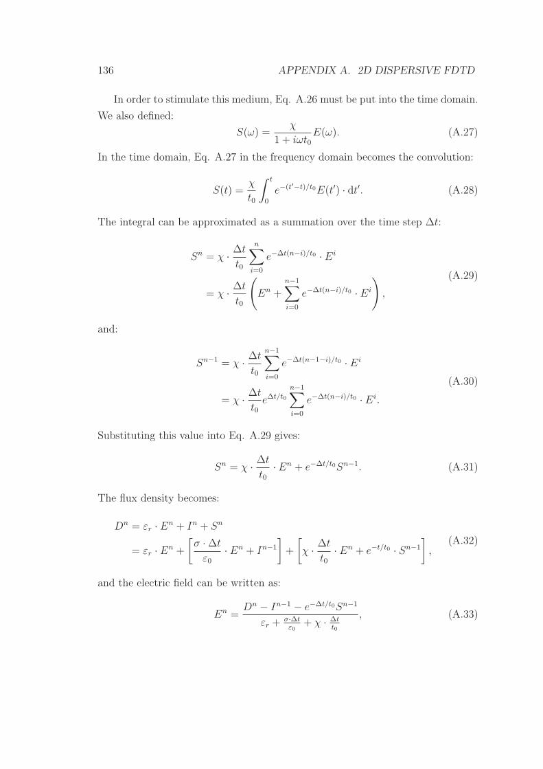
136 APPENDIX A. 2D DISPERSIVE FDTD
In order to stimulate this medium, Eq. A.26 must be put into the time domain.
We also defined:
S(ω) =χ
1 + iωt0E(ω). (A.27)
In the time domain, Eq. A.27 in the frequency domain becomes the convolution:
S(t) =χ
t0
∫ t
0
e−(t′−t)/t0E(t′) · dt′. (A.28)
The integral can be approximated as a summation over the time step ∆t:
Sn = χ · ∆t
t0
n∑
i=0
e−∆t(n−i)/t0 · Ei
= χ · ∆t
t0
(
En +n−1∑
i=0
e−∆t(n−i)/t0 · Ei
)
,
(A.29)
and:
Sn−1 = χ · ∆t
t0
n−1∑
i=0
e−∆t(n−1−i)/t0 · Ei
= χ · ∆t
t0e∆t/t0
n−1∑
i=0
e−∆t(n−i)/t0 · Ei.
(A.30)
Substituting this value into Eq. A.29 gives:
Sn = χ · ∆t
t0· En + e−∆t/t0Sn−1. (A.31)
The flux density becomes:
Dn = εr · En + In + Sn
= εr · En +
[
σ ·∆t
ε0· En + In−1
]
+
[
χ · ∆t
t0· En + e−t/t0 · Sn−1
]
,(A.32)
and the electric field can be written as:
En =Dn − In−1 − e−∆t/t0Sn−1
εr +σ·∆tε0
+ χ · ∆tt0
, (A.33)

137
with:
In = In−1 +σ ·∆t
ε0· En, (A.34)
Sn = e−∆t/t0Sn−1 + χ · ∆t
t0· En. (A.35)
However, another possibility, more powerful, is the use of the Z transforms
for the FDTD formulation of dispersive media [204]. We start again with the
calculation of E in a Debye media, in one dimension. We begin in the frequency
domain:
D(ω) =
(
εr +σ
iωε0+
χ
1 + iωt0
)
· E(ω). (A.36)
In the Z domain, the flux density becomes directly:
D(z) = εr · E(z) +σ ·∆t/ε01− z−1
· E(z) +χ ·∆t/t01 + z−1
· E(z). (A.37)
This equation can be rewritten as:
D(z) = εr · E(z) + z−1I(z) +σ ·∆t
ε0E(z) + e−∆t/t0z−1S(z) +
χ ·∆t
t0E(z), (A.38)
with:
I(z) =σ ·∆t/ε01− z−1
· E(z) = z−1I(z) +σ ·∆t
ε0E(z), (A.39)
S(z) =χ ·∆t/t0
1− e−∆t/t0z−1· E(z) = e−∆t/t0z−1S(z) +
χ∆t
t0E(z). (A.40)
The electric field is also:
E(z) =D(z)− z−1I(z)− e−∆t/t0z−1S(z)
εr +σ·∆tε0
+ χ · ∆tt0
. (A.41)
The advantage of the Z transforms is that the summation in the time domain
only consists in replacing, for example, E(z) by En or z−1E(z) by En−1. Moreover,
we get exactly the same expressions for En, In and Sn without doing anything to
the integrals and their approximations.

138 APPENDIX A. 2D DISPERSIVE FDTD
Metallic media
A metallic media can be implemented by starting with the Drude model for the
dielectric permittivity:
ε∗(ω) = 1−ω2p
ω(ω + iΓ), (A.42)
where Γ is the damping factor and ω2p the plasma frequency. The expression of the
permittivity can also be written as:
ε∗(ω) = 1ω2p/Γ
iω−
ω2p/Γ
Γ + iω. (A.43)
With the Z transforms, it becomes:
ε∗(z) =1
∆t+
ω2p/Γ
1− z−1−
ω2p/Γ
1− e−Γ·∆tz−1. (A.44)
The flux density is:
D(z) = ε∗(z) · E(z) ·∆t
= E(z) +ω2p∆t
Γ
[
(1− e−Γ·∆t)z−1
1− (1− e−Γ·∆t)z−1 + e−Γ·∆tz−2
]
E(z).(A.45)
And the electric field is:
E(z) = D(z)− z−1S(z), (A.46)
S(z) = (1− e−Γ·∆t)z−1S(z)− e−Γ·∆tz−2 +ω2p∆t
Γ(1− e−Γ·∆t)E(z), (A.47)
with:
S(z) =ω2p∆t
Γ
[
(1− e−Γ·∆t)
1− (1− e−Γ·∆t)z−1 + e−Γ·∆tz−2
]
E(z). (A.48)
The differential equations are written similarly to Eqs. A.11, A.12 and A.13.
Properties of the source wave
Next, we present the properties of the source wave we used. First, the temporal
confinement of the source wave can be obtained with a gaussian beam of the form:
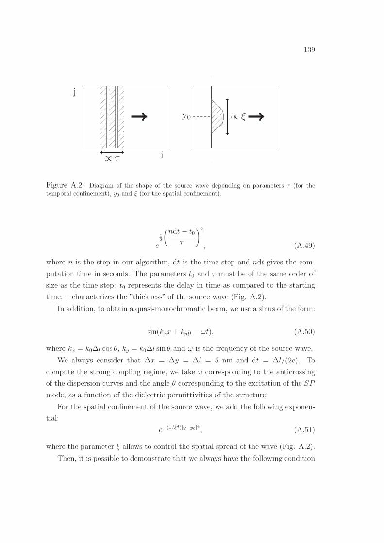
139
∝ ξy0
j
i∝ τ
Figure A.2: Diagram of the shape of the source wave depending on parameters τ (for thetemporal confinement), y0 and ξ (for the spatial confinement).
e
1
2
ndt− t0τ
2
, (A.49)
where n is the step in our algorithm, dt is the time step and ndt gives the com-
putation time in seconds. The parameters t0 and τ must be of the same order of
size as the time step: t0 represents the delay in time as compared to the starting
time; τ characterizes the ”thickness” of the source wave (Fig. A.2).
In addition, to obtain a quasi-monochromatic beam, we use a sinus of the form:
sin(kxx+ kyy − ωt), (A.50)
where kx = k0∆l cos θ, ky = k0∆l sin θ and ω is the frequency of the source wave.
We always consider that ∆x = ∆y = ∆l = 5 nm and dt = ∆l/(2c). To
compute the strong coupling regime, we take ω corresponding to the anticrossing
of the dispersion curves and the angle θ corresponding to the excitation of the SP
mode, as a function of the dielectric permittivities of the structure.
For the spatial confinement of the source wave, we add the following exponen-
tial:
e−(1/ξ4)[y−y0]4 , (A.51)
where the parameter ξ allows to control the spatial spread of the wave (Fig. A.2).
Then, it is possible to demonstrate that we always have the following condition

140 APPENDIX A. 2D DISPERSIVE FDTD
to compute a source wave:
λ ≥ 10∆l. (A.52)
Thus, the maximal frequency is fmax = c/(10∆l). This frequency gives the maxi-
mal value for which the fourier transformation of the incident field has to be equal
to zero. It is equivalent to say that we need ”enough sinus” in the envelope con-
taining the incident field to have a quasi-monochromatic incident beam (around
the frequency ω).

Appendix B
Resume en francais
Ces dernieres annees, les domaines de la communication, imagerie ou stockage
de donnees ont necessite l’utilisation de structures et composants toujours plus
petits. La micro-optique et plus particulierement la nanophotonique ont permis
ces etudes [1]. En effet, les guides d’onde usuels sont astreints a une taille minimale
regie par la limite de diffraction, λ/(2n), n etant l’indice du milieu optique et λ
la longueur d’onde de l’onde incidente. Des guides d’onde bases sur l’utilisation
des plasmons de surface permettent de confiner des ondes dans des structures sub-
longueur d’onde toujours plus petites. La branche de la nanophotonique attache
a l’etude de ces plasmons de surface est la plasmonique.
Les plasmons de surface (SP ) sont ainsi tres etudies actuellement [55] et sont
utilises dans la detection de molecules ou l’optique de surface. L’inconvenient
majeur de ces modes reside dans les pertes intrinseques au metal qui les carac-
terisent et limitent ainsi leur longueur de propagation [56, 57, 58, 59]. Plusieurs
pistes sont explorees pour diminuer l’effet de ces pertes. La plus connue consiste
a coupler des SPs entre eux. En effet, lorsque un film metallique devient assez
fin, il devient possible de coupler les SPs qui vivent sur chaque interface. Deux
nouveaux sont ainsi crees dont un mode dit « long range » (LRSP ) qui est car-
acterise par une longueur de propagation superieure a celle du plasmon classique
[90]. Une technique plus recemment etudiee pour ameliorer la propagation du
SP est l’application de gain dans le milieu directement en contact avec la couche
metallique [182, 183]. Neanmoins, dans ce cas, l’augmentation de l’emission plas-
mon est restreinte a la profondeur de peau de ce mode de surface dans le milieu a
gain. Une derniere idee avancee consiste a considerer l’amplification de l’emission
141

142 APPENDIX B. RESUME EN FRANCAIS
plasmon telle que celle de la lumiere conventionnelle dans un laser. Ce type de
dispositif est donc appele, par analogie, SPASER (Surface Plasmon Amplification
by Stimulated Emission of Radiation) [185, 186].
Partant de ces resultats, cette these nous permet de presenter un nouveau
type de dispositif constitue d’un guide d’onde dielectrique au-dessus duquel nous
placerons un film metallique afin de permettre un couplage fort plasmon/mode
guide. L’introduction de gain dans cette structure permettra alors des resultats
tres encourageant dans la recherche de l’amplification de l’emission plasmon. Dans
cette optique, le premier chapitre presente tout d’abord les outils numeriques et
theoriques necessaires a la modelisation d’un milieu stratifie dans le cas de moes a
pertes tels que les plasmons. Le deuxieme chapitre mettra l’accent sur les plasmons
de surface et nous presenterons alors un montage inedit permettant d’obtenir un
mode LRSP sans le mode SRSP a la surface d’un milieu infiniment conducteur.
Nous presenterons les caracteristiques d’un couplage entre des guides dielectriques,
avec la theorie des modes couples mais aussi le modele simple d’oscillateurs couples
dans le troisieme chapitre. Les derniers resultats sur la PT symetrie seront aussi
presentes. Finalement, le dernier chapitre traitera du couplage fort et plus partic-
ulierement de la demonstration du couplage entre un plasmon et un mode guide.
L’introduction de gain lineaire dans la structure permettra de diminuer d’autant
plus les pertes du plasmon et d’obtenir des longueurs de propagation de l’ordre du
millimetre.
Determination des modes
On considere un milieu stratifie compose de N couches minces [34]. Il s’agit d’un
milieu lineaire, homogene, isotrope, avec une dependance en temps de la forme
e−iωt. En polarisation transverse magnetique (TM) dans le plan (x, y), le champ
magnetique s’ecrit H = H(x, y)ez, il satisfait l’equation de Helmholtz :
div(ε−1j ∇H) + k2
jH = 0, (B.1)
ou k2j = k2
0εj est le vecteur d’onde dans chaque couche j. Cette equation doit etre
resolue dans chaque couche en respectant les conditions aux limites. On note α
et βj les vecteurs d’onde dans les directions x et y, respectivement. On peut alors

143
demontrer que la relation de dispersion correspond a :
α2 + β2j = k2
0εj, (B.2)
avec µr = 1. La determination de la quantite βj depend de α et kj :
βj =
√
k20εj − α2 if | α |< k0
√εj,
i√
α2 − k20εj if | α |> k0
√εj.
(B.3)
La premiere condition | α |< k0√εj implique que βj est reel et correspond a
des ondes propagatives. La seconde condition | α |> k0√εj implique que βj est
imaginaire et correspond a des ondes evanescentes. Ce type de solution correspond
a des ondes confinees a l’interface de deux milieux, ce qui est le cas des plasmons de
surface. La determination de ces solutions necessite donc un prolongement dans le
plan complexe et ne peut etre obtenu avec les techniques habituelles de resolution.
Nous allons utiliser le formalisme de la matrice S qui permet non seulement de
determiner les coefficients de reflexion et de transmission, R et T , mais aussi de
determiner tous les modes de la structure. Cette matrice permet de relier les
champs entrants I et I ′ de la structure aux champs sortants R et T .
On peut demontrer que les modes de la structure sont definis par l’existence
d’onde sortantes en l’absence d’excitation. Ainsi, pour chaque frequence ω, nous
devons trouver la constante de propagation α qui correspond a l’annulation du
determinant de la matrice S−1. Ceci est equivalent a trouver les poles de la ma-
trice S(ω, α). Neanmoins, la matrice S contient des variables complexes et la
determination de ses poles necessite une extension dans le plan complexe des solu-
tions pour α = (αR, αI). La methode employee implique l’utilisation des integrales
de Cauchy.
L’application de cette theorie a notre type de probleme est issue des travaux
de F. Zolla et al. [24]. La methode ainsi developpee est appelee la Tetrachotomie.
Cette methode permet de determiner les poles dans le plan complexe correspon-
dants a une fonction meromorphique f(α) dans C. En effet, si f(α) a un pole
unique au point α0, alors au voisinage de ce point il existe une fonction holomor-
phique non nulle G(α) (dans C \ α0) et la fonction f peut etre reecrite comme
[45] :
f(α) =G(α)
α− α0
. (B.4)

144 APPENDIX B. RESUME EN FRANCAIS
Considerons un lacet de Jordan Γ qui contient ce pole α0. De plus, on suppose
que le pole α0 est simple et que G n’a pas de pole a α = 0, on peut alors ecrire
que G(α) = αF (α) avec F une fonction holomorphique. Les integrales suivantes
permettent alors de determiner le pole α0 :
I0 =1
2iπ
∫
Γ
f(α)
αdα =
1
2iπ
∫
Γ
F (α)
α− α0
dα, (B.5)
I1 =1
2iπ
∫
Γ
f(α)dα =1
2iπ
∫
Γ
αF (α)
α− α0
dα, (B.6)
I2 =1
2iπ
∫
Γ
αf(α)dα =1
2iπ
∫
Γ
α2 F (α)
α− α0
dα. (B.7)
En effet, on peut demontrer qu’on a les relations suivantes :
α0 =I2I1
=I1I0. (B.8)
Ceci correspond a une application directe s’il n’existe qu’un seul pole. Considerons
desormais que la fonction f dans C a un nombre inconnu de poles αi dans
le plan complexe. La Tetrachotomie permet de determiner la valeur de chaque
pole (Fig. B.1). Le premiere etape consiste a isoler les poles les uns des autres.
L’evaluation des integrales I0, I1 et I2 permet de savoir s’il y a un pole, plusieurs
poles ou zero poles dans le rectangle Γ. Ensuite, dans le cas ou il y a plusieurs
poles (I2/I1 6= I1/I0), le rectangle Γ est divise en quatre nouveaux rectangles Γi
(i = [1, 2, 3, 4]), et de repeter le processus jusqu’a temps que tous les poles soient
isoles les uns des autres. On peut alors demontrer que l’efficacite de la methode
est de l’ordre de O( 1N4 ) avec N le nombre de rectangle necessaires pour isoler
l’ensemble des poles.
Couplage de plasmons de surface
Les plasmons de surface sont actuellement largement etudies et utilises dans de
nombreuses applications [55] grace a leur capacite a confiner la lumiere a des echelle
sub-longueur d’onde. Ce sont des ondes de surface qui se propagent typiquement
a l’interface entre un milieu dielectrique et un milieu metallique, ils correspondent
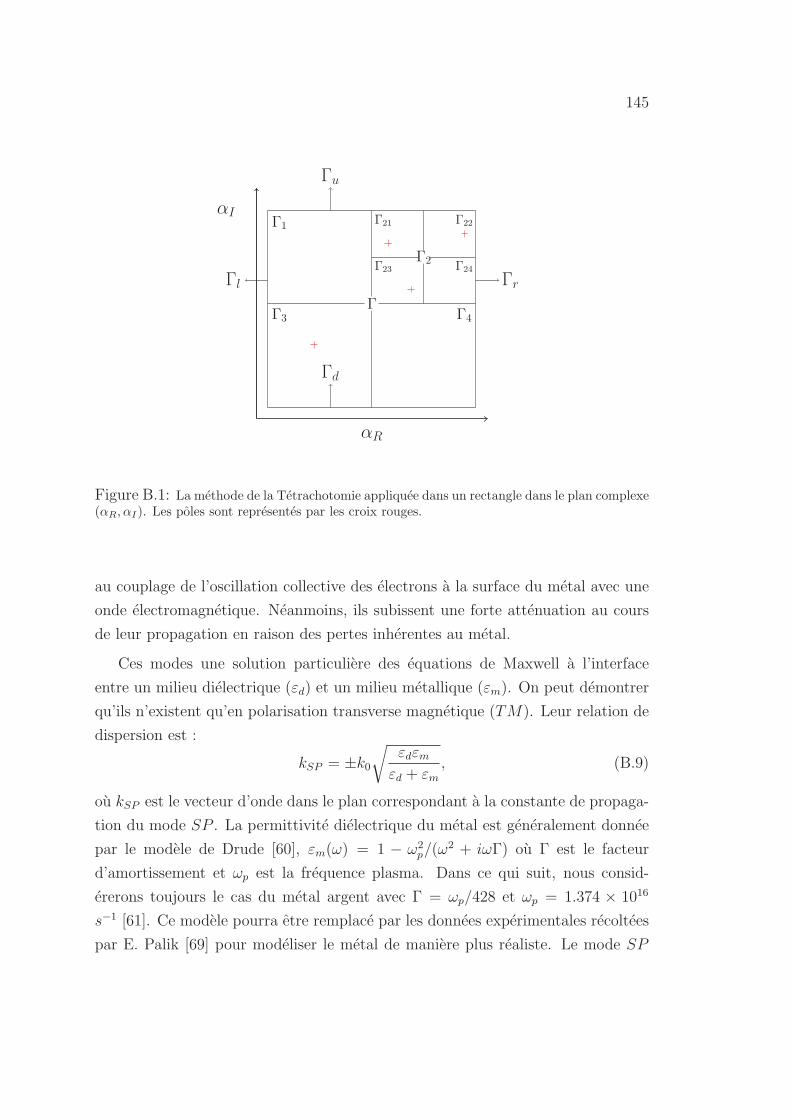
145
Γu
αR
αIΓ21
Γ
Γd
Γl
Γ2
Γ4
Γ1
Γ3
Γ22
Γ23 Γ24
Γr
Figure B.1: La methode de la Tetrachotomie appliquee dans un rectangle dans le plan complexe(αR, αI). Les poles sont representes par les croix rouges.
au couplage de l’oscillation collective des electrons a la surface du metal avec une
onde electromagnetique. Neanmoins, ils subissent une forte attenuation au cours
de leur propagation en raison des pertes inherentes au metal.
Ces modes une solution particuliere des equations de Maxwell a l’interface
entre un milieu dielectrique (εd) et un milieu metallique (εm). On peut demontrer
qu’ils n’existent qu’en polarisation transverse magnetique (TM). Leur relation de
dispersion est :
kSP = ±k0
√
εdεmεd + εm
, (B.9)
ou kSP est le vecteur d’onde dans le plan correspondant a la constante de propaga-
tion du mode SP . La permittivite dielectrique du metal est generalement donnee
par le modele de Drude [60], εm(ω) = 1 − ω2p/(ω
2 + iωΓ) ou Γ est le facteur
d’amortissement et ωp est la frequence plasma. Dans ce qui suit, nous consid-
ererons toujours le cas du metal argent avec Γ = ωp/428 et ωp = 1.374 × 10¹⁶
s−1 [61]. Ce modele pourra etre remplace par les donnees experimentales recoltees
par E. Palik [69] pour modeliser le metal de maniere plus realiste. Le mode SP

146 APPENDIX B. RESUME EN FRANCAIS
0 2
1
α c / ωp
ω /
ωp
ω = k0 sqrt(ε
d) cω = k
0 c
coupling
Figure B.2: Dans l’air, ω = k0c, tandis que dans un dielectrique (εd > 1), ω = k0√εdc = kxi c.
La composante dans le plan du vecteur d’onde kxi devient superieur a k0. Il existe alors unefrequence pour laquelle kxi = kSP et le couplage avec le mode SP devient possible a l’interfacemetal/air.
etant un mode non radiatif, sa courbe de dispersion se situe toujours en dessous
du cone de lumiere defini par le milieu d’incidence. Il est necessaire d’employer
des montages particuliers pour pouvoir l’exciter, le plus utilise d’entre eux etant
le montage ATR (Attenuated Total Reflection) initie par E. Kretschmann [5]. Ce
montage consiste en un prisme de verre sur lequel est accole une couche metallique
d’epaisseur determinee. L’excitation plasmon sera dependante de l’angle θi de
l’onde incidente dans le verre et de l’epaisseur de la couche metallique. Dans le
visible, les donnees typiques pour obtenir cette excitation sont les suivantes : une
longueur d’onde λ = 632.8 nm pour le champ incident, les permittivites εd = 2.25
(verre) pour le prisme, εa = 1 (air) en sortie en dessous du metal et εm pour le
metal deduit des donnees Palik [69] pour l’argent. Le plasmon est ainsi excite
dans l’air pour un angle d’incidence θi = 43.7 avec un film metallique d’epaisseur
em = 45 nm.
Le montage ATR permet d’abaisser le cone de lumiere du milieu d’incidence
et de permettre l’excitation du plasmon par une onde incidente dans un milieu
dielectrique (εd > 1) de l’autre cote du film metallique dans un milieu d’incice
inferieur (comme l’air). On a en effet ω = k0√εdc = kx
i c dans le milieu dielectrique
ce qui rend possible de trouver une frequence pour laquelle kxi = kSP (Fig. B.2).
Le couplage de deux SP existants de part et d’autre d’un film metallique suff-

147
isamment fin (en dessous de 50 nm [80]) dans un milieu symetrique constitue une
premiere possibilite pour ameliorer leur propagation. Cette configuration permet
la creation de deux nouveaux sont ainsi crees un mode dit « long range » (LRSP )
qui est caracterise par une longueur de propagation superieure a celle du plas-
mon classique et un mode dit « short range » (SRSP ) qui aura une longueur de
propagation inferieure, la difference entre les deux modes etant la symetrie de leur
champ correspondant dans le film metallique [90]. Leurs relations de dispersion
s’obtiennent aussi a partir des equations de Maxwell :
ω+: βdεm + βmεd tanh
(
βmem2
)
= 0, (B.10)
ω−: βdεm + βmεd coth
(
βmem2
)
= 0, (B.11)
avec la relation α2 + β2d,m = k2
0εd,m.
Le mode interessant a privilegier est le mode LRSP qui peut, par exemple, avoir
une longueur de propagation 27 fois superieure a celle d’un mode SP [91,92] dans
certaines conditions. Nous proposons donc un montage permettant l’excitation de
ce mode directement dans un milieu sans necessite d’avoir un milieu symetrique
(contrainte importante pour des utilisations pratiques) et sans excitation du mode
SRSP . En effet, nous pouvons demontrer l’equivalence entre un montage constitue
d’un film metallique d’epaisseur em dans un milieu dielectrique symetrique et un
montage consistant en une couche metallique d’epaisseur em/2 depose sur un milieu
infiniment conducteur (Fig. B.3). Cette demonstration grace a la theorie des
images qui permet de rendre equivalent une charge +q place a une distance d d’un
milieu infiniment conducteur avec un systeme constitue de deux charges, disposees
a une distance deux fois d [105]. Ainsi, pour avoir des montages equivalent dans
notre cas, il faut bien considerer une epaisseur pour la couche metallique deposee
a la surface du milieu infiniment conducteur deux fois moins importante que le
montage de depart.
La resolution des equations de Maxwell pour le montage Fig. B.3b avec les
bonnes conditions aux limites nous apporte une relation de dispersion pour le
mode existant a l’interface metal/dielectrique absolument equivalente a celle du
mode LRSP (Eq. B.10). On peut alors tracer les differentes courbes de dispersion
obtenues par Tetrachotomie (Fig. B.4).

148 APPENDIX B. RESUME EN FRANCAIS
em
x
εd
y
εm
εd
(a)
em/2
x
εd
y
εm
PEC
(b)
Figure B.3: (a) Film metallique (εm) d’epaisseur em dans un milieu dielectrique (εd)symetrique. (b) Film metallique (εm) d’epaisseur em/2 depose sur un milieu infiniment con-ducteur dans un milieu dielectrique (εd).
0 0.1 0.2 0.3 0.4 0.50.2
0.4
0.6
0.8
1
ω /
ωp
α ( nm−1
)
ω+
ω−
Figure B.4: Les carres noirs representent les courbes de dispersion ω+ du mode LRSP et ω− dumode SRSP pour un film metallique d’epaisseur em = 30 nm. Les carres rouges representent lacourbe de dispersion du mode existant a l’interface metal/dielectrique dans le montage constitued’une couche metallique depose sur un milieu infiniment conducteur dans un milieu dilectrique(Fig. B.3b).

149
Couplage de guides dielectriques
Les guides d’onde dielectriques constituent un modele simple pour etudier le les me-
canismes de confinement et la propagation des ondes dans des montages optiques.
En fonction de l’epaisseur du guide, la forme des modes qui se propagent peuvent
etre determinee en fonction des permittivites dielectriques du guide d’onde. Le
couplage de deux guides dielectriques identiques a ete largement etudie au cours
des dernieres decennies, notamment a l’aide de la theorie des modes couples [25,
26, 27, 28, 29]. Cette theorie est basee sur le fait de considerer le champ comme
une superposition lineaire des modes existants dans la structure.
Si on considere deux guides dielectriques suffisamment proches pour interagir,
le champ total du systeme peut s’ecrire comme une superposition lineaire des
modes correspondants aux guides d’onde pris individuellement. La conservation
en energie permet alors de determiner les termes de couplage reliant les amplitudes
des deux modes si on considere que ce couplage reste faible. On calcule alors les
transferts de puissance entre les deux modes, soit en fonction du temps, soit en
fonction de la distance parcourue parallelement aux guides. Cette theorie est
toujours presentee en polarisation transverse electrique (TE). Nous presentons ici
une possibilite de l’obtenir en polarisation TM .
Pour ecrire la theorie des modes couples en polarisation TM , il est necessaire
de considerer une forme linearisee des equations de Maxwell pour les deux guides
1 et 2 :
div(χ1) = −k20u1, ∇u1 = ε1χ1,
div(χ2) = −k20u2, ∇u2 = ε2χ2.
(B.12)
On rappelle que sous cette forme, les equations de Maxwell en polarisation TE
seraient div(χ) = −k20εu et ∇u = χ. Les solutions sont alors recherchees avec
l’ansatz :
(u, χ) = a1(z)(u1, χ1) + a2(z)(u2, χ2). (B.13)
On demontre alors que les solutions sont de la forme Apeiγz (p = 1, 2) avec les
deux valeurs propres γ = Υ± Γ ou :
Γ =
√
Υ2 − t1t21− | R |2 , (B.14)

150 APPENDIX B. RESUME EN FRANCAIS
n0 +∆n+ i∆αλ/(2π)
z
Re[n(x)] Im[n(x)]
n0 +∆n − i∆αλ/(2π)
n0
n0
n0
x
Figure B.5: Deux guides d’onde couples avec un ajout de gain dans l’un (avec un partie imag-inaire negative ajoutee a l’indice) et un ajout de pertes dans l’autre (avec une partie imaginairepositive ajoutee a l’indice) [120].
Υ =Rt2 −Rt12(1− | R |2) , (B.15)
avec les notations : δ1,2 = ε − ε1,2, ∆ = γ2 − γ1, R =∫
(υ1X2z − X1zυ2)dx, T =
X1zX2z, t2 =∫
δ2Tdx, t1 =∫
δ1Tdx, W1,2 =∫
δ1,2 | X1z,2z |2 dx, P1,2 =∫
P1z,2zdz.
Un cas particulier du couplage de deux guides optiques est celui ou les guides
respectent la PT symetrie (Parity Time). Cette symetrie a ete mise en evidence
en mecanique quantique par C. M. Bender [30] et a ensuite ete etendue au cas de
montages optiques. On considere ainsi deux guides optiques couples. Du gain est
ajoute dans l’un et des pertes (parfaitement equivalentes) sont ajoutes dans l’autre
(Fig. B.5). Le couplage sera a nouveau fonction de la distance qui separe les deux
guides. Apres s’etre place a une distance optimal, les valeurs gain/pertes sont
augmentees jusqu’a atteindre un certain seuil dans le comportement des guides.
On observe une brisure spontanee de la symetrie a partir de laquelle les constantes
de propagation des guides deviennent complexe conjuguees l’une de l’autre (Fig.
B.6)[120].

151
0 2 4 6 8 10
13.378
13.3782
13.3784
13.3786
13.3788
13.379
∆α (cm−1
)
kz (
µm
−1 )
Figure B.6: Les constantes de propagation kz des modes guides en fonction du parametre ∆α.Les constantes de propagation se rapprochent l’une de l’autre jusqu’a atteindre un point critique∆αc ∼ 8.4 [120]. Apres ce point, les constantes de propagation deviennent complexe conjugueesl’un de l’autre et une brisure spontanee de la PT symetrie est observee.
Couplage fort entre plasmons de surface et modes
guides
Lorsque l’interaction entre mode electromagnetique et un emetteur augmente, le
regime de couplage fort peut apparaıtre. Ce regime a beaucoup ete etudie dans les
microcavites depuis les travaux de C. Weisbuch et al. [31]. Dans une microcavite
dans ce regime, l’emission spontanee irreversible est remplacee par un echange
reversible d’energie entre le mode electromagnetique et l’emetteur. Le regime de
couplage fort se caracterise par un anticroisement des courbes de dispersion associe
a un croisement des courbes d’absorption pour la meme valeur de la constante
de propagation. Cet anticroisement se caracterise par une energie de Rabi [33].
L’echange d’energie est periodique avec une echelle de temps inferieure a l’inverse
du taux de desexcitation de la cavite. Ce regime de couplage fort a aussi ete
demontre entre un plasmon et un exciton par J. Bellessa et al. [162, 174, 176].
Le present travail se propose de demontrer la possibilite d’obtenir un couplage
fort entre un plasmon et un mode guide. Le montage utilise est presente dans
la figure B.7. Il est constitue d’un guide d’onde dielectrique constitue d’un coeur
d’epaisseur 130 nm de SiO2 (εg = 4.84) entoure de T iO2 (εd = 2.1025) [184],
un film metallique est place au-dessus du guide d’epaisseur em = 45 nm avec un

152 APPENDIX B. RESUME EN FRANCAIS
GM
SPd
SPuεt
eg
εm
εd
εg
ed
εd x0
em
y
Figure B.7: Structure guidante plane qui permet le couplage fort entre le plasmon de surfaceSPd et le mode guide GM . Les permittivites dielectriques de chaque couche sont εd = 2.1025,εg = 4.84, εt = 3, et εm. Les epaisseurs du coeur du guide est eg et du film metallique est em sontfixees. Seule l’epaisseur ed, la distance entre les deux modes couples, est modifiee pour obtenirle regime de couplage fort.
milieu dielectrique de permittivite dielectrique (εt = 3) superieur a celle du guide
pour que le plasmon superieur ait une courbe de dispersion en dessous du cone de
lumiere correspondant a εd.
Le mode guide GM est considere comme monomode avec ces parametres. Le
plasmon en contact avec le guide d’onde est note SPd et l’autre est note SPu.
Le regime de couplage fort va etre demontre entre les modes SPd et GM en
fonction de l’epaisseur ed. Pour trouver l’epaisseur optimale, on fait varier cette
derniere jusqu’a obtenir le croisement des parties imaginaires de la constante de
propagation. Ces dernieres correspondent aux pertes inherentes aux modes de la
structure. Le croisement intervient pour une meme constante de propagation que
l’anticroisement des courbes de dispersion αR = 0.028 nm−1 lorsque em = 100 nm
pour une longueur d’onde λ = 421.5 nm.
La figure B.8a represente les courbes de dispersion. En rouge et bleu, les
courbes correspondant aux modes avant tout couplage, pour lesquelles on observe
un croisement. L’anticroisement des courbes pour le montage complet est une
signature du regime de couplage fort. Les nouveaux modes ainsi crees sont des
modes hybrides des modes initiaux, notes GMc et SPd,c. L’energie de Rabi est

153
0.02 0.03 0.04 0.05
0.2
0.25
0.3
0.35
0.4
αR
( nm−1
)
ω /
ωp
complete device
GM mode
SPP modes
(a)
0 5 10 15 20
x 10−4
0.25
0.3
0.35
0.4
αI ( nm
−1 )
ω /
ωp
complete device
GM mode
SPP modes
(b)
Figure B.8: (a) Courbes de dispersion et (b) courbes d’absorption lorsque ed = 100 nm,l’epaisseur optimale pour obtenir le regime de couplage fort : la frequence ω, normalisee a lafrequence plasma ωp, est tracee en fonction de la constante de propagation αR et sa partieimaginaire αI , respectivement. L’anticroisement des courbes de dispersion et le croisement descourbes d’absorption pour la meme valeur de la constante de propagation est caracteristique duregime de couplage entre les modes GM et SPd.
ER = 134 meV.
La figure B.8b represente les courbes d’absorption obtenues grace a la methode
de la Tetrachotomie et qui caracterisent les pertes intrinseques de chaque mode.
Le croisement des courbes d’absorption pour la meme valeur de la constante de
propagation est une caracteristique du regime de couplage fort entre les modes
GM et SPd. Le mode GM echange de l’energie avec le mode SPd et voit ses
pertes augmenter tandis que celles du plasmon diminuent par rapport aux courbes
en rouge et bleu correspondantes a l’absorption avec le couplage.
Grace a la FDTD, on peut alors observer des oscillations temporelles entre les
deux modes avec une periode Tt = 30.7 fs mais aussi des oscillations spatiales grace
au confinement du faisceau incident sur une gamme de la constante de propagation
reduite a l’anticroisement avec une periode Ts = 1.7µm. On peut aussi tracer la
longueur de propagation des modes en fonction de la distance ed. On observe alors
que la longueur de propagation du mode SPd fait plus que doubler en regime de
couplage fort en passant de 400 nm a 1036 nm. Par ailleurs, le confinement du
mode hybride SPd,c est de l’ordre de 50 nm, ce qui est un tres bon confinement
pour un mode de surface.
Une remarque importante concerne la longueur d’onde choisie au niveau de

154 APPENDIX B. RESUME EN FRANCAIS
l’anticroisement. Dans la figure B.8a, on note qu’on peut definir deux valeurs
correspondantes chacune a l’une des deux courbes a l’anticroisement. En tracant
les cartes de champs, nous pouvons observer que la courbe haute (λh = 405 nm)
correspond d’avantage au mode hybride GMc tandis que la courbe basse (λl =
421.5 nm) correspond au mode hybride SPd,c. Notons par ailleurs que l’epaisseur
optimale ed pour λh devient 110 nm au lieu de 100 nm. Dans la suite, nous
allons ajouter du gain lineaire au sein de notre structure en distinguant ces deux
possibilites.
On commence par injecter du gain directement dans le coeur du guide, de la
forme εg = 4.84 − i ∗ gn avec un gain normalise gn = (λ/2 ∗ pi)g par rapport au
gain g qui sera de l’ordre du nanometre. En tracant la longueur de propagation
en fonction du gain pour chacune des longueurs d’onde λh et λl, on observe deux
pics tres marques correspondants aux deux modes qu’on peut identifier grace aux
cartes de champs. On observe alors que la longueur de propagation du mode
hybride SPd,c est multiplie par 16 a λl mais reste tres inferieure a celle du mode
hybride GM quelque soit la longueur d’onde et l’epaisseur du guide associee.
On injecte alors du gain dans la couche intermediaire entre les deux modes
couples, εd = 2.1025− i∗gn. En tracant la longueur de propagation en fonction du
gain, on observe cette fois une augmentation superieure de celle correspondante
au mode hybride SPd,c par rapport a celle du mode hybride GMc. On obtient
ainsi une longueur finale de propagation pour le mode hybride SPd,c egale a 6.5
mm pour un gain g = 1.5 nm ce qui represente une augmentation considerable par
rapport au mode non couple.
En retirant le coeur du guide d’onde, il n’y a plus de regime de couplage fort et
on observe que l’augmentation de la longueur de propagation reste bien inferieure
a celle avec le couplage fort. Nous concluons sur l’interet que ce montage peut
apporter pour la realisation d’un montage permettant l’amplification du mode
plasmon tel que les SPASER.

Appendix C
Abstract in English
Surface plasmon polaritons are non radiative modes which exist at the interface
between a dielectric and a metal. They can confine light at sub-wavelength scales.
However, their propagation is restricted by the intrinsic losses of the metal which
imply a rapid absorption of the mode. The aim of this thesis is the study of
the coupling of surface plasmons in metallo-dielectric planar structures. The first
solution to solve the problem of propagation of the surface plasmons consists in
coupling these modes to one another. In a symmetric medium, when the thickness
of the metallic film becomes thin enough, the coupling between the plasmon modes
which exist on each side becomes possible. One of the coupled modes which is cre-
ated, the so-called long range surface plasmon, has a bigger propagation length
than the usual plasmon. We present a configuration which allows its excitation
without the short range mode with a metallic layer deposited on a perfect electric
conductor substrate. This excitation can be done in air and allows applications,
such as the detection and the characterisation of molecules. Then, we present the
coupling between dielectric waveguides, and, in particular, the coupled-mode the-
ory in the case of the transverse magnetic polarisation. We consider also the case
of PT symmetric structure. The last part of this work presents the demonstration
of the strong coupling regime between a surface plasmon and a guided mode. We
demonstrate an increase of the propagation length of the hybrid surface plasmon,
which still has the confinement of a surface mode. Adding linear gain in the layer
between both coupled modes allows an enhancement of the propagation lengths
of the modes, and more precisely of the hybrid surface plasmon mode, which can
propagate at the millimeter scale.
155

156 APPENDIX C. ABSTRACT IN ENGLISH

Bibliography
[1] M. I. Stockman, “Nanophotonics : The physics behind the applications,” Phys. Today,vol. 64, p. 39, 2011.
[2] R. W. Wood, “On a remarkable case of uneven distribution of light in a diffraction gratingspectrum,” Philos. Mag., vol. 4, p. 396, 1902.
[3] R. H. Ritchie, “Plasma losses by fast electrons in thin films,” Phys. Rev., vol. 106, no. 5,p. 874, 1957.
[4] C. J. Powell and J. B. Swan, “Effect of oxidation of the characteristic loss spectra ofaluminium and magnesium,” Phys. Rev., vol. 118, p. 640, 1960.
[5] H. Raether, Surface plasmons on smooth and rough surface and on gratings. Berlin:Springer-Verlag, 1988.
[6] U. C. Fischer and D. W. Pohl, “Observation of single-particle plasmons by near-field opticalmicroscopy,” Phys. Rev. Lett., vol. 62, p. 458, 1989.
[7] P. Dawson, F. de Fornel, and J.-P. Goudonnet, “Imaging of surface plasmon propagationand edge interaction using a photon scanning tunneling microscope,” Phys. Rev. Lett.,vol. 72, no. 18, p. 2927, 1994.
[8] R. Yang and Z. Lu, “Subwavelength plasmonic waveguides and plasmonic materials,” In-
tern. J. of Opt., vol. 2012, p. 258013, 2012.
[9] Z. Hans and S. I. Bozhevolnyi, “Radiation guiding with surface plasmon polaritons,”Rep.Prog. Phys., vol. 76, p. 016402, 2013.
[10] S. A. Maier and H. A. Atwater, “Plasmonics : localization and guiding of electromagneticenergy in metal/dielectric strutures,” J. oj Appl. Phys., vol. 98, p. 011101, 2005.
[11] A. V. Zayats and I. I. Smolyaninov, “Near-field photonics : surface plasmon polaritons andlocalized surface plasmons,” J. Opt. A: Pure Appl. Opt., vol. 5, p. S16, 2003.
[12] W. L. Barnes, A. Dereux, and T. W. Ebbesen, “Surface plasmon subwavelength optics,”Nature, vol. 424, p. 824, 2003.
[13] A. V. Zayats, I. I. Smolyaninov, and A. A. Maradudin, “Nano-optics of surface plasmonpolaritons,” Phys. Rep., vol. 408, p. 131, 2005.
[14] T. W. Ebbesen, H. J. Lezec, H. F. Ghaemi, T. Thio, and P. A. Wolff, “Extraordinaryoptical transmission through sub-wavelength hole arrays,”Nature, vol. 391, p. 667, 1998.
[15] H. A. Bethe, “Theory of diffraction by small holes,” Phys. Rev., vol. 66, p. 163, 1944.
[16] Y. Fu and X. Zhou, “Plasmonic lenses : a review,” Plasmonics, vol. 5, p. 287, 2010.
[17] J. B. Pendry, “Negative refraction makes a perfect lens,”Phys. Rev. Lett., vol. 85, p. 3966,2000.
157

158 BIBLIOGRAPHY
[18] N. Fang, H. Lee, C. Sun, and X. Zhang, “Sub-diffraction optical imaging with a silversuperlens,” Science, vol. 308, p. 534, 2005.
[19] J. Vickovic and M. Loncar, “Surface plasmon enhanced light-emitting diode,”Quant. Elec-
tron., vol. 36, no. 10, p. 1131, 2000.
[20] H. A. Atwater and A. Polman, “Plasmonics for improved photovoltaic devices,” Nature
Mat., vol. 9, p. 205, 2010.
[21] R. J. C. Brown and M. J. T. Milton, “Nanostructures and nanostructured substrates forsurface-enhanced raman scattering (sers),” J. of Raman Spectrosc., vol. 39, p. 1313, 2008.
[22] K. Thyagarajan, S. Rivier, A. Lovera, and O. J. F. Martin, “Enhanced second-harmonicgeneration from double resonant plasmonic antennae,” Opt. Express, vol. 20, p. 12860,2012.
[23] A. G. Brolo, “Plasmonics for future biosensors,”Nature Photon., vol. 6, p. 709, 2012.
[24] Y. Jiang, H.-Y. Wang, H. Wang, B.-R. Gao, Y.-W. Hao, Y. Jin, Q.-D. Chen, and H.-B.Sun, “Surface plasmon enhanced fluorescence of dye molecules on metal grating films,” J.Phys. Chem. C, vol. 115, no. 25, p. 12636, 2011.
[25] E. Fort and S. Gresillon, “Surface enhanced fluorescence,” Appl. Phys., vol. 41, no. 1,p. 013001, 2008.
[26] D. Schultz, “Plasmon resonant particles for biological detection,” Current opinion in
biotechnol., vol. 14, p. 13, 2003.
[27] A. V. Kabashin, P. Evans, S. Pastkovsky, W. Hendren, G. A. Wurtz, R. Atkinson, R. Pol-lard, V. A. Podolskiy, and A. V. Zayats, “Plasmonic nanorod metamaterials for biosensing,”Nature Mat., vol. 8, p. 867, 2009.
[28] S. Zhijun and K. Hongkoo,“Refractive transmission of light and beam shaping with metallicnano-optic lenses,”Appl. Phys. Lett., vol. 85, p. 642, 2004.
[29] M. I. Stockman, “Nanoplasmonics : past, present and glimpse into future,” Opt. Express,vol. 19, no. 22, p. 22029, 2011.
[30] E. Ozbay, “Plasmonics : merging photonics and electronics at nanoscale dimensions,” Sci-ence, vol. 311, p. 189, 2006.
[31] J. M. Pitarke, V. M. Silkin, E. V. Chulkov, and P. M. Echenique, “Theory of surfaceplasmons and surface-plasmon polaritons,”Rep. Prog. Phys., vol. 70, pp. 1–87, 2007.
[32] D. Sarid and W. Challener, Modern introduction to surface plasmons. Cambridge Univer-sity, 2010.
[33] K. Welford, “Surface plasmon-polariton and their uses,” Opt. and Quant. Elec., vol. 23,pp. 1–27, 1991.
[34] P. Berini, R. Charbonneau, N. Lahoud, and G. Mattiussi, “Characterization of long-rangesurface-plasmon-polariton waveguides,” J. Appl. Phys., vol. 98, p. 043109, 2005.
[35] S. Herminghaus, “Attenuated total reflectance as a quantum interference phenomenon,”Opt. Lett., vol. 19, no. 4, p. 293, 1994.
[36] P. Berini, “Long-range surface plasmon polaritons,”Advances in Opt. and Photonics, vol. 1,p. 484, 2009.
[37] D. Sarid, “Long-range surface-plasma waves on very thin metal films,” Phys. Rev. Lett.,vol. 47, p. 1927, 1981.

BIBLIOGRAPHY 159
[38] M. Miyata and J. Takahara, “Excitation control of long-range surface plasmons by twoincident beams,”Opt. Express, vol. 20, p. 9493, 2012.
[39] V. N. Konopsky and E. V. Alieva, “Long-range propagation of plasmon polaritons in athin metal film on a one-dimensional photonic crystal surface,” Phys. Rev. Lett., vol. 97,p. 253904, 2006.
[40] A. Yanai and U. Levy, “The role of short and long range surface plasmons for plasmonicfocusing applications,”Opt. Express, vol. 17, no. 16, p. 14270, 2009.
[41] S. Wuestner, A. Pusch, K. L. Tsakmakidis, J. M. Hamm, and O. Hess, “Overcoming losseswith gain in a negative index metamaterial,” Phys. Rev. Lett., vol. 105, p. 127401, 2010.
[42] O. Hess, J. B. Pendry, S. A. Maier, R. F. Oulton, J. M. Hamm, and K. L. Tsakmakidis,“Active nanoplasmonic metamaterials,”Nature Mat., vol. 11, p. 573, 2012.
[43] D. J. Bergman and M. I. Stockman, “Surface plasmon amplification by stimulated emissionradiation : quantum generation of coherent surface plasmons in nanosystems,”Phys. Rev.Lett., vol. 90, no. 2, p. 027402, 2003.
[44] M. A. Noginov, G. Zhu, A. M. Belgrave, R. Bakker, V. M. Shalaev, E. E. Narimanov,S. Stout, E. Herz, T. Suteewong, and U. Wiesner, “Demonstration of a spaser-basednanolaser,”Nature, vol. 460, p. 1110, 2009.
[45] C. Symonds, G. Lheureux, J. P. Hugonin, J. J. Greffet, J. Laverdant, G. Brucoli,A. Lemaıtre, P. Senellart, and J. Bellessa, “Confined tamm plasmon lasers,” Nano Lett.,vol. 13, no. 7, pp. 3179–3184, 2013.
[46] M. Kaliteevski, S. Brand, R. A. Abram, I. Iorsh, A. V. Kavokin, and I. A. Shelykh, “Hybridstates of tamm plasmons and exciton polaritons,” Appl. Phys. Lett., vol. 95, no. 251108,2009.
[47] M. E. Sasin, R. P. Seisyan, M. A. Kaliteevski, S. Brand, R. A. Abram, J. M. Chamber-lain, I. V. Iorsh, I. A. Shelykh, A. Y. Egorov, A. P. Vasil’ev, V. S. Mikhrin, and A. V.Kavokin, “Tamm plasmon-polaritons: First experimental observation,” Superlattices and
Microstructures, vol. 47, pp. 44–49, 2010.
[48] F. Zolla, G. Renversez, A. Nicolet, B. Kuhlmey, S. Guenneau, and D. Felbacq, Foundationsof photonic crystal fibres. Imperial College Press, 2005.
[49] A. Yariv, “Universal relations for coupling of optical power between microresonators anddielectric waveguides,” Electronics Lett., vol. 36, no. 4, pp. 321–322, 2000.
[50] A. Yariv, “Coupled-mode theory for guided-wave optics,” IEEE J. of Quantum Electron.,vol. QE-9, no. 9, p. 919, 1973.
[51] S. L. Chuang, Physics of optoelectronic devices. John Wiley and Sons Inc., 1995.
[52] H. A. Haus, “Coupled-mode theory,” Proc. of the IEEE, vol. 79, 1991.
[53] H. A. Haus, W. P. Huang, S. Kawakami, and N. A. Whitaker, “Coupled-mode theory ofoptical waveguides,” J. of Lighwave Techno., vol. LT-5, no. 1, p. 16, 1987.
[54] C. M. Bender, “Real spectra in non-hermitian hamiltonian having pt symmetry,” Phys.
Rev. Lett., vol. 80, no. 24, p. 5243, 1998.
[55] C. Weisbuch, M. Nishioka, A. Ishikawa, and Y. Arakawa, “Observation of the coupledexciton-photon mide splitting in a semiconductor quantum microcavity,”Phys. Rev. Lett.,vol. 69, no. 23, p. 3314, 1992.

160 BIBLIOGRAPHY
[56] B. Gayral and P. Senellart, “Controle de l’emission spontanee d’un emetteur a l’etat solide,”Images de la Physique, 2007.
[57] T. J. Davis, “Surface plasmon modes in multi-layer thin-films,” Opt. Comm., vol. 282,p. 135, 2009.
[58] D. K. Ko and J. R. Sambles, “Scattering matrix method for propagation of radiation instratified media : attenuated total reflection studies of liquid crystals,” J. Opt. Soc. Am.
A, vol. 5, no. 11, p. 1863, 1988.
[59] A. Tishchenko,“Fenomenological representation of deep and high contrast lamellar gratingsby means of the modal method,”Opt. and Quant. Elec., vol. 37, p. 309, 2005.
[60] D. A. Bykov and L. L. Doskolovich, “Numerical methods for calculating poles of the scat-tering matrix with applications in grating theory,” J. of Lighwave Techno., vol. 31, no. 5,p. 793, 2013.
[61] G. Gallatin, J. C. Webster, E. C. Kintner, and C. J. Morgan, “Scattering matrices forimaging layered media,” J. Opt. Soc. Am. A, vol. 5, no. 2, p. 220, 1988.
[62] C. C. Katsidis and D. I. Siapkas, “General transfer-matrix method for optical multilayersystems with coherent, partially coherent, and incoherent interference,”Appl. Opt., vol. 41,no. 19, p. 3978, 2002.
[63] Z.-Y. Li, “Principles of the plane-wave transfer-matrix method for photonic crystals,” Sci.Technol. Adv. Mater., vol. 6, p. 837, 2005.
[64] H. T. Minden, “Scatter matrix algorithm for the transverse kerr magnetooptic effect inmultilayer optical film structures,”Appl. Opt., vol. 29, no. 27, p. 3955, 1990.
[65] O. Buccafusca, “The mathematical group of scattering matrices: Introduction of scatteringmatrix multiplication,”Microw. Opt. Technol. Lett., vol. 49, pp. 179–183, 2007.
[66] M. Neviere, E. Popov, and R. Reinisch,“Electromagnetic resonances in linear and nonlinearoptics : phenomenological study of grating behavior through the poles and zeros of thescattering operator,” J. Opt. Soc. Am. A, vol. 12, no. 3, p. 513, 1995.
[67] G. J. Gbur, Mathematical methods for optical sciences, vol. chapter 9. Cambridge Univer-sity, 2011.
[68] R. Petit, L’outil mathematique. Masson, 3rd ed. ed., 1991.
[69] P. Helluy, S. Maire, and P. Ravel, “Integration numerique d’ordre eleve de fonctionsregulieres ou singulieres sur un intervalle,” C. R. Acad. Sci. Paris, vol. 327, pp. 843–848,1998.
[70] F. Jedrzejewski, Introduction aux methodes numeriques. Springer-Verlag, 2nd ed., 2005.
[71] L. Novotny and B. Hecht, Principles of nano-optics. Cambridge University, 2nd ed. ed.,2012.
[72] P. Drude, “Zur elektronentheorie der metalle,”Annalen der Physik, vol. 306, no. 3, pp. 566–613, 1900.
[73] E. J. Zeman and G. C. Schatz, “An accurate electromagnetic theory study of surfaceenhancement factors for silver, gold, copper, lithium, sodium, aluminum, gallium, indium,zinc, and cadmium,” J. Phys. Chem., vol. 91, pp. 634–643, 1987.
[74] B. Ong, X. Yuan, S. Tjin, and J. Zhang, “Optimised fild thickness for maximum evanescentfield enhancement of a bimetallic film surface plasmon resonance biosensor,” Sensors and
Actu. B, vol. 114, pp. 1028–1034, 2006.

BIBLIOGRAPHY 161
[75] M. Watanabe and K. Kajikawa, “An optical fiber sensor based on anomalous reflection ofgold,” Sensors and Actu. B, vol. 89, pp. 126–130, 2003.
[76] H. Raether, Excitation of plasmons and interband transitions by electrons, vol. 88. Berlin,Heidelberg: Springer tracts in mod. phys., 1980.
[77] W. L. Barnes, “Surface plasmon-polariton length scales : a route to sub-wavelength optics,”J. Opt. A: Pure Appl. Opt., vol. 8, p. S87, 2006.
[78] P. Berini, “Figures of merit for surface plasmon waveguides,”Opt. Express, vol. 14, no. 26,p. 13030, 2006.
[79] P. Dawson, B. A. F. Puygranier, and J.-P. Goudonnet, “Surface plasmon polariton prop-agation length : a direct comparison using photon scanning tunneling microscopy andattenuated total reflection,” Phys. Rev. B, vol. 63, p. 205410, 2001.
[80] J. M. Vigoureux, “De l’onde evanescente de fresnel au champ proche optique,”Annales de
la Fond. Louis de Broglie, vol. 28, no. 3, p. 525, 2003.
[81] E. Palik, Handbook of optic constants of solids. New York: Academic Press, 1985.
[82] F. Y. Kou and T. Tamir, “Range extension of surface plasmons by dielectric layers,”Opt.
Lett., vol. 12, no. 5, p. 367, 1987.
[83] P. T. Worthing, “Modification of the spontaneous emission rate of eu3+ ions embeddedwithin a dielectric layer above a silver mirror,” Phys. Rev. A, vol. 59, p. 865, 1999.
[84] L. H. Smith, J. A. E. Wasey, andW. L. Barnes,“Light outcoupling efficiency of top-emittingorganic light-emitting diodes,”Appl. Phys. Lett., vol. 84, p. 2986, 2004.
[85] P. B. Johnson and R. W. Christy, “Optical constants of the noble metals,” Phys. Rev. B,vol. 6, no. 12, p. 4370, 1972.
[86] S. V. Boriskina, M. Povinelli, V. N. Astratov, A. V. Zayats, and V. A. Podolskiy,“Collectivephenomena in photonic, plasmonic and hybrid structures,” Opt. Express, vol. 19, no. 22,p. 22024, 2011.
[87] P. Berini, “Plasmon-polariton waves guided by thin lossy metal films of finite width: Boundmodes of asymmetric structures,” Phys. Rev. B, vol. 63, p. 125417, 2001.
[88] A. Hessel and A. A. Oliner, “A new theory of wood’s anomalies on optical gratings,”Appl.Opt., vol. 4, p. 1275, 1965.
[89] R. Petit and L. C. Botten, Electromagnetic theory of gratings. Springer-Verlag, 1980.
[90] L. Ruan, F. Yang, and J. R. Sambles, “Otto-coupled surface plasmons in a liquid crystalcell,”Appl. Phys. Lett., vol. 95, p. 171102, 2009.
[91] J. A. Dionne, “Planar metal plasmon waveguides : frequency-dependent dispersion, prop-agation, localization, and loss beyond the free electron model,” Phys. Rev. B, vol. 72,p. 075405, 2005.
[92] K. L. Kliewer and R. Fuchs, “Collective electronic motion in a metallic slab,” Phys. Rev.,vol. 153, p. 498, 1967.
[93] R. Pettit, J. Silcox, and R. Vincent, “Measurement of surface-plasmon dispersion in oxi-dized aluminium films,” Phys. Rev. B, vol. 11, p. 3116, 1975.
[94] G. J. Kovacs and G. D. Scott, “Optical excitation of surface plasma waves in layered media,”Phys. Rev. B, vol. 16, p. 1297, 1977.

162 BIBLIOGRAPHY
[95] M. Fukui, V. C. Y. So, and R. Normandin, “Lifetimes of surface plasmons in thin silverfilms,” Phys. Status Solidi, vol. 91, p. K61, 1979.
[96] G. J. Kovacs and G. D. Scott, “Attenuated total reflection angular spectra of an ag filmbounded by dielectric slabs,”Canadian J. Phys., vol. 56, no. 9, p. 1235, 1978.
[97] J. C. Quail, J. G. Rako, and H. J. Simon, “Long-range surface-plasmon modes in silverand aluminium films,”Opt. Lett., vol. 8, p. 377, 1983.
[98] J. C. Quail, J. G. Rako, H. J. Simon, and R. T. Deck, “Optical second-harmonic generationwith long-range surface plasmons,” Phys. Rev. Lett., vol. 50, p. 1987, 1983.
[99] B. Lamprecht, J. R. Krenn, G. Schider, H. Ditlbacher, M. Salerno, N. Felidj, A. Leitner,F. R. Aussenegg, and J. C. Weeber, “Surface plasmon propagation in microscale metalstripes,”Appl. Phys. Lett., vol. 79, p. 51, 2001.
[100] J. C. Weeber, J. R. Krenn, A. Dereux, B. Lamprecht, Y. Lacroute, and J. P. Goudonnet,“Near-field observation of surface plasmon polariton propagation on thin metal stripes,”Phys. Rev. B, vol. 64, p. 045411, 2001.
[101] G. G. Nenninger, P. Tobiska, J. Homola, and S. S. Yee, “Long-range surface plasmons forhigh-resolution surface plasmon resonance sensors,” Sensors and Actu. B, vol. 74, p. 145,2001.
[102] R. F. Oulton, V. J. Sorger, D. A. Genov, D. F. P. Pile, and X. Zhang, “A hybrid plasmonicwaveguide for subwavelength and long-range propagation,”Nature Photon., vol. 2, p. 496,2008.
[103] X. Shi, S. Zheng, H. Chi, X. Jin, and X. Zhang, “All-optical modulator with long rangesurface plasmon resonance,”Opt. and Laser Techn., vol. 49, p. 316, 2013.
[104] P. Berini, “Plasmon-polariton waves guided by thin lossy metal films of finite width: Boundmodes of symmetric structures,” Phys. Rev. B, vol. 61, no. 15, p. 10484, 2000.
[105] J. Guo and R. Adato, “Extended long range plasmon waves in finite thickness metal filmlayered dielectric materials,”Opt. Express, vol. 14, no. 25, p. 12409, 2006.
[106] J. Yoon, S. H. Song, and S. Park, “Flat-top surface plasmon-polariton modes guided bydouble-electrode structures,”Opt. Express, vol. 15, p. 17151, 2007.
[107] D. Ballester, M. S. Tame, C. Lee, and M. S. Kim, “Long-range surface-plasmon-polaritonexcitation at the quantum level,” Phys. Rev. A, vol. 79, p. 053845, 2009.
[108] Nagaraj and A. A. Krokhin, “Long-range surface plasmons in dielectric-metal-dielectricstructure with highly anisotropic substrates,” Phys. Rev. B, vol. 81, p. 085426, 2010.
[109] C. R. Williams, S. R. Andrews, S. A. Maier, A. I. Fernandez-Dominguez, L. Martin-Moreno,and F. J. Garcia-Vidal, “Highly confined guiding of terahertz surface plasmon polaritonson highly confined guiding of terahertz surface plasmon polaritons on structured metalsurfaces,”Nature Photon., vol. 2, p. 175, 2008.
[110] R. Harrington, Time-harmonic electromagnetic fields. IEEE Press Classic Reissue, 2001(origin. 1961).
[111] R. P. Feynman, The Feynman lectures on physics vol 2 : Mainly electromagnetism and
matter. Addison Wesley, 1963.
[112] P. Gadenne and G. Vuye, “In situ determination of the optical and electrical properties ofthin films during their depositions,” J. Phys. E, vol. 10, p. 733, 1977.

BIBLIOGRAPHY 163
[113] Y.-J. Lu, J. Kim, H.-Y. Chen, C. Wu, and N. D. et al., “Plasmonic nanolaser using epitax-ially grown silver film,” Science, vol. 337, p. 450, 2012.
[114] L. Shen, X. Chen, and T.-J. Yang, “Terahertz surface plasmon polaritons on terahertzsurface plasmon polaritons on periodically corrugated metal surfaces,”Opt. Express, vol. 16,no. 5, p. 3326, 2008.
[115] J. G. Rivas, C. Janke, P. H. Bolivar, and H. Kurz, “Transmission of thz radiation throughinsb gratings of subwavelength apertures,”Opt. Express, vol. 13, no. 3, p. 847, 2005.
[116] M. van Exter and D. Grischkowsky, “Optical and electronic properties of doped siliconfrom 0.1 to 2 thz,”Appl. Phys. Lett., vol. 56, no. 17, p. 1694, 1990.
[117] A. W. Snyder and J. D. Love, Optical waveguide theory. Springer, 1983.
[118] R. Magnanini and F. Santosa, “Wave propagation in a 2-d optical waveguide,” SIAM J.
Appl. Math., vol. 61, no. 4, pp. 1237–1252, 2000.
[119] D. Marcuse, Theory of dielectric optical waveguides. Academic Press, 1974.
[120] B. E. Little and W. P. Huang, “Coupled-mode theory for optical waveguides,” Progress in
Electromagn. Research, vol. 10, pp. 217–270, 1995.
[121] R. R. A. Syms, “Improved coupled-mode theory for codirectionally and contradirectionallycoupled waveguides arrays,” J. Opt. Soc. Am. A, vol. 8, p. 1062, 1991.
[122] E. A. J. Marcatili, “Improved coupled-mode equations for dielectric guides,”Quant. Elec-
tron., vol. 22, pp. 988–993, 1986.
[123] E. A. J. Marcatili, L. L. Buhl, and R. C. Alferness, “Experimental verification of theimproved coupled-mode equations,”Appl. Phys. Lett., vol. 49, p. 1692, 1986.
[124] S. L. Chuang, “A coupled-mode theory for multiwaveguide systems satisfying the reci-procity theorem and power conservation,” J. of Lighwave Techno., vol. 5, p. 174, 1987.
[125] S. L. Chuang, “Application of the strongly coupled-mode theory to integrated optical de-vices,”Quant. Electron., vol. 23, p. 499, 1987.
[126] C. M. Bender, “Pt-symmetric quantum mechanics,” J. of Math. Phys., vol. 40, pp. 2201–2229, 1999.
[127] C. M. Bender, “Generalized pt symmetry and real spectra,” J. of Phys. A: Math. and
General, vol. 35, pp. L467–L471, 2002.
[128] A. Mostafazadeh, “Spectral singularities of complex scattering potentials and infinite re-flection and transmission coefficients at real energies,”Phys. Rev. Lett., vol. 102, p. 220402,2009.
[129] R. El-Ganainy, K. G. Makris, D. N. Christodoulides, and Z. H. Musslimani, “Theory ofcoupled optical pt-symmetric structures,”Opt. Lett., vol. 32, no. 17, p. 2632, 2007.
[130] S. Klaiman, U. Gunther, and N. Moiseyev, “Visualization of branch points in pt-symmetricwaveguides,” Phys. Rev. Lett., vol. 101, p. 080402, 2008.
[131] Z. H. Musslimani, “Optical solitons in pt periodic potentials,” Phys. Rev. Lett., vol. 100,p. 030402, 2008.
[132] K. G. Makris, “Pt-symmetric optical lattices,” Phys. Rev. A, vol. 81, p. 063807, 2010.
[133] A. Guo, G. J. Salamo, D. Duchesne, R. Morandotti, M. Volatier-Ravat, V. Aimez, G. A.Siviloglou, and D. N. Christodoulides, “Observation of pt-symmetry breaking in complexoptical potentials,” Phys. Rev. Lett., vol. 103, p. 093902, 2009.

164 BIBLIOGRAPHY
[134] C. E. Ruter, K. G. Makris, R. El-Ganainy, D. N. Christodoulides, M. Segev, and D. Kip,“Observation of parity-time symmetry in optics,”Nature Phys., vol. 6, pp. 192–195, 2010.
[135] C. M. Bender, “Making sense of non-hermitian hamiltonians,” Rep. Prog. Phys., vol. 70,pp. 947–1018, 2007.
[136] C. M. Bender, “Spontaneous breaking of classical pt symmetry,” J. of Math. Phys., vol. 48,p. 042703, 2007.
[137] A. Mostafazadeh, “Pseudo-hermicity versus pt-symmetry iii: Equivalence of pseudo-hermicity and the presence of antilinear symmetries,” J. of Math. Phys., vol. 43, pp. 3944–3951, 2002.
[138] Z. Ahmed, “Real and complex discrete eigenvalues in an exactly solvable one-dimensionalcomplex pt-invariant potential,” Phys. Lett. A, vol. 282, pp. 343–348, 2001.
[139] O. Bendix, R. Fleischmann, T. Kottos, and B. Shapiro, “Exponentially fragile pt symmetryin lattices with localized eigenmodes,” Phys. Rev. Lett., vol. 103, p. 030402, 2009.
[140] K. G. Makris, R. El-Ganainy, and D. N. Christodoulides, “Beam dynamics in pt-symmetricoptical lattices,” Phys. Rev. Lett., vol. 100, p. 103904, 2008.
[141] P. G. Kevrekidis, Z. Chen, B. A. Malomed, D. J. Frantzeskakis, and M. I. Weinstein,“Spontaneous symmetry breaking in photonic lattices : Theory and experiment,” Phys.
Lett. A, vol. 340, p. 275280, 2005.
[142] J. F. Jia, Y. P. Zhang, W. D. Li, and L. Li, “Optical modes in a nonlinear double-channelwaveguide,”Opt. Comm., vol. 283, pp. 132–137, 2010.
[143] R. J. Li, F. Lv, L. Li, and Z. Y. Xu, “Symmetry breaking and manipulation of nonlinear op-tical modes in an asymmetric double-channel waveguide,”Phys. Rev. A, vol. 84, p. 033850,2011.
[144] T. Kato, Perturbation theory of linear operators. Springer, 1966.
[145] L. Novotny,“Strong coupling, energy splitting, and level crossings : A classical perspective,”Am. J. Phys., vol. 78, no. 11, p. 1199, 2010.
[146] J. P. Reithmaier, G. Sek, A. Loffler, C. Hofmann, and S. K. et al., “Strong couplingin a single quantum dot-semiconductor microcavity system,” Nature, vol. 432, no. 7014,pp. 197–200, 2004.
[147] L. C. Andreani and G. Panzarini, “Strong-coupling regime for quantum boxes in pillarmicrocavities : Theory,” Phys. Rev. B, vol. 60, pp. 13276–13279, 1999.
[148] C. Cohen-Tannoudji, Quantum mechanics, vol. 1. John Wiley and Sons Inc., 2006.
[149] S. Rudin and T. L. Reinecke, “Oscillator model for vacuum rabi splitting in microcavities,”Phys. Rev. B, vol. 59, p. 10227, 1999.
[150] X.-G. Zhao, G. A. Georgakis, and Q. Niu, “Rabi oscillations between bloch bands,” Phys.Rev. B, vol. 54, pp. R5235–R5238, 1996.
[151] T. Yoshie, A. Scherer, J. Hendrickson, G. Khitrova, H. M. Gibbs, G. Rupper, C. Ell, O. B.Shchekin, and D. G. Deppe, “Vacuum rabi splitting with a single quantum dot in a photoniccrystal nanocavity,”Nature, vol. 432, pp. 200–203, 2004.
[152] T. B. Norris, J.-K. Rhee, and C.-Y. Sung, “Time-resolved vacuum rabi oscillations in asemiconductor quantum microcavity,” Phys. Rev. B, vol. 50, pp. 14663–14666, 1994.

BIBLIOGRAPHY 165
[153] R. Houdre, R. P. Stanley, U. Oesterle, and C. Weisbuch, “Strong coupling regime in semi-conductor microcavities,”C. R. Physique, vol. 3, pp. 15–27, 2002.
[154] E. Centeno and D. Felbacq, “Rabi oscillations in bidimensional photonic crystals,” Phys.
Rev. B, vol. 62, p. 10101, 2000.
[155] V. M. Agranovich, M. Litinskala, and D. G. Lidzey, “Cavity polaritons in microcavitiescontaining disordered organic semiconductors,” Phys. Rev. B, vol. 67, p. 085311, 2003.
[156] G. Khitrova, H. M. Gibbs, M. Kira, S. W. Koch, and A. Scherer, “Vacuum rabi splittingin semiconductors,”Nature Phys., vol. 2, pp. 81–90, 2006.
[157] R. Houdre, J. L. Gibernon, P. Pellandini, R. P. Stanley, U. Oesterle, C. Weisbuch,J. O’Gorman, B. Roycroft, and M. Llegems, “Saturation of the strong-coupling regimein a semiconductor microcavity: Free-carrier bleaching of cavity polaritons,”Phys. Rev. B,vol. 52, pp. 7810–7813, 1995.
[158] M. S. Skolnick, T. A. Fisher, and D. M. Whittaker, “Strong coupling phenomena in quan-tum microcavity structures,” Semicond. Sci. Technol., vol. 13, p. 645, 1998.
[159] G. Khitrova, H. M. Gibbs, F. Jahnke, M. Kira, and S. W. Koch, “Nonlinear optics ofnormal-mode-coupling semiconductor microcavities,” Rev. Mod. Phys., vol. 71, pp. 1591–1639, 1999.
[160] R. J. Holmes and S. R. Forrest, “Strong exciton-photon coupling in organic materials,”Organic Electron., vol. 8, pp. 77–93, 2007.
[161] D. G. Lidzey, D. D. C. Bradleya, M. S. Skolnick, T. Virgili, S. Walker, and D. M. Whit-taker, “Strong exciton-photon coupling in an organic semiconductor microcavity,”Nature,vol. 395, pp. 53–55, 1998.
[162] D. G. Lidzey, D. D. C. Bradley, A. Armitage, S. Walker, and M. S. Skolnick, “Photon-mediated hybridization of frenkel excitons in organic semiconductor microcavities,”Science,vol. 288, no. 5471, pp. 1620–1623, 2000.
[163] P. Schouwink, H. V. Berlepsch, L. Dahne, and R. F. Mahrt, “Observation of strong exciton-photon coupling in an organic microcavity,”Chem. Phys. Lett., vol. 344, p. 352, 2001.
[164] N. Takada, T. Kamata, and D. D. C. Bradley, “Polariton emission from polysilane-basedorganic microcavities,”Appl. Phys. Lett., vol. 82, p. 1812, 2003.
[165] M. Pope and C. E. Swenberg, Electronic Processes in Organic Crystals and Polymers.Oxford Univ. Press, 1999.
[166] D. G. Lidzey, D. D. C. Bradley, T. Virgili, A. Armitage, M. S. Skolnick, and S. Walker,“Observation of strong exciton-photon coupling in semiconductor microcavities containingorganic dyes and j-aggregates,”Opt. Mater., vol. 12, pp. 243–247, 1999.
[167] A. I. Tartakovskii, M. Emam-Ismail, and D. G. L. et al., “Raman scattering in stronglycoupled organic semiconductor microcavities,” Phys. Rev. B, vol. 63, p. 121302, 2001.
[168] A. Brehler, R. Parashkov, J. S. Lauret, and E. Deleporte, “Strong exciton-photon couplingin a microcavity containing layered perovskite semiconductors,”Appl. Phys. Lett., vol. 89,p. 171110, 2006.
[169] J. R. Tischler, M. S. Bradley, and V. Bulovic, “Strong coupling in a microcavity led,”Phys.Rev. Lett., vol. 95, p. 036401, 2005.

166 BIBLIOGRAPHY
[170] F. Medard, J. Zuniga-Perez, P. Disseix, M. Mihailovic, J. Leymarie, A. Vasson, F. Semond,E. Frayssinet, J. C. Moreno, M. Leroux, S. Faure, and T. Guillet, “Experimental obser-vation of strong light-matter coupling in zno microcavities: Influence of large excitonicabsorption,” Phys. Rev. B, vol. 79, p. 125302, 2009.
[171] S. Faure, C. Brimont, T. Guillet, T. Bretagnon, B. Gil, F. Medard, D. Lagarde, P. Disseix,J. Leymarie, J. Zuniga-Perez, M. Leroux, E. Frayssinet, J. C. Moreno, F. Semond, andS. Bouchoule, “Relaxation and emission of bragg-mode and cavity-mode polaritons in azno microcavity at room temperature,”Appl. Phys. Lett., vol. 95, p. 121102, 2009.
[172] J. Bellessa, C. Bonnand, and J. C. Plenet, “Strong coupling between surface plasmons andexcitons in an organic semiconductor,” Phys. Rev. Lett., vol. 93, p. 036404, 2004.
[173] J. Dintinger, S. Klein, F. Bustos, W. L. Barnes, and T. W. Ebbesen, “Strong couplingbetween surface plasmon-polaritons and organic molecules in subwavelength hole arrays,”Phys. Rev. B, vol. 71, p. 035424, 2005.
[174] I. Pockrand, A. Brillante, and D. Mobius, “Exciton–surface plasmon coupling: An experi-mental investigation,” J. of Chem. Phys., vol. 77, p. 6289, 1982.
[175] N. I. Cade, T. Ritman-Meer, and D. Richards, “Strong coupling of localized plasmons andmolecular excitons in nanostructured silver films,” Phys. Rev. B, vol. 79, p. 241404, 2009.
[176] Y. Sugawara, T. A. Kelf, J. J. Baumberg, M. E. Abdelsalam, and P. N. Bartlett, “Strongcoupling between localized plasmons and organic excitons in metal nanovoids,”Phys. Rev.Lett., vol. 97, p. 266808, 2006.
[177] S. Nie and S. R. Emory, “Probing single molecules and single nanoparticles by surface-enhanced raman scattering,” Science, vol. 275, no. 5303, pp. 1102–1106, 1997.
[178] S. V. Baieva, T. K. Hakala, and J. J. Toppari, “Strong coupling between surface plasmonpolaritons and sulforhodamine 101 dye,”Nanoscale Research Lett., vol. 7, p. 191, 2012.
[179] S. V. Baieva, J. A. Lhalainen, and J. J. Toppari, “Strong coupling between surface plasmonpolaritons and beta-carotene in nanolayered system,”J. of Chem. Phys., vol. 138, p. 044707,2013.
[180] Z. Xi, Y. Lu, W. Yu, P. Yao, P. Wang, and H. Ming, “Strong coupling between plasmonicfabry–perot cavity mode and magnetic plasmon,”Opt. Lett., vol. 38, pp. 1591–1593, 2013.
[181] A. Christ, S. G. Tikhodeev, N. A. Gippius, J. Kuhl, and H. Giessen, “Waveguide-plasmonpolaritons: Strong coupling of photonic and electronic resonances in a metallic photoniccrystal slab,” Phys. Rev. Lett., vol. 91, p. 183901, 2003.
[182] R. Ameling, D. Dregely, and H. Giessen, “Strong coupling of localized and surface plasmonsto microcavity modes,”Opt. Lett., vol. 36, pp. 2218–2220, 2011.
[183] C. J. Tang, P. Zhan, Z. S. Cao, J. Pan, Z. Chen, and Z. L. Whang, “Magnetic field enhance-ment at optical frequencies through diffraction coupling of magnetic plasmon resonancesin metamaterials,” Phys. Rev. B, vol. 83, p. 041402, 2011.
[184] C. Symonds, C. Bonnand, J. C. Plenet, A. Brehier, R. Parashkov, J. S. Lauret, E. Dele-porte, and J. Bellessa, “Particularities of surface plasmon–exciton strong coupling withlarge rabi splitting,”New J. of Phys., vol. 10, p. 065017, 2008.
[185] C. Bonnand, J. Bellessa, C. Symonds, and J. C. Plenet, “Polaritonic emission via surfaceplasmon cross coupling,”Appl. Phys. Lett., vol. 89, p. 231119, 2006.
BIBLIOGRAPHY 167
[186] C. Bonnand, J. Bellessa, and J. C. Plenet, “Properties of surface plasmons strongly coupledto excitons in an organic semiconductor near a metallic surface,” Phys. Rev. B, vol. 73,p. 245330, 2006.
[187] R. Houdre, R. P. Stanley, U. Oesterle, and M. Llegems, “Room-temperature cavity polari-tons in a semiconductor microcavity,” Phys. Rev. B, vol. 49, pp. 16761–16764, 1994.
[188] O. Benson, “Assembly of hybrid photonic architectures from nanophotonic constituents,”Nature, vol. 480, pp. 193–199, 2011.
[189] V. J. Sorger, R. F. Oulton, J. Yao, G. Bartal, and X. Zhang, “Plasmonic fabry-perotnanocavity,”Nano Lett., vol. 9, pp. 3489–3493, 2009.
[190] K. J. Vahala, “Optical microcavities,”Nature, vol. 424, pp. 839–846, 2003.
[191] E. Peter, P. Senellart, D. Martrou, A. Lemaıtre, J. Hours, J. M. Gerard, and J. Bloch,“Exciton-photon strong-coupling regime for a single quantum dot embedded in a micro-cavity,” Phys. Rev. Lett., vol. 95, p. 067401, 2005.
[192] A. V. Kavokin, I. A. Shelykh, and G. Malpuech, “Lossless interface modes at the boundarybetween two periodic dielectric structures,” Phys. Rev. B, vol. 72, p. 233102, 2005.
[193] M. Kaliteevski, I. Iorsh, S. Brand, R. A. Abram, J. M. Chamberlain, A. V. Kavokin, andI. A. Shelykh, “Tamm plasmon-polaritons: Possible electromagnetic states at the interfaceof a metal and a dielectric bragg mirror,” Phys. Rev. B, vol. 76, p. 165415, 2007.
[194] C. Symonds, A. Lemaıtre, E. Homeyer, J. C. Plenet, and J. Bellessa, “Emission of tammplasmon/exciton polaritons,”Appl. Phys. Lett., vol. 95, p. 151114, 2009.
[195] J. Bellessa, S. Rabaste, J. C. Plenet, and J. Dumas, “Eu3plus-doped microcavities fabri-cated by sol-gel process,”Appl. Phys. Lett., vol. 79, no. 14, p. 2142, 2001.
[196] J. Bellessa, C. Symonds, C. Meynaud, J. C. Plenet, E. Cambril, A. Miard, L. Ferlazzo, andA. Lemaıtre, “Exciton/plasmon polariton in gaas / al0.93ga0.07as heterostructures near ametallic layer,” Phys. Rev. B, vol. 78, p. 205326, 2008.
[197] B. Bidegaray-Fesquet, Hierarchie de modeles en optique quantique. Springer, 2000.
[198] A. Bourgeade and O. Saut, “Numerical methods for the bidimensional maxwell-bloch equa-tions in nonlinear crystals,” J. of Computational Phys., vol. 213, pp. 823–843, 2006.
[199] B. Bidegaray, “Time discretizations for maxwell-bloch equations,”Num. Meth. for Partial
Diff. Eq., vol. 19, pp. 284–300, 2003.
[200] J. Xiong, M. Colice, F. Schlottau, K. Wagner, and B. Fornberg, “Numerical solutions to2d maxwell-bloch equations,”Opt. Quant. Electron., vol. 40, pp. 447–453, 2008.
[201] R. W. Ziolkowski, J. M. Arnold, and D. M. Gogny, “Ultrafast pulse interactions withtwo-level atoms,” Phys. Rev. A, vol. 52, no. 4, p. 3082, 1995.
[202] G. Slavcheva, J. M. Arnold, I. Wallace, and R. W. Ziolkowski, “Coupled maxwell-pseudospin equations for investigations of self-induced transparency effects in a degeneratethree-level quantum system in two dimensions: Finite-difference time-domain study,”Phys.Rev. A, vol. 66, p. 063418, 2002.
[203] A. Taflove and S. C. Hagness, Computational electrodynamics : The finite-difference time-
domain method. Artech house, 2005.
[204] D. M. Sullivan, Electromagnetic simulation using the fdtd method. IEEE Publications,2000.