Embed Size (px)
Citation preview

Surface Mount Ceramic Capacitor Products
110121

IMPORTANT INFORMATION/DISCLAIMER
All product specifications, statements, information and data (collectively, the “Information”) in this datasheet or made available on the website are subject to change. The customer is responsible for checking and verifying the extent to which the Information contained in this publication is applicable to an order at the time the order is placed. All Information given herein is believed to be accurate and reliable, but it is presented without guarantee, warranty, or responsibility of any kind, expressed or implied.
Statements of suitability for certain applications are based on KYOCERA AVX’s knowledge of typical operating conditions for such applications, but are not intended to constitute and KYOCERA AVX specifically disclaims any warranty concerning suitability for a specific customer application or use.
ANY USE OF PRODUCT OUTSIDE OF SPECIFICATIONS OR ANY STORAGE OR INSTALLATION INCONSISTENT WITH PRODUCT GUIDANCE VOIDS ANY WARRANTY.
The Information is intended for use only by customers who have the requisite experience and capability to determine the correct products for their application. Any technical advice inferred from this Information or otherwise provided by KYOCERA AVX with reference to the use of KYOCERA AVX’s products is given without regard, and KYOCERA AVX assumes no obligation or liability for the advice given or results obtained.
Although KYOCERA AVX designs and manufactures its products to the most stringent quality and safety standards, given the current state of the art, isolated component failures may still occur. Accordingly, customer applications which require a high degree of reliability or safety should employ suitable designs or other safeguards (such as installation of protective circuitry or redundancies) in order to ensure that the failure of an electrical component does not result in a risk of personal injury or property damage.
Unless specifically agreed to in writing, KYOCERA AVX has not tested or certified its products, services or deliverables for use in high risk applications including medical life support, medical device, direct physical patient contact, water treatment, nuclear facilities, weapon systems, mass and air transportation control, flammable environments, or any other potentially life critical uses. Customer understands and agrees that KYOCERA AVX makes no assurances that the products, services or deliverables are suitable for any high-risk uses. Under no circumstances does KYOCERA AVX warrant or guarantee suitability for any customer design or manufacturing process.
Although all product–related warnings, cautions and notes must be observed, the customer should not assume that all safety measures are indicted or that other measures may not be required.
111919
– surface mount ceramic capacitor products –
The Important Information/Disclaimer is incorporated in the catalog where these specifications came from or available online at www.kyocera-avx.com/disclaimer/ by reference and should be reviewed in full before placing any order.

Surface Mount Ceramic Capacitor ProductsTable of Contents
How to OrderPart Number Explanation .............................................................................. 1
C0G (NP0) DielectricGeneral Specifications .................................................................................. 3Specifications and Test Methods ................................................................. 4Capacitance Range ....................................................................................... 5
U DielectricRF/Microwave C0G (NP0) Capacitors (RoHS)RF/Microwave C0G (NP0) Capacitors (Sn/Pb)RF/Microwave Automotive C0G (NP0) Capacitors (RoHS)
AEC Q200 Qualified Ultra Low ESR ......................................................... 13Designer Kits .............................................................................................. 15
X8R/X8L DielectricGeneral Specifications ................................................................................ 16Specifications and Test Methods ............................................................... 18
X7R DielectricGeneral Specifications ................................................................................ 19Specifications and Test Methods ............................................................... 20Capacitance Range ..................................................................................... 21
X7S DielectricGeneral Specifications ................................................................................ 23Specifications and Test Methods ............................................................... 24Capacitance Range ..................................................................................... 25
X5R DielectricGeneral Specifications ................................................................................ 26Specifications and Test Methods ............................................................... 27Capacitance Range ..................................................................................... 28
Y5V DielectricGeneral Specifications ................................................................................ 30Specifications and Test Methods ............................................................... 31Capacitance Range ..................................................................................... 32
MLCC Gold Termination — AU SeriesGeneral Specifications ................................................................................ 33Capacitance Range ..................................................................................... 34
MLCC Tin/Lead Termination "B" (LD Series)C0G (NP0) – General Specifications ........................................................... 40
Specifications and Test Methods .......................................... 41Capacitance Range ................................................................ 42General Specifications ........................................................... 44Specifications and Test Methods .......................................... 45Capacitance Range ................................................................ 46General Specifications ........................................................... 47Specifications and Test Methods .......................................... 48Capacitance Range ................................................................ 49General Specifications ........................................................... 51Specifications and Test Methods .......................................... 52Capacitance Range ................................................................ 53
Automotive MLCCGeneral Specifications ................................................................................ 54Capacitance Range ..................................................................................... 56
APS for COTS+ High Reliability ApplicationsGeneral Specifications ................................................................................ 59Capacitance Range ..................................................................................... 60
MLCC with FLEXITERM® General Specifications ................................................................................ 63Specifications and Test Methods ............................................................... 64Capacitance Range ..................................................................................... 66
FLEXISAFE MLC ChipsGeneral Specifications and Capacitance Range ......................................... 68
Capacitor ArrayCapacitor Array (IPC) .................................................................................. 69Automotive Capacitor Array (IPC) ............................................................... 73Part & Pad Layout Dimensions ................................................................... 74
Low Inductance CapacitorsIntroduction ................................................................................................ 75LICC (Low Inductance Chip Capacitors) .................................................... 77IDC (InterDigitated Capacitors) ................................................................... 81LGA Low Inductance Capacitors ................................................................. 85
High Temperature MLCCsAT Series – 200ºC & 250°C Rated .............................................................. 88
High Voltage MLC ChipsFor 600V to 5000V Applications ................................................................. 94Tin/Lead Termination “B” - 600V to 5000V Applications ............................ 99FLEXITERM® - 600V to 5000V Applications .............................................. 101For 600V to 3000V Automotive Applications - AEC-Q200 ......................... 106
MIL-PRF-55681/ChipsCDR01 thru CDR06 .................................................................................... 108CDR31 thru CDR35 .................................................................................... 110
MLCC Medical ApplicationsMM Series ................................................................................................ 114
Packaging of Chip Components ..................................................... 119
Embossed Carrier Configuration .................................................... 120
Paper Carrier Configuration ............................................................. 121
Basic Capacitor Formulas ................................................................. 122
General Description ............................................................................ 123
Surface Mounting Guide ................................................................... 128
X8R
X7R
X5R
– surface mount ceramic capacitor products –
The Important Information/Disclaimer is incorporated in the catalog where these specifications came from or available online at www.kyocera-avx.com/disclaimer/ by reference and should be reviewed in full before placing any order.

1
How to OrderPart Number Explanation
Commercial Surface Mount ChipsEXAMPLE: 08055A101JAT2A
High Voltage MLC ChipsEXAMPLE: 1808AA271KAT2A
0805
1808 271
101 J*5
A A K A AT 2
A A A**T 2
Size(L" x W")0101*0201040206030805120612101812182522202225
Style080512061210180818121825222022253640
Voltage4 = 4V
6 = 6.3VZ = 10VY = 16V3 = 25VD = 35V5 = 50V
1 = 100V2 = 200V7 = 500V
VoltageC = 600V/630VA = 1000VS = 1500VG = 2000VW = 2500VH = 3000VJ = 4000VK = 5000V
CapacitanceCode
(2 significant digits + no. of zeros)
Examples: 10 pF = 100 100 pF = 101 1,000 pF = 102 22,000 pF = 223 220,000 pF = 224 1 μF = 105
CapacitanceTolerance
C0G: J = ±5% K = ±10% M = ±20%
X7R: K = ±10% M = ±20%Z = +80%,
-20%
TemperatureCoefficient
A = C0GC = X7R
FailureRate
A=Not Applicable
Packaging/ Marking
2 = 7" Reel4 = 13" Reel
Special Code
A = Standard
Termination 1 = Pd/Ag T = Plated Ni
and Sn B = 5% Min Pb Z = FLEXITERM®
*X = FLEXITERM® with 5% min lead (X7R only)
DielectricA = NP0(C0G)
C = X7RD = X5RF = X8RG = Y5V
U = U SeriesW = X6SZ = X7S
Capacitance2 Sig. Fig +
No. of Zeros Examples:
100 = 10 pF101 = 100 pF
102 = 1000 pF223 = 22000 pF
224 = 220000 pF105 = 1μF
106 = 10μF107 = 100μF
For values below 10 pF, use “R”
in place of Decimal point, e.g.,
9.1 pF = 9R1.
ToleranceB = ±.10 pF
C = ±.25 pFD = ±.50 pF
F = ±1% (≥ 10 pF)G = ±2% (≥ 10 pF)
J = ±5%K = ±10%M = ±20%
Z = +80%, -20%P = +100%, -0%
TerminationsT = Plated Ni and Sn
7 = Gold PlatedU = Conductive Expoxy for Hybrid
ApplicationsZ = FLEXITERM®
*X = FLEXITERM® with 5% min lead (X7R & X8R only)
Special CodeA = Std
K = 30K (0603 2mm pitch) 22K (0805/1206
<0.030"/ 0.76mm)H = 18K (0603/0805/1206
<0.037” / 0.94mm)J = 15K (0805/1206
<0.050” / 1.27mm)1 = 12K (0805/1206
<0.055 / 1.4mm)**Non std options upon
approval from the factory
PackagingAvailable
2 = 7" Reel4 = 13" ReelU = 4mm TR
(01005)
Contact Factory For Multiples
Failure Rate
A = N/A4 = Automotive
*EIA 01005 Contact Factory For
1 = Pd/Ag Term
Contact Factory forSpecial Voltages
F = 63V 9 = 300VE = 150V 8 = 400VV = 250V
* B, C & D tolerance for ≤10 pF values. Standard Tape and Reel material (Paper/Embossed) depends upon chip size and thickness. See individual part tables for tape material type for each capacitance value.
NOTE: Contact factory for availability of Termination and Tolerance Options for Specific Part Numbers.For Tin/Lead Terminations, please refer to LD Series
NOTE: Contact factory for availability of Termination and Tolerance Options for Specific Part Numbers.For Tin/Lead Terminations, please refer to LD Series *
For RoHS compliant products, please select correct termination style.
082621
– surface mount ceramic capacitor products –
The Important Information/Disclaimer is incorporated in the catalog where these specifications came from or available online at www.kyocera-avx.com/disclaimer/ by reference and should be reviewed in full before placing any order.

2
How to OrderPart Number Explanation
Capacitor ArrayEXAMPLE: W2A43C103MAT2A
Low Inductance Capacitors (LICC)EXAMPLE: 0612ZD105MAT2A
Interdigitated Capacitors (IDC)EXAMPLE: W3L16D225MAT3A
Low Inductance Decoupling Capacitor Arrays (LICA)EXAMPLE: LICA3T183M3FC4AA
W
0612
2 A 4 3
Z D M
W
LICA 3 M 3 4 A AF C102T
3 L 1 6 D M A T225
A T 2
3 A
A105
C M A T 2A103
StyleW = RoHSL = SnPb
Size030605080612
*LD16*LD17*LD18
Case Size
1 = 04052 = 05083 = 0612
VoltageZ = 10VY = 16V3 = 25V5 = 50V
1 = 100V
Voltage6 = 6.3VZ = 10VY = 16V3 = 25V5 = 50V
DielectricC = X7RD = X5R
CapacitanceCode (In pF)
2 Sig. Digits +Number of Zeros
Capacitance ToleranceK = ±10%M = ±20%
StyleW = RoHSL = SnPb
Style &
Size
Voltage5V = 9
10V = Z25V = 3
Capacitance ToleranceM = ±20%P = GMV
Height Code
6 = 0.500mm3 = 0.650mm1 = 0.875mm5 = 1.100mm7 = 1.600mm
# of Caps/Part
1 = one2 = two4 = four
Inspection Code
A = StandardB = Established
Reliability Testing
Code Face
A = BarB = No BarC = Dot, S55S
DielectricsD = Triangle
Cap/Section (EIA Code)
102 = 1000 pF103 = 10 nF
104 = 100 nF
DielectricD = X5RT = T55TS = High K
T55T
Case Size
2 = 05083 = 0612
Low InductanceESL = 50pHESL = 60pH
Number of
Terminals1 = 8 Terminals
Voltage4 = 4V6 = 6.3VZ = 10VY = 16V
DielectricC = X7RD = X5R
Capacitance Tolerance
M = ±20
Failure Rate
A = N/A
TerminationT = Plated Ni
and Sn*B = 5% min
lead
Termination*F = C4 Solder
Balls- 97Pb/3SnH = C4 Solder
Balls–Low ESRP = Cr-Cu-AuN = Cr-Ni-AuX = None
Reel PackagingM = 7" ReelR = 13" Reel6 = 2"x2" Waffle Pack8 = 2"x2" Black Waffle
Pack7 = 2"x2" Waffle Pack
w/ termination facing up
A = 2"x2" Black Waffle Pack w/ termination facing up
C = 4"x4" Waffle Pack w/ clear lid
Capacitance Code (In pF)2 Sig. Digits + Number of
Zeros
Failure RateA = N/A
TerminationsT = Plated Ni
and Sn*B = 5% min
lead
PackagingAvailable
2 = 7" Reel4 = 13" Reel
PackagingAvailable1=7" Reel
3=13" Reel
ThicknessMax. Thickness
mm (in.)A=0.95 (0.037)S=0.55 (0.022)
ThicknessSee Page 97
for Codes
DielectricA = NP0C = X7RD = X5R
Capacitance Code (In pF)2 Sig Digits
+ Number of Zeros
Capacitance Tolerance
J = ±5%K = ±10%M = ±20%
Failure Rate
A = Commercial4 = Automotive
Termination Code
T = Plated Ni and Sn Z = FLEXITERM®
*B = 5% min lead *X = FLEXITERM®
with 5% min lead
Packaging & Quantity
Code2A = 7" Reel
(4000)4A = 13" Reel
(10000)2F = 7" Reel
(1000)
Number of Caps
Array
NOTE: Contact factory for availability of Termination and Tolerance Options for Specific Part Numbers.
NOTE: Contact factory for availability of Termination and Tolerance Options for Specific Part Numbers.
NOTE: Contact factory for availability of Termination and Tolerance Options for Specific Part Numbers.
NOTE: Contact factory for availability of Termination and Tolerance Options for Specific Part Numbers.
*
– surface mount ceramic capacitor products –
The Important Information/Disclaimer is incorporated in the catalog where these specifications came from or available online at www.kyocera-avx.com/disclaimer/ by reference and should be reviewed in full before placing any order.

3
C0G (NP0) Dielectric
022620
General Specifications
C0G (NP0) is the most popular formulation of the “temperature-compensating,” EIA Class I ceramic materials. Modern C0G (NP0) formulations contain neodymium, samarium and other rare earth oxides.C0G (NP0) ceramics offer one of the most stable capacitor dielectrics available. Capacitance change with temperature is 0 ±30ppm/°C which is less than ±0.3% C from -55°C to +125°C. Capacitance drift or hysteresis for C0G (NP0) ceramics is negligible at less than ±0.05% versus up to ±2% for films. Typical capacitance change with life is less than ±0.1% for C0G (NP0), one-fifth that shown by most other dielectrics. C0G (NP0) formulations show no aging characteristics.
PART NUMBER (SEE PAGE 4 FOR COMPLETE PART NUMBER EXPLANATION)
0805 5 A J A 2 AT101
Size(L” x W”)
DielectricC0G (NP0) = A
Capacitance Tolerance
B = ±.10 pF (<10pF)C = ±.25 pF (<10pF)D = ±.50 pF (<10pF)F = ±1% (≥ 10 pF)G = ±2% (≥ 10 pF)J = ±5%K = ±10%
Failure Rate
A = Not Applicable
Packaging2 = 7” Reel4 = 13” ReelU = 4mm TR
(01005)
Special Code
A = Std. Product
TerminationsT = Plated Ni
and Sn
Capacitance Code (In pF)2 Sig. Digits +
Number of Zeros
Voltage6.3V = 610V = Z16V = Y25V = 350V = 5
100V = 1200V = 2 250V = V500V = 7
Contact Factory For
1 = Pd/Ag Term7 = Gold Plated
NOT RoHSCOMPLIANT
Contact Factory For Multiples
NOTE: Contact factory for availability of Termination and Tolerance Options for Specific PartNumbers. Contact factory for non-specified capacitance values.
– surface mount ceramic capacitor products –
The Important Information/Disclaimer is incorporated in the catalog where these specifications came from or available online at www.kyocera-avx.com/disclaimer/ by reference and should be reviewed in full before placing any order.

4
C0G (NP0) DielectricSpecifications and Test Methods
Parameter/Test NP0 Specification Limits Measuring ConditionsOperating Temperature Range -55ºC to +125ºC Temperature Cycle Chamber
Capacitance Within specified tolerance<30 pF: Q≥ 400+20 x Cap Value
≥30 pF: Q≥ 1000
Freq.: 1.0 MHz ± 10% for cap ≤ 1000 pF1.0 kHz ± 10% for cap > 1000 pF
Voltage: 1.0Vrms ± .2VQ
Insulation Resistance 100,000MΩ or 1000MΩ - µF,whichever is less
Charge device with rated voltage for 60 ± 5 secs @ room temp/humidity
Dielectric Strength No breakdown or visual defects
Charge device with 250% of rated voltage for 1-5 seconds, w/charge and discharge current limited
to 50 mA (max)Note: Charge device with 150% of rated voltage
for 500V devices.
Resistance to Flexure
Stresses
Appearance No defectsDeflection: 2mm
Test Time: 30 seconds
Capacitance Variation ±5% or ±.5 pF, whichever is greater
Q Meets Initial Values (As Above)
Insulation Resistance ≥ Initial Value x 0.3
Solderability ≥ 95% of each terminal should be coveredwith fresh solder
Dip device in eutectic solder at 230 ± 5ºC for 5.0 ± 0.5 seconds
Resistance to Solder Heat
Appearance No defects, <25% leaching of either end terminal
Dip device in eutectic solder at 260ºC for 60sec- onds. Store at room temperature for 24 ± 2hours before measuring electrical properties.
Capacitance Variation ≤ ±2.5% or ±.25 pF, whichever is greater
Q Meets Initial Values (As Above)
InsulationResistance Meets Initial Values (As Above)
Dielectric Strength Meets Initial Values (As Above)
Thermal Shock
Appearance No visual defects Step 1: -55ºC ± 2º 30 ± 3 minutesCapacitance
Variation ≤ ±2.5% or ±.25 pF, whichever is greater Step 2: Room Temp ≤ 3 minutes
Q Meets Initial Values (As Above) Step 3: +125ºC ± 2º 30 ± 3 minutes
InsulationResistance Meets Initial Values (As Above) Step 4: Room Temp ≤ 3 minutes
Dielectric Strength Meets Initial Values (As Above) Repeat for 5 cycles and measure after
24 hours at room temperature
Load Life
Appearance No visual defects
Charge device with twice rated voltage in test chamber set at 125ºC ± 2ºC
for 1000 hours (+48, -0).
Remove from test chamber and stabilize atroom temperature for 24 hours
before measuring.
Capacitance Variation ≤ ±3.0% or ± .3 pF, whichever is greater
Q(C=Nominal Cap)
≥ 30 pF: Q≥ 350≥10 pF, <30 pF: Q≥ 275 +5C/2<10 pF: Q≥ 200 +10C
InsulationResistance ≥ Initial Value x 0.3 (See Above)
Dielectric Strength Meets Initial Values (As Above)
LoadHumidity
Appearance No visual defects
Store in a test chamber set at 85ºC ± 2ºC/ 85% ± 5% relative humidity for 1000 hours(+48, -0) with rated voltage applied.
Remove from chamber and stabilize at roomtemperature for 24 ± 2 hours before measuring.
Capacitance Variation ≤ ±5.0% or ± .5 pF, whichever is greater
Q≥ 30 pF: Q≥ 350≥10 pF, <30 pF: Q≥ 275 +5C/2<10 pF: Q≥ 200 +10C
InsulationResistance ≥ Initial Value x 0.3 (See Above)
Dielectric Strength Meets Initial Values (As Above)
051818
– surface mount ceramic capacitor products –
The Important Information/Disclaimer is incorporated in the catalog where these specifications came from or available online at www.kyocera-avx.com/disclaimer/ by reference and should be reviewed in full before placing any order.

5
C0G (NP0) DielectricCapacitance Range
PREFERRED SIZES ARE SHADEDSIZE 0101* 0201 0402 0603 0805 1206
Soldering Reflow Only Reflow Only Reflow/Wave Reflow/Wave Reflow/Wave Reflow/WavePackaging All Paper All Paper All Paper All Paper Paper/Embossed Paper/Embossed
(L) Length mm(in.)
0.40 ± 0.02(0.016 ± 0.0008)
0.60 ± 0.09(0.024 ± 0.004)
1.00 ± 0.10(0.040 ± 0.004)
1.60 ± 0.15(0.063 ± 0.006)
2.01 ± 0.20(0.079 ± 0.008)
3.20 ± 0.20(0.126 ± 0.008)
W) Width mm(in.)
0.20 ± 0.02(0.008 ± 0.0008)
0.30 ± 0.09(0.011 ± 0.004)
0.50 ± 0.10(0.020 ± 0.004)
0.81 ± 0.15(0.032 ± 0.006)
1.25 ± 0.20(0.049 ± 0.008)
1.60 ± 0.20(0.063 ± 0.008)
(t) Terminal mm(in.)
0.10 ± 0.04(0.004 ± 0.0016)
0.15 ± 0.05(0.006 ± 0.002)
0.25 ± 0.15(0.010 ± 0.006)
0.35 ± 0.15(0.014 ± 0.006)
0.50 ± 0.25(0.020 ± 0.010)
0.50 ± 0.25(0.020 ± 0.010)
WVDC 16 25 50 16 25 50 16 25 50 100 200 16 25 50 100 200 250 16 25 50 100 200 250 500Cap 0.5 A A C C C G G G G J J J J J J J J J J J J J(pF) 1.0 B A A C C C G G G G J J J J J J J J J J J J J
1.2 B A A C C C G G G G J J J J J J J J J J J J J1.5 B A A C C C G G G G J J J J J J J J J J J J J1.8 B A A C C C G G G G J J J J J J J J J J J J J2.2 B A A C C C G G G G J J J J J J J J J J J J J2.7 B A A C C C G G G G J J J J J J J J J J J J J3.3 B A A C C C G G G G J J J J J J J J J J J J J3.9 B A A C C C G G G G J J J J J J J J J J J J J4.7 B A A C C C G G G G J J J J J J J J J J J J J5.6 B A A C C C G G G G J J J J J J J J J J J J J6.8 B A A C C C G G G G J J J J J J J J J J J J J8.2 B A A C C C G G G G J J J J J J J J J J J J J10 B A A C C C G G G G G J J J J J J J J J J J J J12 B A A C C C G G G G G J J J J J J J J J J J J J15 B A A C C C G G G G G J J J J J J J J J J J J J18 B A A C C C G G G G G J J J J J J J J J J J J J22 B A A C C C G G G G G J J J J J J J J J J J J J27 B A A C C C G G G G G J J J J J J J J J J J J J33 B A A C C C G G G G G J J J J J J J J J J J J J39 B A A C C C G G G G G J J J J J J J J J J J J J47 B A A C C C G G G G G J J J J J J J J J J J J J56 B A A C C C G G G G G J J J J J J J J J J J J J68 B A A C C C G G G G G J J J J J J J J J J J J J82 B A A C C C G G G G G J J J J J J J J J J J J J
100 B A A C C C G G G G G J J J J J J J J J J J J J120 C C C G G G G G J J J J J J J J J J J J J150 C C C G G G G G J J J J J J J J J J J J J180 C C C G G G G G J J J J J N J J J J J J J220 C C C G G G G G J J J J N N J J J J J J J270 C C C G G G G J J J J N N J J J J J J J330 C C C G G G G J J J J N N J J J J J J J390 C C C G G G G J J J J N N J J J J J J J470 C C C G G G G J J J J N N J J J J J J J560 C C C G G G G J J J J N N J J J J J J J680 C C C G G G G J J J J N N J J J J J J J750 C C C G G G G J J J J N N J J J J J J J820 C C C G G G G J J J J N N J J J J J J J
1000 C C C G G G G J J J J N N J J J J J J J1200 G G G J J J J P P J J J J J J J1500 G G G J J J J P P J J J M Q P P1800 G G G J J J J P P J J M P Q P P2200 G G G P P P P P P J J M P Q P P2700 G G G P P P P P P J J M P Q P P3300 G G G P P P P P P J J M P Q X P3900 G G G P P P P P P J J M P X X X4700 G G G P P P P P P J J M P X X X5600 P P P J J M P X X X6800 P P P M M M P X X X8200 P P P P P P P X X
Cap 0.010 P P P P P P P X X(μF) 0.012 P P P X X X X
0.015 X X X X0.018 X X X X0.022 X X X X0.027 X X X0.033 X X X X0.039 X X X0.047 X X X0.068 X X X0.082
0.1 X X XWVDC 16 25 50 16 25 50 16 25 50 100 200 16 25 50 100 200 250 16 25 50 100 200 250 500SIZE 0101* 0201 0402 0603 0805 1206
Letter A B C E G J K M N P Q X Y ZMax.
Thickness0.33
(0.013)0.22
(0.009)0.56
(0.022)0.71
(0.028)0.90
(0.035)0.94
(0.037)1.02
(0.040)1.27
(0.050)1.40
(0.05 5)1.52
(0.060)1.78
(0.070)2.29
(0.090)2.54
(0.100)2.79
(0.110)
PAPER EMBOSSED
080420
– surface mount ceramic capacitor products –
The Important Information/Disclaimer is incorporated in the catalog where these specifications came from or available online at www.kyocera-avx.com/disclaimer/ by reference and should be reviewed in full before placing any order.

6
C0G (NP0) DielectricCapacitance Range
PREFERRED SIZES ARE SHADED
SIZE 1210 1812 1825 2220 2225Soldering Reflow Only Reflow Only Reflow Only Reflow Only Reflow OnlyPackaging Paper/Embossed All Embossed All Embossed All Embossed All Embossed
(L) Length mm(in.)
3.20 ± 0.20 (0.126 ± 0.008)
4.50 ± 0.30 (0.177 ± 0.012)
4.50 ± 0.30 (0.177 ± 0.012)
5.70 ± 0.40 (0.225 ± 0.016)
5.72 ± 0.25 (0.225 ± 0.010)
W) Width mm(in.)
2.50 ± 0.20 (0.098 ± 0.008)
3.20 ± 0.20 (0.126 ± 0.008)
6.40 ± 0.40(0.252 ± 0.016)
5.00 ± 0.40(0.197 ± 0.016)
6.35 ± 0.25 (0.250 ± 0.010)
(t) Terminal mm(in.)
0.50 ± 0.25(0.020 ± 0.010)
0.61 ± 0.36(0.024 ± 0.014)
0.61 ± 0.36(0.024 ± 0.014)
0.64 ± 0.39(0.025 ± 0.015)
0.64 ± 0.39(0.025 ± 0.015)
WVDC 25 50 100 200 500 25 50 100 200 500 50 100 200 50 100 200 50 100 200Cap 3.9(pF) 4.7
5.66.88.210 M M M M M P P P P P12 M M M M M P P P P P15 M M M M M P P P P P18 M M M M M P P P P P22 M M M M M P P P P P27 M M M M M P P P P P33 M M M M M P P P P P39 M M M M M P P P P P47 P P P P P P P P P P56 P P P P P P P P P P68 P P P P P P P P P P82 P P P P P P P P P P
100 P P P P P P P P P P120 P P P P P P P P P P150 P P P P P P P P P P180 P P P P P P P P P P220 P P P P P P P P P P270 P P P P P P P P P P330 P P P P P P P P P P390 P P P P P P P P P P470 P P P P P P P P P P560 P P P P P P P P P P680 P P P P P P P P P P820 P P P P P P P P P P
1000 P P P P P P P P P P M M M M M P1200 P P P P P P P P P P M M M M M P1500 P P P P P P P P P P M M M M M P1800 P P P P P P P P P P M M M M M P2200 P P P P P P P P P P X X M M M P2700 P P P P P P P P P Q X X M M M P3300 P P P P P P P P P Q X X X X M M P3900 P P P P P P P P P Q X X X X M M P4700 P P P P P P P P P Y X X X X X X M M P5600 P P P P P P P P P Y X X X X X X M M P6800 P P P X X P P Q Q Y X X X X X X M M P8200 P P P X X P P Q Q Y X X X X X X M M P
Cap 0.010 P P X X X P P Q Q Y X X X X X X M M P(pF) 0.012 X X X X X P P Q X Y X X X X X X M M P
0.015 X X X Z Z P P Q X Y X X X X X X M M Y0.018 X X Z Z P P X X Y X X X X X X M M Y0.022 X X Z Z P P X X X X X X X M Y Y0.027 X Z Z Z Q X X Z X X Y X X P Y Y0.033 X Z Z Z Q X X Z X X X X X Y Y0.039 Z Z Z X X Z Z X Y X Y Y0.047 Z Z Z X X Z Z X Y X Z0.068 Z Z Z Z X Z0.082 Z Z Z Z X Z
0.1 Z Z Z Z Z ZWVDC 25 50 100 200 500 25 50 100 200 500 50 100 200 50 100 200 50 100 200
SIZE 1210 1812 1825 2220 2225
Letter A B C E G J K M N P Q X Y ZMax.
Thickness0.33
(0.013)0.22
(0.009)0.56
(0.022)0.71
(0.028)0.90
(0.035)0.94
(0.037)1.02
(0.040)1.27
(0.050)1.40
(0.055)1.52
(0.060)1.78
(0.070)2.29
(0.090)2.54
(0.100)2.79
(0.110)PAPER EMBOSSED
080420
– surface mount ceramic capacitor products –
The Important Information/Disclaimer is incorporated in the catalog where these specifications came from or available online at www.kyocera-avx.com/disclaimer/ by reference and should be reviewed in full before placing any order.

7
U DielectricRF/Microwave C0G (NP0) Capacitors (RoHS)Ultra Low ESR, “U” Series, C0G (NP0) Chip Capacitors
GENERAL INFORMATION“U” Series capacitors are C0G (NP0) chip capacitors specially designed for “Ultra” low ESR for applications in the communications market. Max ESR and effective capacitance are met on each value producing lot to lot uniformity. Sizes available are EIA chip sizes 0603, 0805, and 1210.
DIMENSIONS: inches (millimeters)
0402 0603 0805 1210
0805
Case Size0402060308051210
100
Capacitance
1
Voltage Code3 = 25V5 = 50V1 = 100V2 = 200V
U
Dielectric = Ultra Low
ESR
A
Failure Rate CodeA = Not
Applicable
2
Packaging Code
2 = 7” Reel4 = 13” Reel9 = Bulk
T
TerminationT= Plated Ni and Sn
A
Special CodeA = Standard
J
Capacitance Tolerance Code B = ±0.1pF C = ±0.25pF D = ±0.5pF F = ±1% G = ±2% J = ±5% K = ±10% M = ±20%
EIA Capacitance Code in pF.First two digits = significant figures or “R” for decimal place.Third digit = number of zeros or after “R” significant figures.
LEAD-FREE COMPATIBLECOMPONENT
ELECTRICAL CHARACTERISTICSCapacitance Values and Tolerances:Size 0402 - 0.2 pF to 22 pF @ 1 MHzSize 0603 - 1.0 pF to 100 pF @ 1 MHzSize 0805 - 1.6 pF to 160 pF @ 1 MHzSize 1210 - 2.4 pF to 1000 pF @ 1 MHz
Temperature Coefficient of Capacitance (TC):0±30 ppm/°C (-55° to +125°C)
Insulation Resistance (IR):1012 Ω min. @ 25°C and rated WVDC 1011 Ω min. @ 125°C and rated WVDC
Working Voltage (WVDC):Size Working Voltage0402 - 50, 25 WVDC0603 - 200, 100, 50 WVDC0805 - 200, 100 WVDC1210 - 200, 100 WVDC
Dielectric Working Voltage (DWV):250% of rated WVDC
Equivalent Series Resistance Typical (ESR):0402 - See Performance Curve, page 3000603 - See Performance Curve, page 3000805 - See Performance Curve, page 3001210 - See Performance Curve, page 300
MarkingLaser marking EIA J marking standard (except 0603) (capacitance code and tolerance upon request).
MILITARY SPECIFICATIONSMeets or exceeds the requirements of MIL-C-55681
HOW TO ORDER
Size A B C D E
0402 0.039±0.004 (1.00±0.1) 0.020±0.004 (0.50±0.1) 0.024 (0.6) max 0.010 ± 0.006 (0.25 ± 0.15) 0.014 (0.36) min
0603 0.060±0.010 (1.52±0.25) 0.030±0.010 (0.76±0.25) 0.036 (0.91) max 0.010 ± 0.005 (0.25 ± 0.13) 0.030 (0.76) min
0805 0.079±0.008 (2.01±0.2) 0.049±0.008 (1.25±0.2) 0.045 (1.15mm) max 0.020 ± 0.010 (0.51 ± 0.254) 0.020 (0.51) min
1210 0.126±0.008 (3.2±0.2) 0.098±0.008 (2.49±0.2) 0.055 (1.40mm) max 0.025 ± 0.015 (0.635 ± 0.381) 0.040 (1.02) min
012521
– surface mount ceramic capacitor products –
The Important Information/Disclaimer is incorporated in the catalog where these specifications came from or available online at www.kyocera-avx.com/disclaimer/ by reference and should be reviewed in full before placing any order.

8
U DielectricRF/Microwave C0G (NP0) Capacitors (RoHS)Ultra Low ESR, “U” Series, C0G (NP0) Chip Capacitors
Cap (pF)
Available Tolerance
Size0402 0603 0805 1210
100 F,G,J,K,M
F,G,J,K,M
N/A 100V50V50VN/A
200V
200V100V
100VN/A
200V
200V100V
110120130140150160180200220270300330360390430470510560620680750820910
1000
Cap (pF)
Available Tolerance
Size0402 0603 0805 1210
7.5 B,C,J,K,M
B,C,J,K,MF,G,J,K,M
50V
50VN/A
200V
200V100V
200V 200V8.29.110111213151820222427303336394347515668758291
Cap (pF)
Available Tolerance
Size0402 0603 0805 1210
1.0 B,C,D
B,C,DB,C,J,K,M
50V 200V 200V 200V1.11.21.31.41.51.61.71.81.92.02.12.22.42.73.03.33.63.94.34.75.15.66.26.8
Cap (pF)
Available Tolerance
Size0402 0603 0805 1210
0.2 B,C
B,CB,C,D
B,C,D
50V N/A N/A N/A0.30.40.50.60.70.80.9
CAPACITANCE RANGE
ULTRA LOW ESR, “U” SERIES
ESR Measured on the Boonton 34A
012419
– surface mount ceramic capacitor products –
The Important Information/Disclaimer is incorporated in the catalog where these specifications came from or available online at www.kyocera-avx.com/disclaimer/ by reference and should be reviewed in full before placing any order.

9
RF/Microwave C0G (NP0) CapacitorsUltra Low ESR, “U” Series, C0G (NP0) Chip Capacitors
120216
U Dielectric
– surface mount ceramic capacitor products –
The Important Information/Disclaimer is incorporated in the catalog where these specifications came from or available online at www.kyocera-avx.com/disclaimer/ by reference and should be reviewed in full before placing any order.

10
RF/Microwave C0G (NP0) Capacitors (Sn/Pb)Ultra Low ESR, “U” Series, C0G (NP0) Chip Capacitors
U Dielectric
GENERAL INFORMATION“U” Series capacitors are C0G (NP0) chip capacitors specially designed for “Ultra” low ESR for applications in the communications market. Max ESR and effective capacitance are met on each value producing lot to lot uniformity. Sizes available are EIA chip sizes 0603, 0805, and 1210.
DIMENSIONS: inches (millimeters)
LD05
Case SizeLD02 = 0402LD03 = 0603LD05 = 0805LD10 = 1210
100
Capacitance
1
Voltage Code3 = 25V5 = 50V1 = 100V2 = 200V
U
Dielectric = Ultra Low
ESR
A
Failure Rate CodeA = Not
Applicable
2
Packaging Code
2 = 7” Reel4 = 13” Reel9 = Bulk
B
TerminationB = 5% min lead
A
Special CodeA = Standard
J
Capacitance Tolerance Code B = ±0.1pF C = ±0.25pF D = ±0.5pF F = ±1% G = ±2% J = ±5% K = ±10% M = ±20%
EIA Capacitance Code in pF.First two digits = significant figures or “R” for decimal place.Third digit = number of zeros or after “R” significant figures.
Not RoHS Compliant
ELECTRICAL CHARACTERISTICSCapacitance Values and Tolerances:Size 0402 - 0.2 pF to 22 pF @ 1 MHzSize 0603 - 1.0 pF to 100 pF @ 1 MHzSize 0805 - 1.6 pF to 160 pF @ 1 MHzSize 1210 - 2.4 pF to 1000 pF @ 1 MHz
Temperature Coefficient of Capacitance (TC):0±30 ppm/°C (-55° to +125°C)
Insulation Resistance (IR):1012 Ω min. @ 25°C and rated WVDC 1011 Ω min. @ 125°C and rated WVDC
Working Voltage (WVDC):Size Working Voltage0402 - 50, 25 WVDC0603 - 200, 100, 50 WVDC0805 - 200, 100 WVDC1210 - 200, 100 WVDC
HOW TO ORDER
Size A B C D E0402 0.039±0.004 (1.00±0.1) 0.020±0.004 (0.50±0.1) 0.024 (0.6) max 0.010 ± 0.006 (0.25 ± 0.15) 0.014 (0.36) min
0603 0.060±0.010 (1.52±0.25) 0.030±0.010 (0.76±0.25) 0.036 (0.91) max 0.010±0.005 (0.25±0.13) 0.030 (0.76) min
0805 0.079±0.008 (2.01±0.2) 0.049±0.008 (1.25±0.2) 0.045 (1.15mm) max 0.020±0.010 (0.51±0.254) 0.020 (0.51) min
1210 0.126±0.008 (3.2±0.2) 0.098±0.008 (2.49±0.2) 0.055 (1.40mm) max 0.025±0.015 (0.635±0.381) 0.040 (1.02) min
012521
0402 0603 0805 1210
Dielectric Working Voltage (DWV):250% of rated WVDC
Equivalent Series Resistance Typical (ESR):040 - See Performance Curve, page 3060603 - See Performance Curve, page 3060805 - See Performance Curve, page 3061210 - See Performance Curve, page 306
Marking:Laser marking EIA J marking standard (except 0603) (capacitance code and tolerance upon request).
Military SpecificationsMeets or exceeds the requirements of MIL-C-55681
– surface mount ceramic capacitor products –
The Important Information/Disclaimer is incorporated in the catalog where these specifications came from or available online at www.kyocera-avx.com/disclaimer/ by reference and should be reviewed in full before placing any order.

11
RF/Microwave C0G (NP0) Capacitors (Sn/Pb)Ultra Low ESR, “U” Series, C0G (NP0) Chip Capacitors
U Dielectric
Cap (pF)
Available Tolerance
SizeLD02 LD03 LD05 LD10
100 F,G,J,K,M
F,G,J,K,M
N/A 100V50V50VN/A
200V
200V100V
100VN/A
200V
200V100V
110120130140150160180200220270300330360390430470510560620680750820910
1000
Cap (pF)
Available Tolerance
SizeLD02 LD03 LD05 LD10
7.5 B,C,J,K,M
B,C,J,K,MF,G,J,K,M
50V
50VN/A
200V
200V100V
200V 200V8.29.110111213151820222427303336394347515668758291
Cap (pF)
Available Tolerance
SizeLD02 LD03 LD05 LD10
1.0 B,C,D
B,C,DB,C,J,K,M
50V 200V 200V 200V1.11.21.31.41.51.61.71.81.92.02.12.22.42.73.03.33.63.94.34.75.15.66.26.8
Cap (pF)
Available Tolerance
SizeLD02 LD03 LD05 LD10
0.2 B,C
B,CB,C,D
B,C,D
50V N/A N/A N/A0.30.40.50.60.70.80.9
CAPACITANCE RANGE
ULTRA LOW ESR, “U” SERIES
ESR Measured on the Boonton 34A
012419
– surface mount ceramic capacitor products –
The Important Information/Disclaimer is incorporated in the catalog where these specifications came from or available online at www.kyocera-avx.com/disclaimer/ by reference and should be reviewed in full before placing any order.

12
TYPICALSERIES RESONANT FREQUENCY
“U” SERIES CHIP
12100805
0603
0402
10
1.0
0.1001010.1 1000
Capacitance (pF)
Freq
uenc
y (G
Hz)
RF/Microwave Capacitors
Ultra Low ESR “U” Series, C0G (NP0) Capacitors (Sn/Pb)RF/Microwave C0G (NP0) Capacitors
– surface mount ceramic capacitor products –
The Important Information/Disclaimer is incorporated in the catalog where these specifications came from or available online at www.kyocera-avx.com/disclaimer/ by reference and should be reviewed in full before placing any order.

13
RF/Microwave Automotive C0G (NP0) Capacitors (RoHS), “U” Series, C0G (NP0) Chip CapacitorsAEC Q200 Qualified Ultra Low ESR
U Dielectric
GENERAL INFORMATIONAutomotive “U” Series capacitors are C0G (NP0) chip capacitors specially designed for “Ultra” low ESR for applications in the automotive market. Max ESR and effective capacitance are met on each value producing lot to lot uniformity. Sizes available are EIA chip sizes 0402 and 0603.
DIMENSIONS: inches (millimeters) 0402 0603
inches (mm)
Size A B C D E
0402 0.039±0.004 (1.00±0.1)
0.020±0.004 (0.50±0.1)
0.024 max (0.6) N/A N/A
0603 0.060±0.010 (1.52±0.25)
0.030±0.010 (0.76±0.25)
0.036 max (0.91)
0.010±0.005 (0.25±0.13)
0.030 min (0.76)
0402
Case Size04020603
100
Capacitance
1
Voltage Code5 = 50V1 = 100V2 = 200V
U
Dielectric = Ultra Low
ESR
A
Failure Rate Code
4 = Automotive
2
Packaging Code
2 = 7” Reel4 = 13” Reel9 = Bulk
T
TerminationT= Plated Ni and Sn
A
Special CodeA = Standard
J
Capacitance Tolerance Code B = ±0.1pF C = ±0.25pF D = ±0.5pF F = ±1% G = ±2% J = ±5% K = ±10% M = ±20%
EIA Capacitance Code in pF.First two digits = significant figures or “R” for decimal place.Third digit = number of zeros or after “R” significant figures.
LEAD-FREE COMPATIBLECOMPONENT
ELECTRICAL CHARACTERISTICSCapacitance Values and Tolerances:Size 0402 - 0.2 pF to 22 pF @ 1 MHzSize 0603 - 1.0 pF to 100 pF @ 1 MHz
Temperature Coefficient of Capacitance (TC):0±30 ppm/°C (-55° to +125°C)
Insulation Resistance (IR):1012 Ω min. @ 25°C and rated WVDC 1011 Ω min. @ 125°C and rated WVDC
Working Voltage (WVDC):Size Working Voltage0402 - 100, 50, 25 WVDC0603 - 200, 100, 50 WVDC
Dielectric Working Voltage (DWV):
250% of rated WVDC
Equivalent Series Resistance Typical (ESR):0402 - See Performance Curve, page 3030603 - See Performance Curve, page 303
Automotive SpecificationsMeets or exceeds the requirements of AEC Q200
HOW TO ORDER
120216
– surface mount ceramic capacitor products –
The Important Information/Disclaimer is incorporated in the catalog where these specifications came from or available online at www.kyocera-avx.com/disclaimer/ by reference and should be reviewed in full before placing any order.

14
RF/Microwave Automotive C0G (NP0) Capacitors (RoHS)AEC Q200 Qualified, Ultra Low ESR, “U” Series, C0G (NP0) Chip Capacitors
U Dielectric
Cap (pF)
Available Tolerance
Size0402 0603
100 F,G,J,K,M
F,G,J,K,M
N/A 100V50V50VN/A
110120130140150160180200220270300330360390430470510560620680750820910
1000
Cap (pF)
Available Tolerance
Size0402 0603
7.5 B,C,J,K,M
B,C,J,K,MF,G,J,K,M
50V
50VN/A
200V
200V100V
8.29.110111213151820222427303336394347515668758291
Cap (pF)
Available Tolerance
Size0402 0603
1.0 B,C,D
B,C,DB,C,J,K,M
50V 200V1.11.21.31.41.51.61.71.81.92.02.12.22.42.73.03.33.63.94.34.75.15.66.26.8
Cap (pF)
Available Tolerance
Size0402 0603
0.2 B,C
B,CB,C,D
B,C,D
50V N/A0.30.40.50.60.70.80.9
CAPACITANCE RANGE
ULTRA LOW ESR, “U” SERIES
120216
TYPICALSERIES RESONANT FREQUENCY
“U” SERIES CHIP
0603
0402
10
1.0
0.1001010.1 1000
Capacitance (pF)
Freq
uenc
y (G
Hz)
– surface mount ceramic capacitor products –
The Important Information/Disclaimer is incorporated in the catalog where these specifications came from or available online at www.kyocera-avx.com/disclaimer/ by reference and should be reviewed in full before placing any order.

15
Designer KitsCommunication Kits “U” Series
U Dielectric
0402 0603
0805 1210
Kit 5000 UZ
Cap. Value
PFTolerance
Cap. Value
pFTolerance
0.5
B (±0.1pF)
4.7
B (± 0.1pF)1.0 5.6
1.5 6.8
1.8 8.2
2.2 10.0
J (±5%)2.4 12.0
3.0 15.0
3.6
***25 each of 15 values
Kit 4000 UZ
Cap. Value
PFTolerance
Cap. Value
pFTolerance
1.0
B (±0.1pF)
6.8
B (±0.1pF)1.2 7.5
1.5 8.2
1.8 10.0
J (±5%)
2.0 12.0
2.4 15.0
2.7 18.0
3.0 22.0
3.3 27.0
3.9 33.0
4.7 39.0
5.6 47.0
***25 each of 24 values
Kit 3000 UZ
Cap. Value
PFTolerance
Cap. Value
pFTolerance
1.0
B (±0.1pF)
15.0
J (±5%)
1.5 18.0
2.2 22.0
2.4 24.0
2.7 27.0
3.0 33.0
3.3 36.0
3.9 39.0
4.7 47.0
5.6 56.0
7.5 68.0
8.2 82.0
10.0J (±5 %)
100.0
12.0 130.0
***25 each of 30 values
Kit 3500 UZ
Cap. Value
PFTolerance
Cap. Value
pFTolerance
2.2
B (±0.1pF)
36.0
J (±5%)
2.7 39.0
4.7 47.0
5.1 51.0
6.8 56.0
8.2 68.0
9.1 82.0
10.0
J (± 5 % )
100.0
13.0 120.0
15.0 130.0
18.0 240.0
20.0 300.0
24.0 390.0
27.0 470.0
30.0 680.0
***25 each of 30 values
012419
– surface mount ceramic capacitor products –
The Important Information/Disclaimer is incorporated in the catalog where these specifications came from or available online at www.kyocera-avx.com/disclaimer/ by reference and should be reviewed in full before placing any order.

16
X8R/X8L DielectricGeneral Specifications
062821
KYOCERA AVX has developed a range of multilayer ceramic capacitors designed for use in applications up to 150°C. These capacitors are manufactured with an X8R and an X8L dielectric material. X8R material has capacitance variation of ± 15% between -55°C and +150°C. The X8L material has capacitance variation of ±15% between -55°C to 125°C to 125°C and +15/40% from +125°C to +150°C.The need for X8R and X8L performance has been driven by customer requirements for parts that operate at elevated temperatures. They provide a highly reliable capacitor with low loss and stable capacitance over temperature.They are ideal for automotive under the hood sensors, and various industrial applications. Typical industrial application would be drilling monitoring system. They can also be used as bulk capacitors for high temperature camera modules.Both X8R and X8L dielectric capacitors are automotive AEC-Q200 qualified. Optional termination systems, tin, FLEXITERM®
and conductive epoxy for hybrid applications are available. Providing this series with our FLEXITERM® termination system provides further advantage to customers by way of enhanced resistance to both, temperature cycling and mechanical damage.
0805 5 A 104 K T 2 A4
Size0402060308051206
Voltage10V = Z16V = Y25V = 350V = 5
100V = 1
DielectricX8R = FX8L = L
Capacitance Code (in pF)2 Sig. Digits +
Number of Zeros e.g. 10 F = 106
Capacitance ToleranceJ = ±5%K = ±10%M = ±20%
TerminationsT = Plated Ni and SnZ = FLEXITERM®**
Packaging2 = 7” Reel4 = 13” Reel
Special CodeA = Std. Product
Failure Rate
4=AutomotiveA = Not
Applicable
NOTE: Contact factory for availability of Termination and Tolerance Options for Specific Part Numbers.
Style 0603 0805 1206Soldering Reflow/Wave Reflow/Wave Reflow/Wave
WVDC 25V 50V 100V 25V 50V 100V 25V 50V221 220 J J J271 270 G G J J J331 pF 330 G G J J J471 470 G G G J J J681 680 G G G J J J102 1000 G G G J J J J J152 1500 G G G J J J J J222 2200 G G G J J J J J332 3300 G G G J J J J J472 4700 G G G J J J J J682 6800 G G G J J J J J103 uF 0.01 G G G J J J J J153 0.015 G G J J N J J223 0.022 G G J J N J J333 0.033 G G J J J J473 0.047 G G J J J J683 0.068 G N N M M104 0.1 N N M M154 0.15 N N M M224 0.22 N M M334 0.33 M M474 0.47 M Q684 0.68 Q Q105 uF 1 Q Q
WVDC 25V 50V 100V 25V 50V 100V 25V 50VStyle 0603 0805 1206
Size 0603 0805 1206 1210Soldering Reflow/Wave Reflow/Wave Reflow/Wave Reflow/WavePackaging All Paper Paper/Embossed Paper/Embossed Paper/Embossed
(L) Length mm(in)
1.60 ± 0.15(0.063 ± 0.006)
2.01 ± 0.20(0.079 ± 0.008)
3.20 ± 0.20(0.126 ± 0.008)
3.30 ± 0.4(0.130 ± 0.016)
(W) Width mm(in)
0.81 ± 0.15(0.032 ± 0.006)
1.25 ± 0.20(0.049 ± 0.008)
1.60 ± 0.20(0.063 ± 0.008)
2.50 ± 0.20(0.098 ± 0.008)
(t) Terminal mm(in)
0.35 ± 0.15(0.014 ± 0.006)
0.50 ± 0.25(0.020 ± 0.010)
0.50 ± 0.25(0.020 ± 0.010)
0.50 ± 0.25(0.020 ± 0.010)
X8R X8LSize 0603 0805 1206 1210
Soldering Reflow/Wave Reflow/Wave Reflow/Wave Reflow/WaveWVDC 25V 50V 100V 25V 50V 100V 16V 25V 50V 100V 10V 50V 100V
271 Cap 270 G G331 (pF) 330 G G G J J J471 470 G G G J J J681 680 G G G J J J102 1000 G G G J J J J J152 1500 G G G J J J J J J182 1800 G G G J J J J J J222 2200 G G G J J J J J J272 2700 G G G J J J J J J332 3300 G G G J J J J J J392 3900 G G G J J J J J J472 4700 G G G J J J J J J562 5600 G G G J J J J J J682 6800 G G G J J J J J J822 8200 G G G J J J J J J103 Cap 0.01 G G G J J J J J J123 (µF) 0.012 G G J J J J J J153 0.015 G G J J J J J J183 0.018 G G J J J J J J223 0.022 G G J J J J J J273 0.027 G G J J J J J J333 0.033 G G J J N J J J393 0.039 G G J J N J J J473 0.047 G G J J N J J J563 0.056 G G J J N J J J683 0.068 G G J J N J J J823 0.082 G G J J N J J J104 0.1 G G J J N J J M124 0.12 J N J J M154 0.15 J N J J J Q184 0.18 N N J J J Q224 0.22 N N J J J Q274 0.27 N J M M Q334 0.33 N J M M Q394 0.39 N M M P Q474 0.47 N M M P Q684 0.68 N M M P Q824 0.82 N M M P Q105 1 N M M P Q155 1.5 M M225 2.2 M M Z Z475 Z106 Z
WVDC 25V 50V 100V 25V 50V 100V 16V 25V 50V 100V 10V 50V 100VSIZE 0603 0805 1206 1210
Letter A C E G J K M N P Q X Y ZMax.
Thickness0.33
(-0.013)0.56
(-0.022)0.71
(-0.028)0.9
(-0.035)0.94
(-0.037)1.02
(-0.04)1.27
(-0.05)1.4
(-0.055)1.52
(-0.06)1.78
(-0.07)2.29
(-0.09)2.54(-0.1)
2.79(-0.11)
PAPER EMBOSSED
– surface mount ceramic capacitor products –
The Important Information/Disclaimer is incorporated in the catalog where these specifications came from or available online at www.kyocera-avx.com/disclaimer/ by reference and should be reviewed in full before placing any order.

17
X8R/X8L DielectricGeneral Specifications
APPLICATIONS FOR X8R AND X8L CAPACITORS• All market sectors with a 150°C requirement• Automotive on engine applications• Oil exploration applications• Hybrid automotive applications
– Battery control – Inverter / converter circuits – Motor control applications – Water pump
• Hybrid commercial applications – Emergency circuits – Sensors – Temperature regulation
ADVANTAGES OF X8R AND X8L MLC CAPACI-TORS• Both ranges are qualified to the highest automotive
AEC-Q200 standards• Excellent reliability compared to other capacitor
technologies• RoHS compliant• Low ESR / ESL compared to other technologies• Tin solder finish• FLEXITERM® available• Epoxy termination for hybrid available• 100V range available
ENGINEERING TOOLS FOR HIGH VOLTAGE MLC CAPACITORS• Samples• Technical Articles• Application Engineering• Application Support
-50.00
-40.00
-30.00
-20.00
-10.00
0.00
10.00
-55 -35 -15 0 20 25 35 45 65 85 105 125 130 135 140 150
Cap
ch
an
ge
%
Temperature (°C)
X8R/X8L Dielectric0805, 50V, X8R/X8L Typical Temperature Coefficient
X8R
X8L
100917
– surface mount ceramic capacitor products –
The Important Information/Disclaimer is incorporated in the catalog where these specifications came from or available online at www.kyocera-avx.com/disclaimer/ by reference and should be reviewed in full before placing any order.

18
X8R/X8L DielectricSpecifications and Test Methods
100917
Parameter/Test X8R/X8L Specification Limits Measuring ConditionsOperating Temperature Range -55ºC to +150ºC Temperature Cycle Chamber
Capacitance Within specified toleranceFreq.: 1.0 kHz ± 10%
Voltage: 1.0Vrms ± .2VDissipation Factor ≤ 2.5% for ≥ 50V DC rating≤ 3.5% for 25V DC and 16V DC rating
Insulation Resistance 100,000MΩ or 1000MΩ - µF,whichever is less
Charge device with rated voltage for 120 ± 5 secs @ room temp/humidity
Dielectric Strength No breakdown or visual defects
Charge device with 250% of rated voltage for1-5 seconds, w/charge and discharge current
limited to 50 mA (max)Note: Charge device with 150% of rated voltage
for 500V devices.
Resistance to Flexure
Stresses
Appearance No defects Deflection: 2mmTest Time: 30 seconds
Capacitance Variation ≤ ±12%
Dissipation Factor Meets Initial Values (As Above)
Insulation Resistance ≥ Initial Value x 0.3
Solderability ≥ 95% of each terminal should be covered with fresh solder
Dip device in eutectic solder at 230 ± 5ºC for 5.0 ± 0.5 seconds
Resistance to Solder Heat
Appearance No defects, <25% leaching of either end terminal
Dip device in eutectic solder at 260ºC for 60 seconds. Store at room temperature for 24 ± 2 hours before measuring electrical properties.
Capacitance Variation ≤ ±7.5%
Dissipation Factor Meets Initial Values (As Above)
Insulation Resistance Meets Initial Values (As Above)
Dielectric Strength Meets Initial Values (As Above)
Thermal Shock
Appearance No visual defects Step 1: -55ºC ± 2º 30 ± 3 minutes
Capacitance Variation ≤ ±7.5% Step 2: Room Temp ≤ 3 minutes
Dissipation Factor Meets Initial Values (As Above) Step 3: +125ºC ± 2º 30 ± 3 minutes
Insulation Resistance Meets Initial Values (As Above) Step 4: Room Temp ≤ 3 minutes
Dielectric Strength Meets Initial Values (As Above) Repeat for 5 cycles and measure after
24 ± 2 hours at room temperature
Load Life
Appearance No visual defects
Charge device with 1.5 rated voltage (≤ 10V) in test chamber set at 150ºC ± 2ºC
for 1000 hours (+48, -0)
Remove from test chamber and stabilize at room temperature for 24 ± 2 hours before measuring.
Capacitance Variation ≤ ±12.5%
Dissipation Factor ≤ Initial Value x 2.0 (See Above)
Insulation Resistance ≥ Initial Value x 0.3 (See Above)
Dielectric Strength Meets Initial Values (As Above)
LoadHumidity
Appearance No visual defects
Store in a test chamber set at 85ºC ± 2ºC/ 85% ± 5% relative humidity for 1000 hours(+48, -0) with rated voltage applied.
Remove from chamber and stabilize at room temperature and humidity for 24 ± 2 hours before
measuring..
Capacitance Variation ≤ ±12.5%
Dissipation Factor ≤ Initial Value x 2.0 (See Above)
Insulation Resistance ≥ Initial Value x 0.3 (See Above)
DielectricStrength Meets Initial Values (As Above)
– surface mount ceramic capacitor products –
The Important Information/Disclaimer is incorporated in the catalog where these specifications came from or available online at www.kyocera-avx.com/disclaimer/ by reference and should be reviewed in full before placing any order.

19
General Specifications
PART NUMBER (SEE PAGE 4 FOR COMPLETE PART NUMBER EXPLANATION)
0805 5 С M A 2 AT103
Size(L” x W”)
DielectricX7R = C
Capacitance ToleranceJ = ± 5%*K = ±10%
M = ± 20%
*≤1μF only,contact factory foradditional values
Failure Rate
A = Not Applicable
Packaging2 = 7” Reel4 = 13” Reel
Contact Factory For Multiples
Special Code
A = Std. Product
TerminationsT = Plated Ni and SnZ= FLEXITERM®**
*Optional termination
**See FLEXITERM®
X7R section
Capacitance Code (In pF)2 Sig. Digits +
Number of Zeros
Voltage4V = 4
6.3V = 610V = Z16V = Y25V = 350V = 5
100V = 1200V = 2500V = 7
NOTE: Contact factory for availability of Termination and Tolerance Options for Specific Part Numbers. Contact factory for non-specified capacitance values.
X7R formulations are called “temperature stable” ceramics and fall into EIA Class II materials. X7R is the most popular of these intermediate dielectric constant materials. Its temperature variation of capacitance is within ±15% from -55°C to +125°C. This capacitance change is non-linear.Capacitance for X7R varies under the influence of electrical operating con-ditions such as voltage and frequency.X7R dielectric chip usage covers the broad spectrum of industrial applications where known changes in capacitance due to applied voltages are acceptable.
100819
X7R Dielectric
– surface mount ceramic capacitor products –
The Important Information/Disclaimer is incorporated in the catalog where these specifications came from or available online at www.kyocera-avx.com/disclaimer/ by reference and should be reviewed in full before placing any order.

20
X7R DielectricSpecifications and Test Methods
Parameter/Test X7R Specification Limits Measuring ConditionsOperating Temperature Range -55ºC to +125ºC Temperature Cycle Chamber
Capacitance Within specified toleranceFreq.: 1.0 kHz ± 10%
Voltage: 1.0Vrms ± .2VFor Cap > 10µF, 0.5Vrm @ 120HzDissipation Factor
≤ 10% for ≥ 50V DC rating≤ 12.5% for 25V DC rating ≤ 12.5% for 25V and 16V DC rating
≤ 12.5% for ≤ 10V DC rating Contact Factory for DF by PN
Insulation Resistance 100,000MΩ or 1000MΩ - µF,whichever is less
Charge device with rated voltage for 120 ± 5 secs @ room temp/humidity
Dielectric Strength No breakdown or visual defectsCharge device with 250% of rated voltage for 1-5 seconds, w/
charge and discharge current limited to 50 mA (max) Note: Charge device with 150% of rated voltage for 500V devices.
Resistance to Flexure
Stresses
Appearance No defects
Deflection: 2mmTest Time: 30 seconds
Capacitance Variation ≤ ±12%
Dissipation Factor Meets Initial Values (As Above)
Insulation Resistance ≥ Initial Value x 0.3
Solderability ≥ 95% of each terminal should be covered with fresh solder
Dip device in eutectic solder at 230 ± 5ºC for 5.0 ± 0.5 seconds
Resistance to Solder Heat
Appearance No defects, <25% leaching of either end terminal
Dip device in eutectic solder at 260ºC for 60 seconds. Store at room temperature for 24 ± 2hours before measuring electrical
properties.
Capacitance Variation ≤ ±7.5%
Dissipation Factor Meets Initial Values (As Above)
Insulation Resistance Meets Initial Values (As Above)
Dielectric Strength Meets Initial Values (As Above)
Thermal Shock
Appearance No visual defects Step 1: -55ºC ± 2º 30 ± 3 minutesCapacitance
Variation ≤ ±7.5% Step 2: Room Temp ≤ 3 minutes
Dissipation Factor Meets Initial Values (As Above) Step 3: +125ºC ± 2º 30 ± 3 minutes
Insulation Resistance Meets Initial Values (As Above) Step 4: Room Temp ≤ 3 minutes
Dielectric Strength Meets Initial Values (As Above) Repeat for 5 cycles and measure after 24 ± 2 hours at room
temperature
Load Life
Appearance No visual defects Pre-treatment: After mounting, perform heat treatment 150+0/-10C for 2 hour, then stabilise for 24+/-2 hour at room temp,
then measure.
Charge device with ≥ rated voltage in test chamber set at 125ºC ± 2ºC for 1000 hours (+48, -0).
Pre-treatment: After remove from test chamber, perform heat treatment 150+0/-10C for 2 hour, then stabilise for 24+/-2 hour
at room temp, then measure.
Contact KYOCERA AVX for datasheet of specific parts.
Capacitance Variation ≤ ±12.5%
Dissipation Factor ≤ Initial Value x 2.0 (See Above)
Insulation Resistance ≥ Initial Value x 0.3 (See Above)
Dielectric Strength Meets Initial Values (As Above)
LoadHumidity
Appearance No visual defects Pre-treatment: After mounting, perform heat treatment 150+0/-10C for 2 hour, then stabilise for 24+/-2 hour at room temp,
then measure.
Store in a test chamber set at 85ºC ± 2ºC/ 85% ± 5% relative humidity for 1000 hours (+48, -0) with rated voltage applied.
Pre-treatment: After remove from test chamber, perform heat treatment 150+0/-10C for 2 hour, then stabilise for 24+/-2 hour
at room temp, then measure.
Capacitance Variation ≤ ±12.5%
Dissipation Factor ≤ Initial Value x 2.0 (See Above)
Insulation Resistance ≥ Initial Value x 0.3 (See Above)
DielectricStrength Meets Initial Values (As Above)
073021
– surface mount ceramic capacitor products –
The Important Information/Disclaimer is incorporated in the catalog where these specifications came from or available online at www.kyocera-avx.com/disclaimer/ by reference and should be reviewed in full before placing any order.

21
X7R DielectricCapacitance Range
PREFERRED SIZES ARE SHADED
SIZE 0101* 0201 0402 0603 0805 1206Soldering Reflow Only Reflow Only Reflow/Wave Reflow/Wave Reflow/Wave Reflow/Wave
Packaging Paper/Embossed All Paper All Paper All Paper Paper/Embossed Paper/Embossed
(L) Length mm(in.)
0.40 ± 0.02(0.016 ± 0.0008)
0.60 ± 0.09(0.024 ± 0.004)
1.00 ± 0.10(0.040 ± 0.004)
1.60 ± 0.15(0.063 ± 0.006)
2.01 ± 0.20(0.079 ± 0.008)
3.20 ± 0.30 (0.126 ± 0.012)
W) Width mm(in.)
0.20 ± 0.02(0.008 ± 0.0008)
0.30 ± 0.09(0.011 ± 0.004)
0.50 ± 0.10(0.020 ± 0.004)
0.81 ± 0.15(0.032 ± 0.006)
1.25 ± 0.20(0.049 ± 0.008)
1.60 ± 0.30(0.063 ± 0.012)
(t) Terminal mm(in.)
0.10± 0.04(0.004 ± 0.0016)
0.15 ± 0.05(0.006 ± 0.002)
0.25 ± 0.15(0.010 ± 0.006)
0.35 ± 0.15(0.014 ± 0.006)
0.50 ± 0.25(0.020 ± 0.010)
0.50 ± 0.25(0.020 ± 0.010)
WVDC 16 6.3 10 16 25 50 6.3 10 16 25 50 100 6.3 10 16 25 50 100 200 250 6.3 10 16 25 50 100 200 250 6.3 10 16 25 50 100 200 250 500Cap 100 101 B A A A A A C C C C C C G G G G G G J J G G N N N(pF) 150 151 B A A A A A C C C C C C G G G G G G J J G G G G G G N N N
220 221 B A A A A A C C C C C C G G G G G G J J E E E E E E E J J J J J J J N N P330 331 B A A A A A C C C C C C G G G G G G J J J J J J J J J J J J J J J N N P470 471 B A A A A A C C C C C C G G G G G G J J J J J J J J J J J J J J J N N P680 681 B A A A A A C C C C C C G G G G G G J J J J J J J J J J J J J J J N N P
1000 102 B A A A A A C C C C C C G G G G G G J J J J J J J J J J J J J J J N N P1500 152 A A A A C C C C C C G G G G G G J J J J J J J J J J J J J J J N N P2200 222 A A A A C C C C C C G G G G G G J J J J J J J J J J J J J J J N N P3300 332 A A A A C C C C C C G G G G G G J J J J J J J J J J J J J J J N N P3900 392 A A A A4700 472 A A A A C C C C C C G G G G G G J J J J J J J J J J J J J J J N N P5600 562 A A A A6800 682 A A A A C C C C C C G G G G G G J J J J J J J P P J J J J J J N N P
Cap 0.01 103 A A A A C C C C C C G G G G G G J J J J J J J P P J J J J J J N N P(μF) 0.012 123
0.015 153 C C C C E G G G G G J J J J J J J J P P J J J J J J N N Q0.018 1830.022 223 A A A C C C C E G G G G G J J J J J J J J P P J J J J J J P P Q0.027 2730.033 333 C C C C E G G G G J J J J J J P P P J J J J J J Q Q Q0.039 3930.047 473 C C C C E G G G G J J J J J J P P P J J J J J J Q Q Q0.068 683 C C C C E G G G G J J J J J J P P J J J J J P Q Q0.082 823
0.1 104 A C C C C E G G G G J J J J J J P P J J J J J P Q Q0.12 1240.15 154 G G G J J N N N N P K K K K K Q Q Q0.22 224 C C C C G G J J J N N N N P K K K K K Q Q Q0.33 334 J J J J J P P P P P K K K K N Q0.47 474 C C J J J J J P P P P P M M M M X X0.68 684 J J J P P P M M M M X X
1.0 105 C J J J J K P P P P M M M M X X2.2 225 J J K P P P P M M M X X X4.7 475 K P P P X X X X Z10 106 P P P X X X X22 226 X X47 476
100 107WVDC 16 6.3 10 16 25 50 6.3 10 16 25 50 100 6.3 10 16 25 50 100 200 250 6.3 10 16 25 50 100 200 250 6.3 10 16 25 50 100 200 250 500SIZE 0101* 0201 0402 0603 0805 1206
Letter A B C E G J K M N P Q X Y ZMax.
Thickness0.33
(0.013)0.22
(0.009)0.56
(0.022)0.71
(0.028)0.90
(0.035)0.94
(0.037)1.02
(0.040)1.27
(0.050)1.40
(0.055)1.52
(0.060)1.78
(0.070)2.29
(0.090)2.54
(0.100)2.79
(0.110)PAPER EMBOSSED
NOTE: Contact factory for non-specified capacitance values*EIA 01005**Contact Factory for Specifications
120121
– surface mount ceramic capacitor products –
The Important Information/Disclaimer is incorporated in the catalog where these specifications came from or available online at www.kyocera-avx.com/disclaimer/ by reference and should be reviewed in full before placing any order.

22
X7R DielectricCapacitance Range
PREFERRED SIZES ARE SHADEDSIZE 1210 1812 1825 2220 2225
Soldering Reflow Only Reflow Only Reflow Only Reflow Only Reflow OnlyPackaging Paper/Embossed All Embossed All Embossed All Embossed All Embossed
(L) Length mm(in.)
3.30 ± 0.4(0.130± 0.016)
4.50 ± 0.40(0.177 ± 0.016)
4.50 ± 0.40(0.177 ± 0.016)
5.70 ± 0.50(0.224 ± 0.020)
5.70 ± 0.40(0.224 ± 0.016)
W) Width mm(in.)
2.50 ± 0.30(0.098 ± 0.012)
3.20 ± 0.40(0.126 ± 0.016)
6.40 ± 0.40(0.252 ± 0.016)
5.00 ± 0.40(0.197 ± 0.016)
6.30 ± 0.40(0.248 ± 0.016)
(t) Terminal mm(in.)
0.50 ± 0.25(0.020 ± 0.010)
0.61 ± 0.36(0.024 ± 0.014)
0.61 ± 0.36(0.024 ± 0.014)
0.64 ± 0.39(0.025 ± 0.015)
0.64 ± 0.39(0.025 ± 0.015)
WVDC 10 16 25 50 100 200 500 16 25 50 100 200 500 50 100 200 25 50 100 200 500 50 100 200Cap 100 101(pF) 150 151
220 221 K K K M330 331 K K K M N N N N470 471 K K K M N N N N680 681 K K K M N N N N
1000 102 K K K K K K M N N N N N N X X X X X X X X X X1500 152 K K K K K K M N N N N N N X X X X X X X X X X2200 222 K K K K K K M N N N N N N X X X X X X X X X X3300 332 K K K K K K P N N N N N N X X X X X X X X X X4700 472 K K K K K K P N N N N N P X X X X X X X X X X6800 682 K K K K K K P N N N N N P X X X X X X X X X X
Cap 0.01 103 K K K K K K P N N N N N P X X X X X X X X X X(μF) 0.015 153 K K K K K K P N N N N N P X X X X X X X X X X
0.022 223 K K K K K P Q N N N N N P X X X X X X X X X X0.033 333 K K K K K P X N N N N N X X X X X X X X X X X0.047 473 K K K K K P X N N N N P X X X X X X X X X X X0.068 683 K K K K K P X N N N N P X X X X X X X X X X X
0.1 104 K K K K K P X N N N P P X X X X X X X X X X X0.15 154 K K K M P Z Z N N N P P Z X X X X X X X X X X0.22 224 K K K M P Z N N N P Q Z X X X X X X X X X X0.33 334 K K K M Q Z N N N P X Z X X X X X X X X X X0.47 474 M M M P Q Z N N N Q X Z X X X X X X X X X X0.68 684 M M P X X Z Q Q Q Q Z X X X X X X Z X X X
1.0 105 P P P X Z Q Q Q X Z X X X X X X 7 X X X1.5 155 N N Z Z Z Z Z Z X X Z X X Z X X Z2.2 225 X X Z Z Z Z Z Z X X Z X X Z X X Z3.3 335 X X Z Z Z Z Z Z X X X Z X X4.7 475 Z Z Z Z Z Z Z Z X X Z Z X X10 106 Z Z Z Z Z Z Z Z Z Z Z Z Z22 226 Z Z Z Z47 476 Z
100 107WVDC 10 16 25 50 100 200 500 16 25 50 100 200 500 50 100 200 25 50 100 200 500 50 100 200SIZE 1210 1812 1825 2220 2225
Letter A B C E G J K M N P Q X Y Z 7Max.
Thickness0.33
(0.013)0.22
(0.009)0.56
(0.022)0.71
(0.028)0.90
(0.035)0.94
(0.037)1.02
(0.040)1.27
(0.050)1.40
(0.055)1.52
(0.060)1.78
(0.070)2.29
(0.090)2.54
(0.100)2.79
(0.110)3.30
(0.130)PAPER EMBOSSED
NOTE: Contact factory for non-specified capacitance values
080221
– surface mount ceramic capacitor products –
The Important Information/Disclaimer is incorporated in the catalog where these specifications came from or available online at www.kyocera-avx.com/disclaimer/ by reference and should be reviewed in full before placing any order.

23
X7S DielectricGeneral Specifications
PART NUMBER (SEE PAGE 4 FOR COMPLETE PART NUMBER EXPLANATION)
TYPICAL ELECTRICAL CHARACTERISTICS
1206
Size(L” x W”)
Z
Voltage4 = 4V
6 = 6.3VZ = 10VY = 16V3 = 25V5 = 50V
1 = 100V2 = 200V
Z
DielectricZ = X7S
M
Capacitance ToleranceK = ±10%
M = ± 20%
A
Failure Rate
A = N/A
2
Packaging2 = 7” Reel4 = 13” Reel
A
Special Code
A = Std. Product
T
TerminationsT = Plated Ni
and Sn
105
Capacitance Code (In pF)2 Sig. Digits +
Number of Zeros
NOTE: Contact factory for availability of Tolerance Options for Specific Part Numbers.
GENERAL DESCRIPTIONX7S formulations are called “temperature stable” ceramics and fall into EIA Class II materials. Its temperature variation of capacitances within ±22% from –55°C to +125°C. This capacitance change is non-linear.Capacitance for X7S varies under the influence of electrical operating conditions such as voltage and frequency.X7S dielectric chip usage covers the broad spectrum of industrial applications where known changes in capacitance due to applied voltages are acceptable.
%
Cap
acita
nce
+10
+20
+30
0
-10
-20
-301KHz 10 KHz 100 KHz 1 MHz 10 MHz
Frequency
Capacitance vs. Frequency
Insu
latio
n R
esis
tanc
e (O
hm-F
arad
s)
1,000
10,000
100
00 20 12040 60 80
Temperature °C
Insulation Resistance vs Temperature
100
Imp
edan
ce,
10 0001001
Frequency, MHz
Variation of Impedance with Cap ValueImpedance vs. Frequency
1,000 pF vs. 10,000 pF - X7S0805
0.10
0.01
1.00
1,000 pF
10,000 pF
10.00
Imp
edan
ce,
1 10 100 1,000
Frequency, MHz
Variation of Impedance with Chip SizeImpedance vs. Frequency
100,000 pF - X7S
0.1
.01
1.0
12060805
10
1210
Imp
edan
ce,
1 10 100 1,000
Frequency, MHz
Variation of Impedance with Chip SizeImpedance vs. Frequency
10,000 pF - X7S
0.1
.01
1.0
12060805
10
1210
10
5
0
-5
-10
-15
-20
-25-60 -40 -20 0 20 40
Temperature (°C)
% C
ap C
hang
e
60 80 100 120 140
X7S DielectricTypical Temperature Coefficient
101316
– surface mount ceramic capacitor products –
The Important Information/Disclaimer is incorporated in the catalog where these specifications came from or available online at www.kyocera-avx.com/disclaimer/ by reference and should be reviewed in full before placing any order.

24
X7S DielectricSpecifications and Test Methods
121520
Parameter/Test X7S Specification Limits Measuring ConditionsOperating Temperature Range -55ºC to +125ºC Temperature Cycle Chamber
Capacitance Within specified tolerance
Freq.: 1.0 kHz ± 10% Voltage: 1.0Vrms ± .2V
For Cap > 10 μF, 0.5Vrms @ 120HzDissipation Factor
≤ 5.0% for ≥ 100V DC rating≤ 5.0% for ≥ 25V DC rating
≤ 10.0% for ≥ 10V DC rating≤ 10.0% for ≤ 10V DC rating
Contact Factory for DF by PN
Insulation Resistance 100,000MΩ or 1000MΩ - μF,whichever is less
Charge device with rated voltage for120 ± 5 secs @ room temp/humidity
Dielectric Strength No breakdown or visual defectsCharge device with 250% of rated voltage for1-5 seconds, w/charge and discharge current
limited to 50 mA (max)
Resistance to Flexure
Stresses
Appearance No defects Deflection: 2mmTest Time: 30 seconds
Capacitance Variation ≤ ±12%
Dissipation Factor Meets Initial Values (As Above)
Insulation Resistance ≥ Initial Value x 0.3
Solderability ≥ 95% of each terminal should be coveredwith fresh solder
Dip device in eutectic solder at 230 ± 5ºCfor 5.0 ± 0.5 seconds
Resistance to Solder Heat
Appearance No defects, <25% leaching of either end terminal
Dip device in eutectic solder at 260ºC for 60 seconds. Store at room temperature for 24 ± 2 hours before measuring electrical properties.
Capacitance Variation ≤ ±7.5%
Dissipation Factor Meets Initial Values (As Above)
Insulation Resistance Meets Initial Values (As Above)
Dielectric Strength Meets Initial Values (As Above)
Thermal Shock
Appearance No visual defects Step 1: -55ºC ± 2º 30 ± 3 minutesCapacitance
Variation ≤ ±7.5% Step 2: Room Temp ≤ 3 minutes
Dissipation Factor Meets Initial Values (As Above) Step 3: +125ºC ± 2º 30 ± 3 minutes
Insulation Resistance Meets Initial Values (As Above) Step 4: Room Temp ≤ 3 minutes
Dielectric Strength Meets Initial Values (As Above) Repeat for 5 cycles and measure after
24 ± 2 hours at room temperature
Load Life
Appearance No visual defects
Charge device with 1.5 rated voltage (≤ 10V) in test chamber set at 125ºC ± 2ºC
for 1000 hours (+48, -0)
Remove from test chamber and stabilize at room temperature for 24 ± 2 hours before measuring.
Capacitance Variation ≤ ±12.5%
Dissipation Factor ≤ Initial Value x 2.0 (See Above)
Insulation Resistance ≥ Initial Value x 0.3 (See Above)
Dielectric Strength Meets Initial Values (As Above)
LoadHumidity
Appearance No visual defects
Store in a test chamber set at 85ºC ± 2ºC/ 85% ± 5% relative humidity for 1000 hours (+48, -0) with rated voltage applied.
Remove from chamber and stabilize at room temperature and humidity for
24 ± 2 hours before measuring.
Capacitance Variation ≤ ±12.5%
Dissipation Factor ≤ Initial Value x 2.0 (See Above)
Insulation Resistance ≥ Initial Value x 0.3 (See Above)
DielectricStrength Meets Initial Values (As Above)
– surface mount ceramic capacitor products –
The Important Information/Disclaimer is incorporated in the catalog where these specifications came from or available online at www.kyocera-avx.com/disclaimer/ by reference and should be reviewed in full before placing any order.

25
X7S DielectricCapacitance Range
SIZE 0402 0603 0805 1206 1210Soldering Reflow/Wave Reflow/Wave Reflow/Wave Reflow/Wave Reflow OnlyPackaging All Paper All Paper Paper/Embossed Paper/Embossed Paper/Embossed
(L) Length mm 1.00 ± 0.10 1.60 ± 0.15 2.01 ± 0.20 3.20 ± 0.20 3.20 ± 0.20(in.) (0.040 ± 0.004) (0.063 ± 0.006) (0.079 ± 0.008) (0.126 ± 0.008) (0.126 ± 0.008)
W) Width mm 0.50 ± 0.10 0.81 ± 0.15 1.25 ± 0.20 1.60 ± 0.20 2.50 ± 0.20(in.) (0.020 ± 0.004) (0.032 ± 0.006) (0.049 ± 0.008) (0.063 ± 0.008) (0.098 ± 0.008)
(t) Terminal
mm 0.25 ± 0.15 0.35 ± 0.15 0.50 ± 0.25 0.50 ± 0.25 0.50 ± 0.25(in.) (0.010 ± 0.006) (0.014 ± 0.006) (0.020 ± 0.010) (0.020 ± 0.010) (0.020 ± 0.010)
WVDC 4 6.3 6.3 4 10 50 100 6.3Cap 100(pF) 150
220330470680
100015002200330047006800
Cap 0.010(μF) 0.015
0.0220.033 C0.047 C0.068 C
0.10 C0.150.220.33 G0.47 G0.68 G
1.0 E G1.5 N2.2 E N Q3.3 N4.7 N Q1022 Z47
100WVDC 4 6.3 6.3 4 10 50 100 6.3
SIZE 0402 0603 0805 1206 1210
Letter A C E G J K M N P Q X Y Z
Max.Thickness
0.33(0.013)
0.56(0.022)
0.71(0.028)
0.90(0.035)
0.94(0.037)
1.02(0.040)
1.27(0.050)
1.40(0.055)
1.52(0.060)
1.90(0.075)
2.29(0.090)
2.54(0.100)
2.79(0.110)
PAPER EMBOSSED
*Contact Factory for Specifications
PREFERRED SIZES ARE SHADED
080921
– surface mount ceramic capacitor products –
The Important Information/Disclaimer is incorporated in the catalog where these specifications came from or available online at www.kyocera-avx.com/disclaimer/ by reference and should be reviewed in full before placing any order.

26
General Specifications
PART NUMBER (SEE PAGE 4 FOR COMPLETE PART NUMBER EXPLANATION)
TYPICAL ELECTRICAL CHARACTERISTICS
1210 4 D M A 2 AT107
Size(L” x W”)0101**0201040206030805120612101812
DielectricD = X5R
Capacitance ToleranceK = ±10%
M = ± 20%
Failure Rate
A = N/A
Packaging2 = 7” Reel4 = 13” Reel
Special Code
A = Std.
TerminationsT = Plated Ni
and Sn
Capacitance Code (In pF)2 Sig. Digits +
Number of Zeros
Voltage4 = 4V6 = 6.3VZ = 10VY = 16V3 = 25VD = 35V5 = 50V1 = 100V
NOTE: Contact factory for availability of Tolerance Options for Specific Part Numbers. Contact factory for non-specified capacitance values.
GENERAL DESCRIPTION• General Purpose Dielectric for Ceramic Capacitors• EIA Class II Dielectric• Temperature variation of capacitance is within ±15%
from -55°C to +85°C• Well suited for decoupling and filtering applications• Available in High Capacitance values (up to 100μF)
**EIA 01005
20
15
10
0
-5
-10
-15
-20
-60 -40 -20 0 +20 +40 +60 +80
10,000
1,000
100
0 100 12080 6040 20
%
Cap
acita
nce
Temperature °C
Insu
latio
n R
esis
tanc
e (O
hm-F
arad
s) Insulation Resistance vs Temperature
Temperature °C
121720
X5R Dielectric
– surface mount ceramic capacitor products –
The Important Information/Disclaimer is incorporated in the catalog where these specifications came from or available online at www.kyocera-avx.com/disclaimer/ by reference and should be reviewed in full before placing any order.

27
X5R DielectricSpecifications and Test Methods
Parameter/Test X5R Specification Limits Measuring ConditionsOperating Temperature Range -55ºC to +85ºC Temperature Cycle Chamber
Capacitance Within specified toleranceFreq.: 1.0 kHz ± 10%
Voltage: 1.0Vrms ± .2VFor Cap > 10 µF, 0.5Vrms @ 120HzDissipation Factor
≤ 2.5% for ≥ 50V DC rating≤ 12.5% for 25V, 35V DC rating
≤ 12.5% Max. for 16V DC rating and lowerContact Factory for DF by PN
Insulation Resistance 10,000MΩ or 500MΩ - µF,whichever is less
Charge device with rated voltage for 120 ± 5 secs @ room temp/humidity
Dielectric Strength No breakdown or visual defectsCharge device with 250% of rated voltage for 1-5 seconds, w/charge and discharge current limited
to 50 mA (max)
Resistance to Flexure
Stresses
Appearance No defects Deflection: 2mmTest Time: 30 seconds
Capacitance Variation ≤ ±12%
Dissipation Factor Meets Initial Values (As Above)
Insulation Resistance ≥ Initial Value x 0.3
Solderability ≥ 95% of each terminal should be covered with fresh solder
Dip device in eutectic solder at 230 ± 5ºC for 5.0 ± 0.5 seconds
Resistance to Solder Heat
Appearance No defects, <25% leaching of either end terminal
Dip device in eutectic solder at 260ºC for 60seconds. Store at room temperature for 24 ± 2hours before measuring electrical properties.
Capacitance Variation ≤ ±7.5%
Dissipation Factor Meets Initial Values (As Above)
Insulation Resistance Meets Initial Values (As Above)
Dielectric Strength Meets Initial Values (As Above)
Thermal Shock
Appearance No visual defects Step 1: -55ºC ± 2º 30 ± 3 minutesCapacitance
Variation ≤ ±7.5% Step 2: Room Temp ≤ 3 minutes
Dissipation Factor Meets Initial Values (As Above) Step 3: +85ºC ± 2º 30 ± 3 minutes
Insulation Resistance Meets Initial Values (As Above) Step 4: Room Temp ≤ 3 minutes
Dielectric Strength Meets Initial Values (As Above) Repeat for 5 cycles and measure after 24 ± 2
hours at room temperature
Load Life
Appearance No visual defects Charge device with 1.5X rated voltage in test chamber set at 85ºC ± 2ºC for 1000 hours
(+48, -0).
Note: Contact factory for *optional specification part numbers that are tested at < 1.5X rated
voltage.
Remove from test chamber and stabilize at room temperature for 24 ± 2 hours
Capacitance Variation ≤ ±12.5%
Dissipation Factor ≤ Initial Value x 2.0 (See Above)
Insulation Resistance ≥ Initial Value x 0.3 (See Above)
Dielectric Strength Meets Initial Values (As Above)
LoadHumidity
Appearance No visual defects
Store in a test chamber set at 85ºC ± 2ºC/ 85% ± 5% relative humidity for 1000 hours (+48, -0) with
rated voltage applied.
Remove from chamber and stabilize at room temperature and humidity for
24 ± 2 hours before measuring.
Capacitance Variation ≤ ±12.5%
Dissipation Factor ≤ Initial Value x 2.0 (See Above)
Insulation Resistance ≥ Initial Value x 0.3 (See Above)
DielectricStrength Meets Initial Values (As Above)
042418
– surface mount ceramic capacitor products –
The Important Information/Disclaimer is incorporated in the catalog where these specifications came from or available online at www.kyocera-avx.com/disclaimer/ by reference and should be reviewed in full before placing any order.

28
X5R DielectricCapacitance Range
PREFERRED SIZES ARE SHADED
Case Size 0101* 0201 0402 0603 0805Soldering Reflow Only Reflow Only Reflow/Wave Reflow/Wfeve Reflow/WfevePackaging Paper/Embossed All Paper All Paper All Paper Paper/Embossed
(L) Length mm(in.)
0.40 ± 0.02(0.016 ± 0.0008)
0.60 ± 0.09(0.024 ± 0.004)
1.00 ± 0.20 (0.040 ± 0.008)
1.60 ± 0.20(0.063 ± 0.008)
2.01 ± 0.20(0.079 ± 0.008)
W) Width mm(in.)
0.20 ± 0.02(0.008 ± 0.0008)
0.30 ± 0.09(0.011 ± 0.004)
0.50 ± 0.20 (0.020 ± 0.008)
0.80 ± 0.20(0.031 ± 0.008)
1.25 ± 0.20(0.049 ± 0.008)
(t) Terminal mm(in.)
0.10 ± 0.04(0.004 ± 0.0016)
0.15 ± 0.05(0.006 ± 0.002)
0.25 ± 0.15(0.010 ± 0.006)
0.35 ± 0.15(0.014 ± 0.006)
0.50 ± 0.25(0.020 ± 0.010)
Voltage: 6.3 10 4 6.3 10 16 25 4 6.3 10 16 25 50 4 6.3 10 16 25 35 50 4 6.3 10 16 25 35 50Cap (pF) 100 101 B A
150 151 B A220 221 B A C330 331 B A C470 471 B A C680 681 B A C
1000 102 B A A C1500 152 B B A A C2200 222 B B A A A C3300 332 B B A A A C4700 472 B B A A A C G6800 682 B B A A A C G
Cap (μF) 0.01 103 B B A A A C G G G0.015 150 B C G G G0.022 223 B A A A A C C G G G N0.033 333 B C G G G N0.047 473 B A A A A C C G G G N0.068 689 B C G G N
0.1 104 B A A A A C C C C G G G N N N0.15 154 G N N0.22 224 B A A A C C C C C G G N N N0.33 334 G G N0.47 474 B A A C C C C C E G J N P P0.68 684 G N
1.0 105 A A C C C C C C C G G G G J G G N N P P1.5 1552.2 225 C C C C C C C C G G J J J K K N N P P P3.3 335 J J J J N N4.7 475 C C E E E E J J J G K N P J N N P P10 106 E E E K J K K K P P P P P22 226 E G K K K P P P P P47 476 K K P P P
100 107Voltage: 6.3 10 4 6.3 10 16 25 4 6.3 10 16 25 50 4 6.3 10 16 25 35 50 4 6.3 10 16 25 35 50
Case Size 0101* 0201 0402 0603 0805
Letter A B C E G J K M N P Q X Y ZMax.
Thickness0.33
(0.013)0.22
(0.009)0.56
(0.022)0.71
(0.028)0.90
(0.035)0.94
(0.037)1.02
(0.040)1.27
(0.050)1.40
(0.055)1.52
(0.060)1.78
(0.070)2.29
(0.090)2.54
(0.100)2.79
(0.110)PAPER EMBOSSED
PAPER and EMBOSSED available for 01005 NOTE: Contact factory for non-specified capacitance values *EIA 01005
120121
– surface mount ceramic capacitor products –
The Important Information/Disclaimer is incorporated in the catalog where these specifications came from or available online at www.kyocera-avx.com/disclaimer/ by reference and should be reviewed in full before placing any order.

29
PREFERRED SIZES ARE SHADED
Case Size 1206 1210 1812Soldering Reflow/Wave Reflow Only Reflow OnlyPackaging Paper/Embossed Paper/Embossed All Embossed
(L) Length mm 3.20 ± 0.40 (0.126 ± 0.016)
3.20 ± 0.40 (0.126 ± 0.016)
4.50 ± 0.30 (0.177 ± 0.012)(in.)
W) Width mm 1.60 ± 0.30(0.063 ± 0.012)
2.50 ± 0.30 (0.098 ± 0.012)
3.20 ± 0.20 (0.126 ± 0.008)(in.)
(t) Terminal mm 0.50 ± 0.25 (0.020 ± 0.010)
0.50 ± 0.25 (0.020 ± 0.010)
0.61 ± 0.36 (0.024 ± 0.014)(in.)
Voltage: 4 6.3 10 16 25 35 50 4 6.3 10 16 25 35 50 4 6.3 10 16 25 35 50Cap (pF) 100 101
150 151220 221330 331470 471680 681
1000 1021500 1522200 2223300 3324700 4726800 682
Cap (μF) 0.01 1030.015 1500.022 2230.033 3330.047 4730.068 689
0.1 1040.15 1540.22 2240.33 3340.47 474 Q Q X X0.68 6841.0 105 Q Q Q X X X1.5 1552.2 225 Q Q Q Q Q X Z Z3.3 335 Q Q4.7 475 X X X X X X X Z Z Z Z Z10 106 X X X X X X X X X Z Z Z Z Z22 226 X X X X X Z Z Z Z Z Z Z Z Z47 476 X X X X Z Z Z Z Z
100 107 X X Z Z Voltage: 4 6.3 10 16 25 35 50 4 6.3 10 16 25 35 50 4 6.3 10 16 25 35 50
Case Size 1206 1210 1812
Letter A B C E G J K M N P Q X Y ZMax.
Thickness0.33
(0.013)0.22
(0.009)0.56
(0.022)0.71
(0.028)0.90
(0.035)0.94
(0.037)1.02
(0.040)1.27
(0.050)1.40
(0.055)1.52
(0.060)1.78
(0.070)2.29
(0.090)2.54
(0.100)2.79
(0.110)PAPER EMBOSSED
PAPER and EMBOSSED available for 01005
NOTE: Contact factory for non-specified capacitance values*EIA 01005
X5R DielectricCapacitance Range
021020
– surface mount ceramic capacitor products –
The Important Information/Disclaimer is incorporated in the catalog where these specifications came from or available online at www.kyocera-avx.com/disclaimer/ by reference and should be reviewed in full before placing any order.

30
General Specifications
101316
PART NUMBER (SEE PAGE 4 FOR COMPLETE PART NUMBER EXPLANATION)
0805 3 G Z A 2 AT104
Size(L” x W”)
DielectricY5V = G
Capacitance Tolerance
Z = +80 –20%
Failure Rate
A = Not Applicable
Packaging2 = 7” Reel4 = 13” Reel
Special Code
A = Std. Product
TerminationsT = Plated Ni
and Sn
Capacitance Code (In pF)2 Sig. Digits +
Number of Zeros
Voltage6.3V = 610V = Z16V = Y25V = 350V = 5
GENERAL DESCRIPTIONY5V formulations are for general-purpose use in a limited temperature range. They have a wide temperature characteristic of +22% –82% capacitance change over the operating temperature range of –30°C to +85°C.These characteristics make Y5V ideal for decoupling applications within limited temperature range.
%
Cap
acita
nce
+20+10
0
-55 -35 -15 +5 +25 +45 +65 +85 +105 +125
Temperature °C
Temperature Coefficient
-60-50-40-30-20
-10
-70-80
c
/c (%
)
+20
+40
0
0
% DC Bias Voltage
Capacitance Changevs. DC Bias Voltage
-60
-40
-20
-100
-80
20 40 60 80 100 Insu
latio
n R
esis
tanc
e (O
hm-F
arad
s)1,000
10,000
100
0+20 +30 +40 +60+50 +70 +80 +90
Temperature °C
Insulation Resistance vs. Temperature
|Z| (
Ohm
s)
10,000
1,000
10,000
Frequency (Hz)
0.1 F - 0603Impedance vs. Frequency
1
10
100
0.01
0.1
100,000 1,000,000 10,000,000
|Z| (
Ohm
s)
1,000
10,000
Frequency (Hz)
0.22 F - 0805Impedance vs. Frequency
1
10
100
0.01
0.1
100,000 1,000,000 10,000,000
|Z| (
Ohm
s)
1,000
10,000
Frequency (Hz)
1 F - 1206Impedance vs. Frequency
1
10
100
0.01
0.1
100,000 1,000,000 10,000,000
Y5V Dielectric
– surface mount ceramic capacitor products –
The Important Information/Disclaimer is incorporated in the catalog where these specifications came from or available online at www.kyocera-avx.com/disclaimer/ by reference and should be reviewed in full before placing any order.

31
Y5V DielectricSpecifications and Test Methods
101316
Parameter/Test Y5V Specification Limits Measuring ConditionsOperating Temperature Range -30ºC to +85ºC Temperature Cycle Chamber
Capacitance Within specified toleranceFreq.: 1.0 kHz ± 10%
Voltage: 1.0Vrms ± .2VFor Cap > 10 μF, 0.5Vrms @ 120HzDissipation Factor
≤ 5.0% for ≥ 50V DC rating≤ 7.0% for 25V DC rating≤ 9.0% for 16V DC rating
≤ 12.5% for ≤ 10V DC rating
Insulation Resistance 10,000MΩ or 500MΩ - μF,whichever is less
Charge device with rated voltage for 120 ± 5 secs @ room temp/humidity
Dielectric Strength No breakdown or visual defectsCharge device with 250% of rated voltage for1-5 seconds, w/charge and discharge current
limited to 50 mA (max)
Resistance to Flexure
Stresses
Appearance No defects Deflection: 2mmTest Time: 30 seconds
Capacitance Variation ≤ ±30%
Dissipation Factor Meets Initial Values (As Above)
Insulation Resistance ≥ Initial Value x 0.1
Solderability ≥ 95% of each terminal should be covered with fresh solder
Dip device in eutectic solder at 230 ± 5ºCfor 5.0 ± 0.5 seconds
Resistance to Solder Heat
Appearance No defects, <25% leaching of either end terminal
Dip device in eutectic solder at 260ºC for 60 seconds. Store at room temperature for 24 ± 2 hours before measuring electrical properties.
Capacitance Variation ≤ ±20%
Dissipation Factor Meets Initial Values (As Above)
Insulation Resistance Meets Initial Values (As Above)
Dielectric Strength Meets Initial Values (As Above)
Thermal Shock
Appearance No visual defects Step 1: -30ºC ± 2º 30 ± 3 minutes
Capacitance Variation ≤ ±20% Step 2: Room Temp ≤ 3 minutes
Dissipation Factor Meets Initial Values (As Above) Step 3: +85ºC ± 2º 30 ± 3 minutes
Insulation Resistance Meets Initial Values (As Above) Step 4: Room Temp ≤ 3 minutes
Dielectric Strength Meets Initial Values (As Above) Repeat for 5 cycles and measure after
24 ±2 hours at room temperature
Load Life
Appearance No visual defects
Charge device with twice rated voltage in test chamber set at 85ºC ± 2ºC
for 1000 hours (+48, -0)
Remove from test chamber and stabilize at room temperature for 24 ± 2 hours before measuring.
Capacitance Variation ≤ ±30%
Dissipation Factor ≤ Initial Value x 1.5 (See Above)
Insulation Resistance ≥ Initial Value x 0.1 (See Above)
Dielectric Strength Meets Initial Values (As Above)
LoadHumidity
Appearance No visual defects
Store in a test chamber set at 85ºC ± 2ºC/ 85% ± 5% relative humidity for 1000 hours (+48, -0) with rated voltage applied.
Remove from chamber and stabilize at room temperature and humidity for
24 ± 2 hours before measuring.
Capacitance Variation ≤ ±30%
Dissipation Factor ≤ Initial Value x 1.5 (See above)
Insulation Resistance ≥ Initial Value x 0.1 (See Above)
DielectricStrength Meets Initial Values (As Above)
– surface mount ceramic capacitor products –
The Important Information/Disclaimer is incorporated in the catalog where these specifications came from or available online at www.kyocera-avx.com/disclaimer/ by reference and should be reviewed in full before placing any order.

32060120
Y5V DielectricCapacitance Range
PREFERRED SIZES ARE SHADED
SIZE 0201 0402 0603 0805 1206 1210Soldering Reflow Only Reflow/Wave Reflow/Wave Reflow/Wave ReflowMfeve Reflow/WavePackaging All Paper All Paper All Paper Paper/Embossed Paper/Embossed Paper/Embossed
(L) Lengthmm 0.60 ± 0.09 1.00 ± 0.10 1.60 ± 0.15 2.01 ± 0.20 3.20 ± 0.20 3.20 ± 0.20(in.) (0.024 ± 0.004) (0.040 ± 0.004) (0.063 ± 0.006) (0.079 ± 0.008) (0.126 ± 0.008) (0.126 ± 0.008)
W) Widthmm 0.30 ± 0.09 0.50 ± 0.10 .81 ± 0.15 1.25 ± 0.20 1.60 ± 0.20 2.50 ± 0.20(in.) (0.011 ± 0.004) (0.020 ± 0.004) (0.032 ± 0.006) (0.049 ± 0.008) (0.063 ± 0.008) (0.098 ± 0.008)
(t) Terminalmm 0.15 ± 0.05 0.25 ± 0.15 0.35 ± 0.15 0.50 ± 0.25 0.50 ± 0.25 .50 ± 0.25(in.) (0.006 ± 0.002) (0.010 ± 0.006) (0.014 ± 0.006) (0.020 ± 0.010) (0.020 ± 0.010) (0.020 ± 0.010)
WVDC 6.3 10 6 10 16 25 50 10 16 25 50 10 16 25 50 10 16 25 50 10 16 25 50Cap 820(pF) 1000 A
2200 A4700 A
Cap 0.010 A A(μF) 0.022 A
0.047 A C0.10 C C G G K0.22 G0.33 G0.47 C G G
1.0 C C G G J N N N M M M N2.2 C J N N K Q4.7 N N N P Q N N
10.0 N P Q Q X X Q Q Z22.0 Q X Z47.0
WVDC 6.3 10 6 10 16 25 50 10 16 25 50 10 16 25 50 10 16 25 50 10 16 25 50SIZE 0201 0402 0603 0805 1206 1210
Letter A C E G J K M N P Q X Y ZMax.
Thickness
0.33 0.56 0.71 0.90 0.94 1.02 1.27 1.40 1.52 1.78 2.29 2.54 2.79(0.013) (0.022) (0.028) (0.035) (0.037) (0.040) (0.050) (0.055) (0.060) (0.070) (0.090) (0.100) (0.110)
PAPER EMBOSSED
– surface mount ceramic capacitor products –
The Important Information/Disclaimer is incorporated in the catalog where these specifications came from or available online at www.kyocera-avx.com/disclaimer/ by reference and should be reviewed in full before placing any order.

33
MLCC Gold Termination — AU SeriesGeneral Specifications
PART NUMBER
AU03 Y G K A 2 A7104
SizeAU02 - 0402AU03 - 0603AU05 - 0805AU06 - 1206AU10 - 1210AU12 - 1812AU13 - 1825AU14 - 2225AU16 - 0306AU17 - 0508AU18 - 0612
DielectricC0G (NP0) = A
X7R = CX5R = D
Capacitance Tolerance
B = ±.10 pF (<10pF)C = ±.25 pF (<10pF)D = ±.50 pF (<10pF)F = ±1% (≥ 10 pF)G = ±2% (≥ 10 pF)J = ±5%K = ±10%M = ±20%
Failure Rate
A = Not Applicable
Packaging2 = 7" Reel4 = 13" ReelU = 4mm TR
(01005)
Special Code
A = Std. Product
TerminationsG* = 1.9 μ" to
7.87 μ"
7 = 100 μ" minimum
Capacitance Code (In pF)2 Sig. Digits +
Number of Zeros
Voltage6.3V = 610V = Z16V = Y25V = 335V = D50V = 5
100V = 1200V = 2500V = 7
KYOCERA AVX will support those customers for commercial and military Multilayer Ceramic Capacitors with a termination consisting of Gold. This termination is indicated by the use of a “7” or “G” in the 12th position of the KYOCERA AVX Catalog Part Number. This fulfills KYOCERA AVX’s commitment to providing a full range of products to our customers. Please contact the factory if you require additional information on our MLCC Gold Termination.
Contact Factory ForMultiples*
* Contact factory for availability.
110419
– surface mount ceramic capacitor products –
The Important Information/Disclaimer is incorporated in the catalog where these specifications came from or available online at www.kyocera-avx.com/disclaimer/ by reference and should be reviewed in full before placing any order.

34
MLCC Gold Termination – AU Series(NP0 Dielectric)
110419
SIZE AU02 AU03 AU05 AU06Soldering Reflow/Epoxy/
Wire Bond*Reflow/Epoxy/
Wire Bond*Reflow/Epoxy/
Wire Bond*Reflow/Epoxy/
Wire Bond*Packaging All Paper All Paper Paper/Embossed Paper/Embossed
(L) Lengthmm 1.00 ± 0.10 1.60 ± 0.15 2.01 ± 0.20 3.20 ± 0.20(in.) (0.040 ± 0.004) (0.063 ± 0.006) (0.079 ± 0.008) (0.126 ± 0.008)
W) Width mm 0.50 ± 0.10 0.81 ± 0.15 1.25 ± 0.20 1.60 ± 0.20(in.) (0.020 ± 0.004) (0.032 ± 0.006) (0.049 ± 0.008) (0.063 ± 0.008)
(t) Terminal mm 0.25 ± 0.15 0.35 ± 0.15 0.50 ± 0.25 0.50 ± 0.25(in.) (0.010 ± 0.006) (0.014 ± 0.006) (0.020 ± 0.010) (0.020 ± 0.010)
WVDC 16 25 50 16 25 50 100 16 25 50 100 200 16 25 50 100 200 500Cap 0.5 C C C G G G G J J J J J J J J J J J(pF) 1.0 C C C G G G G J J J J J J J J J J J
1.2 C C C G G G G J J J J J J J J J J J1.5 C C C G G G G J J J J J J J J J J J1.8 C C C G G G G J J J J J J J J J J J2.2 C C C G G G G J J J J J J J J J J J2.7 C C C G G G G J J J J J J J J J J J3.3 C C C G G G G J J J J J J J J J J J3.9 C C C G G G G J J J J J J J J J J J4.7 C C C G G G G J J J J J J J J J J J5.6 C C C G G G G J J J J J J J J J J J6.8 C C C G G G G J J J J J J J J J J J8.2 C C C G G G G J J J J J J J J J J J10 C C C G G G G J J J J J J J J J J J12 C C C G G G G J J J J J J J J J J J15 C C C G G G G J J J J J J J J J J J18 C C C G G G G J J J J J J J J J J J22 C C C G G G G J J J J J J J J J J J27 C C C G G G G J J J J J J J J J J J33 C C C G G G G J J J J J J J J J J J39 C C C G G G G J J J J J J J J J J J47 C C C G G G G J J J J J J J J J J J56 C C C G G G G J J J J J J J J J J J68 C C C G G G G J J J J J J J J J J J82 C C C G G G G J J J J J J J J J J J
100 C C C G G G G J J J J J J J J J J J120 C C C G G G G J J J J J J J J J J J150 C C C G G G G J J J J J J J J J J J180 C C C G G G G J J J J J J J J J J J220 C C C G G G G J J J J J J J J J J M270 C C C G G G G J J J J M J J J J J M330 C C C G G G G J J J J M J J J J J M390 C C C G G G J J J J M J J J J J M470 C C C G G G J J J J M J J J J J M560 G G G J J J J M J J J J J M680 G G G J J J J M J J J J J P820 G G G J J J J M J J J J M
1000 G G G J J J J M J J J J Q1200 J J J J J J J Q1500 J J J J J J M Q1800 J J J J J M M2200 J J N J J M P2700 J J N J J M P3300 J J J J M P3900 J J J J M P4700 J J J J M P5600 J J M6800 M M8200 M M
0.010 M M0.0120.0150.0180.0220.0270.0330.0390.0470.0680.082
0.1WVDC 16 25 50 16 25 50 100 16 25 50 100 200 16 25 50 100 200 500SIZE AU02 AU03 AU05 AU06
Letter A C E G J K M N P Q X Y ZMax.
Thickness0.33 0.56 0.71 0.90 0.94 1.02 1.27 1.40 1.52 1.78 2.29 2.54 2.79
(0.013) (0.022) (0.028) (0.035) (0.037) (0.040) (0.050) (0.055) (0.060) (0.070) (0.090) (0.100) (0.110)PAPER EMBOSSED
* Contact Factory
PREFERRED SIZES ARE SHADED
Capacitance Range
– surface mount ceramic capacitor products –
The Important Information/Disclaimer is incorporated in the catalog where these specifications came from or available online at www.kyocera-avx.com/disclaimer/ by reference and should be reviewed in full before placing any order.

35
MLCC Gold Termination – AU SeriesCapacitance Range (NP0 Dielectric)
041019
SIZE AU10 AU12 AU13 AU14
Soldering Reflow/Epoxy/ Wire Bond*
Reflow/Epoxy/ Wire Bond*
Reflow/Epoxy/ Wire Bond*
Reflow/Epoxy/ Wire Bond*
Packaging Paper/Embossed All Embossed All Embossed All Embossed
(L) Lengthmm 3.20 ± 0.20 4.50 ± 0.30 4.50 ± 0.30 5.72 ± 0.25(in.) (0.126 ± 0.008) (0.177 ± 0.012) (0.177 ± 0.012) (0.225 ± 0.010)
W) Widthmm 2.50 ± 0.20 3.20 ± 0.20 6.40 ± 0.40 6.35 ± 0.25(in.) (0.098 ± 0.008) (0.126 ± 0.008) (0.252 ± 0.016) (0.250 ± 0.010)
(t) Terminal mm 0.50 ± 0.25 0.61 ± 0.36 0.61 ± 0.36 0.64 ± 0.39(in.) (0.020 ± 0.010) (0.024 ± 0.014) (0.024 ± 0.014) (0.025 ± 0.015)
WVDC 25 50 100 200 500 25 50 100 200 500 50 100 200 50 100 200Cap 0.5(pF) 1.0
1.21.51.82.22.73.33.94.75.66.88.210 J12 J15 J18 J22 J27 J33 J39 J47 J56 J68 J82 J
100 J120 J150 J180 J220 J270 J330 J390 M470 M560 J J J J M680 J J J J M820 J J J J M
1000 J J J J M K K K K M M M M M M P1200 J J J M M K K K K M M M M M M P1500 J J J M M K K K K M M M M M M P1800 J J J M K K K K M M M M M M P2200 J J J Q K K K K P M M M M M P2700 J J J Q K K K P Q M M M M M P3300 J J J K K K P Q M M M M M P3900 J J M K K K P Q M M M M M P4700 J J M K K K P Q M M M M M P5600 J J K K M P X M M M M M P6800 J J K K M X M M M M M P8200 J J K M M M M M M P
0.010 J J K M M M M M M P0.012 J J K M M M M M P0.015 M M M M M M Y0.018 M M P M M M Y0.022 M M P M Y Y0.027 M M P P Y Y0.033 M M P P0.039 M M P P0.047 M M P P0.068 M M P0.082 M M Q
0.1 QWVDC 25 50 100 200 500 25 50 100 200 500 50 100 200 50 100 200SIZE AU10 AU12 AU13 AU14
Letter A C E G J K M N P Q X Y ZMax.
Thickness0.33 0.56 0.71 0.90 0.94 1.02 1.27 1.40 1.52 1.78 2.29 2.54 2.79
(0.013) (0.022) (0.028) (0.035) (0.037) (0.040) (0.050) (0.055) (0.060) (0.070) (0.090) (0.100) (0.110)PAPER EMBOSSED
* Contact Factory
PREFERRED SIZES ARE SHADED
– surface mount ceramic capacitor products –
The Important Information/Disclaimer is incorporated in the catalog where these specifications came from or available online at www.kyocera-avx.com/disclaimer/ by reference and should be reviewed in full before placing any order.

36
MLCC Gold Termination – AU SeriesCapacitance Range (X7R Dielectric)
021220
SIZE AU02 AU03 AU05 AU06
Soldering Reflow/Epoxy/Wire Bond*
Reflow/Epoxy/Wire Bond*
Reflow/Epoxy/Wire Bond*
Reflow/Epoxy/Wire Bond*
Packaging All Paper All Paper Paper/Embossed Paper/Embossed
(L) Length mm 1.00 ± 0.10 1.60 ± 0.15 2.01 ± 0.20 3.20 ± 0.20(in.) (0.040 ± 0.004) (0.063 ± 0.006) (0.079 ± 0.008) (0.126 ± 0.008)
W) Width mm 0.50 ± 0.10 0.81 ± 0.15 1.25 ± 0.20 1.60 ± 0.20(in.) (0.020 ± 0.004) (0.032 ± 0.006) (0.049 ± 0.008) (0.063 ± 0.008)
(t) Terminal mm 0.25 ± 0.15 0.35 ± 0.15 0.50 ± 0.25 0.50 ± 0.25(in.) (0.010 ± 0.006) (0.014 ± 0.006) (0.020 ± 0.010) (0.020 ± 0.010)
WVDC 10 16 25 50 6.3 10 16 25 50 100 200 6.3 10 16 25 50 100 200 6.3 10 16 25 50 100 200 500
Cap(pF)
100150220 C G330 C G G G J J J J J J K470 C G G G J J J J J J K680 C G G G J J J J J J K
1000 C G G G J J J J J J K1500 C G G J J J J J J J J J J J J M2200 C G G J J J J J J J J J J J J M3300 C C G G J J J J J J J J J J J J M4700 C C G G J J J J J J J J J J J J M6800 C C G G J J J J J J J J J J J J P
Cap(μF)
0.010 C G G G J J J J J J J J J J J J P0.015 C G G J J J J J J J J J J J M0.022 C C G G J J J J J N J J J J J M0.033 C G G J J J J N J J J J J M0.047 G G G J J J J N J J J J J M0.068 G G G J J J J N J J J J J P
0.10 G G G G J J J J J J J J M P0.15 G G J J J N N J J J J Q0.22 G G J J N N N J J J J Q0.33 N N N N N J J M P Q0.47 N N N N N M M M P Q0.68 N N N M M Q Q Q
1.0 N N N M M Q Q1.5 P Q Q2.2 P* Q Q Q3.34.7 P* Q Q10 Q*22 Q*47
100WVDC 10 16 25 50 6.3 10 16 25 50 100 200 6.3 10 16 25 50 100 200 6.3 10 16 25 50 100 200 500
SIZE AU02 AU03 AU05 AU06
Letter A C E G J K M N P Q X Y ZMax.
Thickness0.33 0.56 0.71 0.90 0.94 1.02 1.27 1.40 1.52 1.78 2.29 2.54 2.79
(0.013) (0.022) (0.028) (0.035) (0.037) (0.040) (0.050) (0.055) (0.060) (0.070) (0.090) (0.100) (0.110)PAPER EMBOSSED
* Contact Factory
PREFERRED SIZES ARE SHADED
– surface mount ceramic capacitor products –
The Important Information/Disclaimer is incorporated in the catalog where these specifications came from or available online at www.kyocera-avx.com/disclaimer/ by reference and should be reviewed in full before placing any order.

37
MLCC Gold Termination – AU SeriesCapacitance Range (X7R Dielectric)
050219
SIZE AU10 AU12 AU13 AU14
Soldering Reflow/Epoxy/ Wire Bond*
Reflow/Epoxy/ Wire Bond*
Reflow/Epoxy/ Wire Bond*
Reflow/Epoxy/ Wire Bond*
Packaging Paper/EmbosseU All Embossed All Embossed All Embossed
(L) Length mm 3.20 ± 0.20 4.50 ± 0.30 4.50 ± 0.30 5.72 ± 0.25(in.) (0.126 ± 0.008) (0.177 ± 0.012) (0.177 ± 0.012) (0.225 ± 0.010)
W) Width mm 2.50 ± 0.20 3.20 ± 0.20 6.40 ± 0.40 6.35 ± 0.25(in.) (0.098 ± 0.008) (0.126 ± 0.008) (0.252 ± 0.016) (0.250 ± 0.010)
(t) Terminal mm 0.50 ± 0.25 0.61 ± 0.36 0.61 ± 0.36 0.64 ± 0.39(in.) (0.020 ± 0.010) (0.024 ± 0.014) (0.024 ± 0.014) (0.025 ± 0.015)
WVDC 10 16 25 5 0 1 0 0 2 0 0 500 50 100 200 500 50 100 5 0 1 0 0
Cap(pF)
100150220330470680
10001500 J J J J J J M2200 J J J J J J M3300 J J J J J J M4700 J J J J J J M6800 J J J J J J M
Cap(μF)
0.010 J J J J J J M K K K K M M M P0.015 J J J J J J P K K K P M M M P0.022 J J J J J J Q K K K P M M M P0.033 J J J J J J Q K K K X M M M P0.047 J J J J J J K K K Z M M M P0.068 J J J J J M K K K Z M M M P
0.10 J J J J J M K K K Z M M M P0.15 J J J J M Z K K P M M M P0.22 J J J J P Z K K P M M M P0.33 J J J J Q K M X M M M P0.47 M M M M Q K P M M M P0.68 M M P X X M Q M P M P
1.0 N N X Z M X M P M P1.5 N N Z Z Z Z Z M M X2.2 X X Z Z Z Z Z M3.3 X X Z Z Z4.7 X X Z Z Z10 Z Z Z2247
100WVDC 10 16 25 5 0 1 0 0 2 0 0 500 50 100 200 500 50 100 5 0 1 0 0
SIZE AU10 AU12 AU13 AU14
Letter A C E G J K M N P Q X Y ZMax.
Thickness0.33 0.56 0.71 0.90 0.94 1.02 1.27 1.40 1.52 1.78 2.29 2.54 2.79
(0.013) (0.022) (0.028) (0.035) (0.037) (0.040) (0.050) (0.055) (0.060) (0.070) (0.090) (0.100) (0.110)PAPER EMBOSSED
* Contact Factory
PREFERRED SIZES ARE SHADED
– surface mount ceramic capacitor products –
The Important Information/Disclaimer is incorporated in the catalog where these specifications came from or available online at www.kyocera-avx.com/disclaimer/ by reference and should be reviewed in full before placing any order.

38
MLCC Gold Termination – AU SeriesCapacitance Range (X5R Dielectric)
110419
SIZE AU02 AU03 AU05 AU06 AU10 AU12
Soldering Reflow/Epoxy Wire Bond*
Reflow/Epoxy Wire Bond*
Reflow/Epoxy Wire Bond*
Reflow/Epoxy Wire Bond*
Reflow/Epoxy Wire Bond*
Reflow/Epoxy/ Wire Bond*
Packaging All Paper All Paper Paper/Embossed Paper/Embossed Paper/Embossed All Embossed
(L) Length mm(in.)
1.00 ± 0.10(0.040 ± 0.004)
1.60 ± 0.15(0.063 ± 0.006)
2.01 ± 0.20(0.079 ± 0.008)
3.20 ± 0.20(0.126 ± 0.008)
3.20 ± 0.20(0.126 ± 0.008)
4.50 ± 0.30(0.177 ± 0.012)
(W) Width mm(in.)
0.50 ± 0.10(0.020 ± 0.004)
0.81 ± 0.15(0.032 ± 0.006)
1.25 ± 0.20(0.049 ± 0.008)
1.60 ± 0.20(0.063 ± 0.008)
2.50 ± 0.20(0.098 ± 0.008)
3.20 ± 0.20(0.126 ± 0.008)
(t) Terminal mm(in.)
0.25 ± 0.15(0.010 ± 0.006)
0.35 ± 0.15(0.014 ± 0.006)
0.50 ± 0.25(0.020 ± 0.010)
0.50 ± 0.25(0.020 ± 0.010)
0.50 ± 0.25(0.020 ± 0.010)
0.61 ± 0.36(0.024 ± 0.014)
WVDC 4 6.3 10 16 25 50 4 6.3 10 16 25 35 50 6.3 10 16 25 35 50 6.3 10 16 25 35 50 4 6.3 10 16 25 35 50 6.3 10 25 50Cap 100(pF) 150
220330 C470 C680 C
1000 C1500 C2200 C3300 C4700 C G6800 C G
Cap 0.010 C G(μF) 0.015 C G G G
0.022 C C G G G N0.033 C G G G N0.047 C C G G G N0.068 C G G N
0.10 C C C G G N N0.15 G N N0.22 C* G G N N0.33 G G N Q0.47 C* G N Q Q0.68 G N X
1.0 G G G J* N N N P* Q Q X X X1.5 N2.2 C* G* G* J* J* N N N N Q Q Z X3.3 J* J* J* J* N N Q Q4.7 J* J* J* N N* N* Q Q Q Q Q Z10 K* P* P* P* Q Q Q Q* X Z Z Z22 P* Q* Q* Q* Z Z Z Z47 Q* Z*
100 Z* Z*WVDC 4 6.3 10 16 25 50 4 6.3 10 16 25 35 50 6.3 10 16 25 35 50 6.3 10 16 25 35 50 4 6.3 10 16 25 35 50 6.3 10 25 50
SIZE AU02 AU03 AU05 AU06 AU10 AU12
Letter A C E G J K M N P Q X Y Z
Max. Thickness
0.33 0.56 0.71 0.90 0.94 1.02 1.27 1.40 1.52 1.78 2.29 2.54 2.79(0.013) (0.022) (0.028) (0.035) (0.037) (0.040) (0.050) (0.055) (0.060) (0.070) (0.090) (0.100) (0.110)
PAPER EMBOSSED
* Contact Factory
PREFERRED SIZES ARE SHADED
= *Optional Specifications – Contact Factory
NOTE: Contact factory for non-specified capacitance values
– surface mount ceramic capacitor products –
The Important Information/Disclaimer is incorporated in the catalog where these specifications came from or available online at www.kyocera-avx.com/disclaimer/ by reference and should be reviewed in full before placing any order.

39041019
MLCC Gold Termination – AU SeriesAU16/AU17/AU18
SIZE AU16(0306)
AU17(0508)
AU18(0612)
Packaging Embossed Embossed Embossed
Lengthmm 0.81 ± 0.15 1.27 ± 0.25 1.60 ± 0.25(in.) (0.032 ± 0.006) (0.050 ± 0.010) (0.063 ± 0.010)
Width mm 1.60 ± 0.15 2.00 ± 0.25 3.20 ± 0.25(in.) (0.063 ± 0.006) (0.080 ± 0.010) (0.126 ± 0.010)
Cap Code WVDC 4 6.3 10 1 6 25 6.3 10 16 25 50 6.3 10 16 25 50
102 Cap 0.001 A A A A S S S S V S S S S V
222 (μF) .0022 A A A A S S S S V S S S S V
332 0.0033 A A A A S S S S V S S S S V472 0.0047 A A A A S S S S V S S S S V682 0.0068 A A A A S S S S V S S S S V103 0.01 A A A A S S S S V S S S S V153 0.015 A A A A S S S S V S S S S W223 0.022 A A A A S S S S V S S S S W333 0.033 A A A S S S V V S S S S W473 0.047 A A A S S S V A S S S S W683 0.068 A A A S S S A A S S S V W104 0.1 A A A S S V A A S S S V W
154 0.15 A A S S V S S S W W
224 0.22 A A S S A S S V W
334 0.33 V V A S S V474 0.47 V V A S S V684 0.68 A A V V W
105 1 A A A V V A
155 1.5 A W W
225 2.2 A A
335 3.3 A
475 4.7
685 6.8
106 10
Solid = X7R = X5R = X7S
mm (in.) mm (in.) mm (in.)
AU16 (0306)
Code ThicknessA 0.56 (0.022)
AU16 (0508)
Code ThicknessS 0.56 (0.022)V 0.76 (0.030)A 1.02 (0.040)
AU16 (0612)
Code ThicknessS 0.56 (0.022)V 0.76 (0.030)W 1.02 (0.040)A 1.27 (0.050)
PHYSICAL DIMENSIONS AND PAD LAYOUT
PHYSICAL DIMENSIONS MM (IN.)
PAD LAYOUT DIMENSIONS MM (IN.)
W t
T
L
“A” CC
“B”
L W tAU16 0.81 ± 0.15 1.60 ± 0.15 0.13 min.
(0306) (0.032 ± 0.006) (0.063 ± 0.006) (0.005 min.)AU17 1.27 ± 0.25 2.00 ± 0.25 0.13 min.
(0508) (0.050 ± 0.010) (0.080 ± 0.010) (0.005 min.)AU18 1.60 ± 0.25 3.20 ± 0.25 0.13 min.
(0612) (0.063 ± 0.010) (0.126 ± 0.010) (0.005 min.)
A B CAU16
(0306) 0.31 (0.012) 1.52 (0.060) 0.51 (0.020)
AU17 (0508) 0.51 (0.020) 2.03 (0.080) 0.51 (0.020)
AU18 (0612) 0.76 (0.030) 3.05 (0.120) 0.635 (0.025)
T - See Range Chart for Thickness and Codes
– surface mount ceramic capacitor products –
The Important Information/Disclaimer is incorporated in the catalog where these specifications came from or available online at www.kyocera-avx.com/disclaimer/ by reference and should be reviewed in full before placing any order.

40
C0G (NP0) – General Specifications
PART NUMBER (SEE PAGE 4 FOR COMPLETE PART NUMBER EXPLANATION)
LD05
SizeLD02 - 0402LD03 - 0603LD04 - 0504*LD05 - 0805LD06 - 1206LD10 - 1210LD12 - 1812LD13 - 1825LD14 - 2225LD20 - 2220
5
Voltage6.3V = 610V = Z16V = Y25V = 335V = D50V = 5
100V = 1200V = 2500V = 7
A
DielectricC0G (NP0) = A
X7R = CX5R = DX8R = F
J
Capacitance Tolerance
B = ±.10 pF (<10pF)C = ±.25 pF (<10pF)D = ±.50 pF (<10pF)F = ±1% (≥ 10 pF)G = ±2% (≥ 10 pF)J = ±5%K = ±10%M = ±20%
A
Failure Rate
A = Not Applicable
4 = Automotive
2
Packaging2 = 7" Reel4 = 13" Reel
A
Special Code
A = Std. Product
B
TerminationsB = 5% min leadX = FLEXITERM®
with 5% min lead**
**X7R only
101
Capacitance Code (In pF)2 Sig. Digits +
Number of Zeros
KYOCERA AVX will support those customers for commercial and military Multilayer Ceramic Capacitors with a termination consisting of 5% minimum lead. This termination is indicated by the use of a “B” in the 12th position of the KYOCERA AVX Catalog Part Number. This fulfills KYOCERA AVX’s commitment to providing a full range of products to our customers. KYOCERA AVX has provided in the following pages a full range of values that we are currently offering in this special “B” termination. Please contact the factory if you require additional information on our MLCC Tin/Lead Termination “B” products.
Contact Factory For
Multiples*
*LD04 has the same CV ranges as LD03.
NOTE: Contact factory for availability of Tolerance Options for Specific Part Numbers. Contact factory for non-specified capacitance values.
See FLEXITERM® section for CV optionsIn
sula
tion
Res
ista
nce
(Ohm
-Far
ads)
1,000
10,000
100
00 20 40 60 80
Temperature °C
Insulation Resistance vs Temperature
100
042320
MLCC Tin/Lead Termination "B" (LD Series)
– surface mount ceramic capacitor products –
The Important Information/Disclaimer is incorporated in the catalog where these specifications came from or available online at www.kyocera-avx.com/disclaimer/ by reference and should be reviewed in full before placing any order.

41
MLCC Tin/Lead Termination “B”
Parameter/Test NP0 Specification Limits Measuring ConditionsOperating Temperature Range -55ºC to +125ºC Temperature Cycle Chamber
Capacitance Within specified tolerance Freq.: 1.0 MHz ± 10% for cap ≤ 1000 pF1.0 kHz ± 10% for cap > 1000 pF
Voltage: 1.0Vrms ± .2VQ <30 pF: Q≥ 400+20 x Cap Value≥30 pF: Q≥ 1000
Insulation Resistance 100,000MΩ or 1000MΩ - μF,whichever is less
Charge device with rated voltage for60 ± 5 secs @ room temp/humidity
Dielectric Strength No breakdown or visual defects
Charge device with 250% of rated voltage for1-5 seconds, w/charge and discharge current
limited to 50 mA (max)Note: Charge device with 150% of rated voltage
for 500V devices.
Resistance to Flexure
Stresses
Appearance No defects Deflection: 2mmTest Time: 30 seconds
Capacitance Variation ±5% or ±.5 pF, whichever is greater
Q Meets Initial Values (As Above)
InsulationResistance ≥ Initial Value x 0.3
Solderability ≥ 95% of each terminal should be coveredwith fresh solder
Dip device in eutectic solder at 230 ± 5ºCfor 5.0 ± 0.5 seconds
Resistance to Solder Heat
Appearance No defects, <25% leaching of either end terminal
Dip device in eutectic solder at 260ºC for 60 seconds. Store at room temperature for 24 ± 2 hours before measuring electrical properties.
CapacitanceVariation ≤ ±2.5% or ±.25 pF, whichever is greater
Q Meets Initial Values (As Above)
InsulationResistance Meets Initial Values (As Above)
DielectricStrength Meets Initial Values (As Above)
Thermal Shock
Appearance No visual defects Step 1: -55ºC ± 2º 30 ± 3 minutesCapacitance
Variation ≤ ±2.5% or ±.25 pF, whichever is greater Step 2: Room Temp ≤ 3 minutes
Q Meets Initial Values (As Above) Step 3: +125ºC ± 2º 30 ± 3 minutes
InsulationResistance Meets Initial Values (As Above) Step 4: Room Temp ≤ 3 minutes
Dielectric Strength Meets Initial Values (As Above) Repeat for 5 cycles and measure after
24 hours at room temperature
Load Life
Appearance No visual defects
Charge device with twice rated voltage in test chamber set at 125ºC ± 2ºC
for 1000 hours (+48, -0).
Remove from test chamber and stabilize at room temperature for 24 hours
before measuring.
CapacitanceVariation ≤ ±3.0% or ± .3 pF, whichever is greater
Q ≥ 30 pF: Q≥ 350 ≥10 pF, <30 pF: Q≥ 275 +5C/2 <10 pF: Q≥ 200 +10C
InsulationResistance ≥ Initial Value x 0.3 (See Above)
DielectricStrength Meets Initial Values (As Above)
LoadHumidity
Appearance No visual defects
Store in a test chamber set at 85ºC ± 2ºC/ 85% ± 5% relative humidity for 1000 hours(+48, -0) with rated voltage applied.
Remove from chamber and stabilize at room temperature for 24 ± 2 hours before measuring.
CapacitanceVariation ≤ ±5.0% or ± .5 pF, whichever is greater
Q ≥ 30 pF: Q≥ 350 ≥10 pF, <30 pF: Q≥ 275 +5C/2 <10 pF: Q≥ 200 +10C
InsulationResistance ≥ Initial Value x 0.3 (See Above)
DielectricStrength Meets Initial Values (As Above)
112916
Specifications and Test MethodsC0G (NP0) –
– surface mount ceramic capacitor products –
The Important Information/Disclaimer is incorporated in the catalog where these specifications came from or available online at www.kyocera-avx.com/disclaimer/ by reference and should be reviewed in full before placing any order.

42
MLCC Tin/Lead Termination “B”
SIZE LD02 LD03 LD05 LD06Soldering Reflow/Wave Reflow/Wave Reflow/Wave Reflow/WavePackaging All Paper All Paper Paper/Embossed Paper/Embossed
(L) Length mm 1.00 ± 0.10 1.60 ± 0.15 2.01 ± 0.20 3.20 ± 0.20(in.) (0.040 ± 0.004) (0.063 ± 0.006) (0.079 ± 0.008) (0.126 ± 0.008)
W) Width mm 0.50 ± 0.10 0.81 ± 0.15 1.25 ± 0.20 1.60 ± 0.20(in.) (0.020 ± 0.004) (0.032 ± 0.006) (0.049 ± 0.008) (0.063 ± 0.008)
(t) Terminal mm 0.25 ± 0.15 0.35 ± 0.15 0.50 ± 0.25 0.50 ± 0.25(in.) (0.010 ± 0.006) (0.014 ± 0.006) (0.020 ± 0.010) (0.020 ± 0.010)
WVDC 16 25 50 16 25 50 100 16 25 50 100 200 16 25 50 100 200 500Cap 0.5 C C C G G G G J J J J J J J J J J J(pF) 1.0 C C C G G G G J J J J J J J J J J J
1.2 C C C G G G G J J J J J J J J J J J1.5 C C C G G G G J J J J J J J J J J J1.8 C C C G G G G J J J J J J J J J J J2.2 C C C G G G G J J J J J J J J J J J2.7 C C C G G G G J J J J J J J J J J J3.3 C C C G G G G J J J J J J J J J J J3.9 C C C G G G G J J J J J J J J J J J4.7 C C C G G G G J J J J J J J J J J J5.6 C C C G G G G J J J J J J J J J J J6.8 C C C G G G G J J J J J J J J J J J8.2 C C C G G G G J J J J J J J J J J J10 C C C G G G G J J J J J J J J J J J12 C C C G G G G J J J J J J J J J J J15 C C C G G G G J J J J J J J J J J J18 C C C G G G G J J J J J J J J J J J22 C C C G G G G J J J J J J J J J J J27 C C C G G G G J J J J J J J J J J J33 C C C G G G G J J J J J J J J J J J39 C C C G G G G J J J J J J J J J J J47 C C C G G G G J J J J J J J J J J J56 C C C G G G G J J J J J J J J J J J68 C C C G G G G J J J J J J J J J J J82 C C C G G G G J J J J J J J J J J J
100 C C C G G G G J J J J J J J J J J J120 C C C G G G G J J J J J J J J J J J150 C C C G G G G J J J J J J J J J J J180 C C C G G G G J J J J J J J J J J J220 C C C G G G G J J J J J J J J J J M270 C C C G G G G J J J J M J J J J J M330 C C C G G G G J J J J M J J J J J M390 C C C G G G G J J J J M J J J J J M470 C C C G G G J J J J M J J J J J M560 G G G J J J J M J J J J J M680 G G G J J J J J J J J J P820 G G G J J J J J J J J M
1000 G G G J J J J J J J J Q1200 G J J J J J J J Q1500 J J J J J J M Q1800 J J J J J M M2200 J J N J J M P2700 J J N J J M P3300 J J J J M P3900 J J J J M P4700 J J J J M P5600 J J M6800 M M8200 M M
Cap 0.010 M M(pF) 0.012
0.0150.0180.0220.0270.0330.0390.0470.0680.082
0.1WVDC 16 25 50 16 25 50 100 16 25 50 100 200 16 25 50 100 200 500SIZE LD02 LD03 LD05 LD06
Letter A C E G J K M N P Q X Y Z
Max. Thickness
0.33 0.56 0.71 0.90 0.94 1.02 1.27 1.40 1.52 1.78 2.29 2.54 2.79(0.013) (0.022) (0.028) (0.035) (0.037) (0.040) (0.050) (0.055) (0.060) (0.070) (0.090) (0.100) (0.110)
PAPER EMBOSSED
PREFERRED SIZES ARE SHADED
112916
Capacitance RangeC0G (NP0) –
– surface mount ceramic capacitor products –
The Important Information/Disclaimer is incorporated in the catalog where these specifications came from or available online at www.kyocera-avx.com/disclaimer/ by reference and should be reviewed in full before placing any order.

43
MLCC Tin/Lead Termination “B”
SIZE LD10 LD12 LD13 LD14Soldering Reflow Only Reflow Only Reflow Only Reflow OnlyPackaging Paper/Embossed All Embossed All Embossed All Embossed
(L) Length mm 3.20 + 0.20 4.50 ± 0.30 4.50 ± 0.30 5.72 ± 0.25(in.) (0.126 ± 0.008) (0.177 ± 0.012) (0.177 ± 0.012) (0.225 ± 0.010)
W) Width mm 2.50 ± 0.20 3.20 ± 0.20 6.40 ± 0.40 6.35 ± 0.25(in.) (0.098 ± 0.008) (0.126 ± 0.008) (0.252 ± 0.016) (0.250 ± 0.010)
(t) Terminal mm 0.50 ± 0.25 0.61 ± 0.36 0.61 ± 0.36 0.64 ± 0.39(in.) (0.020 ± 0.010) (0.024 ± 0.014) (0.024 ± 0.014) (0.025 ± 0.015)
WVDC 25 50 100 200 500 25 50 100 200 500 50 100 200 50 100 200Cap 0.5(pF) 1.0
1.21.51.82.22.73.33.94.75.66.88.210 J12 J15 J18 J22 J27 J33 J39 J47 J56 J68 J82 J
100 J120 J150 J180 J220 J270 J330 J390 M470 M560 J J J J M680 J J J J M820 J J J J M
1000 J J J J M K K K K M M M M M M P1200 J J J M M K K K K M M M M M M P1500 J J J M M K K K K M M M M M M P1800 J J J M K K K K M M M M M M P2200 J J J Q K K K K P M M M M M P2700 J J J Q K K K P Q M M M M M P3300 J J J P P P P Q M M M M M P3900 J J M P P P P Q M M M M M P4700 J J M P P P P Y M M M M M P5600 J J P P P P Y M M M M M P6800 J J P P Q Q Y M M M M M P8200 J J P P Q Q Y M M M M P
Cap 0.010 J J P P Q Q Y M M M M P(pF) 0.012 J J P P Q X Y M M M M P
0.015 P P Q X Y M M M M Y0.018 P P X X Y P M M M Y0.022 P P X X P M Y Y0.027 Q X X Z P P Y Y0.033 Q X X Z P P0.039 X X Z Z P P0.047 X X Z Z P P0.068 Z Z Z P0.082 Z Z Z Q
0.1 Z Z Z QWVDC 25 50 100 200 500 25 50 100 200 500 50 100 200 50 100 200
SIZE LD10 LD12 LD13 LD14
Letter A C E G J K M N P Q X Y Z
Max. Thickness
0.33 0.56 0.71 0.90 0.94 1.02 1.27 1.40 1.52 1.78 2.29 2.54 2.79(0.013) (0.022) (0.028) (0.035) (0.037) (0.040) (0.050) (0.055) (0.060) (0.070) (0.090) (0.100) (0.110)
PAPER EMBOSSED
PREFERRED SIZES ARE SHADED
010721
Capacitance RangeC0G (NP0) –
– surface mount ceramic capacitor products –
The Important Information/Disclaimer is incorporated in the catalog where these specifications came from or available online at www.kyocera-avx.com/disclaimer/ by reference and should be reviewed in full before placing any order.

44
MLCC Tin/Lead Termination “B”
PART NUMBER (SEE PAGE 4 FOR COMPLETE PART NUMBER EXPLANATION)
LD05 5 F J A 2 AB101
SizeLD02 - 0402LD03 - 0603LD04 - 0504*LD05 - 0805LD06 - 1206LD10 - 1210LD12 - 1812LD13 - 1825LD14 - 2225LD20 - 2220
DielectricX8R = F
Capacitance Tolerance
B = ±.10 pF (<10pF)C = ±.25 pF (<10pF)D = ±.50 pF (<10pF)F = ±1% (≥ 10 pF)G = ±2% (≥ 10 pF)J = ±5%K = ±10%M = ±20%
Failure Rate
A = Not Applicable
Packaging2 = 7" Reel4 = 13" Reel
Special Code
A = Std. Product
TerminationsB = 5% min leadX = FLEXITERM®
with 5% min lead**
**X7R only
Capacitance Code (In pF)2 Sig. Digits +
Number of Zeros
Voltage6.3V = 610V = Z16V = Y25V = 335V = D50V = 5
100V = 1200V = 2500V = 7
KYOCERA AVX will support those customers for commercial and military Multilayer Ceramic Capacitors with a termination consisting of 5% minimum lead. This termination is indicated by the use of a “B” in the 12th position of the KYOCERA AVX Catalog Part Number. This fulfills KYOCERA AVX’s commitment to providing a full range of products to our customers. KYOCERA AVX has provided in the following pages a full range of values that we are currently offering in this special “B” termination. Please contact the factory if you require additional information on our MLCC Tin/Lead Termination “B” products.
Contact Factory For
Multiples*
LD04 has the same CV ranges as LD03.
NOTE: Contact factory for availability of Tolerance Options for Specific Part Numbers. Contact factory for non-specified capacitance values.
See FLEXITERM® section for CV options
112916
General SpecificationsX8R –
– surface mount ceramic capacitor products –
The Important Information/Disclaimer is incorporated in the catalog where these specifications came from or available online at www.kyocera-avx.com/disclaimer/ by reference and should be reviewed in full before placing any order.
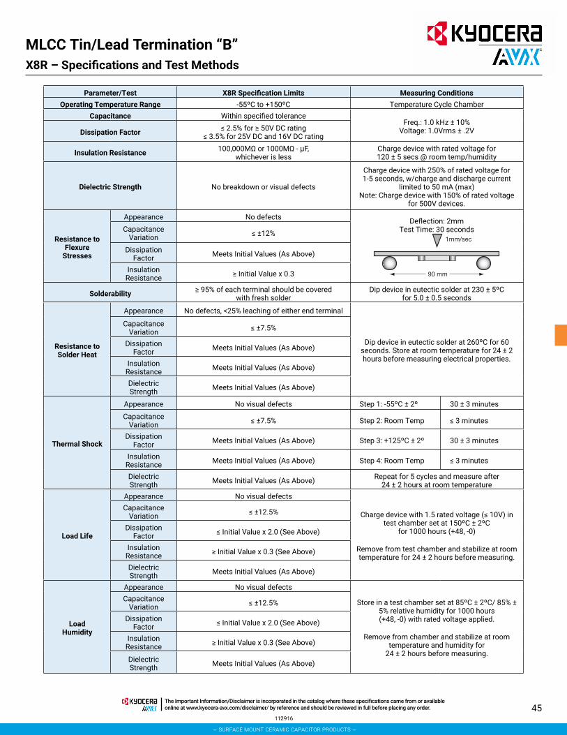
45
MLCC Tin/Lead Termination “B”
112916
Parameter/Test X8R Specification Limits Measuring ConditionsOperating Temperature Range -55ºC to +150ºC Temperature Cycle Chamber
Capacitance Within specified toleranceFreq.: 1.0 kHz ± 10%
Voltage: 1.0Vrms ± .2VDissipation Factor ≤ 2.5% for ≥ 50V DC rating≤ 3.5% for 25V DC and 16V DC rating
Insulation Resistance 100,000MΩ or 1000MΩ - μF,whichever is less
Charge device with rated voltage for120 ± 5 secs @ room temp/humidity
Dielectric Strength No breakdown or visual defects
Charge device with 250% of rated voltage for1-5 seconds, w/charge and discharge current
limited to 50 mA (max)Note: Charge device with 150% of rated voltage
for 500V devices.
Resistance to Flexure
Stresses
Appearance No defects Deflection: 2mmTest Time: 30 seconds
Capacitance Variation ≤ ±12%
Dissipation Factor Meets Initial Values (As Above)
Insulation Resistance ≥ Initial Value x 0.3
Solderability ≥ 95% of each terminal should be coveredwith fresh solder
Dip device in eutectic solder at 230 ± 5ºCfor 5.0 ± 0.5 seconds
Resistance to Solder Heat
Appearance No defects, <25% leaching of either end terminal
Dip device in eutectic solder at 260ºC for 60 seconds. Store at room temperature for 24 ± 2 hours before measuring electrical properties.
Capacitance Variation ≤ ±7.5%
Dissipation Factor Meets Initial Values (As Above)
Insulation Resistance Meets Initial Values (As Above)
Dielectric Strength Meets Initial Values (As Above)
Thermal Shock
Appearance No visual defects Step 1: -55ºC ± 2º 30 ± 3 minutes
Capacitance Variation ≤ ±7.5% Step 2: Room Temp ≤ 3 minutes
Dissipation Factor Meets Initial Values (As Above) Step 3: +125ºC ± 2º 30 ± 3 minutes
Insulation Resistance Meets Initial Values (As Above) Step 4: Room Temp ≤ 3 minutes
Dielectric Strength Meets Initial Values (As Above) Repeat for 5 cycles and measure after
24 ± 2 hours at room temperature
Load Life
Appearance No visual defects
Charge device with 1.5 rated voltage (≤ 10V) in test chamber set at 150ºC ± 2ºC
for 1000 hours (+48, -0)
Remove from test chamber and stabilize at room temperature for 24 ± 2 hours before measuring.
Capacitance Variation ≤ ±12.5%
Dissipation Factor ≤ Initial Value x 2.0 (See Above)
Insulation Resistance ≥ Initial Value x 0.3 (See Above)
Dielectric Strength Meets Initial Values (As Above)
LoadHumidity
Appearance No visual defects
Store in a test chamber set at 85ºC ± 2ºC/ 85% ± 5% relative humidity for 1000 hours (+48, -0) with rated voltage applied.
Remove from chamber and stabilize at room temperature and humidity for
24 ± 2 hours before measuring.
Capacitance Variation ≤ ±12.5%
Dissipation Factor ≤ Initial Value x 2.0 (See Above)
Insulation Resistance ≥ Initial Value x 0.3 (See Above)
DielectricStrength Meets Initial Values (As Above)
Specifications and Test MethodsX8R –
– surface mount ceramic capacitor products –
The Important Information/Disclaimer is incorporated in the catalog where these specifications came from or available online at www.kyocera-avx.com/disclaimer/ by reference and should be reviewed in full before placing any order.

46112916
MLCC Tin/Lead Termination “B”
SIZE LD03 LD05 LD06WVDC 25V 50V 25V 50V 25V 50V
271 Cap 270 G G331 (pF) 330 G G J J471 470 G G J J681 680 G G J J102 1000 G G J J J J152 1500 G G J J J J182 1800 G G J J J J222 2200 G G J J J J272 2700 G G J J J J332 3300 G G J J J J392 3900 G G J J J J472 4700 G G J J J J562 5600 G G J J J J682 6800 G G J J J J822 Cap 8200 G G J J J J103 (μF) 0.01 G G J J J J123 0.012 G G J J J J153 0.015 G G J J J J183 0.018 G G J J J J223 0.022 G G J J J J273 0.027 G G J J J J333 0.033 G G J J J J393 0.039 G G J J J J473 0.047 G G J J J J563 0.056 G N N M M683 0.068 G N N M M823 0.082 N N M M104 0.1 N N M M124 0.12 N N M M154 0.15 N N M M184 0.18 N M M224 0.22 N M M274 0.27 M M334 0.33 M M394 0.39 M474 0.47 M684 0.68824 0.82105 1
WVDC 25V 50V 25V 50V 25V 50VSIZE LD03 LD05 LD06
Letter A C E G J K M N P Q X Y ZMax.
Thickness0.33 0.56 0.71 0.90 0.94 1.02 1.27 1.40 1.52 1.78 2.29 2.54 2.79
(0.013) (0.022) (0.028) (0.035) (0.037) (0.040) (0.050) (0.055) (0.060) (0.070) (0.090) (0.100) (0.110)PAPER EMBOSSED
Capacitance RangeX8R –
– surface mount ceramic capacitor products –
The Important Information/Disclaimer is incorporated in the catalog where these specifications came from or available online at www.kyocera-avx.com/disclaimer/ by reference and should be reviewed in full before placing any order.

47
MLCC Tin/Lead Termination “B”
PART NUMBER (SEE PAGE 4 FOR COMPLETE PART NUMBER EXPLANATION)
LD05 5 C J A 2 AB101
SizeLD03 - 0603LD04 - 0504*LD05 - 0805LD06 - 1206LD10 - 1210LD12 - 1812LD13 - 1825LD14 - 2225LD20 - 2220
DielectricX7R = C
Capacitance Tolerance
B = ±.10 pF (<10pF)C = ±.25 pF (<10pF)D = ±.50 pF (<10pF)F = ±1% (≥ 10 pF)G = ±2% (≥ 10 pF)J = ±5%K = ±10%M = ±20%
Failure Rate
A = Not Applicable
Packaging2 = 7" Reel4 = 13" Reel
Special Code
A = Std. Product
TerminationsB = 5% min leadX = FLEXITERM®
with 5% min lead**
**X7R only
Capacitance Code (In pF)2 Sig. Digits +
Number of Zeros
Voltage6.3V = 610V = Z16V = Y25V = 335V = D50V = 5
100V = 1200V = 2500V = 7
KYOCERA AVX will support those customers for commercial and military Multilayer Ceramic Capacitors with a termination consisting of 5% minimum lead. This termination is indicated by the use of a “B” in the 12th position of the KYOCERA AVX Catalog Part Number. This fulfills KYOCERA AVX’s commitment to providing a full range of products to our customers. KYOCERA AVX has provided in the following pages a full range of values that we are currently offering in this special “B” termination. Please contact the factory if you require additional information on our MLCC Tin/Lead Termination “B” products.
Contact Factory For
Multiples*
*LD04 has the same CV ranges as LD03.
NOTE: Contact factory for availability of Tolerance Options for Specific Part Numbers. Contact factory for non-specified capacitance values.
See FLEXITERM® section for CV options
112916
General SpecificationsX7R –
– surface mount ceramic capacitor products –
The Important Information/Disclaimer is incorporated in the catalog where these specifications came from or available online at www.kyocera-avx.com/disclaimer/ by reference and should be reviewed in full before placing any order.

48
MLCC Tin/Lead Termination “B”
112916
Parameter/Test X7R Specification Limits Measuring ConditionsOperating Temperature Range -55ºC to +125ºC Temperature Cycle Chamber
Capacitance Within specified tolerance
Freq.: 1.0 kHz ± 10% Voltage: 1.0Vrms ± .2VDissipation Factor
≤ 10% for ≥ 50V DC rating≤ 12.5% for 25V DC rating
≤ 12.5% for 25V and 16V DC rating≤ 12.5% for ≤ 10V DC rating
Insulation Resistance 100,000MΩ or 1000MΩ - μF,whichever is less
Charge device with rated voltage for120 ± 5 secs @ room temp/humidity
Dielectric Strength No breakdown or visual defects
Charge device with 250% of rated voltage for1-5 seconds, w/charge and discharge current
limited to 50 mA (max)Note: Charge device with 150% of rated voltage
for 500V devices.
Resistance to Flexure
Stresses
Appearance No defects Deflection: 2mmTest Time: 30 seconds
Capacitance Variation ≤ ±12%
Dissipation Factor Meets Initial Values (As Above)
Insulation Resistance ≥ Initial Value x 0.3
Solderability ≥ 95% of each terminal should be coveredwith fresh solder
Dip device in eutectic solder at 230 ± 5ºCfor 5.0 ± 0.5 seconds
Resistance to Solder Heat
Appearance No defects, <25% leaching of either end terminal
Dip device in eutectic solder at 260ºC for 60 seconds. Store at room temperature for 24 ± 2 hours before measuring electrical properties.
Capacitance Variation ≤ ±7.5%
Dissipation Factor Meets Initial Values (As Above)
Insulation Resistance Meets Initial Values (As Above)
Dielectric Strength Meets Initial Values (As Above)
Thermal Shock
Appearance No visual defects Step 1: -55ºC ± 2º 30 ± 3 minutes
Capacitance Variation ≤ ±7.5% Step 2: Room Temp ≤ 3 minutes
Dissipation Factor Meets Initial Values (As Above) Step 3: +125ºC ± 2º 30 ± 3 minutes
Insulation Resistance Meets Initial Values (As Above) Step 4: Room Temp ≤ 3 minutes
Dielectric Strength Meets Initial Values (As Above) Repeat for 5 cycles and measure after
24 ± 2 hours at room temperature
Load Life
Appearance No visual defects
Charge device with 1.5 rated voltage (≤ 10V) in test chamber set at 125ºC ± 2ºC
for 1000 hours (+48, -0)
Remove from test chamber and stabilize at room temperature for 24 ± 2 hours before measuring.
Capacitance Variation ≤ ±12.5%
Dissipation Factor ≤ Initial Value x 2.0 (See Above)
Insulation Resistance ≥ Initial Value x 0.3 (See Above)
Dielectric Strength Meets Initial Values (As Above)
LoadHumidity
Appearance No visual defects
Store in a test chamber set at 85ºC ± 2ºC/ 85% ± 5% relative humidity for 1000 hours (+48, -0) with rated voltage applied.
Remove from chamber and stabilize at room temperature and humidity for
24 ± 2 hours before measuring.
Capacitance Variation ≤ ±12.5%
Dissipation Factor ≤ Initial Value x 2.0 (See Above)
Insulation Resistance ≥ Initial Value x 0.3 (See Above)
DielectricStrength Meets Initial Values (As Above)
Specifications and Test MethodsX7R –
– surface mount ceramic capacitor products –
The Important Information/Disclaimer is incorporated in the catalog where these specifications came from or available online at www.kyocera-avx.com/disclaimer/ by reference and should be reviewed in full before placing any order.

49
MLCC Tin/Lead Termination “B”
SIZE LD02 LD03 LD05 LD06Soldering Reflow/Wave Reflow/Wave Reflow/Wave Reflow/WavePackaging All Paper All Paper Paper/Embossed Paper/Embossed
(L) Length mm 1.00 ± 0.10 1.60 ± 0.15 2.01 ± 0.20 3.20 ± 0.20(in.) (0.040 ± 0.004) (0.063 ± 0.006) (0.079 ± 0.008) (0.126 ± 0.008)
W) Width mm 0.50 ± 0.10 0.81 ± 0.15 1.25 ± 0.20 1.60 ± 0.20(in.) (0.020 ± 0.004) (0.032 ± 0.006) (0.049 ± 0.008) (0.063 ± 0.008)
(t) Terminal mm 0.25 ± 0.15 0.35 ± 0.15 0.50 ± 0.25 0.50 ± 0.25(in.) (0.010 ± 0.006) (0.014 ± 0.006) (0.020 ± 0.010) (0.020 ± 0.010)
WVDC 16 25 50 6.3 10 16 25 50 100 200 6.3 10 16 25 50 100 200 6.3 10 16 25 50 100 200 500Cap 100(pF) 150
220 C330 C G G G J J J J J J K470 C G G G J J J J J J K680 C G G G J J J J J J K
1000 C G G G J J J J J J K1500 C G G J J J J J J J J J J J J M2200 C G G J J J J J J J J J J J J M3300 C C G G J J J J J J J J J J J J M4700 C C G G J J J J J J J J J J J J M6800 C C G G J J J J J J J J J J J J P
Cap 0.010 C C G G J J J J J J J J J J J J P(μF) 0.015 C G G J J J J J J J J J J J M
0.022 C G G J J J J J N J J J J J M0.033 C G G J J J J N J J J J J M0.047 G G G J J J J N J J J J J M0.068 G G G J J J J N J J J J J P
0.10 C* G G G G J J J J N J J J J P P0.15 G G J J J N N J J J J Q0.22 G G J J N N N J J J J Q0.33 N N N N N J J M P Q0.47 J* N N N N N M M M P Q0.68 N N N M M Q Q Q
1.0 J* J* N N N* M M Q Q Q1.5 P Q Q2.2 J* P* Q Q Q3.34.7 P* P* Q* Q* Q*10 P* P Q* Q* Q22 Q*47
100WVDC 16 25 50 6.3 10 16 25 50 100 200 6.3 10 16 25 50 100 200 6.3 10 16 25 50 100 200 500
SIZE LD02 LD03 LD05 LD06
Letter A C E G J K M N P Q X Y ZMax.
Thickness0.33 0.56 0.71 0.90 0.94 1.02 1.27 1.40 1.52 1.78 2.29 2.54 2.79
(0.013) (0.022) (0.028) (0.035) (0.037) (0.040) (0.050) (0.055) (0.060) (0.070) (0.090) (0.100) (0.110)PAPER EMBOSSED
PREFERRED SIZES ARE SHADED
= Under Development
112916
Capacitance RangeX7R –
– surface mount ceramic capacitor products –
The Important Information/Disclaimer is incorporated in the catalog where these specifications came from or available online at www.kyocera-avx.com/disclaimer/ by reference and should be reviewed in full before placing any order.

50
MLCC Tin/Lead Termination “B”X7R – Capacitance Range
SIZE LD10 LD12 LD13 LD20 LD14Soldering Reflow Only Reflow Only Reflow Only Reflow Only Reflow OnlyPackaging Paper/Embossed All Embossed All Embossed All Embossed All Embossed
(L) Length mm 3.20 + 0.20 4.50 ± 0.30 4.50 ± 0.30 5.70 ± 0.50 5.72 ± 0.25(in.) (0.126 ± 0.008) (0.177 ± 0.012) (0.177 ± 0.012) (0.224 ± 0.020) (0.225 ± 0.010)
W) Width mm 2.50 ± 0.20 3.20 ± 0.20 6.40 ± 0.40 5.00 ± 0.40 6.35 ± 0.25(in.) (0.098 ± 0.008) (0.126 ± 0.008) (0.252 ± 0.016) (0.197 ± 0.016) (0.250 ± 0.010)
(t) Terminal mm 0.50 ± 0.25 0.61 ± 0.36 0.61 ± 0.36 0.64 ± 0.39 0.64 ± 0.39(in.) (0.020 ± 0.010) (0.024 ± 0.014) (0.024 ± 0.014) (0.025 ± 0.015) (0.025 ± 0.015)
WVDC 10 16 25 50 100 200 500 50 100 200 500 50 100 25 50 100 200 50 100Cap 100(pF) 150
220330470680
10001500 J J J J J J M2200 J J J J J J M3300 J J J J J J M4700 J J J J J J M6800 J J J J J J M
Cap 0.010 J J J J J J M K K K K M M X X X M P(μF) 0.015 J J J J J J P K K K P M M X X X M P
0.022 J J J J J J Q K K K P M M X X X M P0.033 J J J J J J Q K K K X M M X X X M P0.047 J J J J J J K K K Z M M X X X M P0.068 J J J J J M K K K Z M M X X X M P
0.10 J J J J J M K K K Z M M X X X M P0.15 J J J J M Z K K P M M X X X M P0.22 J J J J P Z K K P M M X X X M P0.33 J J J J Q K M X M M X X X M P0.47 M M M M Q K P M M X X X M P0.68 M M P X X M Q M P X X M P
1.0 N N P X Z M X M P X X M P1.5 N N Z Z Z Z Z M X X M X2.2 X X Z Z Z Z Z X X M3.3 X X Z Z Z X Z4.7 X X Z Z Z Z X Z10 Z Z Z Z Z Z22 Z Z Z47 Z
100WVDC 10 16 25 50 100 200 500 50 100 200 500 50 100 25 50 100 200 50 100
SIZE LD10 LD12 LD13 LD20 LD14
Letter A C E G J K M N P Q X Y ZMax.
Thickness0.33 0.56 0.71 0.90 0.94 1.02 1.27 1.40 1.52 1.78 2.29 2.54 2.79
(0.013) (0.022) (0.028) (0.035) (0.037) (0.040) (0.050) (0.055) (0.060) (0.070) (0.090) (0.100) (0.110)PAPER EMBOSSED
PREFERRED SIZES ARE SHADED
081021
– surface mount ceramic capacitor products –
The Important Information/Disclaimer is incorporated in the catalog where these specifications came from or available online at www.kyocera-avx.com/disclaimer/ by reference and should be reviewed in full before placing any order.
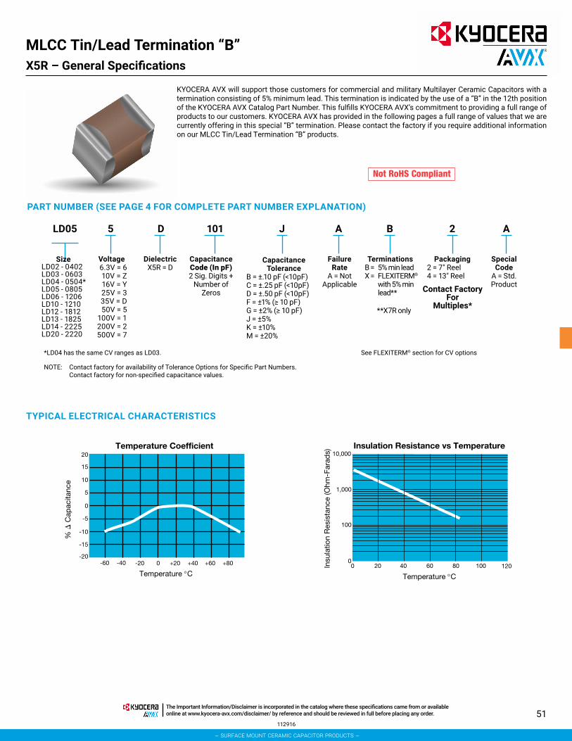
51
MLCC Tin/Lead Termination “B”
PART NUMBER (SEE PAGE 4 FOR COMPLETE PART NUMBER EXPLANATION)
TYPICAL ELECTRICAL CHARACTERISTICS
LD05 5 D J A 2 AB101
DielectricX5R = D
Capacitance Tolerance
B = ±.10 pF (<10pF)C = ±.25 pF (<10pF)D = ±.50 pF (<10pF)F = ±1% (≥ 10 pF)G = ±2% (≥ 10 pF)J = ±5%K = ±10%M = ±20%
Failure Rate
A = Not Applicable
Packaging2 = 7" Reel4 = 13" Reel
Special Code
A = Std. Product
TerminationsB = 5% min leadX = FLEXITERM®
with 5% min lead**
**X7R only
Capacitance Code (In pF)2 Sig. Digits +
Number of Zeros
Voltage6.3V = 610V = Z16V = Y25V = 335V = D50V = 5
100V = 1200V = 2500V = 7
KYOCERA AVX will support those customers for commercial and military Multilayer Ceramic Capacitors with a termination consisting of 5% minimum lead. This termination is indicated by the use of a “B” in the 12th position of the KYOCERA AVX Catalog Part Number. This fulfills KYOCERA AVX’s commitment to providing a full range of products to our customers. KYOCERA AVX has provided in the following pages a full range of values that we are currently offering in this special “B” termination. Please contact the factory if you require additional information on our MLCC Tin/Lead Termination “B” products.
Contact Factory For
Multiples*
*LD04 has the same CV ranges as LD03.
NOTE: Contact factory for availability of Tolerance Options for Specific Part Numbers. Contact factory for non-specified capacitance values.
See FLEXITERM® section for CV options
SizeLD02 - 0402LD03 - 0603LD04 - 0504*LD05 - 0805LD06 - 1206LD10 - 1210LD12 - 1812LD13 - 1825LD14 - 2225LD20 - 2220
%
Cap
acita
nce
-60 -40 -20 0 +20 +40 +60 +80
Temperature °C
Temperature Coefficient20
15
10
5
0
-5
-10
-15
-20
Insu
latio
n R
esis
tanc
e (O
hm-F
arad
s)
1,000
10,000
100
0
Insulation Resistance vs Temperature
0 20 12040 60 80
Temperature °C100
112916
General SpecificationsX5R –
– surface mount ceramic capacitor products –
The Important Information/Disclaimer is incorporated in the catalog where these specifications came from or available online at www.kyocera-avx.com/disclaimer/ by reference and should be reviewed in full before placing any order.

52
MLCC Tin/Lead Termination “B”
Parameter/Test X5R Specification Limits Measuring ConditionsOperating Temperature Range -55ºC to +85ºC Temperature Cycle Chamber
Capacitance Within specified toleranceFreq.: 1.0 kHz ± 10%
Voltage: 1.0Vrms ± .2VFor Cap > 10 μF, 0.5Vrms @ 120HzDissipation Factor
≤ 2.5% for ≥ 50V DC rating≤ 3.0% for 25V, 35V DC rating
≤ 12.5% Max. for 16V DC rating and lower Contact Factory for DF by PN
Insulation Resistance 10,000MΩ or 500MΩ - μF,whichever is less
Charge device with rated voltage for120 ± 5 secs @ room temp/humidity
Dielectric Strength No breakdown or visual defectsCharge device with 250% of rated voltage for1-5 seconds, w/charge and discharge current
limited to 50 mA (max)
Resistance to Flexure
Stresses
Appearance No defects Deflection: 2mmTest Time: 30 seconds
Capacitance Variation ≤ ±12%
Dissipation Factor Meets Initial Values (As Above)
Insulation Resistance ≥ Initial Value x 0.3
Solderability ≥ 95% of each terminal should be coveredwith fresh solder
Dip device in eutectic solder at 230 ± 5ºCfor 5.0 ± 0.5 seconds
Resistance to Solder Heat
Appearance No defects, <25% leaching of either end terminal
Dip device in eutectic solder at 260ºC for 60 seconds. Store at room temperature for 24 ± 2 hours before measuring electrical properties.
Capacitance Variation ≤ ±7.5%
Dissipation Factor Meets Initial Values (As Above)
Insulation Resistance Meets Initial Values (As Above)
Dielectric Strength Meets Initial Values (As Above)
Thermal Shock
Appearance No visual defects Step 1: -55ºC ± 2º 30 ± 3 minutes
Capacitance Variation ≤ ±7.5% Step 2: Room Temp ≤ 3 minutes
Dissipation Factor Meets Initial Values (As Above) Step 3: +85ºC ± 2º 30 ± 3 minutes
Insulation Resistance Meets Initial Values (As Above) Step 4: Room Temp ≤ 3 minutes
Dielectric Strength Meets Initial Values (As Above) Repeat for 5 cycles and measure after
24 ± 2 hours at room temperature
Load Life
Appearance No visual defectsCharge device with 1.5X rated voltage in test
chamber set at 85ºC ± 2ºC for 1000 hours (+48, -0). Note: Contact factory for *optional specification part numbers that are tested at
< 1.5X rated voltage.
Remove from test chamber and stabilize at room temperature for 24 ± 2 hours before measuring.
Capacitance Variation ≤ ±12.5%
Dissipation Factor ≤ Initial Value x 2.0 (See Above)
Insulation Resistance ≥ Initial Value x 0.3 (See Above)
Dielectric Strength Meets Initial Values (As Above)
LoadHumidity
Appearance No visual defects
Store in a test chamber set at 85ºC ± 2ºC/ 85% ± 5% relative humidity for 1000 hours (+48, -0) with rated voltage applied.
Remove from chamber and stabilize at room temperature and humidity for
24 ± 2 hours before measuring.
Capacitance Variation ≤ ±12.5%
Dissipation Factor ≤ Initial Value x 2.0 (See Above)
Insulation Resistance ≥ Initial Value x 0.3 (See Above)
DielectricStrength Meets Initial Values (As Above)
112916
Specifications and Test MethodsX5R –
– surface mount ceramic capacitor products –
The Important Information/Disclaimer is incorporated in the catalog where these specifications came from or available online at www.kyocera-avx.com/disclaimer/ by reference and should be reviewed in full before placing any order.

53
MLCC Tin/Lead Termination “B”
SIZE LD02 LD03 LD05 LD06 LD10 LD12Soldering Reflow/Wave Reflow/Wave Reflow/Wave Reflow/Wave Reflow/WavePackaging All Paper All Paper Paper/Embossed Paper/Embossed Paper/Embossed
(L) Length mm 1.00 ± 0.10 1.60 ± 0.15 2.01 ± 0.20 3.20 ± 0.20 3.20 ± 0.20(in.) (0.040 ± 0.004) (0.063 ± 0.006) (0.079 ± 0.008) (0.126 ± 0.008) (0.126 ± 0.008)
W) Width mm 0.50 ± 0.10 0.81 ± 0.15 1.25 ± 0.20 1.60 ± 0.20 2.50 ± 0.20(in.) (0.020 ± 0.004) (0.032 ± 0.006) (0.049 ± 0.008) (0.063 ± 0.008) (0.098 ± 0.008)
(t) Terminal mm 0.25 ± 0.15 0.35 ± 0.15 0.50 ± 0.25 0.50 ± 0.25 0.50 ± 0.25(in.) (0.010 ± 0.006) (0.014 ± 0.006) (0.020 ± 0.010) (0.020 ± 0.010) (0.020 ± 0.010)
WVDC 4 6.3 10 16 25 50 4 6.3 10 16 25 35 50 6.3 10 16 25 35 50 6.3 10 16 25 35 50 4 6.3 10 16 25 35 50 6.3 10 25 50Cap 100(pF) 150
220 C330 C470 C680 C
1000 C1500 C2200 C3300 C4700 C G6800 C G
Cap 0.010 C G(μF) 0.015 C G G G
0.022 C C G G G N0.033 C G G G N0.047 C C G G G N0.068 C G G N
0.10 C C C G G N N0.15 G N N0.22 C* G G N N Q0.33 G G N0.47 C* C* G N Q Q X0.68 G N
1.0 C* C* C* G G G J* N N P* Q Q X X X1.52.2 C* G* G* J* J* N N N Q Q Z X3.3 J* J* J* J* N N X X4.7 J* J* J* N N N* N* X X X X Q Z10 K* P P P X X X X X Z Z Z22 P* X X X X Z Z Z Z47 X Z*
100 Z* ZWVDC 4 6.3 10 16 25 50 4 6.3 10 16 25 35 50 6.3 10 16 25 35 50 6.3 10 16 25 35 50 4 6.3 10 16 25 35 50 6.3 10 25 50
SIZE LD02 LD03 LD05 LD06 LD10 LD12
Letter A C E G J K M N P Q X Y ZMax.
Thickness0.33 0.56 0.71 0.90 0.94 1.02 1.27 1.40 1.52 1.78 2.29 2.54 2.79
(0.013) (0.022) (0.028) (0.035) (0.037) (0.040) (0.050) (0.055) (0.060) (0.070) (0.090) (0.100) (0.110)PAPER EMBOSSED
PREFERRED SIZES ARE SHADED
*Optional Specifications – Contact factory
NOTE: Contact factory for non-specified capacitance values
112916
Capacitance RangeX5R –
– surface mount ceramic capacitor products –
The Important Information/Disclaimer is incorporated in the catalog where these specifications came from or available online at www.kyocera-avx.com/disclaimer/ by reference and should be reviewed in full before placing any order.

54
Automotive MLCCGeneral Specifications
GENERAL DESCRIPTIONKYOCERA AVX has supported the Automotive Industry requirements for Multilayer Ceramic Capacitors consistently for more than 25 years. Products have been developed and tested specifically for automotive applications and all manufacturing facilities are QS9000 and VDA 6.4 approved.KYOCERA AVX is using AECQ200 as the qualification vehicle for this transition. A detailed qualification package is available on request and contains results on a range of part numbers.
HOW TO ORDER
0805 5 A K 4 2 AT104
DielectricNP0 = AX7R = CX8R = F
Capacitance Tolerance
B = ± 0.1pF (<10pF)*C = ± 0.25pF (<10pF)*D = ± 0.5pF (<10pF)*F = ± 1%*G = ± 2%*J = ± 5% (<=1µF)K = ± 10%M = ± 20%
*NPO only
Failure Rate
4=Automotive
Packaging2 = 7" Reel4 = 13" Reel
Special CodeA = Std.Product
TerminationsT = Plated Ni and SnZ = FLEXITERM®**U = Conductive Epo
**X7R X8R only
Capacitance Code (In pF)2 Sig. Digits +
Number of Zerose.g. 10 F = 106
Voltage6.3V = 610V = Z16V = Y25V = 335V = D50V = 5100V = 1200V = 2500V = 7
Contact factory for availability of Tolerance Options for Specific Part Numbers.
NOTE: Contact factory for non-specified capacitance values 0402 case size available in T termination only.
Size040206030805120612101812
COMMERCIAL VS AUTOMOTIVE MLCC PROCESS COMPARISON
Commercial Automotive
Administrative Standard Part Numbers. No restriction on who purchases these parts.
Specific Automotive Part Number. sed to control supply of product to Automotive customers.
Lot Qualification (Destructive Physical Analysis - DPA) As per EIA RS469 Increased sample plan stricter criteria.
Visual/Cosmetic Quality Standard process and inspection 100% inspection
Application Robustness Standard sampling for accelerated wave solder on X7R dielectrics
Increased sampling for accelerated wave solder on X7R and NP0 followed by lot by lot reliability testing.
All Tests have Accept/Reject Criteria 0/1
062121
– surface mount ceramic capacitor products –
The Important Information/Disclaimer is incorporated in the catalog where these specifications came from or available online at www.kyocera-avx.com/disclaimer/ by reference and should be reviewed in full before placing any order.

55
Automotive MLCCNP0/X7R Dielectric
FLEXITERM FEATURESa) Bend Test
The capacitor is soldered to the PC Board as shown:
a) Temperature Cycle testing FLEXITERM® has the ability to withstand at least 1000 cycles between -55°C and +125°C
Typical bend test results are shown below:
Style Conventional Soft Term0603 >2mm >50805 >2mm >51206 >2mm >5
080818
– surface mount ceramic capacitor products –
The Important Information/Disclaimer is incorporated in the catalog where these specifications came from or available online at www.kyocera-avx.com/disclaimer/ by reference and should be reviewed in full before placing any order.

56
Automotive MLCC-NP0Capacitance Range
SIZE 0402 0603 0805 1206Soldering Reflow/Wave Reflow/Wave Reflow/Wave Reflow/Wave
WVDC 25V 50V 25V 50V 100V 200V 25V 50V 100V 200V 250V 25V 50V 100V 200V 250V 500V0R5 0.5 C C G G G G J J J N N J J J J J J1R0 1.0 C C G G G G J J J N N J J J J J J1R2 1.2 C C G G G G J J J N N J J J J J J1R5 1.5 C C G G G G J J J N N J J J J J J1R8 1.8 C C G G G G J J J N N J J J J J J2R2 2.2 C C G G G G J J J N N J J J J J J2R7 2.7 C C G G G G J J J N N J J J J J J3R3 3.3 C C G G G G J J J N N J J J J J J3R9 3.9 C C G G G G J J J N N J J J J J J4R7 4.7 C C G G G G J J J N N J J J J J J5R6 5.6 C C G G G G J J J N N J J J J J J6R8 6.8 C C G G G G J J J N N J J J J J J8R2 8.2 C C G G G G J J J N N J J J J J J100 10.0 C C G G G G J J J N N J J J J J J120 12 C C G G G G J J J N N J J J J J J150 15 C C G G G G J J J N N J J J J J J180 18 C C G G G G J J J N N J J J J J J220 22 C C G G G G J J J N N J J J J J J270 27 C C G G G G J J J N N J J J J J J330 33 C C G G G G J J J N N J J J J J J390 39 C C G G G G J J J N N J J J J J J470 47 C C G G G G J J J N N J J J J J J510 51 C C G G G G J J J N N J J J J560 56 C C G G G G J J J N N J J J J680 68 C C G G G G J J J N N J J J J820 82 C C G G G G J J J N N J J J J101 100 C C G G G G J J J N N J J J J121 120 G G G J J J N N J J J J151 150 G G G J J J N N J J J J181 180 G G G J J J N N J J J J221 220 G G G J J J N N J J J J271 270 G G G J J J N N J J J J331 330 G G G J J J N N J J J J391 390 G G J J J J J J J471 470 G G J J J J J J J561 560 G G J J J J J J J681 680 G G J J J J J J J821 820 J J J J J J J102 1000 J J J J J J J122 1200152 1500182 1800222 2200272 2700332 3300392 3900472 4700103 10nFWVDC 25V 50V 25V 50V 100V 200V 25V 50V 100V 200V 250V 25V 50V 100V 200V 250V 500VSize 0402 0603 0805 1206
Letter A C E G J K M N P Q X Y Z
Max. Thickness
0.33 0.56 0.71 0.90 0.94 1.02 1.27 1.40 1.52 1.78 2.29 2.54 2.79(0.013) (0.022) (0.028) (0.035) (0.037) (0.040) (0.050) (0.055) (0.060) (0.070) (0.090) (0.100) (0.110)
PAPER EMBOSSED
120920
– surface mount ceramic capacitor products –
The Important Information/Disclaimer is incorporated in the catalog where these specifications came from or available online at www.kyocera-avx.com/disclaimer/ by reference and should be reviewed in full before placing any order.

57
Automotive MLCC - X7RCapacitance Range
Size 0402 0603 0805 1206 1210 1812 2220
Soldering Reflow/Wave Reflow/Wave Reflow/Wave Reflow/Wave Reflow Only Reflow Only Reflow Only
(L) Length
mm(in.)
1 ± 0.1(0.04 ± 0.004)
1.6 ± 0.15(0.063 ± 0.006)
2.01 ± 0.2(0.079 ± 0.008)
3.2 ± 0.2(0.126 ± 0.008)
3.2 ± 0.2(0.126 ± 0.008)
4.5 ± 0.3(0.177 ± 0.012)
5.7 ± 0.5(0.224 ± 0.02)
(W) Width
mm(in.)
0.5 ± 0.1(0.02 ± 0.004)
0.81 ± 0.15(0.032 ± 0.006)
1.25 ± 0.2(0.049 ± 0.008)
1.6 ± 0.2(0.063 ± 0.008)
2.5 ± 0.2(0.098 ± 0.008)
3.2 ± 0.2(0.126 ± 0.008)
5 ± 0.4(0.197 ± 0.016)
(t) Terminal
mm(in.)
0.25 ± 0.15(0.01 ± 0.006)
0.35 ± 0.15(0.014 ± 0.006)
0.5 ± 0.25(0.02 ± 0.01)
0.5 ± 0.25(0.02 ± 0.01)
0.5 ± 0.25(0.02 ± 0.01)
0.61 ± 0.36(0.024 ± 0.014)
0.64 ± 0.39(0.025 ± 0.015)
WVDC 16V 25V 50V 10V 16V 25V 50V 100V 200V 250V 16V 25V 50V 100V 200V 250V 16V 25V 50V 100V 200V 250V 500V 16V 25V 50V 100V 200V 250V 50V 100V 25V 50V 100V 200V 250V 500V
101 100 M Q
221 220 C C C G G G G G G M Q
271 270 C C C G G G G G G M Q
331 330 C C C G G G G G G M Q
391 390 C C C G G G G G G M Q
471 470 C C C G G G G G G M Q
561 560 C C C G G G G G G M Q
681 680 C C C G G G G G G M Q
821 820 C C C G G G G G G M Q
102 1000 C C C G G G G G G G J J J J J J J J J J J J J K K K K M Q K K
122 1220 C C C G G G G G G G J J J J J J J J J J J J J K K K K M Q K K
152 1500 C C C G G G G G G G J J J J J J J J J J J J J K K K K M Q K K
182 1800 C C C G G G G G G G J J J J J J J J J J J J J K K K K M Q K K
222 2200 C C C G G G G G G G J J J J J J J J J J J J J K K K K M Q K K
272 2700 C C C G G G G G G G J J J J J J J J J J J J J K K K K M Q K K
332 3300 C C C G G G G G G G J J J J J J J J J J J J J K K K K M Q K K
392 3900 C C C G G G G G G G J J J J J J J J J J J J J K K K K M Q K K
472 4700 C C C G G G G G G G J J J J J J J J J J J J J K K K K M Q K K
562 5600 C C C G G G G G G G J J J J J J J J J J J J J K K K K M Q K K
682 6800 C C C G G G G G G G J J J J J J J J J J J J J K K K K M Q K K
822 8200 C C C G G G G G G G J J J J J J J J J J J J J K K K K M Q K K
103 Cap 0.01 C C C G G G G G G G J J J J J J J J J J J J J K K K K M Q K K
123 (uF) 0.012 C G G G G G J J J N N N J J J J J J K K K K M Q K K
153 0.015 C G G G G G J J J N N N J J J J J J K K K K M Q K K
183 0.018 C G G G G G J J J N N N J J J J J J K K K K M Q K K
223 0.022 C G G G G G J J J N N N J J J J J J K K K K M Q K K
273 0.027 C G G G G J J J J N N N J J J J J J K K K K M Q K K
333 0.033 C G G G G J J J J N N N J J J J J J K K K K M Q K K
393 0.039 G G G G J J J J N N N J J J J M M K K K K M Q K K
473 0.047 G G G G J J J J N N N J J J M M M K K K K M Q K K
563 0.056 G G G G J J J J N J J J M M M K K K M M Q K K
683 0.068 G G G G J J J J N J J J M M M K K K M M Q K K
823 0.082 G G G G J J J J N J J J M M M K K K M Q Q K K
104 0.1 G G G G J J J J N J J J M P P K K K M Q Q K K X
124 0.12 G J J J J N N J J M M Q Q K K K P Q Q K K
154 0.15 G J J M N N N J J M M Q Q K K K P Q Q K K
224 0.22 G J J M N N N J M M Q Q Q M M M P Q Q M M
334 0.33 N N N N J M P Q P P P Q Z Z X X
474 0.47 N N N N M M P Q P P P Q X X
684 0.68 N N N N M Q Q Q P P Q X X X
105 1 N N N N M Q Q Q P Q Q Z X X Z Z X X
155 1.5 N N Q Q Q Q P Q Z Z X X Z Z Z Z
225 2.2 N N Q Q Q Q Z Z Z Z Z Z Z Z
335 3.3 Q Q Q X Z Z Z Z Z Z
475 4.7 Q Q Q X Z Z Z Z Z Z
106 10 Z Z Z Z Z Z Z
226 22 Z
WVDC 16V 25V 50V 10V 16V 25V 50V 100V 200V 250V 16V 25V 50V 100V 200V 250V 16V 25V 50V 100V 200V 250V 500V 16V 25V 50V 100V 200V 250V 50V 100V 25V 50V 100V 200V 250V 500V
Size 0402 0603 0805 1206 1210 1812 2220
Letter A C E G J K M N P Q X Y ZMax.
Thickness0.33
(0.013)0.56
(0.022)0.71
(0.028)0.90
(0.035)0.94
(0.037)1.02
(0.04)1.27
(0.05)1.40
(0.055)1.52
(0.060)1.78
(0.07)2.29
(0.09)2.54(0.1)
2.79(0.11)
PAPER EMBOSSED
081321
– surface mount ceramic capacitor products –
The Important Information/Disclaimer is incorporated in the catalog where these specifications came from or available online at www.kyocera-avx.com/disclaimer/ by reference and should be reviewed in full before placing any order.

58
Automotive MLCC - X8RCapacitance Range
SIZE 0603 0805 1206Soldering Reflow/Wave Reflow/Wave Reflow/Wave
WVDC WVDC 25V 50V 100V 25V 50V 100V 25V 50V472 pF 4700 G G G J J J J J562 5600 G G G J J J J J682 6800 G G G J J J J J822 8200 G G G J J J J J103 uF 0.01 G G G J J J J J123 0.012 G G J J N J J153 0.015 G G J J N J J183 0.018 G G J J N J J223 0.022 G G J J N J J273 0.027 G G J J J J333 0.033 G G J J J J393 0.039 G G J J J J473 0.047 G G J J J J563 0.056 G N N M M683 0.068 G N N M M823 0.082 N N M M104 0.1 N N M M124 0.12 N N M M154 0.15 N N M M184 0.18 N M M224 0.22 N M M274 0.27 M M334 0.33 M M394 0.39 M M474 0.47 M Q684 0.68 Q Q824 0.82 Q Q105 1 Q Q
WVDC WVDC 25V 50V 100V 25V 50V 100V 25V 50VSIZE 0603 0805 1206
Letter A C E G J K M N P Q X Y ZMax.
Thickness0.33
(0.013)0.56
(0.022)0.71
(0.028)0.90
(0.035)0.94
(0.037)1.02
(0.040)1.27
(0.050)1.40
(0.055)1.52
(0.060)1.78
(0.070)2.29
(0.090)2.54
(0.100)2.79
(0.110)PAPER EMBOSSED
080221
– surface mount ceramic capacitor products –
The Important Information/Disclaimer is incorporated in the catalog where these specifications came from or available online at www.kyocera-avx.com/disclaimer/ by reference and should be reviewed in full before placing any order.

59
Surface Mount NP0, X7R and X8R/L MLCCs
KYOCERA AVX's APS COTS+ series of multilayer ceramic capacitors offers the customer a high reliability solution with an ultralow failure rate, <1ppb, in a variety of case sizes and voltages. The APS range encompasses a wide range of dielectric types to meet the customer's requirements from low temperature/voltage capacitance change dielectric, NP0, to high preforming capacitance voltage X7R to high temperature reliability dielectrics, X8R/L.APS capacitors have a wider capacitance range than MIL spec parts that satisfies the need for higher CV demands and board space saving requirements. Each production lot is extensively tested and removes the requirement for customer specific drawings. The testing regime uses many of the MIL-STD test methods as per MIL-PRF-55681 and has a field failure rate of less than 1 ppb. The APS testing series uses KYOCERA AVX’s unique in-house maverick testing detection system that eliminates infant mortality failures.Applications suitable for APS include Industrial, Telecommunications, Aviation, and Military. The APS is available with a range of different termination finishes, Flexiterm®, Nickel / Tin and Tin with Pb1. Flexiterm® technology delivers improved thermo-mechanical stress resistance.
Dielectric Temperature/Percentage Cap Change
NP0 -30ppm +30ppm from -55°C + 125°C
X7R -15% +15% from -55°C to + 125°C
X8R -15% +15% from -55°C to + 150°C
X8L -15% +40% from -55°C to + 150°C
FEATURES• The APS range has been extensively
reliability tested as standard resulting in an ultralow failure rate, ≤1ppb
• The APS range is available with Flexiterm® that deliver’s high thermo-mechanical stress resistance.
• High CV range enabling board space saving requirements.
HOW TO ORDER
5
Voltage10V = Z16V = Y25V = 350V = 5100V = 1200V = 2250V = V500V = 7
A
Dielectric
NP0 = AX7R = CX8R = FX8L = L
K
Capacitance Tolerance
J = ±5%K = ±10%M = ±20%
Q
Failure Rate
Q = APS
2
Packaging2 = 7" Reel4 = 13" Reel
A
Special CodeA = Std.Product
T
TerminationsT = Plated Ni and SnZ = FLEXITERM®**B = 10% min leadX = FLEXITERM® with
10% min lead
Z,X for X7R only**RoHS compliant
104
Capacitance Code (In pF)
2 Sig. Digits +Number of Zeros
e.g. 10 F = 106
NOTE: Contact factory for availability of Termination and Tolerance Options for Specific Part Number.
AP03
SizeAP03=0603AP05=0805AP06=1206AP10=1210AP12=1812AP20=2220
General Specifications
010920
APS for COTS+ High Reliability Applications
APS RELIABILITY TEST SUMMARY• 100% Visual Inspection• DPA• IR, DF, Cap, DWV• Maverick Lot Review• Thermal Shocl• 85/85 Testing• Additional Life Testing• C of C with every Order• Quarterly Data Package
– surface mount ceramic capacitor products –
The Important Information/Disclaimer is incorporated in the catalog where these specifications came from or available online at www.kyocera-avx.com/disclaimer/ by reference and should be reviewed in full before placing any order.

60
Size AP03 = 0603 AP05 = 0805 AP06 = 1206 AP10 = 1210WVDC 25V 50V 100V 25V 50V 100V 25V 50V 100V 200V 500V 25V 50V 100V 200V
100 10pF G G G J J J J J J J J120 12 G G G J J J J J J J J150 15 G G G J J J J J J J J180 18 G G G J J J J J J J220 22 G G G J J J J J J J270 27 G G G J J J J J J J330 33 G G G J J J J J J J390 39 G G G J J J J J J J470 47 G G G J J J J J J J510 51 G G G J J J J J J J560 56 G G G J J J J J J J680 68 G G G J J J J J J J820 82 G G G J J J J J J J101 100 G G G J J J J J J J121 120 G G G J J J J J J J151 150 G G G J J J J J J J181 180 G G G J J J J J J J221 220 G G G J J J J J J J271 270 G G G J J J J J J J331 330 G G G J J J J J J J391 390 G G J J J J J J J471 470 G G J J J J J J J561 560 J J J J J J J681 680 J J J J J J J821 820 J J J J J J J102 1000 J J J J J J J J J J J122 1200 J J M M152 1500 J J M M182 1800 J J M M222 2200 J J M M272 2700332 3300392 3900472 4700103 10nF
WVDC 25V 50V 100V 25V 50V 100V 25V 50V 100V 200V 500V 25V 50V 100V 200VSize AP03 = 0603 AP05 = 0805 AP06 = 1206 AP10 = 1210
Letter A C E G J K M N P Q X Y Z
Max. Thickness
0.33 0.56 0.71 0.90 0.94 1.02 1.27 1.40 1.52 1.78 2.29 2.54 2.79(0.013) (0.022) (0.028) (0.035) (0.037) (0.040) (0.050) (0.055) (0.060) (0.070) (0.090) (0.100) (0.110)
PAPER EMBOSSED
APS COTS+ NP0 SeriesCapacitance Range
TS 16949, ISO 9001Certified
082917
– surface mount ceramic capacitor products –
The Important Information/Disclaimer is incorporated in the catalog where these specifications came from or available online at www.kyocera-avx.com/disclaimer/ by reference and should be reviewed in full before placing any order.

61
Letter A C E G J K M N P Q X Y ZMax.
Thickness0.33 0.56 0.71 0.90 0.94 1.02 1.27 1.40 1.52 1.78 2.29 2.54 2.79
(0.013) (0.022) (0.028) (0.035) (0.037) (0.040) (0.050) (0.055) (0.060) (0.070) (0.090) (0.100) (0.110)PAPER EMBOSSED
APS COTS+ X7R SeriesCapacitance Range
TS 16949, ISO 9001Certified
Size AP03 = 0603 AP05 = 0805 AP06 = 1206 AP10 = 1210 AP12 = 1812 AP20 = 2220WVDC 16V 25V 50V 100V 200V 16V 25V 50V 100V 200V 16V 25V 50V 100V 200V 500V 16V 25V 50V 100V 50V 100V 25V 50V 100V
102 Cap 1000 G G G G G J J J J J J J J J J J K K K K K K182 (pF) 1800 G G G G J J J J J J J J J J J K K K K K K222 2200 G G G G J J J J J J J J J J J K K K K K K332 3300 G G G G J J J J J J J J J J J K K K K K K472 4700 G G G G J J J J J J J J J J J K K K K K K103 0.01 G G G G J J J J J J J J J J J K K K K K K123 0.012 G G G J J J M J J J J J K K K K K K153 0.015 G G G J J J M J J J J J K K K K K K183 0.018 G G G J J J M J J J J J K K K K K K223 0.022 G G G J J J M J J J J J K K K K K K273 0.027 G G G J J J M J J J J J K K K K K K333 0.033 G G G J J J M J J J J J K K K K K K473 0.047 G G G J J J M J J J M J K K K K K K563 0.056 G G G J J J M J J J M J K K K M K K683 0.068 G G G J J J M J J J M J K K K M K K823 0.082 G G G J J J M J J J M J K K K M K K104 0.1 G G G J J M M J J J M J K K K M K K124 0.12 J J M N J J M M K K K P K K154 0.15 M N M N J J M M K K K P K K224 0.22 M N M N J M M Q M M M P M M334 0.33 N N M N J M P Q P P P Q X X474 0.47 N N M N M M P Q P P P Q X X684 0.68 N N N M Q Q Q P P Q X X X105 Cap 1.0 N N N* M Q Q Q* P Q Q Z* X X155 (μF) 1.5 Q Q Q P Q Z Z X X225 2.2 Q Q Q Z Z Z Z* Z Z335 3.3 Q X Z Z Z Z475 4.7 Q X Z Z Z*106 10 Z Z* Z Z*226 22 Z
WVDC 16V 25V 50V 100V 200V 16V 25V 50V 100V 200V 16V 25V 50V 100V 200V 500V 16V 25V 50V 100V 50V 100V 25V 50V 100VSize AP03 = 0603 AP05 = 0805 AP06 = 1206 AP10 = 1210 AP12 = 1812 AP20 = 2220
*Not currently available with lead plating finish, contact plant for further information.
102620
– surface mount ceramic capacitor products –
The Important Information/Disclaimer is incorporated in the catalog where these specifications came from or available online at www.kyocera-avx.com/disclaimer/ by reference and should be reviewed in full before placing any order.

62
SIZE AP03 = 0603 AP05 = 0805 AP06 = 1206WVDC 25V 50V 25V 50V 25V 50V
331 Cap 330 G G J J471 (pF) 470 G G J J681 680 G G J J102 1000 G G J J J J152 1500 G G J J J J222 2200 G G J J J J332 3300 G G J J J J472 4700 G G J J J J682 6800 G G J J J J103 Cap 0.01 G G J J J J153 (μF) 0.015 G G J J J J223 0.022 G G J J J J333 0.033 G G J J J J473 0.047 G G J J J J683 0.068 G N N M M104 0.1 N N M M154 0.15 N N M M224 0.22 N M M334 0.33 M M474 0.47 M684 0.68105 1
WVDC 25V 50V 25V 50V 25V 50VSIZE 0603 0805 1206
SIZE AP03 = 0603 AP05 = 0805 AP06 = 1206WVDC 25V 50V 100V 25V 50V 100V 16V 25V 50V 100V
331 Cap 330 G G J J471 (pF) 470 G G J J681 680 G G J J102 1000 G G J J152 1500 G G J J J J222 2200 G G J J J J332 3300 G G J J J J472 4700 G G J J J J682 6800 G G J J J J103 Cap 0.01 G G J J J J153 (μF) 0.015 G G J J J J J223 0.022 G G J J J J J333 0.033 G G J J N J J473 0.047 G G J J N J J683 0.068 G G J J J J104 0.1 G G J J J M154 0.15 J N J J J Q224 0.22 N N J J J Q334 0.33 N J M P Q474 0.47 N M M P684 0.68 M105 1 M
WVDC 25V 50V 100V 25V 50V 100V 16V 25V 50V 100VSIZE 0603 0805 1206
Letter A C E G J K M N P Q X Y Z
Max. Thickness
0.33 0.56 0.71 0.90 0.94 1.02 1.27 1.40 1.52 1.78 2.29 2.54 2.79(0.013) (0.022) (0.028) (0.035) (0.037) (0.040) (0.050) (0.055) (0.060) (0.070) (0.090) (0.100) (0.110)
PAPER EMBOSSED
APS COTS+ X8R/L SeriesCapacitance Range
TS 16949, ISO 9001Certified
X8R
X8L
082917
– surface mount ceramic capacitor products –
The Important Information/Disclaimer is incorporated in the catalog where these specifications came from or available online at www.kyocera-avx.com/disclaimer/ by reference and should be reviewed in full before placing any order.

63
General Specifications
GENERAL DESCRIPTIONWith increased requirements from the automotive industry for additional component robustness, KYOCERA AVX recognized the need to produce a MLCC with enhanced mechanical strength. It was noted that many components may be subject to severe flexing and vibration when used in various under the hood automotive and other harsh environment applications.To satisfy the requirement for enhanced mechanical strength, KYOCERA AVX had to find a way of ensuring electrical integrity is maintained whilst external forces are being applied to the component. It was found that the structure of the termination needed to be flexible and after much research and development, KYOCERA AVX launched FLEXITERM®. FLEXITERM® is designed to enhance the mechanical flexure and temperature cycling performance of a standard ceramic capacitor with an X7R dielectric. The industry standard for flexure is 2mm minimum. Using FLEXITERM®, KYOCERA AVX provides up to 5mm of flexure without internal cracks. Beyond 5mm, the capacitor will generally fail “open”.As well as for automotive applications FLEXITERM® will provide Design Engineers with a satisfactory solution when designing PCB’s which may be subject to high levels of board flexure.
APPLICATIONS
High Flexure Stress Circuit Boards• e.g. Depanelization: Components near edges of board.Variable Temperature Applications• Soft termination offers improved reliability performance in
applications where there is temperature variation.• e.g. All kind of engine sensors: Direct connection to battery rail.Automotive Applications• Improved reliability.• Excellent mechanical performance and thermo mechanical
performance.
HOW TO ORDER
0805 5 C K A 2 AZ104
DielectricC = X7RF = X8R
Capacitance ToleranceJ = ±5%*K = ±10%M = ±20%
*≤1μF only
Failure Rate
A=Commercial4 = Automotive
Packaging2 = 7" Reel4 = 13" Reel
Special CodeA = Std.Product
TerminationsZ = FLEXITERM®
For FLEXITERM® with Tin/Lead
termination see LD Series
Capacitance Code (In pF)2 Sig Digits +
Number of Zerose.g., 104 = 100nF
Voltage6 = 6.3VZ = 10VY = 16V3 = 25V5 = 50V1 = 100V2 = 200V
NOTE: Contact factory for availability of Tolerance Options for Specific Part Numbers.
Style060308051206121018122220
091120
MLCC with FLEXITERM®
PRODUCT ADVANTAGES• High mechanical performance able to withstand,
5mm bend test guaranteed• Increased temperature cycling performance, 3000
cycles and beyond• Flexible termination system• Reduction in circuit board flex failures• Base metal electrode system• Automotive or commercial grade products available• AECQ200 Qualified• Approved to VW 80808 Specification
– surface mount ceramic capacitor products –
The Important Information/Disclaimer is incorporated in the catalog where these specifications came from or available online at www.kyocera-avx.com/disclaimer/ by reference and should be reviewed in full before placing any order.

64
MLCC with FLEXITERM®
Specifications and Test Methods
PERFORMANCE TESTING
AEC-Q200 Qualification:• Created by the Automotive Electronics
Council• Specification defining stress
test qualification for passive components
Testing:Key tests used to compare soft termination to AEC-Q200 qualification:• Bend Test• Temperature Cycle Test
BOARD BEND TEST PROCEDUREAccording to AEC-Q200
BOARD BEND TEST RESULTSAEC-Q200 Vrs FLEXITERM® Bend Test
Test Procedure as per AEC-Q200:Sample size: 20 componentsSpan: 90mm Minimum deflection spec: 2 mm
• Components soldered onto FR4 PCB (Figure 1)• Board connected electrically to the test equipment
(Figure 2)
BEND TESTPLATE
CONTROL PANEL
CONNECTOR
Fig 1 - PCB layout with electrical connections
DIGITALCALIPER
MOUNTINGASSEMBLY
LOADINGKNIFE
CONTROLPANEL
Fig 2 - Board Bend test equipment
120603
1086420
NPO X7R X7R soft term
121206
Sub
stra
te B
end
(mm
)S
ubst
rate
Ben
d (m
m)
Sub
stra
te B
end
(mm
)S
ubst
rate
Ben
d (m
m)
1086420
NPO X7R X7R soft term
120805
1086420
NPO X7R X7R soft term
121210
1086420
NPO X7R X7R soft term Max. = 10mm
90mm
Max. = 10mm
Test Temperature Profile (1 cycle)
TABLE SUMMARYTypical bend test results are shown below:Style Conventional Termination FLEXITERM® 0603 >2mm >5mm0805 >2mm >5mm1206 >2mm >5mm
TEMPERATURE CYCLE TEST PROCEDURETest Procedure as per AEC-Q200:The test is conducted to determine the resistance of the component when it is exposed to extremes of alternating high and low temperatures.• Sample lot size quantity 77 pieces• TC chamber cycle from -55ºC to +125ºC for 1000 cycles• Interim electrical measurements at 250, 500, 1000 cycles• Measure parameter capacitance dissipation factor, insulation
resistance
ENHANCED SOFT TERMINATION BEND TEST PROCEDURE
Bend TestThe capacitor is soldered to the printed circuit board as shown and is bent up to 10mm at 1mm per second:
• The board is placed on 2 supports 90mm apart (capacitor side down)
• The row of capacitors is aligned with the load stressing knife
• The load is applied and the deflection where the part starts to crack is recorded (Note: Equipment detects the start of the crack using a highly sensitive current detection circuit)
• The maximum deflection capability is 10mm
020117
– surface mount ceramic capacitor products –
The Important Information/Disclaimer is incorporated in the catalog where these specifications came from or available online at www.kyocera-avx.com/disclaimer/ by reference and should be reviewed in full before placing any order.

65
MLCC with FLEXITERM®
Specifications and Test Methods
BEYOND 1000 CYCLES: TEMPERATURE CYCLE TEST RESULTS
% F
ailu
re
10
8
6
4
2
00 500 1000 1500
0603
2000 2500 3000
% F
ailu
re
10
8
6
4
2
00 500 1000 1500
1206
2000 2500 3000
% F
ailu
re
10
8
6
4
2
00 500 1000 1500
0805
2000 2500 3000
% F
ailu
re
10
8
6
4
2
00 500 1000 1500
1210
2000 2500 3000
Soft Term - No Defects up to 3000 cyclesAEC-Q200 specification states 1000 cycles compared to 3000 temperature cycles.
FLEXITERM® TEST SUMMARY
• Qualified to AEC-Q200 test/specification with the exception of using 3000 temperature cycles (up to +150°C bend test guaranteed greater than 5mm).
• FLEXITERM® provides improved performance compared to standard termination systems.
• Board bend test improvement by a factor of 2 to 4 times.• Temperature Cycling:
– 0% Failure up to 3000 cycles – No ESR change up to 3000 cycle
WITHOUT SOFT TERMINATION WITH SOFT TERMINATION
Major fear is of latent board flex failures.Far superior mechanical performance.
Generally open failure mode beyond5mm flexure
061120
Green = Soft Term MLCC (Flexiterm)Red = Standard MLCC
– surface mount ceramic capacitor products –
The Important Information/Disclaimer is incorporated in the catalog where these specifications came from or available online at www.kyocera-avx.com/disclaimer/ by reference and should be reviewed in full before placing any order.

66
MLCC with FLEXITERM®
X8R Dielectric
SIZE 0603 0805 1206Soldering Reflow/Wave Reflow/Wave Reflow/Wave
WVDC 25V 50V 25V 50V 25V 50V271 Cap 270 G G331 (pF) 330 G G J J471 470 G G J J681 680 G G J J102 1000 G G J J J J152 1500 G G J J J J182 1800 G G J J J J222 2200 G G J J J J272 2700 G G J J J J332 3300 G G J J J J392 3900 G G J J J J472 4700 G G J J J J562 5600 G G J J J J682 6800 G G J J J J822 8200 G G J J J J103 Cap 0.01 G G J J J J123 (μF) 0.012 G G J J J J153 0.015 G G J J J J183 0.018 G G J J J J223 0.022 G G J J J J273 0.027 G G J J J J333 0.033 G G J J J J393 0.039 G G J J J J473 0.047 G G J J J J563 0.056 G N N M M683 0.068 G N N M M823 0.082 N N M M104 0.1 N N M M124 0.12 N N M M154 0.15 N N M M184 0.18 N M M224 0.22 N M M274 0.27 M M334 0.33 M M394 0.39 M474 0.47 M684 0.68824 0.82105 1
WVDC 25V 50V 25V 50V 25V 50VSIZE 0603 0805 1206
Letter A C E G J K M N P Q X Y ZMax.
Thickness0.33
(0.013)0.56
(0.022)0.71
(0.028)0.90
(0.035)0.94
(0.037)1.02
(0.040)1.27
(0.050)1.40
(0.055)1.52
(0.060)1.78
(0.070)2.29
(0.090)2.54
(0.100)2.79
(0.110)PAPER EMBOSSED
TS 16949, ISO 9001Certified
Capacitance Range
020117
– surface mount ceramic capacitor products –
The Important Information/Disclaimer is incorporated in the catalog where these specifications came from or available online at www.kyocera-avx.com/disclaimer/ by reference and should be reviewed in full before placing any order.

67
Letter A C E G J K M N P Q X Y ZMax.
Thickness0.33
(0.013)0.56
(0.022)0.71
(0.028)0.90
(0.035)0.94
(0.037)1.02
(0.040)1.27
(0.050)1.40
(0.055)1.52
(0.060)1.78
(0.070)2.29
(0.090)2.54
(0.100)2.79
(0.110)PAPER EMBOSSED
Size 0402 0603 0805 1206 1210 1812 2220Soldering Reflow/ Wave Reflow/Wave Reflow/Wave Reflow/Wave Reflow Only Reflow Only Reflow Only
WVDC 16V 25V 50V 10V 16V 25V 50V 100 V 200V 250V 16V 25V 50V 100 V 200V 250V 16V 25V 50V 100 V 200V 250V 500V 16V 25V 50V 100V 50V 100 V 25V 50V 100 V221 Cap 220 C C C C271 (pF) 270 C C C331 330 C C C391 390 C C C471 470 C C C561 560 C C C681 680 C C C821 820 C C C102 1000 C C C G G G G G G J J J J J J J J J J J J J K K K K N N182 1800 C C C G G G G G G J J J J J J J J J J J J J K K K K N N222 2200 C C C G G G G G G J J J J J J J J J J J J J K K K K N N332 3300 C C C G G G G G G J J J J J J J J J J J J J K K K K N N472 4700 C C C G G G G G G J J J J J J J J J J J J J K K K K N N103 Cap 0.01 C G G G G G G J J J J J J J J J J J J J K K K K N N123 (μF) 0.012 C G G G J J J N N N J J J J J J K K K K N N153 0.015 C G G G J J J N N N J J J J J J K K K K N N183 0.018 C G G G J J J N N N J J J J J J K K K K N N223 0.022 C G G G J J J N N N J J J J J J K K K K N N273 0.027 C G G G J J J N N N J J J J J J K K K K N N333 0.033 C G G G J J J N N N J J J J J J K K K K N N473 0.047 G G G J J J N N N J J J M J J K K K K N N563 0.056 G G G J J J N J J J M J J K K K M N N683 0.068 G G G J J J N J J J M J J K K K M N N823 0.082 G G G J J J N J J J M J J K K K M N N104 0.1 C G G G J J J N J J J M J J K K K M N N124 0.12 J J N N J J M M K K K P N N154 0.15 M N N N J J M M K K K P N N224 0.22 G J J J M N N N J M M Q M M M P N N334 0.33 N N N N J M P Q P P P Q X X474 0.47 J J J N N N N M M P Q P P P Q X X684 0.68 N N N N M Q Q Q P P Q X X X105 1 N N N N M Q Q Q P Q Q Z X X155 1.5 N N Q Q Q P Q Z Z X X225 2.2 N N Q Q Q X Z Z Z Z Z335 3.3 Q Q X Z Z Z Z475 4.7 Q Q X Z Z Z Z Z106 10 Z Z Z Z Z226 22 Z
WVDC 16V 25V 50V 10V 16V 25V 50V 100 V 200V 250V 16V 25V 50V 100 V 200V 250V 16V 25V 50V 100 V 200V 250V 500V 16V 25V 50V 100 V 50V 100 V 25V 50V 100 VSize 0402 0603 0805 1206 1210 1812 2220
MLCC with FLEXITERM®
X7R DielectricCapacitance Range
111020
– surface mount ceramic capacitor products –
The Important Information/Disclaimer is incorporated in the catalog where these specifications came from or available online at www.kyocera-avx.com/disclaimer/ by reference and should be reviewed in full before placing any order.

68
FLEXISAFE MLC ChipsGeneral Specifications and Capacitance RangeFor Ultra Safety Critical Applications
012721
KYOCERA AVX have developed a range of components specifically for safety critical applications.Utilizing the award-winning FLEXITERM™ layer in conjunction with the cascade design previously used for high voltage MLCCs, a range of ceramic capacitors is now available for customers who require components designed with an industry leading set of safety features.The FLEXITERM™ layer protects the component from any damage to the ceramic resulting from mechanical stress during PCB assembly or use with end customers. Board flexure type mechanical damage accounts for the majority of MLCC failures. The addition of the cascade structure protects the component from low insulation resistance failure resulting from other common causes for failure; thermal stress damage, repetitive strike ESD damage and placement damage. With the inclusion of the cascade design structure to complement the FLEXITERM™ layer, the FLEXISAFE range of capacitors has unbeatable safety features. Flexisafe capacitors are qualified in accordance with AEC-Q200 standard. AEC-Q200 detailed qualification data is available on request
HOW TO ORDER
FS05 5 C K Q 2 AZ104
DielectricX7R = C
Capacitance Tolerance
J = ±5%K = ±10%M = ±20%
Failure Rate
A = Commercial4 = Automotive
Q = APS
Packaging2 = 7" Reel
4 = 13" Reel
Special Code
A = Std.Product
TerminationsZ = FLEXITERM™*X = FLEXITERM™ with 5% min lead
*Not RoHS Compliant
Capacitance Code (In pF)2 Sig. Digits +
Number of Zeros
e.g. 10μF =106
Voltage16V = Y25V = 350V = 5
100V = 1
SizeFS03 = 0603FS05 = 0805FS06 = 1206FS10 = 1210
CAPACITANCE RANGE FLEXISAFE X7R
SIZE FS03 = 0603 FS05 = 0805 FS06 = 1206 FS10 = 1210WVDC 16 25 50 100 16 25 50 100 16 25 50 16 25 50
102 1000 G G G G J J J J J J J182 1800 G G G G J J J J J J J222 2200 G G G G J J J J J J J332 3300 G G G G J J J J J J J472 4700 G G G G J J J J J J J682 6800 G G G G J J J J J J J103 0.01 G G G G J J J J J J J123 0.012 G G G J J J J J J J153 0.015 G G G J J J J J J J183 0.018 G G G J J J J J J J223 0.022 G G G N N N N J J J273 0.027 N N N N J J J333 0.033 N N N N J J J473 0.047 N N N N M M M563 0.056 N N N N M M M683 0.068 N N N N M M M823 0.082 N N N N M M M104 0.1 N N N N M M M124 0.12 M M M154 0.15 M M M Q Q Q224 0.22 Q Q Q334 0.33 Q Q Q474 0.47 Q Q Q
Letter G J M N QMax. Thickness 0.90 (0.035) 0.94 (0.037) 1.27 (0.050) 1.40 (0.055) 1.78 (0.070)
PAPER EMBOSSED
– surface mount ceramic capacitor products –
The Important Information/Disclaimer is incorporated in the catalog where these specifications came from or available online at www.kyocera-avx.com/disclaimer/ by reference and should be reviewed in full before placing any order.

69
Capacitor Array (IPC)
032417
BENEFITS OF USING CAPACITOR ARRAYS
KYOCERA AVX capacitor arrays offer designers the opportunity to lower placement costs, increase assembly line output through lower component count per board and to reduce real estate requirements.
Reduced CostsPlacement costs are greatly reduced by effectively placing one device instead of four or two. This results in increased throughput and translates into savings on machine time. Inventory levels are lowered and further savings are made on solder materials, etc.
Space SavingSpace savings can be quite dramatic when compared to the use of discrete chip capacitors. As an example, the 0508 4-element array offers a space reduction of >40% vs. 4 x 0402 discrete capacitors and of >70% vs. 4 x 0603 discrete capacitors. (This calculation is dependent on the spacing of the discrete components.)
Increased ThroughputAssuming that there are 220 passive components placed in a mobile phone:A reduction in the passive count to 200 (by replacing discrete components with arrays) results in an increase in throughput of approximately 9%.A reduction of 40 placements increases throughput by 18%.
For high volume users of cap arrays using the very latest placement equipment capable of placing 10 components per second, the increase in throughput can be very significant and can have the overall effect of reducing the number of placement machines required to mount components:If 120 million 2-element arrays or 40 million 4-element arrays were placed in a year, the requirement for placement equipment would be reduced by one machine.During a 20Hr operational day a machine places 720K components. Over a working year of 167 days the machine can place approximately 120 million. If 2-element arrays are mounted instead of discrete components, then the number of placements is reduced by a factor of two and in the scenario where 120 million 2-element arrays are placed there is a saving of one pick and place machine.Smaller volume users can also benefit from replacing discrete components with arrays. The total number of placements is reduced thus creating spare capacity on placement machines. This in turn generates the opportunity to increase overall production output without further investment in new equipment.
W2A (0508) Capacitor Arrays
W3A (0612) Capacitor Arrays
The 0508 4-element capacitor array gives a PCB space saving of over 40% vs four 0402 discretes and over 70% vs four 0603 discrete capacitors.
The 0612 4-element capacitor array gives a PCB space saving of over 50% vs four 0603 discretes and over 70% vs four 0805 discrete capacitors.
AREA = 7.0mm2 (0.276 in2) AREA = 3.95mm2 (0.156 in2)5.0 (0.197)
1.4(0.055)
1.0(0.039)
2.1 (0.083)
1.88(0.074)
4 pcs 0402 Capacitors = 1 pc 0508 Array
AREA = 13.8mm2 (0.543 in2) AREA = 6.4mm2 (0.252 in2)6.0 (0.236)
2.3(0.091)
1.5(0.059)
3.2 (0.126)
1.60(0.063)
4 pcs 0603 Capacitors = 1 pc 0612 Array
Capacitor Array
– surface mount ceramic capacitor products –
The Important Information/Disclaimer is incorporated in the catalog where these specifications came from or available online at www.kyocera-avx.com/disclaimer/ by reference and should be reviewed in full before placing any order.

70
Capacitor ArrayCapacitor Array (IPC)
0508 - 2 Element
0508 - 4 Element 0612 - 4 Element
GENERAL DESCRIPTIONKYOCERA AVX is the market leader in the development and manufacture of capacitor arrays. The array family of products also includes the 0612 4-element device as well as 0508 2-element and 4-element series, all of which have received widespread acceptance in the marketplace.KYOCERA AVX capacitor arrays are available in X5R, X7R and NP0 (C0G) ceramic dielectrics to cover a broad range of capacitance values. Voltage ratings from 6.3 Volts up to 100 Volts are offered. KYOCERA AVX also now offers a range of automotive capacitor arrays qualified to AEC-Q200 (see separate table).Key markets for capacitor arrays are Mobile and Cordless Phones, Digital Set Top Boxes, Computer Motherboards and Peripherals as well as Automotive applications, RF Modems, Networking Products, etc.
AVX Capacitor Array - W2A41A***KS21 Magnitude
-40
-35
-30
-25
-20
-15
-10
-5
0
0111.010.0
Frequency (GHz)
S21
mag
. (d
B)
5pF 10pF
15pF 22pF
33pF 39pF
68pF
HOW TO ORDER
W 2 A C34 M A 2AT103
Array DielectricA = NP0C = X7RD = X5R
Voltage6 = 6VZ = 10VY = 16V3 = 25V5 = 50V1 = 100V
Number of Caps
2 = 2 Element4 = 4 Element
Capacitance Tolerance
J = ±5%K = ±10%M = ±20%
Failure Rate
A = Commercial4 = Automotive
Packaging & Quantity
Code2A = 7" Reel
(4000)4A = 13" Reel
(10000)2F = 7" Reel
(1000)
Termination Code
*T = Plated Ni and Sn
*Z = FLEXITERM®
*B = 5% min lead*X = FLEXITERM®
with 5% min lead
Capacitance Code
2 Sig. Digits + Number of
Zeros
Case Size
2 = 05083 = 0612
StyleW = RoHSL = SnPb
NOTE: Contact factory for availability of Termination and Tolerance Options for Specific Part Numbers.
032417
– surface mount ceramic capacitor products –
The Important Information/Disclaimer is incorporated in the catalog where these specifications came from or available online at www.kyocera-avx.com/disclaimer/ by reference and should be reviewed in full before placing any order.

71
SIZE W2 = 0508 W3 = 0612# Elements 4 4
Solderinq Reflow/Wave Reflow/WavePackaqinq Paper/Embossed Paper/Embossed
Length mm 1.30 ± 0.15 1.60 ± 0.150(in.) (0.051 ± 0.006) (0.063 ± 0.006)
Width mm 2.10 ± 0.15 3.20 ± 0.20(in.) (0.083 ± 0.006) (0.126 ± 0.008)
Max. Thickness
mm 0.94 1.35(in.) (0.037) (0.053)
WVDC 16 25 50 16 25 501R0 Cap 1.01R2 (pF) 1.21R5 1.51R8 1.82R2 2.22R7 2.73R3 3.33R9 3.94R7 4.75R6 5.66R8 6.88R2 8.2100 10120 12150 15180 18220 22270 27330 33390 39470 47560 56680 68820 82101 100121 120151 150181 180221 220271 270331 330391 390471 470561 560681 680821 820102 1000122 1200152 1500182 1800222 2200272 2700332 3300392 3900472 4700562 5600682 6800822 8200
= Supported Values
Capacitor ArrayCapacitance Range – NP0/C0G
032417
– surface mount ceramic capacitor products –
The Important Information/Disclaimer is incorporated in the catalog where these specifications came from or available online at www.kyocera-avx.com/disclaimer/ by reference and should be reviewed in full before placing any order.

72
SIZE W2 = 0508 W2 = 0508 W3 = 0612# Elements 2 4 4
Solderinq Reflow/Wave Reflow/Wave Reflow/WavePackaqinq All Paper Paper/Embossed Paper/Embossed
Length mm 1.30 ± 0.15 1.30 ± 0.15 1.60 ± 0.150(in.) (0.051 ± 0.006) (0.051 ± 0.006) (0.063 ± 0.006)
Width mm 2.10 ± 0.15 2.10 ± 0.15 3.20 ± 0.20(in.) (0.083 ± 0.006) (0.083 ± 0.006) (0.126 ± 0.008)
Max. Thickness
mm 0.94 0.94 1.35(in.) (0.037) (0.037) (0.053)
WVDC 6 10 16 25 50 100 6 10 16 25 50 100 6 10 16 25 50 100101 Cap 100121 (PF) 120151 150181 180221 220271 270331 330391 390471 470561 560681 680821 820102 1000122 1200152 1500182 1800222 2200272 2700332 3300392 3900472 4700562 5600682 6800822 8200103 Cap 0.010123 (μF) 0.012153 0.015183 0.018223 0.022273 0.027333 0.033393 0.039473 0.047563 0.056683 0.068823 0.082104 0.10124 0.12154 0.15184 0.18224 0.22274 0.27334 0.33474 0.47564 0.56684 0.68824 0.82105 1.0125 1.2155 1.5185 1.8225 2.2335 3.3475 4.7106 10226 22476 47107 100
Capacitor ArrayCapacitance Range – X7R
– surface mount ceramic capacitor products –
The Important Information/Disclaimer is incorporated in the catalog where these specifications came from or available online at www.kyocera-avx.com/disclaimer/ by reference and should be reviewed in full before placing any order.

73
Capacitor ArrayAutomotive Capacitor Array (IPC)
As the market leader in the development and manufacture of capacitor arrays KYOCERA AVX is pleased to offer a range of AEC-Q200 qualified arrays to compliment our product offering to the Automotive industry. Both the KYOCERA AVX 0612 and 0508 4-element capacitor array styles are qualified to the AEC-Q200 automotive specifications.AEC-Q200 is the Automotive Industry qualification standard and a detailed qualification package is available on request.All KYOCERA AVX automotive capacitor array production facilities are certified to ISO/TS 16949:2002.
HOW TO ORDER
W 3 A CY4 K 4 2AT104
Array DielectricA = NP0C = X7RF = X8R
VoltageZ = 10VY = 16V3 = 25V5 = 50V1 = 100V
Number of Caps
Capacitance Tolerance*J = ±5%
*K = ±10%*M = ±20%
Failure Rate4 = Automotive
Packaging & Quantity
Code2A = 7" Reel
(4000)4A = 13" Reel
(10000)2F = 7" Reel
(1000)
Terminations*T = Plated Ni and Sn*Z = FLEXITERM®
B = 5% min leadX = FLEXITERM®
with 5% min lead
Capacitance Code (In pF)Significant
Digits +Number of
Zerose.g. 10μF=106
Case Size
2 = 05083 = 0612
StyleW = RoHSL = SnPb
*Contact factory for availability by part number for K = ±10% and J = ±5% tolerance.
NP0/C0GSIZE W3 = 0612
No. of Elements Reflow/WaveWVDC 16 25 50
1R0 Cap 1.01R2 (pF) 1.21R5 1.51R8 1.82R2 2.22R7 2.73R3 3.33R9 3.94R7 4.75R6 5.66R8 6.88R2 8.2100 10120 12150 15180 18220 22270 27330 33390 39470 47560 56680 68820 82101 100121 120151 150181 180221 220271 270331 330391 390471 470561 560681 680821 820102 1000122 1200152 1500182 1800222 2200272 2700332 3300392 3900472 4700562 5600682 6800822 8200
X7RSIZE W2 = 0508 W2 = 0508 W3 = 0612
No. of Elements 2 4 4 WVDC 16 25 50 100 16 25 50 100 10 16 25 50 100
101 Cap 100121 (pF) 120151 150181 180221 220271 270331 330391 390471 470561 560681 680821 820102 1000122 1200152 1500182 1800222 2200272 2700332 3300392 3900472 4700562 5600682 6800822 8200 103 Cap 0 010123 (μF) 0.012153 0.015153 0.018223 0.022273 0.027333 0.033393 0.039473 0.047563 0.056683 0.068823 0.082104 0.10124 0.12154 0.15224 0.22
= NPO/COG
= X7R
LEAD-FREE COMPATIBLECOMPONENT
For RoHS compliant products,please select correct termination style.
090320
– surface mount ceramic capacitor products –
The Important Information/Disclaimer is incorporated in the catalog where these specifications came from or available online at www.kyocera-avx.com/disclaimer/ by reference and should be reviewed in full before placing any order.

74
Capacitor ArrayPart & Pad Layout Dimensions
PART & PAD LAYOUT DIMENSIONS millimeters (inches)
0508 - 2 Element 0508 - 4 Element
LBL
BW C/L OF CHIPCL
T
W
X X
PS S
0612 - 4 Element
LBL
BW C/L OF CHIPCL
T
W
X X
PS S
PAD LAYOUT PAD LAYOUT PAD LAYOUT
PART DIMENSIONS PAD LAYOUT DIMENSIONS0508 - 2 Element 0508 - 2 Element
0508 - 4 Element
0612 - 4 Element
0508 - 4 Element
0612 - 4 Element
L W T BW BL P S1.30 ± 0.15 2.10 ± 0.15 0.94 MAX 0.43 ± 0.10 0.33 ± 0.08 1.00 REF 0.50 ± 0.10
(0.051 ± 0.006) (0.083 ± 0.006) (0.037 MAX) (0.017 ± 0.004) (0.013 ± 0.003) (0.039 REF) (0.020 ± 0.004)
A B C D E0.68 1.32 2.00 0.46 1.00
(0.027) (0.052) (0.079) (0.018) (0.039)
A B C D E0.56 1.32 1.88 0.30 0.50
(0.022) (0.052) (0.074) (0.012) (0.020)
A B C D E0.89 1.65 2.54 0.46 0.76
(0.035) (0.065) (0.100) (0.018) (0.030)
L W T BW BL P X S1.30 ± 0.15 2.10 ± 0.15 0.94 MAX 0.25 ± 0.06 0.20 ± 0.08 0.50 REF 0.75 ± 0.10 0.25 ± 0.10
(0.051 ± 0.006) (0.083 ± 0.006) (0.037 MAX) (0.010 ± 0.003) (0.008 ± 0.003) (0.020 REF) (0.030 ± 0.004) (0.010 ± 0.004)
L W T BW BL P X S1.60 ± 0.20 3.20 ± 0.20 1.35 MAX 0.41 ± 0.10 0.18
+0.25-0.08 0.76 REF 1.14 ± 0.10 0.38 ± 0.10
(0.063 ± 0.008) (0.126 ± 0.008) (0.053 MAX) (0.016 ± 0.004) (0.007+0.010-0.003 ) (0.030 REF) (0.045 ± 0.004) (0.015 ± 0.004)
– surface mount ceramic capacitor products –
The Important Information/Disclaimer is incorporated in the catalog where these specifications came from or available online at www.kyocera-avx.com/disclaimer/ by reference and should be reviewed in full before placing any order.

75
Introduction
The signal integrity characteristics of a Power Delivery Network (PDN) are becoming critical aspects of board level and semiconductor package designs due to higher operating frequencies, larger power demands, and the ever shrinking lower and upper voltage limits around low operating voltages. These power system challenges are coming from mainstream designs with operating frequencies of 300MHz or greater, modest ICs with power demand of 15 watts or more, and operating voltages below 3 volts.The classic PDN topology is comprised of a series of capacitor stages. Figure 1 is an example of this architecture with multiple capacitor stages.An ideal capacitor can transfer all its stored energy to a load instantly. A real capacitor has parasitics that prevent instantaneous transfer of a capacitor’s stored energy. The true nature of a capacitor can be modeled as an RLC equivalent circuit. For most simulation purposes, it is possible to model the characteristics of a real capacitor with one capacitor, one resistor, and one inductor. The RLC values in this model are commonly referred to as equivalent series capacitance (ESC), equivalent series resistance (ESR), and equivalent series inductance (ESL).
The ESL of a capacitor determines the speed of energy transfer to a load. The lower the ESL of a capacitor, the faster that energy can be transferred to a load. Historically, there has been a tradeoff between energy storage (capacitance) and inductance (speed of energy delivery). Low ESL devices typically have low capacitance. Likewise, higher capacitance devices typically have higher ESLs. This tradeoff between ESL (speed of energy delivery) and capacitance (energy storage) drives the PDN design topology that places the fastest low ESL capacitors as close to the load as possible. Low Inductance MLCCs are found on semiconductor packages and on boards as close as possible to the load.
LOW INDUCTANCE CHIP CAPACITORSThe key physical characteristic determining equivalent series inductance (ESL) of a capacitor is the size of the current loop it creates. The smaller the current loop, the lower the ESL. A standard surface mount MLCC is rectangular in shape with electrical terminations on its shorter sides. A Low Inductance Chip Capacitor (LICC) sometimes referred to as Reverse Geometry Capacitor (RGC) has its terminations on the longer side of its rectangular shape.When the distance between terminations is reduced, the size of the current loop is reduced. Since the size of the current loop is the primary driver of inductance, an 0306 with a smaller current loop has significantly lower ESL then an 0603. The reduction in ESL varies by EIA size, however, ESL is typically reduced 60% or more with an LICC versus a standard MLCC.
INTERDIGITATED CAPACITORSThe size of a current loop has the greatest impact on the ESL characteristics of a surface mount capacitor. There is a secondary method for decreasing the ESL of a capacitor. This secondary method uses adjacent opposing current loops to reduce ESL. The InterDigitated Capacitor (IDC) utilizes both primary and secondary methods of reducing inductance. The IDC architecture shrinks the distance between terminations to minimize the current loop size, then further reduces inductance by creating adjacent opposing current loops.An IDC is one single capacitor with an internal structure that has been optimized for low ESL. Similar to standard MLCC versus LICCs, the reduction in ESL varies by EIA case size. Typically, for the same EIA size, an IDC delivers an ESL that is at least 80% lower than an MLCC.
VR
sroticapaC tsetsaFsroticapaC tsewolS
Low Inductance Decoupling Capacitors
Semiconductor Product
Bulk Board-Level Package-Level Die-Level
Figure 1 Classic Power Delivery Network (PDN) Architecture
Low Inductance Capacitors
– surface mount ceramic capacitor products –
The Important Information/Disclaimer is incorporated in the catalog where these specifications came from or available online at www.kyocera-avx.com/disclaimer/ by reference and should be reviewed in full before placing any order.
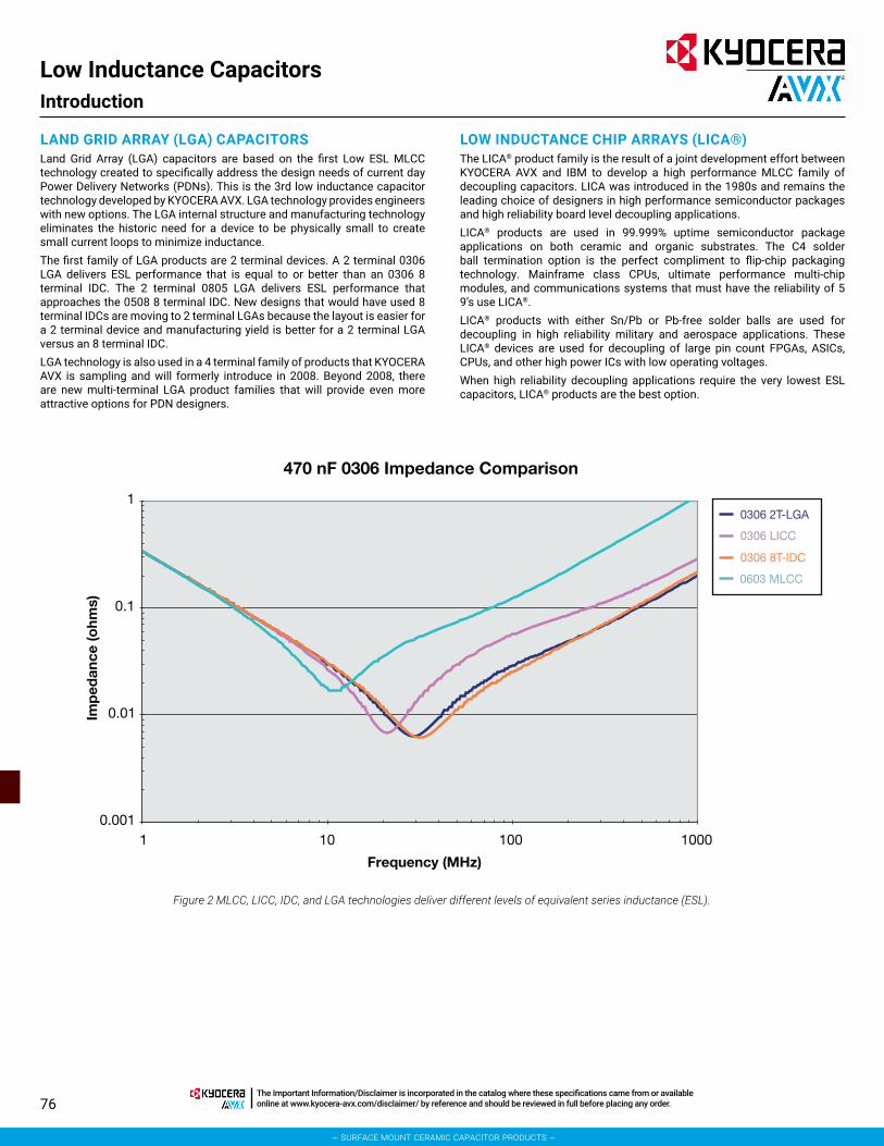
76
Low Inductance CapacitorsIntroduction
Figure 2 MLCC, LICC, IDC, and LGA technologies deliver different levels of equivalent series inductance (ESL).
LAND GRID ARRAY (LGA) CAPACITORSLand Grid Array (LGA) capacitors are based on the first Low ESL MLCC technology created to specifically address the design needs of current day Power Delivery Networks (PDNs). This is the 3rd low inductance capacitor technology developed by KYOCERA AVX. LGA technology provides engineers with new options. The LGA internal structure and manufacturing technology eliminates the historic need for a device to be physically small to create small current loops to minimize inductance.The first family of LGA products are 2 terminal devices. A 2 terminal 0306 LGA delivers ESL performance that is equal to or better than an 0306 8 terminal IDC. The 2 terminal 0805 LGA delivers ESL performance that approaches the 0508 8 terminal IDC. New designs that would have used 8 terminal IDCs are moving to 2 terminal LGAs because the layout is easier for a 2 terminal device and manufacturing yield is better for a 2 terminal LGA versus an 8 terminal IDC.LGA technology is also used in a 4 terminal family of products that KYOCERA AVX is sampling and will formerly introduce in 2008. Beyond 2008, there are new multi-terminal LGA product families that will provide even more attractive options for PDN designers.
LOW INDUCTANCE CHIP ARRAYS (LICA®)The LICA® product family is the result of a joint development effort between KYOCERA AVX and IBM to develop a high performance MLCC family of decoupling capacitors. LICA was introduced in the 1980s and remains the leading choice of designers in high performance semiconductor packages and high reliability board level decoupling applications.LICA® products are used in 99.999% uptime semiconductor package applications on both ceramic and organic substrates. The C4 solder ball termination option is the perfect compliment to flip-chip packaging technology. Mainframe class CPUs, ultimate performance multi-chip modules, and communications systems that must have the reliability of 5 9’s use LICA®.LICA® products with either Sn/Pb or Pb-free solder balls are used for decoupling in high reliability military and aerospace applications. These LICA® devices are used for decoupling of large pin count FPGAs, ASICs, CPUs, and other high power ICs with low operating voltages.When high reliability decoupling applications require the very lowest ESL capacitors, LICA® products are the best option.
470 nF 0306 Impedance Comparison
0.001
0.01
0.1
1
0001001011
Frequency (MHz)
Imp
edan
ce (o
hms)
0306 2T-LGA
0306 LICC
0306 8T-IDC
0603 MLCC
– surface mount ceramic capacitor products –
The Important Information/Disclaimer is incorporated in the catalog where these specifications came from or available online at www.kyocera-avx.com/disclaimer/ by reference and should be reviewed in full before placing any order.

77
Low Inductance Ceramic Capacitors0306/0508/0612 RoHS Compliant
GENERAL DESCRIPTIONThe key physical characteristic determining equivalent series inductance (ESL) of a capacitor is the size of the current loop it creates. The smaller the current loop, the lower the ESL.A standard surface mount MLCC is rectangular in shape with electrical terminations on its shorter sides. A Low Inductance Chip Capacitor (LICC) sometimes referred to as Reverse Geometry Capacitor (RGC) has its terminations on the longer sides of its rectangular shape. The image on the right shows the termination differences between an MLCC and an LICC.When the distance between terminations is reduced, the size of the current loop is reduced. Since the size of the current loop is the primary driver of inductance, an 0306 with a smaller current loop has significantly lower ESL then an 0603. The reduction in ESL varies by EIA size, however, ESL is typically reduced 60% or more with an LICC versus a standard MLCC.KYOCERA AVX LICC products are available with a lead-free finish of plated Nickel/Tin.
Capacitance Tolerances K = ±10%; M = ±20%
Operation Temperature Range
X7R = -55°C to +125°CX5R = -55°C to +85°C X7S = -55°C to +125°C
Temperature Coefficient X7R, X5R = ±15%; X7S = ±22%Voltage Ratings 4, 6.3, 10, 16, 25 VDC
Dissipation Factor4V, 6.3V = 6.5% max; 10V = 5.0% max;16V = 3.5% max; 25V = 3.0% max
Insulation Resistance(@+25°C, RVDC)
100,000MΩ min, or 1,000MΩ per μF min.,whichever is less
PERFORMANCE CHARACTERISTICS
MLCC LICC
HOW TO ORDER
0612 DZ M A 2 A*T105
DielectricC = X7RD = X5RW = X6SZ = X7S
Voltage4 = 4V
6 = 6.3VZ = 10VY = 16V3 = 25V5 = 50V
Capacitance ToleranceK = ±10%M = ±20%
Failure RateA = N/A
4 = Automotive**
Packaging Available
2 = 7" Reel4 = 13" Reel
Thickness Thickness
mm (in)0.56 (0.022)0.76 (0.030)1.02 (0.040)1.27 (0.050)
TerminationsT = Plated Ni
and Sn
Capacitance Code (In pF)2 Sig. Digits +
Number of Zeros
Size030605080612
*See the thickness tables on the next page. **Select voltages for Automotive version, contact factory NOTE: Contact factory for availability of Termination and Tolerance Options for Specific Part Numbers.
TYPICAL IMPEDANCE CHARACTERISTICS
LICC (Low Inductance Chip Capacitors)
081919
– surface mount ceramic capacitor products –
The Important Information/Disclaimer is incorporated in the catalog where these specifications came from or available online at www.kyocera-avx.com/disclaimer/ by reference and should be reviewed in full before placing any order.

78
Low Inductance Ceramic Capacitors0306/0508/0612 RoHS Compliant
SIZE 0306 0508 0612Packaging Embossed Embossed Embossed
Lengthmm 0.81 + 0.15 1.27 + 0.25 1.60 + 0.25(in.) (0.032 ± 0.006) (0.050 ± 0.010) (0.063 ± 0.010)
Width mm 1.60 + 0.15 2.00 + 0.25 3.20 + 0.25(in.) (0.063 ± 0.006) (0.080 ± 0.010) (0.126 ± 0.010)
Cap Code
WVDC 4 6.3 10 1 6 25 6.3 10 16 25 50 6.3 10 16 25 50
102 Cap 0.001 A A A A V V V V V S S S S V
222 (μF) .0022 A A A A S S S S V S S S S V
332 0.0033 A A A A S S S S V S S S S V
472 0.0047 A A A A S S S S V S S S S V
682 0.0068 A A A A S S S S V S S S S V
103 0.01 A A A A S S S S V S S S S V
153 0.015 A A A A S S S S V S S S S W
223 0.022 A A A A S S S S V S S S S W
333 0.033 A A A S S S V V S S S S W
473 0.047 A A A S S S V A S S S S W
683 0.068 A A A S S S A A S S S V W
104 0.1 A A A S S V A A S S S V W
154 0.15 A A S S V S S S W W
224 0.22 A A S S A S S V W
334 0.33 V V A S S V
474 0.47 V V A S S V
684 0.68 A A V V W
105 1 A A A V V A
155 1.5 A W W
225 2.2 A A
335 3.3 A
475 4.7
685 6.8
106 10
Solid = X7R = X5R = X7S = X6S
mm (in.) mm (in.) mm (in.)
0306Code Thickness
A 0.56 (0.022)
0508Code Thickness
S 0.56 (0.022)V 0.76 (0.030)A 1.02 (0.040)
0612Code Thickness
S 0.56 (0.022)V 0.76 (0.030)W 1.02 (0.040)A 1.27 (0.050)
PHYSICAL DIMENSIONS AND PAD LAYOUT
PHYSICAL DIMENSIONS
PAD LAYOUT DIMENSIONS
Size L W t
03060.81 ± 0.15 1.60 ± 0.15 0.13 min.
(0.032 ± 0.006) (0.063 ± 0.006) (0.005 min.)
05081.27 ± 0.25 2.00 ± 0.25 0.13 min.
(0.050 ± 0.010) (0.080 ± 0.010) (0.005 min.)
0612 1.60 ± 0.25 3.20 ± 0.25 0.13 min.(0.063 ± 0.010) (0.126 ± 0.010) (0.005 min.)
Size A B C0306 0.31 (0.012) 1.52 (0.060) 0.51 (0.020)0508 0.51 (0.020) 2.03 (0.080) 0.76 (0.030)0612 0.76 (0.030) 3.05 (0.120) 0.635 (0.025)
T - See Range Chart for Thickness and Codes
MM (IN.)
MM (IN.)
W t
T
L
“A” CC
“B”
LICC (Low Inductance Chip Capacitors)
051121
– surface mount ceramic capacitor products –
The Important Information/Disclaimer is incorporated in the catalog where these specifications came from or available online at www.kyocera-avx.com/disclaimer/ by reference and should be reviewed in full before placing any order.

79
Low Inductance Capacitors with SnPb TerminationsLD16/LD17/LD18 Tin-Lead Termination “B”
GENERAL DESCRIPTIONThe key physical characteristic determining equivalent series inductance (ESL) of a capacitor is the size of the current loop it creates. The smaller the current loop, the lower the ESL.A standard surface mount MLCC is rectangular in shape with electrical terminations on its shorter sides. A Low Inductance Chip Capacitor (LICC) sometimes referred to as Reverse Geometry Capacitor (RGC) has its terminations on the longer sides of its rectangular shape. The image on the right shows the termination differences between an MLCC and an LICC.When the distance between terminations is reduced, the size of the current loop is reduced. Since the size of the current loop is the primary driver of inductance, an 0306 with a smaller current loop has significantly lower ESL then an 0603. The reduction in ESL varies by EIA size, however, ESL is typically reduced 60% or more with an LICC versus a standard MLCC.AVX LICC products are available with a lead termination for high reliability military and aerospace applications that must avoid tin whisker reliability issues.
Capacitance Tolerances K = ±10%; M = ±20%
Operation Temperature Range
X7R = -55°C to +125°CX5R = -55°C to +85°C X7S = -55°C to +125°C
Temperature Coefficient X7R, X5R = ±15%; X7S = ±22%Voltage Ratings 4, 6.3, 10, 16, 25 VDC
Dissipation Factor4V, 6.3V = 6.5% max; 10V = 5.0% max;16V = 3.5% max; 25V = 3.0% max
Insulation Resistance(@+25°C, RVDC)
100,000MΩ min, or 1,000MΩ per μF min.,whichever is less
PERFORMANCE CHARACTERISTICS
MLCC LICC
HOW TO ORDER
LD18 DZ M A 2 A*B105
DielectricC = X7RD = X5RW = X6SZ = X7S
Voltage4 = 4V
6 = 6.3VZ = 10VY = 16V3 = 25V5 = 50V
Capacitance ToleranceK = ±10%M = ±20%
Failure RateA = N/A
Packaging Available
2 = 7" Reel4 = 13" Reel
Thickness Thickness
mm (in)0.56 (0.022)0.76 (0.030)1.02 (0.040)1.27 (0.050)
TerminationsB = 5% min lead
Capacitance Code (In pF)2 Sig. Digits +
Number of Zeros
SizeLD16 = 0306LD17 = 0508LD18 = 0612
*See the thickness tables on the next page.NOTE: Contact factory for availability of Termination and Tolerance Options for Specific Part Numbers.
TYPICAL IMPEDANCE CHARACTERISTICS
041416
– surface mount ceramic capacitor products –
The Important Information/Disclaimer is incorporated in the catalog where these specifications came from or available online at www.kyocera-avx.com/disclaimer/ by reference and should be reviewed in full before placing any order.

80
Low Inductance Capacitors with SnPb TerminationsLD16/LD17/LD18 Tin-Lead Termination “B”
SIZE LD16 (0306)
LD17 (0508)
LD18 (0612)
Packaging Embossed Embossed Embossed
Length mm 0.81 ± 0.15 1.27 ± 0.25 1.60 ± 0.25(in.) (0.032 ± 0.006) (0.050 ± 0.010) (0.063 ± 0.010)
Width mm 1.60 ± 0.15 2.00 ± 0.25 3.20 ± 0.25(in.) (0.063 ± 0.006) (0.080 ± 0.010) (0.126 ± 0.010)
Cap Code WVDC 6.3 10 1 6 25 6.3 10 16 25 50 6.3 10 16 25 50
102 Cap 0.001 A A A A S S S S V S S S S V
222 (μF) .0022 A A A A S S S S V S S S S V
332 0.0033 A A A A S S S S V S S S S V
472 0.0047 A A A A S S S S V S S S S V
682 0.0068 A A A A S S S S V S S S S V
103 0.01 A A A A S S S S V S S S S V
153 0.015 A A A A S S S S V S S S S W
223 0.022 A A A A S S S S V S S S S W
333 0.033 A A A S S S V V S S S S W
473 0.047 A A A S S S V A S S S S W
683 0.068 A A A S S S A A S S S V W
104 0.1 A A A S S V A A S S S V W
154 0.15 A A S S V S S S W W
224 0.22 A A S S A S S V W
334 0.33 V V A S S V
474 0.47 V V A S S V
684 0.68 A A V V W
105 1 A A V V A
155 1.5 A W W
225 2.2 A A
335 3.3 A
475 4.7
685 6.8
106 10
Solid = X7R = X5R = X6S
mm (in.) mm (in.) mm (in.)
LD16(0306)
Code ThicknessA 0.56 (0.022)
LD17(0508)
Code ThicknessS 0.56 (0.022)V 0.76 (0.030)A 1.02 (0.040)
LD18(0612)
Code ThicknessS 0.56 (0.022)V 0.76 (0.030)W 1.02 (0.040)A 1.27 (0.050)
PHYSICAL DIMENSIONS AND PAD LAYOUT
PHYSICAL DIMENSIONS
PAD LAYOUT DIMENSIONS
Size L W tLD16
(0306)0.81 ± 0.15 1.60 ± 0.15 0.13 min.
(0.032 ± 0.006) (0.063 ± 0.006) (0.005 min.)LD17
(0508)1.27 ± 0.25 2.00 ± 0.25 0.13 min.
(0.050 ± 0.010) (0.080 ± 0.010) (0.005 min.)LD18
(0612)1.60 ± 0.25 3.20 ± 0.25 0.13 min.
(0.063 ± 0.010) (0.126 ± 0.010) (0.005 min.)
Size A B CLD16
(0306) 0.31 (0.012) 1.52 (0.060) 0.51 (0.020)
LD17 (0508) 0.51 (0.020) 2.03 (0.080) 0.76 (0.030)
LD18 (0612) 0.76 (0.030) 3.05 (0.120) 0.635 (0.025)
T - See Range Chart for Thickness and Codes
MM (IN.)
MM (IN.)
W t
T
L
“A” CC
“B”
041416
– surface mount ceramic capacitor products –
The Important Information/Disclaimer is incorporated in the catalog where these specifications came from or available online at www.kyocera-avx.com/disclaimer/ by reference and should be reviewed in full before placing any order.

81
IDC Low Inductance Capacitors (RoHS)0306/0612/0508
GENERAL DESCRIPTIONInter-Digitated Capacitors (IDCs) are used for both semiconductor package and board level decoupling. The equivalent series inductance (ESL) of a single capacitor or an array of capacitors in parallel determines the response time of a Power Delivery Network (PDN). The lower the ESL of a PDN, the faster the response time. A designer can use many standard MLCCs in parallel to reduce ESL or a low ESL Inter-Digitated Capacitor (IDC) device. These IDC devices are available in versions with a maximum height of 0.95mm or 0.55mm.IDCs are typically used on packages of semiconductor products with power levels of 15 watts or greater. Inter-Digitated Capacitors are used on CPU, GPU, ASIC, and ASSP devices produced on 0.13μ, 90nm, 65nm, and 45nm processes. IDC devices are used on both ceramic and organic package substrates. These low ESL surface mount capacitors can be placed on the bottom side or the top side of a package substrate. The low profile 0.55mm maximum height IDCs can easily be used on the bottom side of BGA packages or on the die side of packages under a heat spreader.IDCs are used for board level decoupling of systems with speeds of 300MHz or greater. Low ESL IDCs free up valuable board space by reducing the number of capacitors required versus standard MLCCs. There are additional benefits to reducing the number of capacitors beyond saving board space including higher reliability from a reduction in the number of components and lower placement costs based on the need for fewer capacitors.The Inter-Digitated Capacitor (IDC) technology was developed by KYOCERA AVX. This is the second family of Low Inductance MLCC products created by KYOCERA AVX. IDCs are a cost effective alternative to KYOCERA AVX’s first generation low ESL family for high-reliability applications known as LICA (Low Inductance Chip Array).KYOCERA AVX IDC products are available with a lead-free finish of plated Nickel/Tin.
0612
0508
0306
+ – + –
+ – + –
TYPICAL IMPEDANCE
0.0010001001011
Frequency (MHz)
Impe
danc
e (O
hms)
0.01
0.1
1
10
LICC_0612
IDC_0612
MLCC_1206
Capacitance Tolerance ±20% Preferred
Operation Temperature Range
X7R = -55°C to +125°CX5R = -55°C to +85°C X7S = -55°C to +125°C
Temperature Coefficient ±15% (0VDC), ±22% (X7S)
Voltage Ratings 4, 6.3, 10, 16, 25 VDC
Dissipation Factor≤ 6.3V = 6.5% max; 10V = 5.0% max;≥ 16V = 3.5% max
Insulation Resistance(@+25°C, RVDC)
100,000MΩ min, or 1,000MΩ per μF min.,whichever is less
PERFORMANCE CHARACTERISTICS
HOW TO ORDER
D
DielectricC = X7RD = X5RZ = X7S
3
IDC Case Size
2 = 05083 = 06124 = 0306
1
Number of Terminals1 = 8 Termi-
nals
6
Voltage4 = 4V
6 = 6.3VZ = 10VY = 16V3 = 25V
M
Capacitance ToleranceM = ±20%
A
Failure Rate
A = N/A
3
PackagingAvailable1=7" Reel
3=13" Reel
A
ThicknessMax. Thickness
mm (in)A=Standard
S=0.55 (0.022)
T
TerminationT =Plated Ni
and Sn
225
Capacitance Code (In pF)2 Sig. Digits +
Number of Zeros
W
Style
L
Low Inductance
NOTE: Contact factory for availability of Termination and Tolerance Options for Specific Part Numbers.
Dissipation Factor No problems observed after 2.5 x RVDC for 5 seconds at 50mA max current
CTE (ppm/C) 12.0
Thermal Conductivity 4-5W/M K
Terminations Available Plated Nickel and Solder
IDC (InterDigitated Capacitors)
– surface mount ceramic capacitor products –
The Important Information/Disclaimer is incorporated in the catalog where these specifications came from or available online at www.kyocera-avx.com/disclaimer/ by reference and should be reviewed in full before placing any order.

82
IDC Low Inductance Capacitors (RoHS)
SIZE W4 = 0306 W2 = Thin 0508 W2 = 0508 W3= Thin 0612 W3 = 0612 W3 = THICK 0612Max. Thickness
mm 0.55 0.55. 0.95 0.55 0.95 1.22(in.) (0.022) (0.022) (0.037) (0.022) (0.037) (0.048)
WVDC 4 6.3 4 6.3 10 16 25 4 6.3 10 16 25 4 6.3 10 16 4 6.3 10 16 25 4 6.3 10 16Cap (μF) 0.010
0.0220.0330.0470.068
0.100.220.330.470.68
1.0 1.52.23.3
PHYSICAL DIMENSIONS AND PAD LAYOUT Consult factory foradditional requirements
= X7R
= X5R
= X7S
PHYSICAL CHIP DIMENSIONS MILLIMETERS (INCHES)
PAD LAYOUT DI-MENSIONS
SIZE W L BW BL P
03061.60 ± 0.20 0.82 ± 0.10 0.25 ± 0.10 0.20 ± 0.10 0.40 ± 0.05
(0.063 ± 0.008) (0.032 ± 0.006 (0.010 ± 0.004) (0.008± 0.004) (0.015 ± 0.002)
05082.03 ± 0.20 1.27 ± 0.20 0.30 ± 0.10 0.25 ± 0.15 0.50 ± 0.05
(0.080 ± 0.008) (0.050 ± 0.008) (0.012 ± 0.004) (0.010± 0.006) (0.020 ± 0.002)
0612 3.20 ± 0.20 1.60 ± 0.20 0.50 ± 0.10 0.25 ± 0.15 0.80 ± 0.10(0.126 ± 0.008) (0.063 ± 0.008) (0.020 ± 0.004) (0.010 ± 0.006) (0.031 ± 0.004)
SIZE A B C D E
0306 0.38(0.015)
0.89(0.035)
1.27(0.050)
0.20(0.008)
0.40(0.015)
0508 0.64(0.025)
1.27(0.050)
1.91(0.075)
0.28(0.011)
0.50(0.020)
0612 0.89(0.035)
1.65(0.065)
2.54(0.010)
0.45(0.018)
0.80(0.031)
0306/0612/0508IDC (InterDigitated Capacitors)
– surface mount ceramic capacitor products –
The Important Information/Disclaimer is incorporated in the catalog where these specifications came from or available online at www.kyocera-avx.com/disclaimer/ by reference and should be reviewed in full before placing any order.

83
IDC Low Inductance Capacitors (SnPb)
GENERAL DESCRIPTIONInter-Digitated Capacitors (IDCs) are used for both semiconductor package and board level decoupling. The equivalent series inductance (ESL) of a single capacitor or an array of capacitors in parallel determines the response time of a Power Delivery Network (PDN). The lower the ESL of a PDN, the faster the response time. A designer can use many standard MLCCs in parallel to reduce ESL or a low ESL Inter-Digitated Capacitor (IDC) device. These IDC devices are available in versions with a maximum height of 0.95mm or 0.55mm.
IDCs are typically used on packages of semiconductor products with power levels of 15 watts or greater. Inter-Digitated Capacitors are used on CPU, GPU, ASIC, and ASSP devices produced on 0.13μ, 90nm, 65nm, and 45nm processes. IDC devices are used on both ceramic and organic package substrates. These low ESL surface mount capacitors can be placed on the bottom side or the top side of a package substrate. The low profile 0.55mm maximum height IDCs can easily be used on the bottom side of BGA packages or on the die side of packages under a heat spreader.
IDCs are used for board level decoupling of systems with speeds of 300MHz or greater. Low ESL IDCs free up valuable board space by reducing the number of capacitors required versus standard MLCCs. There are additional benefits to reducing the number of capacitors beyond saving board space including higher reliability from a reduction in the number of components and lower placement costs based on the need for fewer capacitors.
The Inter-Digitated Capacitor (IDC) technology was developed by KYOCERA AVX. This is the second family of Low Inductance MLCC products created by KYOCERA AVX. IDCs are a cost effective alternative to KYOCERA AVX’s first generation low ESL family for high-reliability applications known as LICA (Low Inductance Chip Array).
KYOCERA AVX IDC products are available with a lead termination for high reliability military and aerospace applications that must avoid tin whisker reliability issues.
0612
0508
0306
+ – + –
+ – + –
TYPICAL IMPEDANCE
0.0010001001011
Frequency (MHz)
Impe
danc
e (O
hms)
0.01
0.1
1
10
LICC_0612
IDC_0612
MLCC_1206
Capacitance Tolerance ±20% Preferred
Operation Temperature Range
X7R = -55°C to +125°CX5R = -55°C to +85°C X7S = -55°C to +125°C
Temperature Coefficient ±15% (0VDC), ±22% (X7S)
Voltage Ratings 4, 6.3, 10, 16, 25 VDC
Dissipation Factor≤ 6.3V = 6.5% max; 10V = 5.0% max;≥ 16V = 3.5% max
Insulation Resistance(@+25°C, RVDC)
100,000MΩ min, or 1,000MΩ per μF min.,whichever is less
PERFORMANCE CHARACTERISTICS
HOW TO ORDER
D
DielectricC = X7RD = X5RZ = X7S
3
IDC Case Size
2 = 05083 = 06124 = 0306
1
Number of Terminals1 = 8 Termi-
nals
6
Voltage4 = 4V
6 = 6.3VZ = 10VY = 16V3 = 25V
M
Capacitance ToleranceM = ±20%
A
Failure Rate
A = N/A
3
PackagingAvailable1=7" Reel
3=13" Reel
A
ThicknessMax. Thickness
mm (in)A=Standard
S=0.55 (0.022)
B
TerminationB =5% min.
Lead
225
Capacitance Code (In pF)2 Sig. Digits +
Number of Zeros
L
Style
L
Low Inductance
NOTE: Contact factory for availability of Termination and Tolerance Options for Specific Part Numbers.
Dissipation Factor No problems observed after 2.5 x RVDC for 5 seconds at 50mA max current
CTE (ppm/C) 12.0
Thermal Conductivity 4-5W/M K
Terminations Available Plated Nickel and Solder
0306/0612/0508IDC (InterDigitated Capacitors)
012820
– surface mount ceramic capacitor products –
The Important Information/Disclaimer is incorporated in the catalog where these specifications came from or available online at www.kyocera-avx.com/disclaimer/ by reference and should be reviewed in full before placing any order.

84
IDC Low Inductance Capacitors (SnPb)
SIZE W4 = 0306 W2 = Thin 0508 W2 = 0508 W3= Thin 0612 W3 = 0612 W3 = THICK 0612Max. Thickness
mm 0.55 0.55. 0.95 0.55 0.95 1.22(in.) (0.022) (0.022) (0.037) (0.022) (0.037) (0.048)
WVDC 4 6.3 4 6.3 10 16 25 4 6.3 10 16 25 4 6.3 10 16 4 6.3 10 16 25 4 6.3 10 16
Cap(μF) 0.010
0.022
0.033
0.047
0.068
0.10
0.22
0.33
0.47
0.68
1.0
1.5
2.2
3.3
PHYSICAL DIMENSIONS AND PAD LAYOUT Consult factory foradditional requirements
= X7R
= X5R
= X7S
PHYSICAL CHIP DIMENSIONS MILLIMETERS (INCHES)
PAD LAYOUT DI-MENSIONS
SIZE W L BW BL P
03061.60 ± 0.20 0.82 ± 0.10 0.25 ± 0.10 0.20 ± 0.10 0.40 ± 0.05
(0.063 ± 0.008) (0.032 ± 0.006 (0.010 ± 0.004) (0.008± 0.004) (0.015 ± 0.002)
05082.03 ± 0.20 1.27 ± 0.20 0.30 ± 0.10 0.25 ± 0.15 0.50 ± 0.05
(0.080 ± 0.008) (0.050 ± 0.008) (0.012 ± 0.004) (0.010± 0.006) (0.020 ± 0.002)
0612 3.20 ± 0.20 1.60 ± 0.20 0.50 ± 0.10 0.25 ± 0.15 0.80 ± 0.10(0.126 ± 0.008) (0.063 ± 0.008) (0.020 ± 0.004) (0.010 ± 0.006) (0.031 ± 0.004)
SIZE A B C D E
0306 0.38(0.015)
0.89(0.035)
1.27(0.050)
0.20(0.008)
0.40(0.015)
0508 0.64(0.025)
1.27(0.050)
1.91(0.075)
0.28(0.011)
0.50(0.020)
0612 0.89(0.035)
1.65(0.065)
2.54(0.010)
0.45(0.018)
0.80(0.031)
0306/0612/0508IDC (InterDigitated Capacitors) with Sn/Pb Termination
– surface mount ceramic capacitor products –
The Important Information/Disclaimer is incorporated in the catalog where these specifications came from or available online at www.kyocera-avx.com/disclaimer/ by reference and should be reviewed in full before placing any order.

85
LGA Low Inductance Capacitors0204/0306 Land Grid Array
Land Grid Array (LGA) capacitors are the latest family of low inductance MLCCs from KYOCERA AVX. These new LGA products are the third low inductance family developed by KYOCERA AVX. The innovative LGA technology sets a new standard for low inductance MLCC performance.Our initial 2 terminal versions of LGA technology deliver the performance of an 8 terminal IDC low inductance MLCC with a number of advantages including:• Simplified layout of 2 large solder pads compared to 8 small pads for IDCs• Opportunity to reduce PCB or substrate contribution to system ESL by using multiple parallel vias in
solder pads• Advanced FCT manufacturing process used to create uniformly flat terminations on the capacitor
that resist “tombstoning”• Better solder joint reliability
APPLICATIONS
Semiconductor Packages• Microprocessors/CPUs• Graphics Processors/GPUs• Chipsets• FPGAs• ASICs
Board Level Device Decoupling• Frequencies of 300 MHz or more• ICs drawing 15W or more• Low voltages• High speed buses
0306 2 TERMINAL LGA COMPARISON WITH 0306 8 TERMINAL IDC
0.001
0.01
0.1
1
1 10 100 1000
Frequency (MHz)
Imp
edan
ce (Ω
)
051316
– surface mount ceramic capacitor products –
The Important Information/Disclaimer is incorporated in the catalog where these specifications came from or available online at www.kyocera-avx.com/disclaimer/ by reference and should be reviewed in full before placing any order.

86
LGA Low Inductance Capacitors0204/0306 Land Grid Array
SIZE LG12 (0204) LG22 (0306)Length mm (in.) 0.50 (0.020) 0.76 (0.030)Width mm (in.) 1.00 (0.039) 1.60 (0.063)Temp. Char. X5R (D) X7S (Z) X6S (W) X7R (C) X5R (D) X7S (Z) X6S (W)Working Voltage 6.3 4 6.3 4 6.3 4 10 6.3 4 6.3 4 6.3 4 6.3 4
(6) (4) (6) (4) (6) (4) (Z) (6) (4) (6) (4) (6) (4) (6) (4)Cap (μF) 0.010 (103)
0.022 (223)0.047 (473)0.100 (104)0.220 (224)0.330 (334)0.470 (474)1.000 (105)2.200 (225)
= X7R = X5R = X7S = X6S
LG 2 1041 6 Z AM T S 12
Coded Cap
Case Size
1 = 02042 = 0306
Working Voltage4 = 4V6 = 6.3VZ = 10V
Temperature Characteristic
C = X7RD = X5RZ = X7SW = X6S
Termination Style
A = “U” Land
Cap ToleranceM = ±20%
Termination100% Sn*
*Contact factory for other termination
finishes
Thickness S = 0.55mm
max
Number of Capacitors
Packaging Tape & Reel2 = 7" Reel4 = 13" Reel
Style Number ofTerminals
2
HOW TO ORDER
PART DIMENSIONS MM (INCHES)
RECOMMENDED SOLDER PAD DIMENSIONS MM (INCHES)
T
L
BL
W
BW
L
BL
Reverse Geometry LGA
LG12, LG22
Top View
Side 1Side 2
PL
G
PW1
Series L W T BW BL
LG12 (0204) 0.5 ± 0.05(0.020±0.002)
1.00 ± 0.10(0.039 ± 0.004)
0.50 ± 0.05(0.020 ± 0.002)
0.8 ± 0.10(0.031 ± 0.004)
0.13 ± 0.08(0.005 ± 0.003)
LG22 (0306) 0.76 ± 0.10(0.030 ± 0.004)
1.60 ± 0.10(0.063 ± 0.004)
0.50 ± 0.05(0.020 ± 0.002)
1.50 ±0.10(0.059 ± 0.004)
0.28 ± 0.08(0.011 ± 0.003)
Series PL PW1 GLG12 (0204) 0.50 (0.020) 1.00 (0.039) 0.20 (0.008)LG22 (0306) 0.65 (0.026) 1.50 (0.059) 0.20 (0.008)
051316
– surface mount ceramic capacitor products –
The Important Information/Disclaimer is incorporated in the catalog where these specifications came from or available online at www.kyocera-avx.com/disclaimer/ by reference and should be reviewed in full before placing any order.

87
LGA Low Inductance Capacitors0204/0306 Land Grid Array – Tin/Lead Termination “B”
SIZE PG12 (0204) PG22 (0306)Length mm (in.) 0.50 (0.020) 0.76 (0.030)Width mm (in.) 1.00 (0.039) 1.60 (0.063)Temp. Char. X5R (D) X7S (Z) X6S (W) X7R (C) X5R (D) X7S (Z) X6S (W)Working Voltage 6.3 4 6.3 4 6.3 4 10 6.3 4 6.3 4 6.3 4 6.3 4
(6) (4) (6) (4) (6) (4) (Z) (6) (4) (6) (4) (6) (4) (6) (4)Cap (μF) 0.010 (103)
0.022 (223)0.047 (473)0.100 (104)0.220 (224)0.330 (334)0.470 (474)1.000 (105)2.200 (225)
= X7R = X5R = X7S = X6S
PG 2 1041 6 Z AM B S 12
Coded Cap
Case Size
1 = 02042 = 0306
Working Voltage4 = 4V6 = 6.3VZ = 10V
Temperature Characteristic
C = X7RD = X5RZ = X7SW = X6S
Termination Style
A = “U” Land
Cap ToleranceM = ±20%
Termination5% Min Lead
Thickness S = 0.55mm
max
Number of Capacitors
Packaging Tape & Reel2 = 7" Reel4 = 13" Reel
Style Number ofTerminals
2
HOW TO ORDER
PART DIMENSIONS MM (INCHES)
RECOMMENDED SOLDER PAD DIMENSIONS MM (INCHES)
PL
G
PW1
Series L W T BW BL
PG12 (0204) 0.5 ± 0.05(0.020±0.002)
1.00 ± 0.10(0.039 ± 0.004)
0.50 ± 0.05(0.020 ± 0.002)
0.8 ± 0.10(0.031 ± 0.004)
0.13 ± 0.08(0.005 ± 0.003)
PG22 (0306) 0.76 ± 0.10(0.030 ± 0.004)
1.60 ± 0.10(0.063 ± 0.004)
0.50 ± 0.05(0.020 ± 0.002)
1.50 ±0.10(0.059 ± 0.004)
0.28 ± 0.08(0.011 ± 0.003)
Series PL PW1 GPG12 (0204) 0.50 (0.020) 1.00 (0.039) 0.20 (0.008)PG22 (0306) 0.65 (0.026) 1.50 (0.059) 0.20 (0.008)
T
L
BL
W
BW
L
BL
Reverse Geometry LGA
LG12, LG22
Top View
Side 1Side 2
ReverseGeometry LGA
PG12, PG22
051316
– surface mount ceramic capacitor products –
The Important Information/Disclaimer is incorporated in the catalog where these specifications came from or available online at www.kyocera-avx.com/disclaimer/ by reference and should be reviewed in full before placing any order.

88
High Temperature MLCCsAT Series – 200ºC & 250°C Rated
080416
Present military specifications, as well as a majority of commercial applications, require a maximum operating temperature of 125°C. However, the emerging market for high temperature electronics demands capacitors operating reliably at temperatures beyond 125°C. KYOCERA AVX’s high temperature chip capacitor product line, has been extended with the BME C0G chip. All AT chips have verified capabilities of long term operation up to 250°C for applications in both military and commercial businesses. These capacitors demonstrate high volumetric efficiency, high insulation resistance and low ESR/ESL for the most demanding applications, such as “down-hole” oil exploration and aerospace programs.
HOW TO ORDER
ELECTRICAL SPECIFICATIONS
AT10 1043 K A 2 ATT
StyleAT03 = 0603AT05 = 0805AT06 = 1206AT10 = 1210AT12 = 1812AT14 = 2225
Capacitance Code(2 significant digits
+ no. of zeros)101 = 100pF102 = 1nF103 = 10nF104 = 100nF105 = 1μF
Voltage Code
16V = Y25V = 350V = 5
CapacitanceTolerance
J = ±5%K = ±10%M = ±20%
Test LevelA = Standard
Packaging2 = 7" Reel4 = 13" Reel9 = Bulk
Special Code
A = Standard
Termination1 = Pd/AgT = 100% Sn Plated
(RoHS Compliant)7 = Ni/Au Plated
(For 250°C BME C0G Only)
Temperature Coefficient
PMEC0G 250°C = AC0G 200°C = 2VHT 250°C = TVHT 200°C = 4
BMEC0G 250°C = 5C0G 200°C = 3
DIMENSIONS: MILLIMETERS (INCHES)
Temperature CoefficientPME C0G 0±30ppm/°C, -55C to 250°C BME C0G 0±30ppm/°C, -55C to 200°C
See TCC Plot for +250°CVHT: T ±15%, -55°C to +150°C
See TCC Plot for +250°CCapacitance Test (MIL-STD-202, Method 305) 25°C, 1.0 ± 0.2 Vrms (open circuit voltage) @ 1kHzDissipation factor 25°C C0G: 0.15% Max at 1.0 ± 0.2 Vrms (open circuit voltage) @ 1kHz VHT: 2.5% Max at 1.0 ± 0.2 Vrms (open circuit voltage) @ 1kHz
Insulation Resistance 25°C (MIL-STD-202, Method 302) 100GΩ or 1000MΩ-μF (whichever is less)Insulation Resistance 125°C (MIL-STD-202, Method 302) 10GΩ or 100MΩ-μF (whichever is less)Insulation Resistance 200°C (MIL-STD-202, Method 302) 1GΩ or 10MΩ-μF (whichever is less)Insulation Resistance 250°C (MIL-STD-202, Method 302) 100MΩ or 1MΩ-μF (whichever is less)Direct Withstanding Voltage 25°C (Flash Test) 250% rated voltage for 5 seconds with 50mA max charging current
Size AT03 = 0603 AT05= 0805 AT06=1206 AT10=1210 AT12=1812 AT14=2225
(L) Length 1.60 ± 0.15 (0.063 ± 0.006)
2.01 ± 0.20 (0.079 ± 0.008)
3.20 ± 0.20 (0.126 ± 0.008)
3.20 ± 0.20 (0.126 ± 0.008)
4.50 ± 0.30 (0.177 ± 0.012)
5.72 ± 0.25 (0.225 ± 0.010)
(W) Width 0.81 ± 0.15(0.032 ± 0.006)
1.25 ± 0.20(0.049 ± 0.008)
1.60 ± 0.20(0.063 ± 0.008)
2.50 ± 0.20(0.098 ± 0.008)
3.20 ± 0.20(0.126 ± 0.008)
6.35 ± 0.25(0.250 ± 0.010)
(T) Thickness Max. 1.02 (0.040)
1.30 (0.051)
1.52 (0.060)
1.70(0.067)
2.54(0.100)
2.54(0.100)
(t) terminal
min.max.
0.25 (0.010)0.75 (0.030)
0.25 (0.010)0.75 (0.030)
0.25 (0.010)0.75 (0.030)
0.25 (0.010)0.75 (0.030)
0.25 (0.010)1.02 (0.040)
0.25 (0.010)1.02 (0.040)
– surface mount ceramic capacitor products –
The Important Information/Disclaimer is incorporated in the catalog where these specifications came from or available online at www.kyocera-avx.com/disclaimer/ by reference and should be reviewed in full before placing any order.

89080416
High Temperature MLCCAT Series – 200ºC & 250°C Rated
PERFORMANCE CHARACTERISTICS
-100
-71.25
-42.5
-13.75
15
-50 -25 0 25 50 75 100 125 150 175 200 225 250
C (
%)
Temperature (°C)
-20
-15
-10
-5
0
5
0 10 20 30 40 50 60 70 80 90 100
C (
%)
Percentage of Rated Voltage
16VDC25VDC50VDC100VDC200VDC
Legend:Capacitor’s Rated Voltage
-1
-0.8
-0.6
-0.4
-0.2
0
0.2
0.4
0.6
0.8
1
0 10 20 30 40 50 60 70 80 90 100
C (
%)
Percentage of Rated Voltage
1
10
100
1000
10000
25 50 75 100 125 150 175 200 225 250
RC (Ω
*F)
Temperature (°C)
1
10
100
1000
1000000
10000
100000
25 50 75 100 125 150 175 200 225 250
RC (Ω
*F)
Temperature (°C)
Typical Temperature Coefcient of Capacitance (VHT Dielectric) Typical Temperature Coefcient of Capacitance (C0G Dielectric)
Typical Voltage Coefcient of Capacitance (VHT Dielectric) Typical Voltage Coefcient of Capacitance (C0G Dielectric)
Typical RC vs Temperature (VHT Dielectric) Typical RC vs Temperature (C0G Dielectric)
-1
-0.5
0
0.5
1
1.5
-50 -25 0 25 50 75 100 125 150 175 200 225 250
-30ppm/°C
+30ppm/°C
PME
BME
C (
%)
Temperature (°C)
– surface mount ceramic capacitor products –
The Important Information/Disclaimer is incorporated in the catalog where these specifications came from or available online at www.kyocera-avx.com/disclaimer/ by reference and should be reviewed in full before placing any order.

90
High Temperature MLCCAT Series – 200ºC & 250°C Rated
RELIABILITY
FREQUENCY RESPONSE
0
12000
24000
36000
48000
0 250 500 750 1000
250°C Life Test @ 2x Rated Voltage (C0G Dielectric)
Ca
pa
cit
an
ce
(p
F)
Time (hrs)
AT143A473AT123A123
0
0.275
0.55
0.825
1.1
0 250 500 750 1000
250°C Life Test @ 2x Rated Voltage (VHT Dielectric)
Ca
pa
cit
an
ce
(F
)
Time (hrs)
AT05YT104AT103T104AT123T334AT143T105
1E-02
1E-01
1E+00
1E+01
1E+02
1E+03
1E+01 1E+02 1E+03 1E+04 1E+05 1E+06 1E+07 1E+08
ESR Frequency Response (VHT Dielectric)
ES
R (
)
Frequency (Hz)
AT05YT104AT123T334AT143T105
1E-03
1E-02
1E-01
1E+00
1E+01
1E+02
1E+03
1E+01 1E+02 1E+03 1E+04 1E+05 1E+06 1E+07 1E+08
ESR Frequency Response (C0G Dielectric)
ES
R (
)
Frequency (Hz)
AT143A473AT123A123
1E-02
1E-01
1E+00
1E+01
1E+02
1E+03
1E+04
1E+05
1E+01 1E+02 1E+03 1E+04 1E+05 1E+06 1E+07 1E+08
Impedance Frequency Response (VHT Dielectric)
Imp
ed
an
ce
()
Frequency (Hz)
AT05YT104AT123T334AT143T105
1E-02
1E-01
1E+00
1E+01
1E+02
1E+03
1E+04
1E+05
1E+06
1E+01 1E+02 1E+03 1E+04 1E+05 1E+06 1E+07 1E+08
Impedance Frequency Response (C0G Dielectric)
Imp
ed
an
ce
()
Frequency (Hz)
AT143A473AT123A123
VHT - Failure Rate @ 90% Confidence Level (%/1000 hours)Temperature (°C) 50% Rated Voltage 100% Rated Voltage
200 0.002 0.017250 0.026 0.210
C0G - Failure Rate @ 90% Confidence Level (%/1000 hours)Temperature (°C) 50% Rated Voltage 100% Rated Voltage
200 0.006 0.047250 0.074 0.590
*Typical 1210, 1812, 2225 Failure Rate Analysis based on 250°C testing and voltage ratings specified on the following page.
*Typical 1812 and 2225 Failure Rate Analysis based on 250°C testing and voltage ratings specified on the following page.
080416
– surface mount ceramic capacitor products –
The Important Information/Disclaimer is incorporated in the catalog where these specifications came from or available online at www.kyocera-avx.com/disclaimer/ by reference and should be reviewed in full before placing any order.

91
High Temperature MLCCAT Series – 200ºC & 250°C Rated
Case Size AT03 = 0603
AT05 = 0805
AT06 = 1206
AT10 = 1210
AT12 = 1812
AT14 = 2225
Soldering Reflow/Wave Reflow/Wave Reflow/Wave Reflow Only Reflow Only Reflow Only
(L) Lengthmm 1.60 ± 0.15 2.01 ± 0.20 3.20 ± 0.20 3.20 ± 0.20 4.50 ± 0.30 5.72 ± 0.25(in.) (0.063 ± 0.006) (0.079 ± 0.008) (0.126 ± 0.008) (0.126 ± 0.008) (0.177 ± 0.012) (0.225 ± 0.010)
(W) Widthmm 0.81 ± 0.15 1.25 ± 0.20 1.60 ± 0.20 2.50 ± 0.20 3.20 ± 0.20 6.35 ± 0.25(in.) (0.032 ± 0.006) (0.049 ± 0.008) (0.063 ± 0.008) (0.098 ± 0.008) (0.126 ± 0.008) (0.250 ± 0.010)
(T) Thicknessmm 1.02 1.30 1.52 1.70 2.54 2.54(in.) (0.040) (0.051) (0.060) (0.067) (0.100) (0.100)
(t) Terminalmin 0.25 (0.010) 0.25 (0.010) 0.25 (0.010) 0.25 (0.010) 0.25 (0.010) 0.25 (0.010)max 0.75 (0.030) 0.75 (0.030) 0.75 (0.030) 0.75 (0.030) 1.02 (0.040) 1.02 (0.040)
Rated Temp. (ºC) 200 200 200 200 200 200Temp. Coefficeint 4 4 4 4 4 4
Voltage (V) 25 25 50 25 50 25 50 50 50
Cap (pF)
1000 1021200 1221500 1521800 1822200 2222700 2723300 3323900 3924700 4725600 5626800 6828200 822
Cap (μF)
0.010 1030.012 1230.015 1530.018 1830.022 2230.027 2730.033 3330.039 3930.047 4730.056 5630.068 6830.082 8230.100 1040.120 1240.150 1540.180 1840.220 2240.270 2740.330 3340.390 3940.470 4740.560 5640.680 6840.820 8241.000 105
Voltage (V) 25 25 50 25 50 25 50 50 50Rated Temp. (ºC) 200 200 200 200 200 200
Case Size AT03 = 0603
AT05 = 0805
AT06 = 1206
AT10 = 1210
AT12 = 1812
AT14 = 2225
Case Size AT03 = 0603
AT05 = 0805
AT06 = 1206
AT10 = 1210
AT12 = 1812
AT14 = 2225
Soldering Reflow/Wave Reflow/Wave Reflow/Wave Reflow Only Reflow Only Reflow Only
(L) Lengthmm 1.60 ± 0.15 2.01 ± 0.20 3.20 ± 0.20 3.20 ± 0.20 4.50 ± 0.30 5.72 ± 0.25(in.) (0.063 ± 0.006) (0.079 ± 0.008) (0.126 ± 0.008) (0.126 ± 0.008) (0.177 ± 0.012) (0.225 ± 0.010)
(W) Widthmm 0.81 ± 0.15 1.25 ± 0.20 1.60 ± 0.20 2.50 ± 0.20 3.20 ± 0.20 6.35 ± 0.25(in.) (0.032 ± 0.006) (0.049 ± 0.008) (0.063 ± 0.008) (0.098 ± 0.008) (0.126 ± 0.008) (0.250 ± 0.010)
(T) Thicknessmm 1.02 1.30 1.52 1.70 2.54 2.54(in.) (0.040) (0.051) (0.060) (0.067) (0.100) (0.100)
(t) Terminalmin 0.25 (0.010) 0.25 (0.010) 0.25 (0.010) 0.25 (0.010) 0.25 (0.010) 0.25 (0.010)max 0.75 (0.030) 0.75 (0.030) 0.75 (0.030) 0.75 (0.030) 1.02 (0.040) 1.02 (0.040)
Rated Temp. (ºC) 250 250 250 250 250 250Temp. Coefficeint T T T T T T
Voltage (V) 16 16 25 16 25 16 25 25 25
Cap (pF)
1000 1021200 1221500 1521800 1822200 2222700 2723300 3323900 3924700 4725600 5626800 6828200 822
Cap (μF)
0.010 1030.012 1230.015 1530.018 1830.022 2230.027 2730.033 3330.039 3930.047 4730.056 5630.068 6830.082 8230.100 1040.120 1240.150 1540.180 1840.220 2240.270 2740.330 3340.390 3940.470 4740.560 5640.680 6840.820 8241.000 105
Voltage (V) 16 16 25 16 25 16 25 25 25Rated Temp. (ºC) 250 250 250 250 250 250
Case Size AT03 = 0603
AT05 = 0805
AT06 = 1206
AT10 = 1210
AT12 = 1812
AT14 = 2225
CAPACITANCE RANGEPREFERRED SIZES ARE SHADED
VHT VHTTemp. Coefficient: 4 Temp. Coefficient: T200ºC Rated 250ºC Rated
Voltage rating per table. Capacitance values specified at 25ºC, derate capacitance value based on TCC and VCC Plots on page 107.NOTE: Contact factory for non-specified capacitance values.
080416
– surface mount ceramic capacitor products –
The Important Information/Disclaimer is incorporated in the catalog where these specifications came from or available online at www.kyocera-avx.com/disclaimer/ by reference and should be reviewed in full before placing any order.

92
High Temperature MLCCAT Series – 200ºC & 250°C Rated
Case Size AT03=0603 AT05=0805 AT06=1206
Soldering Reflow/Wave Reflow/Wave Reflow/Wave
(L) Length mm 1.60 ± 0.15 2.01 ± 0.20 3.20 ± 0.20(in.) (0.063 ± 0.006) (0.079 ± 0.008) (0.126 ± 0.008)
(W) Width mm 0.81 ± 0.15 1.25 ± 0.20 1.60 ± 0.20(in.) (0.032 ± 0.006) (0.049 ± 0.008) (0.063 ± 0.008)
(T) Thickness mm 1.02 1.30 1.52(in.) (0.040) (0.051) (0.060)
(t) Terminal min 0.25 (0.010) 0.25(0.010) 0.25 (0.010)max 0.75(0.030) 0.75(0.030) 0.75 (0.030)
Rated Temp. (ºC) 200 200 200Temp.
Coefficeint3 3 3
Voltage (V) 25 50 25 50 25 50Cap (pF)
39 39047 47056 56068 68082 820100 101120 121150 151180 181220 221270 271330 331390 391470 471560 561680 681820 8211000 1021200 1221500 1521800 1822200 2222700 2723300 3323900 3924700 4725600 5626800 6828200 822
Cap (μF)
0.010 1030.012 1230.015 1530.018 1830.022 2230.027 2730.033 3330.039 3930.047 4730.056 5630.068 6830.082 8230.100 104
Voltage (V) 25 50 25 50 25 50
Rated Temp. (ºC) 200 200 200 200 200 200
Case Size AT03=0603 AT05=0805 AT06=1206
Case Size AT03=0603 AT05=0805 AT06 = 1206
Soldering Reflow/Wave Reflow/Wave Reflow/Wave
(L) Length mm 1.60 ± 0.15 2.01 ± 0.20 3.20 ± 0.20(in.) (0.063 ± 0.006) (0.079 ± 0.008) (0.126 ± 0.008)
(W) Width mm 0.81 ± 0.15 1.25 ± 0.20 1.60 ± 0.20(in.) (0.032 ± 0.006) (0.049 ± 0.008) (0.063 ± 0.008)
(T) Thickness
mm 1.02 1.30 1.52(in.) (0.040) (0.051) (0.060)
(t) Terminal
min 0.25 (0.010) 0.25(0.010) 0.25 (0.010)max 0.75 (0.030) 0.75(0.030) 0.75 (0.030)
Rated Temp. (ºC) 250 250 250Temp.
Coefficeint5 5 5
Voltage (V) 25 25 25Cap (pF)
39 39047 47056 56068 68082 820100 101120 121150 151180 181220 221270 271330 331390 391470 471560 561680 681820 8211000 1021200 1221500 1521800 1822200 2222700 2723300 3323900 3924700 4725600 5626800 6828200 822
Cap (μF)
0.010 1030.012 1230.015 1530.018 1830.022 2230.027 2730.033 3330.039 3930.047 4730.056 5630.068 6830.082 8230.100 104
Voltage (V) 25 25 25
Rated Temp. (ºC) 250 250 250
Case Size AT03=0603 AT05=0805 AT06=1206
CAPACITANCE RANGEPREFERRED SIZES ARE SHADED
BME C0G BME C0G (Ni/Au)Temp. Coefficient: 4 Temp. Coefficient: 5200ºC Rated 250ºC Rated
Voltage rating per table. Capacitance values specified at 25ºC, derate capacitance value based on TCC and VCC Plots on page 107.NOTE: Contact factory for non-specified capacitance values.
080416
– surface mount ceramic capacitor products –
The Important Information/Disclaimer is incorporated in the catalog where these specifications came from or available online at www.kyocera-avx.com/disclaimer/ by reference and should be reviewed in full before placing any order.

93
Case Size AT05 = 0805 AT06 = 1206 AT10 = 1210 AT12 = 1812 AT14 = 2225Soldering Reflow/Wave Reflow/Wave Reflow Only Reflow Only Reflow Only
(L) Lengthmm 2.01 ± 0.20 3.20 ± 0.20 3.20 ± 0.20 4.50 ± 0.30 2.75 ± 0.25(in.) (0.079 ± 0.008) (0.126 ± 0.008) (0.126 ± 0.008) (0.177 ± 0.012) (0.225 ± 0.010)
(W) Widthmm 1.25 ± 0.20 1.60 ± 0.20 2.50 ± 0.20 3.20 ± 0.20 6.35 ± 0.25(in.) (0.049 ± 0.008) (0.063 ± 0.008) (0.098 ± 0.008) (0.126 ± 0.008) (0.250 ± 0.010)
(T) Thicknessmm 1.30 1.52 1.70 2.54 2.54(in.) (0.051) (0.060) (0.067) (0.100) (0.100)
(t) Terminalmin 0.25 (0.010) 0.25 (0.010) 0.25 (0.010) 0.25 (0.010) 0.25 (0.010)max 0.75 (0.030) 0.75 (0.030) 0.75 (0.030) 1.02 (0.040) 1.02 (0.040)
Rated Temp. (ºC) 200 200 200 200 200
Temp. Coefficeint 2 2 2 2 2Voltage (V) 50 50 50 50 50
Cap (pF)
100 101120 121150 151180 181220 221270 271330 331390 391470 471560 561680 681820 821
1000 1021200 1221500 1521800 1822200 2222700 2723300 3323900 3924700 4725600 5626800 6828200 822
Cap (μF)
0.010 1030.012 1230.015 1530.018 1830.022 2230.027 2730.033 3330.039 3930.047 4730.056 5630.068 6830.082 8230.100 104
Voltage (V) 50 50 50 50 50Rated Temp. (ºC) 200 200 200 200 200
Case Size AT05 = 0805 AT06 = 1206 AT10 = 1210 AT12 = 1812 AT14 = 2225
Case Size AT05 = 0805 AT06 = 1206 AT10 = 1210 AT12 = 1812 AT14 = 2225Soldering Reflow/Wave Reflow/Wave Reflow Only Reflow Only Reflow Only
(L) Lengthmm 2.01 ± 0.20 3.20 ± 0.20 3.20 ± 0.20 4.50 ± 0.30 2.75 ± 0.25(in.) (0.079 ± 0.008) (0.126 ± 0.008) (0.126 ± 0.008) (0.177 ± 0.012) (0.225 ± 0.010)
(W) Widthmm 1.25 ± 0.20 1.60 ± 0.20 2.50 ± 0.20 3.20 ± 0.20 6.35 ± 0.25(in.) (0.049 ± 0.008) (0.063 ± 0.008) (0.098 ± 0.008) (0.126 ± 0.008) (0.250 ± 0.010)
(T) Thicknessmm 1.30 1.52 1.70 2.54 2.54(in.) (0.051) (0.060) (0.067) (0.100) (0.100)
(t) Terminalmin 0.25 (0.010) 0.25 (0.010) 0.25 (0.010) 0.25 (0.010) 0.25 (0.010)max 0.75 (0.030) 0.75 (0.030) 0.75 (0.030) 1.02 (0.040) 1.02 (0.040)
Rated Temp. (ºC) 250 250 250 250 250
Temp. Coefficeint A A A A AVoltage (V) 25 25 25 25 25
Cap (pF)
100 101120 121150 151180 181220 221270 271330 331390 391470 471560 561680 681820 821
1000 1021200 1221500 1521800 1822200 2222700 2723300 3323900 3924700 4725600 5626800 6828200 822
Cap (μF)
0.010 1030.012 1230.015 1530.018 1830.022 2230.027 2730.033 3330.039 3930.047 4730.056 5630.068 6830.082 8230.100 104
Voltage (V) 25 25 25 25 25Rated Temp. (ºC) 250 250 250 250 250
Case Size AT05 = 0805 AT06 = 1206 AT10 = 1210 AT12 = 1812 AT14 = 2225
CAPACITANCE RANGEPREFERRED SIZES ARE SHADED
PME C0G PME C0GTemp. Coefficient: 2 Temp. Coefficient: A200ºC Rated 250ºC Rated
Voltage rating per table. Capacitance values specified at 25ºC, derate capacitance value based on TCC and VCC Plots on page 107.NOTE: Contact factory for non-specified capacitance values.
High Temperature MLCCAT Series – 200ºC & 250°C Rated
080416
– surface mount ceramic capacitor products –
The Important Information/Disclaimer is incorporated in the catalog where these specifications came from or available online at www.kyocera-avx.com/disclaimer/ by reference and should be reviewed in full before placing any order.

94
High Voltage MLC ChipsFor 600V to 5000V Applications
082621
NEW 630V RANGE
High value, low leakage and small size are difficult parameters to obtain in capacitors for high voltage systems. KYOCERA AVX special high voltage MLC chip capacitors meet these performance characteristics and are designed for applications such as snubbers in high frequency power converters, resonators in SMPS, and high voltage coupling/dc blocking. These high voltage chip designs exhibit low ESRs at high frequencies.Larger physical sizes than normally encountered chips are used to make high voltage MLC chip products. Special precautions must be taken in applying these chips in surface mount assemblies. The temperature gradient during heating or cooling cycles should not exceed 4ºC per second. The preheat temperature must be within 50ºC of the peak temperature reached by the ceramic bodies through the soldering process. Chip sizes 1210 and larger should be reflow soldered only. Capacitors may require protective surface coating to prevent external arcing.For 1825, 2225 and 3640 sizes, KYOCERA AVX offers leaded version in either thru-hole or SMT configurations (for details see section on high voltage leaded MLC chips)
A
VoltageC = 600V/630V
A = 1000VS = 1500VG = 2000V W = 2500VH = 3000VJ = 4000VK = 5000V
A
Temperature Coefficient
A = NPO (C0G) C = X7R
271
Capacitance Code
(2 significant digits+ no. of zeros)
Examples:10 pF = 100
100 pF = 1011,000 pF = 102
22,000 pF = 223220,000 pF = 224
1 μF = 105
A
Test LevelA = Standard
M
CapacitanceTolerance
C0G: J = ±5% K = ±10% M = ±20%X7R: K = ±10% M = ±20% Z = +80%,
-20%
T
Termination*T = Plated Ni and Sn
(RoHS Compliant)
A
SpecialCode
A = Standard
2
Packaging 2 = 7” Reel**4 = 13” Reel
1808
Style080512061210180818121825222022253640
***
HOW TO ORDER
Notes:
1. Capacitors with X7R dielectrics are not intended for applications across AC supply mains or AC line filtering with polarity reversal. Contact plant for recommendations. Contact factory for availability of Termination and Tolerance options for Specific Part Numbers.
2. *Terminations with 5% minimum lead (Pb) is available, see pages 100 and 101 for LD style. Leaded terminations are available, see pages 102-106.
**The 3640 Style is not available on 7” Reels.*** KYOCERA AVX offers nonstandard chip sizes. Contact factory for details.
DIMENSIONS: millimeters (inches)
SIZE 0805 1206 1210* 1808* 1812* 1825* 2220* 2225* 3640*
(L) Length 2.10 ± 0.20(0.083 ± 0.008)
3.30 ± 0.30(0.130 ± 0.012)
3.30 ± 0.40(0.130 ± 0.016)
4.60 ± 0.50(0.181 ± 0.020)
4.60 ± 0.50(0.181 ± 0.020)
4.60 ± 0.50(0.181 ± 0.020)
5.70 ± 0.50(0.224 ± 0.020)
5.72 ± 0.25(0.225 ± 0.010)
9.14 ± 0.25(0.360 ± 0.010)
(W) Width 1.25 ± 0.20(0.049 ±0.008)
1.60 ± 0.20(0.063 ± 0.008)
2.50 ± 0.30(0.098 ± 0.012)
2.00 ± 0.20(0.079 ± 0.008)
3.20 ± 0.30(0.126 ± 0.012)
6.30 ± 0.40(0.248 ± 0.016)
5.00 ± 0.40(0.197 ± 0.016)
6.35 ± 0.25(0.250 ± 0.010)
10.2 ± 0.25(0.400 ± 0.010)
(T) Thickness Max.
1.35(0.053)
1.80(0.071)
2.80(0.110)
2.20(0.087)
2.80(0.110)
3.40(0.134)
3.40(0.134)
2.54(0.100)
2.54(0.100)
(t) terminal min.max.
0.50 ± 0.20(0.020 ± 0.008)
0.60 ± 0.20(0.024 ± 0.008)
0.75 ± 0.35(0.030 ± 0.014)
0.75 ± 0.35(0.030 ± 0.014)
0.75 ± 0.35(0.030 ± 0.014)
0.75 ± 0.35(0.030 ± 0.014)
0.85 ± 0.35(0.033 ± 0.014)
0.85 ± 0.35(0.033 ± 0.014)
0.76 (0.030)1.52 (0.060)
*Reflow Soldering Only
– surface mount ceramic capacitor products –
The Important Information/Disclaimer is incorporated in the catalog where these specifications came from or available online at www.kyocera-avx.com/disclaimer/ by reference and should be reviewed in full before placing any order.

95
High Voltage MLC ChipsFor 600V to 5000V Applications
Case Size 0805 1206 1210 1808 1812Soldering Reflow/Wave Reflow/Wave Reflow Only Reflow Only Reflow Only
(L) Length mm 2.10 ± 0.20 3.30 + 0.30 3.30 + 0.40 4.60 + 0.50 4.60 + 0.50(in.) (0.085 ± 0.008) (0.130 + 0.012) (0.130 + 0.016) (0.181 + 0.020) (0.177 + 0.012)
W) Width mm 1.25 ± 0.2 0 1.60 +0.30/-0.10 2.50 + 0.30 2.00 + 0.20 3.20 + 0.30(in.) (0.049 ± 0.008) (0.063 +0.012/-0.004) (0.098 + 0.012) (0.079 + 0.008) (0.126 + 0.008)
(T) Thickness mm 1.35 1.80 2.80 2.20 2.80(in.) (0.053) (0.071) (0.110) (0.087) (0.100)
(t) Terminal mm 0.50 + 0.20 0.60 + 0.20 0.75 + 0.35 0.75 + 0.35 0.75 + 0.35(in.) (0.020 + 0.008) (0.0 4 + 0.008) (.030 0.014) (.030 0.014) (.030 0.014)
Voltage (V) 600 630 1000 600 630 1000 1500 2000 600 630 1000 1500 2000 3000 600 630 1000 1500 2000 2500 3000 4000 600 630 1000 1500 2000 2500 3000 4000Cap (pF) .5 0R5 A C
1.0 1R0 A C1.2 1R2 A C1.5 1R5 A A C X X X X X1.8 1R8 A A C X X X X X2.2 2R2 A A C X X X X X C C C C C2.7 2R7 A A C X X X X X C C C C C C C3.3 3R3 A A C X X X X X C C C C C C C3.9 3R9 A A C X X X X X C C C C C C C4.7 4R7 A A C X X X X X C C C C C C C5.6 5R6 A A C X X X X X C C C C C C C6.8 6R8 A A C X X X X X C C C C C C C8.2 8R2 A A C X X X X X C C C C C C C10 100 A A C C C C C C C M M D M F C C C C C C C C C C C C C C C E12 120 A A C C C C C C C M M D M F C C C C C C C C C C C C C C C E15 150 A A C C C C C C C M M D M F C C C C C C C C C C C C C C C E18 180 A A C C C C C C C M M D M F C C C C C C C C C C C C C C C E22 220 A A C C C C C C C M M D M F C C C C C C C E C C C C C C C E27 270 A A C C C C C C C M M D M F C C C C C C C E C C C C F C C E33 330 A A C C C C C C C M M D M F C C C C C C C F C C C C F C C E39 390 A A C C C C C C C M M D M F C C C C C C C F C C C C F C C E47 470 A A C C C C C C C M M D M F C C C C C C C C C C C C F C C E56 560 A A C C C C C C C M M C C F C C C C C C C C C C C F C C F68 680 A A C C C C C C C M M C C F C C C C C C C C C C C F C C F82 820 X X X C C C C C C M M C C F C C C C C C C C C C C F C C F
100 101 X X X C C C C C C M C C C F C C C C C F F C C C C F C C F120 121 C C C C C C E E C M C C C F C C C C C F F C C C C F C C G150 151 C C C C C C E E C M C E E F C C C F F F F C C C C F C C G180 181 C C C C C E E E C M E E E F C C C F F F F C C C C F F F220 221 C C C C C E E E C M E E E F C C C F F F F C C C C F F F270 271 C C C C C E E E C M E E E G C F C F F F F C C C C F F F330 331 C C C C C E E E C M E E E C F F F F F F C C C F F F F390 391 C C C C C E E E C M E E E C F F F F F F C C C F F F F470 471 C C C C E E E C M E E E C F F F F F F C C F F F F F560 561 C C C C E C M E E E C F F F F F C C F F F F F680 681 C C C C E C M E F E C F F F F C C F F F G G750 751 C C E E E C M E G E C F F F F C C F F F G G820 821 C C E E E C M E G E C F F E F C C F F F G G
1000 102 C E E E C C E F F C F F E F C C F F F G G1200 122 C E E E C C E F C F F E F C C F E E1500 152 C E E C C F G E F F F C C F F F1800 182 C E E C C G G E F F F C C F G F2200 222 C E E E C G E F F C C E G G2700 272 E E E C G E F F C C E G G3300 332 E E E C G E F F C C F G3900 392 E E E C G E F C C F4700 472 E E E C E F C C G5600 562 E E E F C C G6800 682 E F F C C8200 822 F F E C
Cap (µF) 0.010 103 F F F F0.012 123 G F F0.015 153 G G0.018 183 G G0.022 223 F0.027 273 G0.033 333 G0.047 4730.056 5630.068 6830.100 104
Voltage (V) 600 630 1000 600 630 1000 1500 2000 600 630 1000 1500 2000 3000 600 630 1000 1500 2000 2500 3000 4000 600 630 1000 1500 2000 2500 3000 4000Case Size 0805 1206 1210 1808 1812
Letter A C E F G X 7Max.
Thickness0.813
(0.032)1.448
(0.057)1.8034(0.071)
2.2098(0.087)
2.794(0.110)
0.940(0.037)
3.30(0.130)
NOTE: Contact factory for non-specified capacitance values
NP0 (C0G) DIELECTRIC – PERFORMANCE CHARACTERISTICSCapacitance Range 10 pF to 0.100 μF (25°C, 1.0 ±0.2 Vrms at 1kHz, for ≤ 1000 pF use 1 MHz)Capacitance Tolerances ±5%, ±10%, ±20%Dissipation Factor 0.1% max. (+25°C, 1.0 ±0.2 Vrms, 1kHz, for ≤ 1000 pF use 1 MHz)Operating Temperature Range -55°C to +125°CTemperature Characteristic 0 ±30 ppm/°C (0 VDC)Voltage Ratings 600, 630, 1000, 1500, 2000, 2500, 3000, 4000 & 5000 VDC (+125°C)Insulation Resistance (+25°C, at 500 VDC) 100K MΩ min. or 1000 MΩ - μF min., whichever is lessInsulation Resistance (+125°C, at 500 VDC) 10K MΩ min. or 100 MΩ - μF min., whichever is lessDielectric Strength Minimum 120% rated voltage for 5 seconds at 50 mA max. current
NPO (C0G) CAPACITANCE RANGE – PREFERRED SIZES ARE SHADED
031721
– surface mount ceramic capacitor products –
The Important Information/Disclaimer is incorporated in the catalog where these specifications came from or available online at www.kyocera-avx.com/disclaimer/ by reference and should be reviewed in full before placing any order.

96
High Voltage MLC ChipsFor 600V to 5000V Applications
NP0 (C0G) CAPACITANCE RANGE – PREFERRED SIZES ARE SHADEDCase Size 1825 2220 2225 3640Soldering Reflow Only Reflow Only Reflow Only Reflow Only
(L) Lengthmm 4.60 ± 0.50 5.70 0.50 5.70 ± 0.50 9.14 ± 0.25(in.) (0.181 ± 0.020) (0.224 0.020) (0.225 ± 0.010) (0.360 ± 0.010)
W) Widthmm 6.30 ± 0.40 5.00 0.40 6.30 0.40 10.2 ± 0.25(in.) (0.248 ± 0.016) (0.197 0.016) (0.250 ± 0.010) (0.400 ± 0.010)
(T) Thicknessmm 3.40 3.40 3.40 2.54(in.) (0.134) (0.134) (0.100) (0.100)
(t) Terminalmm 0.75 ± 0.35 0.85 0.35 0.85 ± 0.35 0.76 (0.030)max (0.030 ± 0.014) (0.033 ± 0.014) (0.033 ± 0.014) 1.52 (0.060)
Voltage (V) 600 630 1000 1500 2000 2500 3000 4000 600 630 1000 1500 2000 2500 3000 4000 5000 600 630 1000 1500 2000 2500 3000 4000 5000 600 630 1000 1500 2000 2500 3000 4000 5000Cap (pF) 1.5 1R5
1.8 1R82.2 2R22.7 2R73.3 3R33.9 3R94.7 4R75.6 5R66.8 6R88.2 8R210 100 E E G E F E F F E E E E E E E E E E E E E E E E F F12 120 E E G E F E F F E E E E E E E E E E E E E E E E F F15 150 E E G E F E F F E E E E E E E E E E E E E E E E F F18 180 E E G E F E F F E E E E E E E E E E E E E E E E F F22 220 E E G E F E F F E E E E E E E E E E E E E E E E F F27 270 E E G E F E F F E E E E E E E E E E E E E E E E F F33 330 E E G E F E F F E E E E E E E E E E E E E E E E F F39 390 E E G E F E F F E E E E E E E E E E E E E E E E F F47 470 E E G E F E F F E E E E E E E E E E E E E E E E F G G56 560 E E G E F E F F E E E E E E E E E E E E E E E E F G G68 680 E E G E F E F F E E E E E E E E E E E E E E E E F G G82 820 E E G E F E F F E E E E E E E E E E E E E E E E F G G
100 101 E E G E F E F F E E E E E E E E E E E E E E E E G G G G G G G G120 121 E E G E F E F F E E E E E E E E E E E E E E E E G G G G G G G G150 151 E E G E F E F F E E E E E E E E E E E E E E E E G G G G G G G G180 181 E E G E F E F F E E E E E E E F F E E E E E E E G G G G G G G G220 221 E E G E F E F F E E E E E E E F F E E E E E E E G G G G G G G G270 271 E E G E F E F F E E E E E E E E E E E E E E G G G G G G G G330 331 E E G E F E F F E E E E E E E E E E E E E E G G G G G G G390 391 E E G E F E F E E E E E E E E E E E E E E G G G G G G G470 471 E E G E F E F E E E E E E E E E E E E E E G G G G G G G560 561 E E G E F E F E E E E E E E E E E E E E E G G G G G G G680 681 E E G E F F G E E E E E F F E E E E E E E G G G G G G750 751 E E G E F F G E E E E E F F E E E E E E E G G G G G G820 821 E E G E F F G E E E E E F F E E E E E F E G G G G G G
1000 102 E E G E F F G E E E E E F F E E E E E E E G G G G G G G G1200 122 E E G E F G G E E E E E G G E E E E E F F G G G G G G G G1500 152 E E G F G G G E E E F F G G E E E E E F F G G G G G G G1800 182 E E G F G G G E E E F F G G E E E E E G G G G G G G G G2200 222 E E G G G G E E E G G E E E E E G G G G G G G2700 272 E E G G G G E E E G G E E E F F G G G G G G G3300 332 E E G G G E E E G G E E E F F G G G G G G3900 392 E E G G G E E E G G E E E G G G G G G G G4700 472 E E G G G E E E G G F F F G G G G G G G5600 562 F F G G G F F F G G F F F G G G G G G G6800 682 F F G G F F F F F F G G G G G G G8200 822 F F G G G G G G G G G G G G
Cap (μF) 0.010 103 F F G 7 7 7 G G G G G G G0.012 123 F F G G G G G G0.015 153 F F G G G G G0.018 183 F F G G G G G0.022 223 F F G G G G G0.027 273 F F0.033 333 F F G G G G0.039 393 G G0.047 473 G G G G G G0.056 563 G G G G0.068 683 G G G G0.100 104
Voltage (V) 600 630 1000 1500 2000 2500 3000 4000 600 630 1000 1500 2000 2500 3000 4000 5000 600 630 1000 1500 2000 2500 3000 4000 5000 600 630 1000 1500 2000 2500 3000 4000 5000
Case Size 1825 2220 2225 3640
Letter A C E F G X 7Max.
Thickness0.813
(0.032)1.448
(0.057)1.8034(0.071)
2.2098(0.087)
2.794(0.110)
0.940(0.037)
3.30(0.130)
NOTE: Contact factory for non-specified capacitance values
030821
– surface mount ceramic capacitor products –
The Important Information/Disclaimer is incorporated in the catalog where these specifications came from or available online at www.kyocera-avx.com/disclaimer/ by reference and should be reviewed in full before placing any order.

97
High Voltage MLC ChipsFor 600V to 5000V Applications
Case Size 0805 1206 1210 1808 1812Soldering Reflow/Wave Reflow/Wave Reflow Only Reflow Only Reflow Only
(L) Length mm 2.10 0.20 3.30 ± 0.30 3.30 0.40 4.60 ± 0.50 4.60 ± 0.50(in.) (0.085 ± 0.008) (0.130 ± 0.012) (0.130 0.016) (0.181 ± 0.020) (0.177 ± 0.012)
W) Width mm 1.25 ± 0.20 1.60 +0.30/-0.10 2.50 0.30 2.00 0.20 3.20 ± 0.30(in.) (0.049 ± 0.008) (0.063 +0.012/-0.004) (0.098 0.012) (0.079 ± 0.008) (0.126 ± 0.008)
(T) Thickness mm 1.35 1.80 2.80 2.20 2.80(in.) (0.053) (0.071) (0.110) (0.087) (0.100)
(t) Terminal mm 0.50 ± 0.20 0.60 ± 0.20 0.75 0.35 0.75 ± 0.35 0.75 ± 0.35max (0.020 ± 0.008) (0.024 ± 0.008) (0.030 ± 0.014) (0.030 ± 0.014) (0.030 ± 0.014)
Voltage (V) 600 630 1000 600 630 1000 1500 2000 600 630 1000 1500 2000 600 630 1000 1500 2000 2500 3000 4000 600 630 1000 1500 2000 2500 3000 4000Cap (pF) 100 101 X X C C C E E E E E E E E
120 121 X X C C C E E E E E E E E150 151 X X C C C E E E E E E E E180 181 X X C C C E E E E E E E E220 221 X X C C C E E E E E E E E270 271 X X C C C E E E E E E E E E E E E E330 331 X X C C C E E E E E E E E E E E E E E F E E E E E390 391 X X C C C E E E E E E E E E E E E E E F E E E E E470 471 X X C C C E E E E E E E E E E E E E E F E E E E E E E560 561 X X C C C E E E E E E E E E E E E E F F E E E E E E E680 681 X X C C C E E E E E E E E E E E E E F F E E E E E F F750 751 X X C C C E E E E E E E E E E E E E F F E E E E E F F820 821 X X C C C E E E E E E E E E E E E E F F E E E E E F F
1000 102 X X X C C E E E E E E E E E E E E E F F E E E E E F F1200 122 X X X C C E E E E E E E E E E E E E F F F F F F F F F1500 152 X X X C C E E E E E E E E E E E E E F F F F F F F G G1800 182 X X C C C E E E E E E E E E E E E E F F F F F F F G G2200 222 X X X C C E E E E E E F E E E E F F F F F F F F G G2700 272 C C C C E E E E E F E E E E F F F F F F F G G3300 332 C C C C E E E E F E E E E F F F F F F F G G3900 392 C C C C E E E E F E E E F F F F F F G G4700 472 C C C C E E E E F E E E F F F F F F G G5600 562 C C C C E E E E F E E E F F F F G G G6800 682 C C C C E E E E E E E F F F F G G8200 822 C C C C E E E E E E E F F F G G
Cap (μF) 0.010 103 C C C C E E E E E E E F F F G G0.015 153 C C E E E E E E F F F F F F G0.018 183 C C E E E E E F F F F F G0.022 223 C C E E E E F F F F F F G0.027 273 E E E E F F F F G0.033 333 E E E E F F F F G0.039 393 E E F F F F G0.047 473 E E F F F F G0.056 563 F F F F F F0.068 683 F F F F F F0.082 823 F F F F0.100 104 F F F F0.150 154 G G0.220 224 G G0.270 2740.330 3340.390 3940.470 4740.560 5640.680 6840.820 8241.000 105
Voltage (V) 600 630 1000 600 630 1000 1500 2000 600 630 1000 1500 2000 600 630 1000 1500 2000 2500 3000 4000 600 630 1000 1500 2000 2500 3000 4000Case Size 0805 1206 1210 1808 1812
Letter A C E F G X 7Max.
Thickness0.813
(0.032)1.448
(0.057)1.8034(0.071)
2.2098(0.087)
2.794(0.110)
0.940(0.037)
3.30(0.130)
NOTE: Contact factory for non-specified capacitance values
X7R DielectricPerformance Characteristics
Capacitance Range 10 pF to 0.82 µF (25°C, 1.0 ±0.2 Vrms at 1kHz)Capacitance Tolerances ±10%; ±20%; +80%, -20%Dissipation Factor 2.5% max. (+25°C, 1.0 ±0.2 Vrms, 1kHz)Operating Temperature Range -55°C to +125°CTemperature Characteristic ±15% (0 VDC)Voltage Ratings 600, 630, 1000, 1500, 2000, 2500, 3000, 4000 & 5000 VDC (+125°C)Insulation Resistance (+25°C, at 500 VDC) 100K MΩ min. or 1000 MΩ - µF min., whichever is lessInsulation Resistance (+125°C, at 500 VDC) 10K MΩ min. or 100 MΩ - µF min., whichever is lessDielectric Strength Minimum 120% rated voltage for 5 seconds at 50 mA max. current
X7R CAPACITANCE RANGE – PREFERRED SIZES ARE SHADED
083121
– surface mount ceramic capacitor products –
The Important Information/Disclaimer is incorporated in the catalog where these specifications came from or available online at www.kyocera-avx.com/disclaimer/ by reference and should be reviewed in full before placing any order.

98
Case Size 1825 2220 2225 3640Soldering Reflow Only Reflow Only Reflow Only Reflow Only
(L) Length mm 4.60 ± 0.50 5.70 ± 0.50 5.70 ± 0.50 9.14 ± 0.25(in.) (0.181 ± 0.020) (0.224 ± 0.020) (0.225 ± 0.010) (0.360 ± 0.010)
W) Width mm 6.30 ± 0.40 5.00 ± 0.40 6.30 ± 0.40 10.2 ± 0.25(in.) (0.248 ± 0.016) (0.197 ± 0.016) (0.250 ± 0.010) (0.400 ± 0.010)
(T) Thickness
mm 3.40 3.40 3.40 2.54(in.) (0.134) (0.134) (0.100) (0.100)
(t) Terminal mm 0.75 ± 0.35 0.85 ± 0.35 0.85 ± 0.35 0.76 (0.030)max (0.030 ± 0.014) (0.033 ± 0.014) (0.033 ± 0.014) 1.52 (0.060)
Voltage (V) 600 630 1000 1500 2000 2500 3000 4000 600 630 1000 1500 2000 2500 3000 4000 5000 600 630 1000 1500 2000 2500 3000 4000 5000 600 630 1000 1500 2000 2500 3000 4000 5000Cap (pF) 100 101
120 121150 151180 181220 221270 271330 331390 391470 471560 561680 681750 751820 821
1000 102 F F F F F F F F F F F F F G F F F F F F F G G G G G G G G G1200 122 F F F F F F F F F F F F F G F F F F F F F G G G G G G G G G1500 152 F F F F F F F F F F F F F G F F F F F F F G G G G G G G G G1800 182 F F F F F F F F F F F F F G F F F F F F F G G G G G G G G G2200 222 F F F F F F F F F F F F F G F F F F F F F G G G G G G G G G2700 272 F F F F F F F F F F F F F G F F F F F F F G G G G G G G G G3300 332 F F F F F F F F F F F F F G F F F F F F F G G G G G G G G G3900 392 F F F F F F F F F F F F F G F F F F F F F G G G G G G G G4700 472 F F F F F F F F F F F F F G F F F F F F F G G G G G G G G5600 562 F F F F F F F F F F F F F G F F F F F F F G G G G G G G G6800 682 F F F G G G G F F F F F G G F F F F F G G G G G G G G G G8200 822 F F F G G G G F F F G G G G F F F F F G G G G G G G G G
Cap (μF) 0.010 103 F F F G G G G F F F G G G G F F F F F G G G G G G G G G0.015 153 F F F G G G F F F G G G F F F G G G G G G G G G G G0.018 183 F F F G G F F F G G G F F F G G G G G G G G G G
0.022 223 F F F G G F F F G G F F F G G G G G G G G G
0.027 273 F F F G F F F G G F F F G G G G G G G0.033 333 F F F G F F F G F F F G G G G G G0.039 393 F F F G F F F G F F F G G G G G0.047 473 F F F P F F F G F F F G G G G G0.056 563 F F F G F F F G F F F G G G G G0.068 683 F F G F F G F F F G G G G G0.082 823 F F G F F G F F G G G0.100 104 F F G F F G F F G G G0.150 154 F F F F G F F G G G0.220 224 F F F F G F F G G0.270 274 F F F F F F G G0.330 334 F F F F F F G G0.390 394 F F F F F F G G0.470 474 F F F F F F G G0.560 564 G G G G F F G G0.680 684 G G G G0.820 824 G G1.000 105
Voltage (V) 600 630 1000 1500 2000 2500 3000 4000 600 630 1000 1500 2000 2500 3000 4000 5000 600 630 1000 1500 2000 2500 3000 4000 5000 600 630 1000 1500 2000 2500 3000 4000 5000
Case Size 1825 2220 2225 3640
X7R CAPACITANCE RANGEPREFERRED SIZES ARE SHADED
Letter A C E F G X 7Max.
Thickness0.813
(0.032)1.448
(0.057)1.8034(0.071)
2.2098(0.087)
2.794(0.110)
0.940(0.037)
3.30(0.130)
NOTE: Contact factory for non-specified capacitance values
High Voltage MLC ChipsFor 600V to 5000V Applications
101317
– surface mount ceramic capacitor products –
The Important Information/Disclaimer is incorporated in the catalog where these specifications came from or available online at www.kyocera-avx.com/disclaimer/ by reference and should be reviewed in full before placing any order.

99
High Voltage MLC ChipsTin/Lead Termination “B” - 600V to 5000V Applications
NEW 630V RANGE
KYOCERA AVX will support those customers for commercial and military Multilayer Ceramic Capacitors with a termination consisting of 5% minimum lead. This termination is indicated by the use of a “B” in the 12th position of the KYOCERA AVX Catalog Part Number. This fulfills KYOCERA AVX’s commitment to providing a full range of products to our customers. KYOCERA AVX has provided in the following pages, a full range of values that we are offering in this “B” termination.Larger physical sizes than normally encountered chips are used to make high voltage MLC chip product. Special precautions must be taken in applying these chips in surface mount assemblies. The temperature gradient during heating or cooling cycles should not exceed 4ºC per second.The preheat temperature must be within 50ºC of the peak temperature reached by the ceramic bodies through the soldering process. Chip sizes 1210 and larger should be reflow soldered only. Capacitors may require protective surface coating to prevent external arcing.For 1825, 2225 and 3640 sizes, KYOCERA AVX offers leaded version in either thru-hole or SMT configurations (for details see section on high voltage leaded MLC chips).
LD08 A A 271 AK B A2
Voltage600V/630V = C
1000V = A1500V = S2000V = G2500V = W3000V = H4000V = J5000V = K
TemperatureCoefficient
C0G = AX7R = C
Capacitance Code
(2 significant digits+ no. of zeros)
Examples: 10 pF = 100 100 pF = 101 1,000 pF = 102 22,000 pF = 223 220,000 pF = 224 1 μF =105
Test LevelA = Standard
4 = Automotive*
CapacitanceTolerance
C0G: J = ±5% K = ±10% M = ±20%X7R: K = ±10% M = ±20% Z = +80%, -20%
Termination*B = 5% Min PbX = FLEXITERM®
5% min. Pb*
SpecialCode
A = Standard
Packaging2 = 7” Reel**4 = 13” Reel
StyleLD05 - 0805LD06 - 1206LD10 - 1210LD08 - 1808LD12 - 1812LD13 - 1825LD20 - 2220LD14 - 2225LD40 - 3640
***
HOW TO ORDER
Notes: Capacitors with X7R dielectrics are not intended for applications across AC supply mains or AC line filtering with polarity reversal. Contact plant for recommendations.Contact factory for availability of Termination and Tolerance options for Specific Part Numbers.
* FLEXITERM is not available in the LD40 Style** The LD40 Style is not available on 7” Reels.*** KYOCERA AVX offers nonstandard chip sizes. Contact factory for details..* Not all values are supported in Automotive grade. Please contact factory for availability.
DIMENSIONS MILLIMETERS (INCHES)SIZE LD05 (0805) LD06 (1206) LD10* (1210) LD08* (1808) LD12* (1812) LD13* (1825) LD20* (2220) LD14* (2225) LD40* (3640)
(L) Length 2.10 ± 0.20(0.083 ± 0.008)
3.30 ± 0.30(0.130 ± 0.012)
3.30 ± 0.40(0.130 ± 0.016)
4.60 ± 0.50(0.181 ± 0.020)
4.60 ± 0.50(0.181 ± 0.020)
4.60 ± 0.50(0.181 ± 0.020)
5.70 ± 0.50(0.224 ± 0.020)
5.70 ± 0.50(0.224 ± 0.020)
9.14 ± 0.25(0.360 ± 0.010)
(W) Width 1.25 ± 0.20(0.049 ± 0.008)
1.60 ± 0.20(0.063 ± 0.008)
2.50 ± 0.30( 0.098 ± 0.012)
2.00 ± 0.20(0.079 ± 0.008)
3.20 ± 0.30(0.126 ± 0.012)
6.30 ± 0.40(0.248 ± 0.016)
5.00 ± 0.40(0.197 ± 0.016)
6.30 ± 0.40(0.248 ± 0.016)
10.2 ± 0.25(0.400 ± 0.010)
(T) Thickness Max.
1.35(0.053)
1.80(0.071)
2.80(0.110)
2.20(0.087)
2.80(0.110)
3.40(0.134)
3.40(0.134)
3.40(0.134)
2.54(0.100)
(t) terminal
min.max.
0.50 ± 0.20(0.020 ± 0.008)
0.60 ± 0.20(0.024 ± 0.008)
0.75 ± 0.35(0.030 ± 0.014)
0.75 ± 0.35(0.030 ± 0.014)
0.75 ± 0.35(0.030 ± 0.014)
0.75 ± 0.35(0.030 ± 0.014)
0.85 ± 0.35(0.033 ± 0.014)
0.85 ± 0.35(0.033 ± 0.014)
0.76 (0.030)1.52 (0.060)
NOT RoHS Compliant
*Reflow Soldering Only
Performance of ceramic capacitors can be simulated by using the online SpiMLCC software program - http://spicat.avx.com/mlccCustom values, ratings and configurations are also available.
082621
– surface mount ceramic capacitor products –
The Important Information/Disclaimer is incorporated in the catalog where these specifications came from or available online at www.kyocera-avx.com/disclaimer/ by reference and should be reviewed in full before placing any order.

100
High Voltage MLC ChipsTin/Lead Termination “B” - 600V to 5000V Applications
NP0 (C0G) DielectricPerformance Characteristics
X7R DielectricPerformance Characteristics
Capacitance Range 10 pF to 0.047 μF (25°C, 1.0 ±0.2 Vrms at 1kHz, for ≤ 1000 pF use 1 MHz)
Capacitance Tolerances ±5%, ±10%, ±20%Dissipation Factor 0.1% max. (+25°C, 1.0 ±0.2 Vrms, 1kHz, for ≤ 1000 pF use 1 MHz)Operating Temperature Range -55°C to +125°CTemperature Characteristic 0 ±30 ppm/°C (0 VDC)Voltage Ratings 600, 630, 1000, 1500, 2000, 2500, 3000, 4000 & 5000 VDC (+125°C)Insulation Resistance (+25°C, at 500 VDC) 100K MΩ min. or 1000 MΩ - μF min., whichever is lessInsulation Resistance (+125°C, at 500 VDC) 10K MΩ min. or 100 MΩ - μF min., whichever is lessDielectric Strength Minimum 120% rated voltage for 5 seconds at 50 mA max. current
Capacitance Range 10 pF to 0.56 μF (25°C, 1.0 ±0.2 Vrms at 1kHz)
Capacitance Tolerances ±10%; ±20%; +80%, -20%
Dissipation Factor 2.5% max. (+25°C, 1.0 ±0.2 Vrms, 1kHz)
Operating Temperature Range -55°C to +125°C
Temperature Characteristic ±15% (0 VDC)
Voltage Ratings 600, 630, 1000, 1500, 2000, 2500, 3000, 4000 & 5000 VDC (+125°C)
Insulation Resistance (+25°C, at 500 VDC) 100K MΩ min. or 1000 MΩ - μF min., whichever is less
Insulation Resistance (+125°C, at 500 VDC) 10K MΩ min. or 100 MΩ - μF min., whichever is less
Dielectric Strength Minimum 120% rated voltage for 5 seconds at 50 mA max. current
HIGH VOLTAGE C0G CAPACITANCE VALUES
HIGH VOLTAGE X7R MAXIMUM CAPACITANCE VALUES
VOLTAGE LD05 (0805) LD06 (1206) LD10 (1210) LD08 (1808) LD12 (1812) LD13 (1825) LD20 (2220) LD14 (2225) LD40 (3640)
600/630 min.max.
10 pF330 pF
10 pF1200 pF
100 pF2700 pF
100 pF3300 pF
100 pF5600 pF
1000 pF0.012 μF
1000 pF0.012 pF
1000 pF0.018 μF
1000 pF0.047 μF
1000 min.max.
10 pF180 pF
10 pF560 pF
10 pF1500 pF
100 pF2200 pF
100 pF3300 pF
100 pF8200 pF
1000 pF0.010 pF
1000 pF0.010 μF
1000 pF0.022 μF
1500 min.max.
––
10 pF270 pF
10 pF680 pF
10 pF820 pF
10 pF1800 pF
100 pF4700 pF
100 pF4700 pF
100 pF5600 pF
100 pF0.010 μF
2000 min.max.
––
10 pF120 pF
10 pF270 pF
10 pF330 pF
10 pF1000 pF
100 pF1800 pF
100 pF2200 pF
100 pF2700 pF
100 pF6800 pF
2500 min.max.
––
––
––
10 pF180 pF
10 pF470 pF
10 pF1200 pF
100 pF1500 pF
100 pF1800 pF
100 pF3900 pF
3000 min.max.
––
––
––
10 pF120 pF
10 pF330 pF
10 pF820 pF
10 pF1000 pF
10 pF1200 pF
100 pF2700 pF
4000 min.max.
––
––
––
10 pF47 pF
10 pF150 pF
10 pF330 pF
10 pF470 pF
10 pF560 pF
100 pF1200 pF
5000 min.max.
––
––
––
––
––
––
10 pF220 pF
10 pF270 pF
10 pF820 pF
VOLTAGE 0805 1206 1210 1808 1812 1825 2220 2225 3640
600/630 min.max.
100 pF6800 pF
1000 pF0.022 μF
1000 pF0.056 μF
1000 pF0.068 μF
1000 pF0.120 μF
0.010 μF0.390 μF
0.010 μF0.270 μF
0.010 μF0.330 μF
0.010 μF0.560 μF
1000 min.max.
100 pF1500 pF
100 pF6800 pF
1000 pF0.015 μF
1000 pF0.018 μF
1000 pF0.039 μF
1000 pF0.100 μF
1000 pF0.120 μF
1000 pF0.150 μF
0.010 μF0.220 μF
1500 min.max.
––
100 pF2700 pF
100 pF5600 pF
100 pF6800 pF
100 pF0.015 μF
1000 pF0.056 μF
1000 pF0.056 μF
1000 pF0.068 μF
1000 pF0.100 μF
2000 min.max.
––
10 pF1500 pF
100 pF3300 pF
100 pF3300 pF
100 pF8200 pF
100 pF0.022 μF
1000 pF0.027 μF
1000 pF0.033 μF
1000 pF0.027 μF
2500 min.max.
––
––
––
10 pF2200 pF
10 pF5600 pF
100 pF0.015 μF
100 pF0.018 μF
100 pF0.022 μF
1000 pF0.022 μF
3000 min.max.
––
––
––
10 pF1800 pF
10 pF3900 pF
100 pF0.010 μF
100 pF0.012 μF
100 pF0.015 μF
1000 pF0.018 μF
4000 min.max.
––
––
––
––
––
––
––
––
100 pF6800 pF
5000 min.max.
––
––
––
––
––
––
––
––
100 pF3300 pF
040919
– surface mount ceramic capacitor products –
The Important Information/Disclaimer is incorporated in the catalog where these specifications came from or available online at www.kyocera-avx.com/disclaimer/ by reference and should be reviewed in full before placing any order.

101
High Voltage MLC ChipsFLEXITERM® - 600V to 5000V Applications
High value, low leakage and small size are difficult parameters to obtain in capacitors for high voltage systems. KYOCERA AVX special high voltage MLC chips capacitors meet these performance characteristics and are designed for applications such as snubbers in high frequency power converters, resonators in SMPS, and high voltage coupling/DC blocking. These high voltage chip designs exhibit low ESRs at high frequencies.To make high voltage chips, larger physical sizes than are normally encountered are necessary. These larger sizes require that special precautions be taken in applying these chips in surface mount assemblies. In response to this, and to follow from the success of the FLEXITERM® range of low voltage parts, KYOCERA AVX is delighted to offer a FLEXITERM® high voltage range of capacitors, FLEXITERM®.The FLEXITERM® layer is designed to enhance the mechanical flexure and temperature cycling performance of a standard ceramic capacitor, giving customers a solution where board flexure or temperature cycle damage are concerns.
A
Voltage600V/630V = C
1000V = A1500V = S2000V = G2500V = W3000V = H4000V = J5000V = K
C
TemperatureCoefficient
C0G = AX7R = C
272
Capacitance Code(2 significant digits
+ no. of zeros) Examples: 10 pF = 100 100 pF = 101 1,000 pF = 102 22,000 pF = 223 220,000 pF = 224 1 μF =105
A
Test Level
K
CapacitanceTolerance
C0G: J = ±5% K = ±10% M = ±20%X7R: K = ±10% M = ±20% Z = +80%,
-20%
Z
Termination*Z = FLEXITERM®
100% Tin (RoHS Compliant)
A
SpecialCode
A = Standard
2
Packaging 2 = 7" Reel4 = 13" Reel
1808
Style08051206121018081812182522202225***
HOW TO ORDER
Notes: Capacitors with X7R dielectrics are not intended for applications across AC supply mains or AC line filtering with polarity reversal. Contact plant for recommendations. Contact factory for availability of Termination and Tolerance options for Specific Part Numbers.
*** KYOCERA AVX offers nonstandard chip sizes. Contact factory for details.
DIMENSIONS millimeters (inches)
SIZE 0805 1206 1210* 1808* 1812* 1825* 2220* 2225*
(L) Length 2.10 ± 0.20(0.083 ± 0.008)
3.30 ± 0.30(0.130 ± 0.012)
3.30 ± 0.40(0.130 ± 0.016)
4.60 ± 0.50(0.181 ± 0.020)
4.60 ± 0.50(0.181 ± 0.020)
4.60 ± 0.50(0.181 ± 0.020)
5.70 ± 0.50(0.224 ± 0.020)
5.70 ± 0.50(0.224 ± 0.020)
(W) Width 1.25 ± 0.20(0.049 ±0.008)
1.60 +0.30-0.10
(0.063 +0.012-0.004 )
2.50 ± 0.30(0.098 ± 0.012)
2.00 ± 0.20(0.079 ± 0.008)
3.20 ± 0.30(0.126 ± 0.012)
6.30 ± 0.40(0.248 ± 0.016)
5.00 ± 0.40(0.197 ± 0.016)
6.30 ± 0.40(0.248 ± 0.016)
(T) Thickness Max. 1.35(0.053)
1.80(0.071)
2.80(0.110)
2.20(0.087)
2.80(0.110)
3.40(0.134)
3.40(0.134)
3.40(0.134)
(t) terminal min.max.
0.50 ± 0.20(0.020 ± 0.008)
0.60 ± 0.20(0.024 ± 0.008)
0.75 ± 0.35(0.030 ± 0.014)
0.75 ± 0.35(0.030 ± 0.014)
0.75 ± 0.35(0.030 ± 0.014)
0.75 ± 0.35(0.030 ± 0.014)
0.85 ± 0.35(0.033 ± 0.014)
0.85 ± 0.35(0.033 ± 0.014)
*Reflow Soldering Only
Performance of SMPS capacitors can be simulated by downloading SpiCalci software program - http://www.avx.com/SpiApps/default.asp#spicalciCustom values, ratings and configurations are also available.
011916
– surface mount ceramic capacitor products –
The Important Information/Disclaimer is incorporated in the catalog where these specifications came from or available online at www.kyocera-avx.com/disclaimer/ by reference and should be reviewed in full before placing any order.

102
Case Size 0805 1206 1210 1808 1812Soldering Reflow/Wave Reflow/Wave Reflow Only Reflow Only Reflow Only
(L) Length mm 2.10 ± 0.20 3.30 ± 0.30 3.30 ± 0.40 4.60 ± 0.50 4.60 ± 0.50(in.) (0.083 ± 0.008) (0.130 ± 0.012) (0.130 ± 0.016) (0.181 ± 0.020) (0.181 ± 0.020)
W) Width mm 1.25 ± 0.20 1.60 ± 0.30/-0.10 2.50 ± 0.30 2.00 ± 0.20 3.20 ± 0.30(in.) (0.049 ± 0.008) (0.063 ± 0.012/-0.004) (0.098 ± 0.012) (0.079 ± 0.008) (0.126 ± 0.012)
(T) Thickness mm 1.35 1.80 2.80 2.20 2.80(in.) (0.053) (0.071) (0.110) (0.087) (0.110)
(t) Terminal mm 0.50 ± 0.20 0.60 ± 0.20 0.75 ± 0.35 0.75 ± 0.35 0.75 ± 0.35max (0.020 ± 0.008) (0.024 ± 0.008) (0.030 ± 0.014) (0.030 ± 0.014) (0.030 ± 0.014)
Voltage (V) 600 630 1000 600 630 1000 1500 2000 600 630 1000 1500 2000 600 630 1000 1500 2000 2500 3000 4000 600 630 1000 1500 2000 2500 3000 4000Cap (pF) 1.5 1R5 A A X X X X X
1.8 1R8 A A X X X X X2.2 2R2 A A X X X X X2.7 2R7 A A X X X X X C C C C C3.3 3R3 A A X X X X X C C C C C3.9 3R9 A A X X X X X C C C C C4.7 4R7 A A X X X X X C C C C C5.6 5R6 A A X X X X X C C C C C6.8 6R8 A A X X X X X C C C C C8.2 8R2 A A X X X X X C C C C C10 100 A A A X X X X X C C D D D C C C C C C C C C C C C C C C E12 120 A A A X X X X X C C D D D C C C C C C C C C C C C C C C E15 150 A A A X X X X X C C D D D C C C C C C C C C C C C C C C E18 180 A A A X X X X X C C D D D C C C C C C C C C C C C C C C E22 220 A A A X X X X X C C D D D C C C C C C C C C C C C C C C E27 270 A A A X X X X X C C D D D C C C C C C C C C C C C C C C E33 330 A A A X X X D D C C D D D C C C C C C C C C C C C C C C E39 390 A A A X X X D D C C D D D C C C C C C C C C C C C C C C E47 470 A A A X X M D D C C D D D C C C C C C C C C C C C C C C E56 560 A A A X X M C C C C D C C C C C C C C C C C C C C C C F68 680 A A A X X M C C C C D C C C C C C C C C C C C C C C C F82 820 X X X X X C C C C C D C C C C C C C C C C C C C C C C F
100 101 X X X X X C C C C C C C C C C C C C F F C C C C C C C F120 121 C C C X X C E E C C C C C C C C C C F F C C C C C C C G150 151 C C C X X C E E C C C E E C C C F F F F C C C C C C C G180 181 C C C X X E E E C C E E E C C C F F F F C C C C C F F220 221 C C X X E E E C C E E E C C C F F F F C C C C C F F270 271 C C C C E E E C C E E E C C C F F F F C C C C C F F330 331 C C C C E E E C C E E E C C F F F F F C C C F F F F390 391 C C C C E E E C C E E E C C F F F F F C C C F F F F470 471 C C C C E E E C C E E E C C F F F F F C C F F F F F560 561 C C C C E C C E E E C C F F F C C F F F F F680 681 C C C C E C C E F F C C F F F C C F F F G G750 751 C C E E E C C E G G C C F F F C C F F F G G820 821 C C E E E C C E G G C C F E E C C F F F G G
1000 102 E E E C C E C C F E E C C F F F G G1200 122 E E C C E E E F E E C C F E E1500 152 E E C C G E E F C C F F F1800 182 E E C C G E E F C C F F F2200 222 E E E E E E C C E G G2700 272 E E E E E E C C E G G3300 332 E E E E E E C C F3900 392 E E E E C C F4700 472 E E E E C C G5600 562 E E E E C C6800 682 F F C C8200 822 E E
Cap (μF) 0.010 103 E E0.012 123 F F0.015 153 G G0.018 183 G G0.022 2230.033 3330.047 4730.056 5630.068 6830.100 104
Voltage (V) 600 630 1000 600 630 1000 1500 2000 600 630 1000 1500 2000 600 630 1000 1500 2000 2500 3000 4000 600 630 1000 1500 2000 2500 3000 4000Case Size 0805 1206 1210 1808 1812
NP0 (C0G) DielectricPerformance Characteristics
Capacitance Range 10 pF to 0.100 μF (+25°C, 1.0 ±0.2 Vrms, 1kHz)Capacitance Tolerances ±5%, ±10%, ±20%Dissipation Factor 0.1% max. (+25°C, 1.0 ±0.2 Vrms, 1kHz)Operating Temperature Range -55°C to +125°CTemperature Characteristic 0 ±30 ppm/°C (0 VDC)Voltage Ratings 600, 630, 1000, 1500, 2000, 2500, 3000, 4000 & 5000 VDC (+125°C)Insulation Resistance (+25°C, at 500 VDC) 100K MΩ min. or 1000 MΩ - μF min., whichever is lessInsulation Resistance (+125°C, at 500 VDC) 10K MΩ min. or 100 MΩ - μF min., whichever is lessDielectric Strength Minimum 120% rated voltage for 5 seconds at 50 mA max. current
NP0 (C0G) CAPACITANCE RANGEPREFERRED SIZES ARE SHADED
High Voltage MLC ChipsFLEXITERM® - 600V to 5000V Applications
011916
– surface mount ceramic capacitor products –
The Important Information/Disclaimer is incorporated in the catalog where these specifications came from or available online at www.kyocera-avx.com/disclaimer/ by reference and should be reviewed in full before placing any order.

103
High Voltage MLC ChipsFLEXITERM® - 600V to 5000V Applications
Case Size 1825 2220 2225Soldering Reflow Only Reflow Only Reflow Only
(L) Lengthmm 4.60 ± 0.50 5.70 ± 0.50 5.72 ± 0.25(in.) (0.181 ± 0.020) (0.224 ± 0.020) (0.225 ± 0.010)
W) Widthmm 6.30 ± 0.40 5.00 ± 0.40 6.35 ± 0.25(in.) (0.248 ± 0.016) (0.197 ± 0.016) (0.250 ± 0.010)
(T) Thickness mm 3.40 3.40 3.40(in.) (0.134) (0.134) (0.134)
(t) Terminal mm 0.75 ± 0.35 0.85 ± 0.35 0.85 ± 0.35max (0.030 ± 0.014) (0.033 ± 0.014)Voltage (V) 600 630 1000 1500 2000 2500 3000 4000 600 630 1000 1500 2000 2500 3000 4000 5000 600 630 1000 1500 2000 2500 3000 4000 5000
Cap (pF) 1.5 1R51.8 1R82.2 2R22.7 2R73.3 3R33.9 3R94.7 4R75.6 5R66.8 6R88.2 8R210 100 E E E E E E E E E E E E E E E E E E E E E E E E F F12 120 E E E E E E E E E E E E E E E E E E E E E E E E F F15 150 E E E E E E E E E E E E E E E E E E E E E E E E F F18 180 E E E E E E E E E E E E E E E E E E E E E E E E F F22 220 E E E E E E E E E E E E E E E E E E E E E E E E F F27 270 E E E E E E E E E E E E E E E E E E E E E E E E F F33 330 E E E E E E E E E E E E E E E E E E E E E E E E F F39 390 E E E E E E E E E E E E E E E E E E E E E E E E F F47 470 E E E E E E E F E E E E E E E E E E E E E E E E F G56 560 E E E E E E E F E E E E E E E E E E E E E E E E F G68 680 E E E E E E E F E E E E E E E E E E E E E E E E F G82 820 E E E E E E E F E E E E E E E E E E E E E E E E F G
100 101 E E E E E E E F E E E E E E E E E E E E E E E E G G120 121 E E E E E E E F E E E E E E E E E E E E E E E E G G150 151 E E E E E E E F E E E E E E E E E E E E E E E E G G180 181 E E E E E E E F E E E E E E E F F E E E E E E E G G220 221 E E E E E E E F E E E E E E E F F E E E E E E E G G270 271 E E E E E E E F E E E E E E E E E E E E E E G G330 331 E E E E E E E F E E E E E E E E E E E E E E G390 391 E E E E E E E E E E E E E E E E E E E E E G470 471 E E E E E E E E E E E E E E E E E E E E E G560 561 E E E E E E E E E E E E E E E E E E E E E G680 681 E E E E E F F E E E E E F F E E E E E E E750 751 E E E E E F F E E E E E F F E E E E E E E820 821 E E E E E F F E E E E E F F E E E E E F E
1000 102 E E E E E F F E E E E E F F E E E E E E E1200 122 E E E E E G G E E E E E G G E E E E E F F1500 152 E E E F F G G E E E F F G G E E E E E F F1800 182 E E E F F G G E E E F F G G E E E E E G G2200 222 E E E G G E E E G G E E E E E2700 272 E E E G G E E E G G E E E F F3300 332 E E E G G E E E G G E E E F F3900 392 E E E G G E E E G G E E E G G4700 472 E E E G G E E E G G F F F G G5600 562 F F F G G F F F F F F G G6800 682 F F F F F F F F F G G8200 822 G G G G G G G G G
Cap (μF) 0.010 103 G G G0.012 123 G G G0.015 153 G G G0.018 183 G G G0.022 223 G G G0.033 333 G G G0.047 473 G G G0.056 563 G G G0.068 683 G G G0.100 104 G G
Voltage (V) 600 630 1000 1500 2000 2500 3000 4000 600 630 1000 1500 2000 2500 3000 4000 5000 600 630 1000 1500 2000 2500 3000 4000 5000Case Size 1825 2220 2225
NP0 (C0G) CAPACITANCE RANGEPREFERRED SIZES ARE SHADED
Letter A C E F G XMax. 0.813 1.448 1.803 2.210 2.794 0.940
Thickness (0.032) (0.057) (0.071) (0.087) (0.110) (0.037)
NOTE: Contact factory for non-specified capacitance
043019
– surface mount ceramic capacitor products –
The Important Information/Disclaimer is incorporated in the catalog where these specifications came from or available online at www.kyocera-avx.com/disclaimer/ by reference and should be reviewed in full before placing any order.

104
Case Size 0805 1206 1210 1808 1812Soldering Reflow/Wave Reflow/Wave Reflow Only Reflow Only Reflow Only
(L) Length mm 2.10 0.20 3.30 ± 0.30 3.30 0.40 4.60 ± 0.50 4.60 ± 0.50(in.) (0.083 ± 0.008) (0.130 ± 0.012) (0.130 0.016) (0.181 ± 0.020) (0.181 ± 0.020)
W) Width mm 1.25 0.20 1.60 +0.30/-0.10 2.50 0.30 2.00 0.20 3.20 ± 0.30(in.) (0.049 ± 0.008) (0.063 +0.012/-0.004) (0.098 0.012) (0.079 ± 0.008) (0.126 ± 0.012)
(T) Thickness mm 1.35 1.80 2.80 2.20 2.80(in.) (0.053) (0.071) (0.110) (0.087) (0.110)
(t) Terminal mm 0.50 ± 0.20 0.60 ± 0.20 0.75 0.35 0.75 ± 0.35 0.75 ± 0.35max (0.020 ± 0.008) (0.024 ± 0.008) (0.030 ± 0.014) (0.030 ± 0.014) (0.030 ± 0.014)
Voltage (V) 600 630 1000 600 630 1000 1500 2000 600 630 1000 1500 2000 600 630 1000 1500 2000 2500 3000 4000 600 630 1000 1500 2000 2500 3000 4000Cap (pF) 100 101 X X C C C E E E E E E E E
120 121 X X C C C E E E E E E E E150 151 X X C C C E E E E E E E E180 181 X X C C C E E E E E E E E220 221 X X C C C E E E E E E E E270 271 X X C C C E E E E E E E E E E E E E330 331 X X C C C E E E E E E E E E E E E E E F E E E E E390 391 X X C C C E E E E E E E E E E E E E E F E E E E E470 471 X X C C C E E E E E E E E E E E E E E F E E E E E E E560 561 X X C C C E E E E E E E E E E E E E F F E E E E E E E680 681 X X C C C E E E E E E E E E E E E E F F E E E E E F F750 751 X X C C C E E E E E E E E E E E E E F F E E E E E F F820 821 X X C C C E E E E E E E E E E E E E F F E E E E E F F
1000 102 X X C C C E E E E E E E E E E E E E F F E E E E E F F1200 122 X X C C C E E E E E E E E E E E E E F F F F F F F F F1500 152 X X C C C E E E E E E E E E E E E E F F F F F F F G G1800 182 X X C C E E E E E E E E E E E E E F F F F F F F G G2200 222 X X C C E E E E E E F E E E E F F F F F F F F G G2700 272 X X C C E E E E E F E E E E F F F F F F F G G3300 332 X X C C E E E E F E E E E F F F F F F F G G3900 392 X X C C E E E E G E E E F F F F F F G G4700 472 X X C C E E E E G E E E F F F F F F G G5600 562 X X C C E E E E G E E E F F F F G G6800 682 X X C C E E E E E E E F F F F G G8200 822 X X C C E E E E E E E F F E G G
Cap (μF) 0.010 103 C C C C E E E E E E E F F F G G0.015 153 C C E E E E E E F F F F F F G0.018 183 C C E E E E E F F F F F G0.022 223 C C E E E E E F F F F F G0.027 273 E E E E F F F F G0.033 333 E E E E F F F F G0.039 393 E E F F F F G0.047 473 E E F F F F G0.056 563 F F F F F F0.068 683 F F F F F F0.082 823 F F F F0.100 104 F F F F0.150 154 G G0.220 224 G G0.270 2740.330 3340.390 3940.470 4740.560 5640.680 6840.820 8241.000 105
Voltage (V) 600 630 1000 600 630 1000 1500 2000 600 630 1000 1500 2000 600 630 1000 1500 2000 2500 3000 4000 600 630 1000 1500 2000 2500 3000 4000Case Size 0805 1206 1210 1808 1812
X7R DielectricPerformance Characteristics
Capacitance Range 10 pF to 0.82 μF (25°C, 1.0 ±0.2 Vrms at 1kHz)Capacitance Tolerances ±10%; ±20%; +80%, -20%Dissipation Factor 2.5% max. (+25°C, 1.0 ±0.2 Vrms, 1kHz)Operating Temperature Range -55°C to +125°CTemperature Characteristic ±15% (0 VDC)Voltage Ratings 600, 630, 1000, 1500, 2000, 2500, 3000, 4000 & 5000 VDC (+125°C)Insulation Resistance (+25°C, at 500 VDC) 100K MΩ min. or 1000 MΩ - μF min., whichever is lessInsulation Resistance (+125°C, at 500 VDC) 10K MΩ min. or 100 MΩ - μF min., whichever is lessDielectric Strength Minimum 120% rated voltage for 5 seconds at 50 mA max. current
X7R CAPACITANCE RANGEPREFERRED SIZES ARE SHADED
High Voltage MLC ChipsFLEXITERM® - 600V to 5000V Applications
091620
– surface mount ceramic capacitor products –
The Important Information/Disclaimer is incorporated in the catalog where these specifications came from or available online at www.kyocera-avx.com/disclaimer/ by reference and should be reviewed in full before placing any order.

105
High Voltage MLC ChipsFLEXITERM® - 600V to 5000V Applications
Case Size 1825 2220 2225 3640Soldering Reflow Only Reflow Only Reflow Only Reflow Only
(L) Length mm(in.)
4.60 0.50(0.181 0.020)
5.70 0.50(0.224 0.020)
5.72 ± 0.25(0.225 ± 0.010)
9.14 ± 0.25 (0.360 ± 0.010)
W) Width mm(in.)
6.30 0.40(0.248 ± 0.016)
5.00 0.40(0.197 0.016)
6.35 ± 0.25(0.250 ± 0.010)
5.72 ± 0.25(0.225 ± 0.010)
(T) Thickness
mm(in.)
3.40(0.134)
3.40(0.134)
2.54(0.100)
2.54(0.100)
(t) Terminal mmmax
0.75 0.35(0.030 ± 0.014)
0.85 0.35(0.033 ± 0.014)
0.85 ± 0.35(0.033 ± 0.014)
0.76 (0.030)1.52 (0.062)
Voltage (V) 600 630 1000 1500 2000 2500 3000 4000 600 630 1000 1500 2000 2500 3000 4000 5000 600 630 1000 1500 2000 2500 3000 4000 5000 600 630 1000 1500 2000 2500 3000 4000 5000Cap (pF) 100 101
120 121150 151180 181220 221270 271330 331390 391470 471560 561680 681750 751820 821
1000 102 F F F F F F F F F F F F F G F F F F F F F G G G G G G G G G1200 122 F F F F F F F F F F F F F G F F F F F F F G G G G G G G G G1500 152 F F F F F F F F F F F F F G F F F F F F F G G G G G G G G G1800 182 F F F F F F F F F F F F F G F F F F F F F G G G G G G G G G2200 222 F F F F F F F F F F F F F G F F F F F F F G G G G G G G G G2700 272 F F F F F F F F F F F F F G F F F F F F F G G G G G G G G G3300 332 F F F F F F F F F F F F F G F F F F F F F G G G G G G G G G3900 392 F F F F F F F F F F F F F G F F F F F F F G G G G G G G G4700 472 F F F F F F F F F F F F F G F F F F F F F G G G G G G G G5600 562 F F F F F F F F F F F F F G F F F F F F F G G G G G G G G6800 682 F F F G G G G F F F F F G G F F F F F G G G G G G G G G G8200 822 F F F G G G G F F F G G G G F F F F F G G G G G G G G G
Cap (μF) 0.010 103 F F F G G G G F F F G G G G F F F F F G G G G G G G G G0.015 153 F F F G G G F F F G G G F F F G G G G G G G G G G G0.018 183 F F F G G F F F G G G F F F G G G G G G G G G G
0.022 223 F F F G G F F F G G F F F G G G G G G G G G
0.027 273 F F F G F F F G G F F F G G G G G G G0.033 333 F F F G F F F G F F F G G G G G G0.039 393 F F F G F F F G F F F G G G G G0.047 473 F F F P F F F G F F F G G G G G0.056 563 F F F G F F F G F F F G G G G G0.068 683 F F G F F G F F F G G G G G0.082 823 F F G F F G F F G G G0.100 104 F F G F F G F F G G G0.150 154 F F F F G F F G G G0.220 224 F F F F G F F G G0.270 274 F F F F F F G G0.330 334 F F F F F F G G0.390 394 F F F F F F G G0.470 474 F F F F F F G G0.560 564 G G G G F F G G0.680 684 G G G G0.820 824 G G G G1.000 105 G G G G
Voltage (V) 600 630 1000 1500 2000 2500 3000 4000 600 630 1000 1500 2000 2500 3000 4000 5000 600 630 1000 1500 2000 2500 3000 4000 5000 600 630 1000 1500 2000 2500 3000 4000 5000Case Size 1825 2220 2225 3640
X7R CAPACITANCE RANGEPREFERRED SIZES ARE SHADED
Letter A C E F G P X
Max.Thickness
0.813(0.032)
1.448(0.057)
1.8034(0.071)
2.2098(0.087)
2.794(0.110)
3.048(0.120)
0.940(0.037)
NOTE: Contact factory for non-specified capacitance values
051520
– surface mount ceramic capacitor products –
The Important Information/Disclaimer is incorporated in the catalog where these specifications came from or available online at www.kyocera-avx.com/disclaimer/ by reference and should be reviewed in full before placing any order.

106
High Voltage MLC Chip CapacitorsFor 600V to 3000V Automotive Applications - AEC-Q200
Modern automotive electronics could require components capable to work with high voltage (e.g. xenon lamp circuits or power converters in hybrid cards). KYOCERA AVX offers high voltage ceramic capacitors qualified according to AEC-Q200 standard.High value, low leakage and small size are diffocult parameters to obtain in cpacitors for high voltage systems. KYOCERA AVX special hgih voltage MLC chip capacitors meet these performance characteristics and are designed for applications such as snubbers in high frequency power converters, resonators in SMPS, and high voltage coupling/dc blocking. These high voltage chip designs exhibit low ESRs at high frequencies.Due to high voltage nature, larger physical dimensions are necessary. These larger sizes require special precautions to be taken in applying of MLC chips. The temperature gradient during heating or cooling cycles should not exceed 4°C per second. The preheat temperature must be within 50°C of the peak temperature reached by the ceramic bodies through the soldering process. Chip sizes 1210 and larger should be reflow soldered only. Capacitors may require protective surface coating to prevent external arcing.To improve mechanical and thermal resistance, KYOCERA AVX recommend to use flexible terminations system - FLEXITERM®.
C
VoltageC = 630V
A = 1000VS = 1500VG = 2000VW = 2500VH = 3000V
C
DielectricX7R = C
223
Capacitance Code
2 Sig. Digits + Number of Zerose.g. 103 = 10nF
(223 = 22nF)
K
CapacitanceTolerance
K = ±10%M = ±20%
T
TerminationsT = Plated Ni and Sn
Z = FLEXITERM®
A
Special Code A = Std. Product
4
Failure Rate4 = Automotive
2
Packaging2 = 7” Reel
4 = 13” Reel
1210
Size12061210180818122220
HOW TO ORDER
*KYOCERA AVX offers nonstandard case size. Contact factory for details.
Notes: Capacitors with X7R dielectrics are not indeded for applications across AC supply mains or AC line filtering with polarity reversal. Please contact KYOCERA AVX for recommendations
CHIP DIMENSIONS DESCRIPTION (SEE CAPACITANCE RANGE CHART ON PAGE 128)
L = LengthW = WidthT = Thicknesst = Terminal
X7R DIELECTRIC PERFORMANCE CHARACTERISTICS
Parameter/Test Specification Limits Measuring ConditionsOperating Temperature Range -55°C to +125°C Temperature Cycle Chamber
Capacitance Dissipation Factor
Capacitance Tolerance
within specified tolerance 2.5% max.
±5% (J), ±10% (K), ±20% (M)
Freq.: 1kHz ±10% Voltage: 1.0Vrm s ±0.2Vrms
T = +25°C, V = 0Vdc
Temperature Characteristics X7R = ±15% Vdc = 0V, T = (-55°C to +125°C)
Insulation Resistance 100GΩ min. or 1000MΩ • μF min. (whichever is less) 10GΩ min. or 100MΩ • μF min. (whichever is less)
T = +25°C, V = 500Vdc T = +125°C, V = 500Vdc(t ≥ 120 sec, I ≤ 50mA)
Dielectric Strength No breakdown or visual defect 120% of rated voltage t ≤ 5 sec, I ≤ 50mA
120318
– surface mount ceramic capacitor products –
The Important Information/Disclaimer is incorporated in the catalog where these specifications came from or available online at www.kyocera-avx.com/disclaimer/ by reference and should be reviewed in full before placing any order.

107
High Voltage MLC Chips FLEXITERM®
For 600V to 3000V Automotive Applications - AEC-Q200
X7R CAPACITANCE RANGEPREFERRED SIZES ARE SHADED
Case Size 1206 1210 1808 1812 2220Soldering Reflow/Wave Reflow/Wave Reflow Only Reflow Only Reflow Only
(L) Length mm 3.2 ± 0.2(0.126 ± 0.008)
3.2 ± 0.2(0.126 ± 0.008)
4.57 ± 0.25(0.18 ± 0.01)
4.5 ± 0.3(0.177 ± 0.012)
5.7 ± 0.5(0.224 ± 0.02)(in.)
W) Width mm 1.6 ± 0.2(0.063 ± 0.008)
2.5 ± 0.2(0.098 ± 0.008)
2.03 ± 0.25(0.08 ± 0.01)
3.2 ± 0.2(0.126 ± 0.008)
5 ± 0.4(0.197 ± 0.016)(in.)
(t) Terminal mm 0.5 ± 0.25(0.02 ± 0.01)
0.5 ± 0.25(0.02 ± 0.01)
0.61 ± 0.36(0.024 ± 0.014)
0.61 ± 0.36(0.024 ± 0.014)
0.64 ± 0.39(0.025 ± 0.015)max
Voltage (V) 630 1000 1500 2000 2500 630 1000 1500 2000 630 1000 1500 2000 2500 3000 630 1000 1500 2000 2500 3000 630 1000 1500 2000 3000Cap (pF) 101 100 C E E E E
121 120 C E E E E151 150 C E E E E181 180 C E E E E221 220 C E E E E E E E E E E271 270 C E E E E E E E E E E E E E E331 330 C E E E E E E E E E E E E E F E391 390 C E E E E E E E E E E E E E F E471 470 C E E E E E E E E E E E E F F E E E E E E561 560 C E E E E E E E E E E E E F F E E E E E E681 680 C E E E E E E E E E E F F F F E E E E F F821 820 C E E E E E E E E E E F F F F E E E E F F102 1000 C E E E E E E E E E E F F F F E E E E F F F F F F G122 1220 C E E E E E E E F F F F G F F F F G152 1500 C E E E E E E E F F F F G F F F F G182 1800 C E E E E E E F F F F G F F F F G222 2200 C E E E E E E F F F F G F F F F G272 2700 C E E E E E E F F F F F F F F332 3300 C E E E E E F F F F F F F F392 3900 C E E E E F F F F F F F F472 4700 C E E E E F F G G F F F F562 5600 C E E E E F F G G F F F F682 6800 E E E E F F G G F F F F822 8200 E E E F F G G F F G G103 0.01 E E E F F G G G G G123 0.012 E E F F G G G G G153 0.015 E E F F G G G G G183 0.018 E E F F G G G G223 0.022 E F F G G G G273 0.027 Q F G G333 0.033 F G G393 0.039 F G G473 0.047 X G G563 0.056 G Y683 0.068 G Y823 0.082 G Y104 0.1 G Y124 0.12 G154 0.15 G224 0.22 334 0.33474 0.47684 0.68105 1155 1.5225 2.2335 3.3475 4.7106 10226 22
WVDC 630 1000 1500 2000 2500 630 1000 1500 2000 630 1000 1500 2000 2500 3000 630 1000 1500 2000 2500 3000 630 1000 1500 2000 3000Size 1206 1210 1808 1812 2220
NOTE: Contact factory for non-specified capacitance values
Letter A C E F G Q X YMax
Thickness0.813
(0.032)1.448
(0.057)1.8034(0.071)
2.2098(0.087)
2.794(0.110)
1.78(0.07)
2.29(0.09)
2.54(0.1)
073021
– surface mount ceramic capacitor products –
The Important Information/Disclaimer is incorporated in the catalog where these specifications came from or available online at www.kyocera-avx.com/disclaimer/ by reference and should be reviewed in full before placing any order.

108
MIL-PRF-55681/ChipsPart Number ExampleCDR01 thru CDR06
T
WL
D t
Part Number Example
MIL Style
Voltage-temperatureLimits
Capacitance
Rated Voltage
Capacitance Tolerance
Termination Finish
Failure Rate
CDR01 BP 101 B K S M
NOTE: Contact factory for availability of Termination and Tolerance Options forSpecific Part Numbers.
MIL Style: CDR01, CDR02, CDR03, CDR04, CDR05,CDR06Voltage Temperature Limits:BP = 0 ± 30 ppm/°C without voltage; 0 ± 30 ppm/°C with rated voltage
from -55°C to +125°CBX = ±15% without voltage; +15 –25% with rated voltage from -55°C to
+125°C
Capacitance: Two digit figures followed by multiplier (number of zeros to be added) e.g., 101 = 100 pFRated Voltage: A = 50V, B = 100VCapacitance Tolerance: J ± 5%, K ± 10%, M ± 20%
Termination Finish:M = Palladium silverN = Silver-nickel-goldS = Solder coated final with a minimum of 4 percent leadT = SilverU = Base metallization-barrier metal-solder coated
(tin/lead alloy, with a minimum of 4 percent lead)W = Base metallization-barrier metal-tinned
(tin or tin/lead alloy)Y = Base metallization-barrier metal-tin (100 percent)Z = Base metallization-barrier metal-tinned
(tin/lead alloy, with a minimum of 4 percent lead)
*See MIL-PRF-55681 Specification for more detailsFailure Rate Level: M = 1.0%, P = .1%, R = .01%,
S = .001%Packaging: Bulk is standard packaging. Tape and reel per RS481 is available upon request.
CROSS REFERENCE: MIL-PRF-55681/CDR01 THRU CDR06*
Per MIL-PRF-55681 Style Length (L) Width (W)
Thickness (T) D Termination Band (t)Min. Max. Min. Max. Min. Max.
CDR01 0805 .080 ± .015 .050 ± .015 .022 .055 .030 — .010 —CDR02 1805 .180 ± .015 .050 ± .015 .022 .055 — — .010 .030CDR03 1808 .180 ± .015 .080 ± .018 .022 .080 — — .010 .030CDR04 1812 .180 ± .015 .125 ± .015 .022 .080 — — .010 .030
CDR05 1825 .180 + .020- .015 .250
+ .020- .015 .020 .080 — — .010 .030
CDR06 2225 .225 ± .020 .250 ± .020 .020 .080 — — .010 .030
*For CDR11, 12, 13, and 14 see KYOCERA AVX Microwave Chip Capacitor Catalog
MILITARY DESIGNATION PER MIL-PRF-55681
– surface mount ceramic capacitor products –
The Important Information/Disclaimer is incorporated in the catalog where these specifications came from or available online at www.kyocera-avx.com/disclaimer/ by reference and should be reviewed in full before placing any order.

109
MIL-PRF-55681/ChipsMilitary Part Number IdentificationCDR01 thru CDR06
CDR01 thru CDR06 to MIL-PRF-55681
Add appropriate failure rate
Add appropriate termination finish
Capacitance Tolerance Add appropriate failure rate
Add appropriate termination finish
Capacitance Tolerance
Military Type Designation
Capacitance in pF
Capacitance tolerance
Rated temperature and voltage-
temperature limitsWVDC
Style 0805/CDR01CDR01BP100B---CDR01BP120B---CDR01BP150B---CDR01BP180B---CDR01BP220B---
1012151822
J,KJ
J,KJ
J,K
BPBPBPBPBP
100100100100100
CDR01BP270B---CDR01BP330B---CDR01BP390B---CDR01BP470B---CDR01BP560B---
2733394756
JJ,KJ
J,KJ
BPBPBPBPBP
100100100100100
CDR01BP680B---CDR01BP820B---CDR01BP101B---CDR01B--121B---CDR01B--151B---
6882
100120150
J,KJ
J,KJ,KJ,K
BPBPBP
BP,BXBP,BX
100100100100100
CDR01B--181B---CDR01BX221B---CDR01BX271B---CDR01BX331B---CDR01BX391B---
180220270330390
J,KK,M
KK,M
K
BP,BXBXBXBXBX
100100100100100
CDR01BX471B---CDR01BX561B---CDR01BX681B---CDR01BX821B---CDR01BX102B---
470560680820
1000
K,MK
K,MK
K,M
BXBXBXBXBX
100100100100100
CDR01BX122B---CDR01BX152B---CDR01BX182B---CDR01BX222B---CDR01BX272B---
12001500180022002700
KK,M
KK,M
K
BXBXBXBXBX
100100100100100
CDR01BX332B---CDR01BX392A---CDR01BX472A---
330039004700
K,MK
K,M
BXBXBX
1005050
Style 1805/CDR02CDR02BP221B---CDR02BP271B---CDR02BX392B---CDR02BX472B---CDR02BX562B---
220270
390047005600
J,KJK
K,MK
BPBPBXBXBX
100100100100100
CDR02BX682B---CDR02BX822B---CDR02BX103B---CDR02BX123A---CDR02BX153A---
68008200
10,00012,00015,000
K,MK
K,MK
K,M
BXBXBXBXBX
1001001005050
CDR02BX183A---CDR02BX223A---
18,00022,000
KK,M
BXBX
5050
Military Type Designation/
Capacitance in pF
Capacitance tolerance
Rated temperature and voltage-
temperature limitsWVDC
Style 1808/CDR03CDR03BP331B---CDR03BP391B---CDR03BP471B---CDR03BP561B---CDR03BP681B---
330390470560680
J,KJ
J,KJ
J,K
BPBPBPBPBP
100100100100100
CDR03BP821B--CDR03BP102B---CDR03BX123B--CDR03BX153B---CDR03BX183B---
8201000
12,00015.00018.000
JJ,KK
K,MK
BPBPBXBXBX
100100100100100
CDR03BX223B---CDR03BX273B---CDR03BX333B---CDR03BX393A---CDR03BX473A---
22,00027.00033.00039.00047.000
K,MK
K,MK
K,M
BXBXBXBXBX
1001001005050
CDR03BX563A---CDR03BX683A---
56.00068.000
KK,M
BXBX
5050
Style 1812/CDR04CDR04BP122B---CDR04BP152B---CDR04BP182B---CDR04BP222B---CDR04BP272B---
12001500180022002700
JJ,KJ
J,KJ
BPBPBPBPBP
100100100100100
CDR04BP332B---CDR04BX393B---CDR04BX473B---CDR04BX563B---CDR04BX823A---
330039.00047.00056.00082.000
J,KK
K,MKK
BPBXBXBXBX
10010010010050
CDR04BX104A---CDR04BX124A---CDR04BX154A---CDR04BX184A---
100,000120,000150.000180.000
K,MK
K,MK
BXBXBXBX
50505050
Style 1825/CDR05CDR05BP392B---CDR05BP472B---CDR05BP562B---CDR05BX683B---CDR05BX823B---
390047005600
68,00082,000
J,KJ,KJ,KK,M
K
BPBPBPBXBX
100100100100100
CDR05BX104B---CDR05BX124B---CDR05BX154B---CDR05BX224A---CDR05BX274A---
100,000120,000150.000220.000270,000
K,MK
K,MK,M
K
BXBXBXBXBX
1001001005050
CDR05BX334A--- 330,000 K,M BX 50Style 2225/CDR06
CDR06BP682B---CDR06BP822B---CDR06BP103B---CDR06BX394A---CDR06BX474A---
68008200
10,000390.000470.000
J,KJ,KJ,KK
K,M
BPBPBPBXBX
1001001005050
– surface mount ceramic capacitor products –
The Important Information/Disclaimer is incorporated in the catalog where these specifications came from or available online at www.kyocera-avx.com/disclaimer/ by reference and should be reviewed in full before placing any order.

110
MIL-PRF-55681/ChipsPart Number ExampleCDR31 thru CDR35
T
WL
D t
Part Number Example(example)
MIL Style
Voltage-Temperature Limits
Capacitance
Rated Voltage
Capacitance Tolerance
Termination Finish
Failure Rate
CDR31 BP 101 B K S M
NOTE: Contact factory for availability of Termination and Tolerance Options forSpecific Part Numbers.
MIL Style: CDR31, CDR32, CDR33, CDR34, CDR35Voltage-Temperature Limits:BP = 0 ± 30 ppm/°C without voltage; 0 ± 30 ppm/°C with
rated voltage from -55°C to +125°CBX = ±15% without voltage; +15 –25% with rated voltage from
-55°C to +125°C
Capacitance: Two digit figures followed by multiplier (number of zeros to be added) e.g., 101 = 100 pFRated Voltage: A = 50V, B = 100VCapacitance Tolerance: B ± .10 pF, C ± .25 pF, D ± .5
pF, F ± 1%, J ± 5%, K ± 10%, M ± 20%
Termination Finish:M = Palladium silverN = Silver-nickel-goldS = Solder coated final with a minimum of 4 percent leadT = SilverU = Base metallization-barrier metal-solder coated
(tin/lead alloy, with a minimum of 4 percent lead)W = Base metallization-barrier metal-tinned
(tin or tin/lead alloy)Y = Base metallization-barrier metal-tin (100 percent)Z = Base metallization-barrier metal-tinned
(tin/lead alloy, with a minimum of 4 percent lead)
*See MIL-PRF-55681 Specification for more detailsFailure Rate Level: M = 1.0%, P = .1%, R = .01%,
S = .001%Packaging: Bulk is standard packaging. Tape and reel per RS481 is
available upon request.
CROSS REFERENCE: MIL-PRF-55681/CDR31 THRU CDR35
Per MIL-PRF-55681 Style Length (L) (mm)
Width (W) (mm)
Thickness (T) D Termination Band (t)Max. (mm) Max. (mm) Min. (mm) Max. (mm)
CDR31 0805 2.00 1.25 1.3 .50 .70 .30CDR32 1206 3.20 1.60 1.3 — .70 .30CDR33 1210 3.20 2.50 1.5 — .70 .30CDR34 1812 4.50 3.20 1.5 — .70 .30CDR35 1825 4.50 6.40 1.5 — .70 .30
MILITARY DESIGNATION PER MIL-PRF-55681
080620
– surface mount ceramic capacitor products –
The Important Information/Disclaimer is incorporated in the catalog where these specifications came from or available online at www.kyocera-avx.com/disclaimer/ by reference and should be reviewed in full before placing any order.

111
CDR31 to MIL-PRF-55681/7
Military Type Designation 1 /
Capacitance in pF
Capacitance tolerance
Rated temperature and voltage-
temperature limitsWVDC
Style 0805/CDR31 (BP)CDR31BP1R0B---CDR31BP1R1B---CDR31BP1R2B---CDR31BP1R3B---CDR31BP1R5B---
1.01.11.21.31.5
B,CB,CB,CB,CB,C
BPBPBPBPBP
100100100100100
CDR31BP1R6B---CDR31BP1R8B---CDR31BP2R0B---CDR31BP2R2B---CDR31BP2R4B---
1.61.82.02.22.4
B,CB,CB,CB,CB,C
BPBPBPBPBP
100100100100100
CDR31BP2R7B---CDR31BP3R0B---CDR31BP3R3B---CDR31BP3R6B---CDR31BP3R9B---
2.73.03.33.63.9
B,C,DB,C,DB,C,DB,C,DB,C,D
BPBPBPBPBP
100100100100100
CDR31BP4R3B---CDR31BP4R7B---CDR31BP5R1B---CDR31BP5R6B---CDR31BP6R2B---
4.34.75.15.66.2
B,C,DB,C,DB,C,DB,C,DB,C,D
BPBPBPBPBP
100100100100100
CDR31BP6R8B---CDR31BP7R5B---CDR31BP8R2B---CDR31BP9R1B---CDR31BP100B---
6.87.58.29.110
B,C,DB,C,DB,C,DB,C,DFJ,K
BPBPBPBPBP
100100100100100
CDR31BP110B---CDR31BP120B---CDR31BP130B---CDR31BP150B---CDR31BP160B---
1112131516
FJ,KFJ,KFJ,KFJ,KFJ,K
BPBPBPBPBP
100100100100100
CDR31BP180B---CDR31BP200B---CDR31BP220B---CDR31BP240B---CDR31BP270B---
1820222427
FJ,KF,J,KFJ,KF,J,KFJ,K
BPBPBPBPBP
100100100100100
CDR31BP300B---CDR31BP330B---CDR31BP360B---CDR31BP390B---CDR31BP430B---
3033363943
FJ,KF,J,KFJ,KF,J,KFJ,K
BPBPBPBPBP
100100100100100
CDR31BP470B---CDR31BP510B---CDR31BP560B---CDR31BP620B---CDR31BP680B---
4751566268
FJ,KF,J,KFJ,KF,J,KFJ,K
BPBPBPBPBP
100100100100100
CDR31BP750B---CDR31BP820B---CDR31BP910B---
758291
FJ,KF,J,KFJ,K
BPBPBP
100100100
Military Type Designation 1 /
Capacitance in pF
Capacitance tolerance
Rated temperature and voltage-
temperature limitsWVDC
Style 0805/CDR31 (BP) cont’dCDR31BP101B---CDR31BP111B---CDR31BP121B---CDR31BP131B---CDR31BP151B---
100110120130150
F,J,KF,J,KF,J,KF,J,KF,J,K
BPBPBPBPBP
100100100100100
CDR31BP161B---CDR31BP181B---CDR31BP201B---CDR31BP221B---CDR31BP241B---
160180200220240
F,J,KF,J,KF,J,KF,J,KF,J,K
BPBPBPBPBP
100100100100100
CDR31BP271B---CDR31BP301B---CDR31BP331B---CDR31BP361B---CDR31BP391B---
270300330360390
F,J,KF,J,KF,J,KF,J,KF,J,K
BPBPBPBPBP
100100100100100
CDR31BP431B---CDR31BP471B---CDR31BP511A---CDR31BP561A---CDR31BP621A---
430470510560620
F,J,KF,J,KF,J,KF,J,KF,J,K
BPBPBPBPBP
100100505050
CDR31BP681A--- 680 F,J,K BP 50
Style 0805/CDR31 (BX)CDR31BX471B---CDR31BX561B---CDR31BX681B---CDR31BX821B---CDR31BX102B---
470560680820
1,000
K,MK,MK,MK,MK,M
BXBXBXBXBX
100100100100100
CDR31BX122B---CDR31BX152B---CDR31BX182B---CDR31BX222B---CDR31BX272B---
1,2001,5001,8002,2002,700
K,MK,MK,MK,MK,M
BXBXBXBXBX
100100100100100
CDR31BX332B---CDR31BX392B---CDR31BX472B---CDR31BX562A---CDR31BX682A---
3,3003,9004,7005,6006,800
K,MK,MK,MK,MK,M
BXBXBXBXBX
1001001005050
CDR31BX822A---CDR31BX103A---CDR31BX123A---CDR31BX153A---CDR31BX183A---
8,20010,00012,00015.00018.000
K,MK,MK,MK,MK,M
BXBXBXBXBX
5050505050
1/ The complete part number will include additional symbols to indicate capacitance tolerance, termination and failure rate level.
MIL-PRF-55681/ChipsMilitary Part Number Identification CDR31
100821
Add appropriate failure rate
Add appropriate termination finish
Capacitance Tolerance
Add appropriate failure rate
Add appropriate termination finish
Capacitance Tolerance
– surface mount ceramic capacitor products –
The Important Information/Disclaimer is incorporated in the catalog where these specifications came from or available online at www.kyocera-avx.com/disclaimer/ by reference and should be reviewed in full before placing any order.

112
CDR32 to MIL-PRF-55681/8
Military Type Designation 1 /
Capacitance in pF
Capacitance Tolerance
Rated temperature and Voltage-
Temperature LimitsWVDC
Style 1206/CDR32 (BP)CDR32BP1R0B---CDR32BP1R1B---CDR32BP1R2B---CDR32BP1R3B---CDR32BP1R5B---
1.01.11.21.31.5
B,CB,CB,CB,CB,C
BPBPBPBPBP
100100100100100
CDR32BP1R6B---CDR32BP1R8B---CDR32BP2R0B---CDR32BP2R2B---CDR32BP2R4B---
1.61.82.02.22.4
B,CB,CB,CB,CB,C
BPBPBPBPBP
100100100100100
CDR32BP2R7B---CDR32BP3R0B---CDR32BP3R3B---CDR32BP3R6B---CDR32BP3R9B---
2.73.03.33.63.9
B,C,DB,C,DB,C,DB,C,DB,C,D
BPBPBPBPBP
100100100100100
CDR32BP4R3B---CDR32BP4R7B---CDR32BP5R1B---CDR32BP5R6B---CDR32BP6R2B---
4.34.75.15.66.2
B,C,DB,C,DB,C,DB,C,DB,C,D
BPBPBPBPBP
100100100100100
CDR32BP6R8B---CDR32BP7R5B---CDR32BP8R2B---CDR32BP9R1B---CDR32BP100B---
6.87.58.29.110
B,C,DB,C,DB,C,DB,C,DFJ,K
BPBPBPBPBP
100100100100100
CDR32BP110B---CDR32BP120B---CDR32BP130B---CDR32BP150B---CDR32BP160B---
1112131516
F,J,KFJ,KFJ,KFJ,KFJ,K
BPBPBPBPBP
100100100100100
CDR32BP180B---CDR32BP200B---CDR32BP220B---CDR32BP240B---CDR32BP270B---
1820222427
FJ,KF,J,KFJ,KF,J,KFJ,K
BPBPBPBPBP
100100100100100
CDR32BP300B---CDR32BP330B---CDR32BP360B---CDR32BP390B---CDR32BP430B---
3033363943
FJ,KF,J,KFJ,KF,J,KFJ,K
BPBPBPBPBP
100100100100100
CDR32BP470B---CDR32BP510B---CDR32BP560B---CDR32BP620B---CDR32BP680B---
4751566268
FJ,KF,J,KFJ,KF,J,KFJ,K
BPBPBPBPBP
100100100100100
CDR32BP750B---CDR32BP820B---CDR32BP910B---
758291
FJ,KF,J,KFJ,K
BPBPBP
100100100
Military Type Designation 1 /
Capacitance in pF
Capacitance Tolerance
Rated Temperature and Voltage-
Temperature LimitsWVDC
Style 1206/CDR32 (BP) cont’dCDR32BP101B---CDR32BP111B---CDR32BP121B---CDR32BP131B---CDR32BP151B---
100110120130150
FJ,KFJ,KFJ,KFJ,KFJ,K
BPBPBPBPBP
100100100100100
CDR32BP161B---CDR32BP181B---CDR32BP201B---CDR32BP221B---CDR32BP241B---
160180200220240
FJ,KF,J,KFJ,KF,J,KFJ,K
BPBPBPBPBP
100100100100100
CDR32BP271B---CDR32BP301B---CDR32BP331B---CDR32BP361B---CDR32BP391B---
270300330360390
FJ,KF,J,KFJ,KF,J,KFJ,K
BPBPBPBPBP
100100100100100
CDR32BP431B---CDR32BP471B---CDR32BP511B---CDR32BP561B---CDR32BP621B---
430470510560620
FJ,KF,J,KFJ,KF,J,KFJ,K
BPBPBPBPBP
100100100100100
CDR32BP681B---CDR32BP751B---CDR32BP821B---CDR32BP911B---CDR32BP102B---
680750820910
1,000
FJ,KF,J,KFJ,KF,J,KFJ,K
BPBPBPBPBP
100100100100100
CDR32BP112A---CDR32BP122A---CDR32BP132A---CDR32BP152A---CDR32BP162A---
1,1001,2001,3001,5001,600
FJ,KF,J,KFJ,KF,J,KFJ,K
BPBPBPBPBP
5050505050
CDR32BP182A---CDR32BP202A---CDR32BP222A---
1,8002,0002,200
FJ,KF,J,KFJ,K
BPBPBP
505050
Style 1206/CDR32 (BX)CDR32BX472B---CDR32BX562B---CDR32BX682B---CDR32BX822B---CDR32BX103B---
4,7005,6006,8008,200
10,000
K,MK,MK,MK,MK,M
BXBXBXBXBX
100100100100100
CDR32BX123B---CDR32BX153B---CDR32BX183A---CDR32BX223A---CDR32BX273A---
12,00015.00018.00022,00027,000
K,MK,MK,MK,MK,M
BXBXBXBXBX
100100505050
CDR32BX333A---CDR32BX393A---
33.00039.000
K,MK,M
BXBX
5050
1/ The complete part number will include additional symbols to indicate capacitance tolerance, termination and failure rate level.
MIL-PRF-55681/ChipsMilitary Part Number Identification CDR32
040121
Add appropriate failure rate
Add appropriate termination finish
Capacitance Tolerance
Add appropriate failure rate
Add appropriate termination finish
Capacitance Tolerance
– surface mount ceramic capacitor products –
The Important Information/Disclaimer is incorporated in the catalog where these specifications came from or available online at www.kyocera-avx.com/disclaimer/ by reference and should be reviewed in full before placing any order.

113
CDR33/34/35 to MIL-PRF-55681/9/10/11
1/ The complete part number will include additional symbols to indicate capacitance tolerance, termination and failure rate level.
MIL-PRF-55681/ChipsMilitary Part Number Identification CDR33/34/35
Military Type Designation 1 /
Capacitance in pF
Capacitance tolerance
Rated temperature and voltage-
temperature limitsWVDC
Style 1210/CDR33 (BP)CDR33BP102B---CDR33BP112B---CDR33BP122B---CDR33BP132B---CDR33BP152B---
1,0001,1001,2001,3001,500
FJ,KFJ,KFJ,KFJ,KFJ,K
BPBPBPBPBP
100100100100100
CDR33BP162B---CDR33BP182B---CDR33BP202B---CDR33BP222B---CDR33BP242A---
1,6001,8002,0002,2002,400
FJ,KF,J,KFJ,KF,J,KFJ,K
BPBPBPBPBP
10010010010050
CDR33BP272A---CDR33BP302A---CDR33BP332A---
2,7003,0003,300
FJ,KF,J,KFJ,K
BPBPBP
505050
Style 1210/CDR33 (BX)CDR33BX153B---CDR33BX183B---CDR33BX223B---CDR33BX273B---CDR33BX393A---
15.00018.00022,00027.00039.000
K,MK,MK,MK,MK,M
BXBXBXBXBX
10010010010050
CDR33BX473A---CDR33BX563A---CDR33BX683A---CDR33BX823A---CDR33BX104A---
47.00056.00068.00082,000
100,000
K,MK,MK,MK,MK,M
BXBXBXBXBX
5050505050
Style 1812/CDR34 (BP)CDR34BP222B---CDR34BP242B---CDR34BP272B---CDR34BP302B---CDR34BP332B---
2,2002,4002,7003,0003,300
FJ,KF,J,KFJ,KF,J,KFJ,K
BPBPBPBPBP
100100100100100
CDR34BP362B---CDR34BP392B---CDR34BP432B---CDR34BP472B---CDR34BP512A---
3,6003,9004,3004,7005,100
FJ,KF,J,KFJ,KF,J,KFJ,K
BPBPBPBPBP
10010010010050
CDR34BP562A---CDR34BP622A---CDR34BP682A---CDR34BP752A---CDR34BP822A---
5,6006,2006,8007,5008,200
FJ,KF,J,KFJ,KF,J,KFJ,K
BPBPBPBPBP
5050505050
CDR34BP912A---CDR34BP103A---
9,10010,000
FJ,KF,J,K
BPBP
5050
Military Type Designation 1 /
Capacitance in pF
Capacitance tolerance
Rated temperature and voltage-
temperature limitsWVDC
Style 1812/CDR34 (BX)CDR34BX273B---CDR34BX333B---CDR34BX393B---CDR34BX473B---CDR34BX563B---
27.00033.00039.00047.00056.000
K,MK,MK,MK,MK,M
BXBXBXBXBX
100100100100100
CDR34BX104A---CDR34BX124A---CDR34BX154A---CDR34BX184A---
100,000120,000150.000180.000
K,MK,MK,MK,M
BXBXBXBX
50505050
Style 1825/CDR35 (BP)CDR35BP472B---CDR35BP512B---CDR35BP562B---CDR35BP622B---CDR35BP682B---
4,7005,1005,6006,2006,800
FJ,KF,J,KFJ,KF,J,KFJ,K
BPBPBPBPBP
100100100100100
CDR35BP752B---CDR35BP822B---CDR35BP912B---CDR35BP103B---CDR35BP113A---
7,5008,2009,100
10,00011,000
FJ,KF,J,KFJ,KFJ,KF,J,K
BPBPBPBPBP
10010010010050
CDR35BP123A---CDR35BP133A---CDR35BP153A---CDR35BP163A---CDR35BP183A---
12,00013.00015.00016.00018,000
FJ,KF,J,KFJ,KF,J,KFJ,K
BPBPBPBPBP
5050505050
CDR35BP203A---CDR35BP223A---
20,00022,000
FJ,KF,J,K
BPBP
5050
Style 1825/CDR35 (BX)CDR35BX563B---CDR35BX683B---CDR35BX823B---CDR35BX104B---CDR35BX124B---
56.00068.00082,000
100,000120,000
K,MK,MK,MK,MK,M
BXBXBXBXBX
100100100100100
CDR35BX154B---CDR35BX184A---CDR35BX224A---CDR35BX274A---CDR35BX334A---
150.000180.000220,000270.000330.000
K,MK,MK,MK,MK,M
BXBXBXBXBX
10050505050
CDR35BX394A---CDR35BX474A---
390.000470.000
K,MK,M
BXBX
5050
Add appropriate failure rate
Add appropriate termination finish
Capacitance Tolerance
Add appropriate failure rate
Add appropriate termination finish
Capacitance Tolerance
– surface mount ceramic capacitor products –
The Important Information/Disclaimer is incorporated in the catalog where these specifications came from or available online at www.kyocera-avx.com/disclaimer/ by reference and should be reviewed in full before placing any order.

114
MLCC Medical Applications –General Specifications
Z
Rated Voltage
Z = 10VY = 16V3 = 25V5 = 50V1 = 100V2 = 200VV = 250V7 = 500V
A
DielectricCode
A = NP0 (C0G)C = X7R
100
Capacitance Code (In pF)(2 significant
digits + numberof zeros)
for values <10pF:letter R denotesdecimal point.
Example:68pF = 6808.2pF = 8R2
J
CapacitanceTolerance
B = ±0.1pFC = ±0.25pFD = ±0.5pFF = ±1% (≥10pF)G = ±2% (≥10pF)J = ±5%K = ±10%M = ±20%
T
TerminationFinish
T = Plated Ni & Sn (NP0 only)
Z = Flexiterm (X7R only)
A
Special Code
A = StandardContact KYOC-
ERA AVX for others
G
Failure Rate C = Standard
Range
Contact KYOC-ERA AVX for others
3
Packaging2 = 7" Reel4 = 13" Reel
MM02
SizeMM02 = 0402MM03 = 0603MM05 = 0805MM06 = 1206MM10 = 1210MM08 = 1808MM12 = 1812MM20 = 2220
HOW TO ORDER
COMMERCIAL VS MM SERIES PROCESS COMPARISON
The MM series is a multi-layer ceramic capacitor designed for use in medical applications other than implantable/life support. These components have the design & change control expected for medical devices and also offer enhanced LAT including reliability testing and 100% inspection.
APPLICATIONS
Implantable, Non-Life Supporting Medical Devices• e.g. implanted temporary cardiac monitor, insulin pumpsExternal, Life Supporting Medical Devices• e.g. heart pump external controllerExternal Devices• e.g. patient monitoring, diagnostic equipment
Commercial MM Series
Administrative Standard part numbers; no restriction on who purchases these parts Specific series part number, used to control supply of product
Lot Qualification Destructive Physical Analysis (DPA) As per EIA RS469 Increased sample plan – stricter criteria
Visual/Cosmetic Quality Standard process and inspection 100% inspection
Application Robustness Standard sampling for accelerated wave solder on X7R dielectrics
Increased sampling for accelerated wave solder on X7R and NP0 followed by lot by lot reliability testing
Design/Change Control Required to inform customer of changes in:form fit function
KYOCERA AVX will qualify and notify customers before making any change to the following materials or processes:Dielectric formulation, type, or supplier Metal formulation, type, or supplier Termination material formulation, type, or supplier Manufacturing equipment type Quality testing regime including sample size and accept/ reject criteria
MM Series
062121
– surface mount ceramic capacitor products –
The Important Information/Disclaimer is incorporated in the catalog where these specifications came from or available online at www.kyocera-avx.com/disclaimer/ by reference and should be reviewed in full before placing any order.

115
MM Series – MLCC for Medical ApplicationsNP0 (C0G) – Specifications & Test Methods
Parameter/Test NP0 Specification Limits Measuring ConditionsOperating Temperature Range -55ºC to +125ºC Temperature Cycle Chamber
Capacitance Within specified tolerance Freq.: 1.0 MHz ± 10% for cap ≤ 1000 pF1.0 kHz ± 10% for cap > 1000 pF
Voltage: 1.0Vrms ± .2VQ <30 pF: Q≥ 400+20 x Cap Value≥30 pF: Q≥ 1000
Insulation Resistance 100,000MΩ or 1000MΩ - μF,whichever is less
Charge device with rated voltage for60 ± 5 secs @ room temp/humidity
Dielectric Strength No breakdown or visual defects
Charge device with 300% of rated voltage for1-5 seconds, w/charge and discharge current
limited to 50 mA (max)Note: Charge device with 150% of rated voltage
for 500V devices.
Resistance to Flexure
Stresses
Appearance No defects Deflection: 2mmTest Time: 30 seconds
Capacitance Variation ±5% or ±.5 pF, whichever is greater
Q Meets Initial Values (As Above)
Insulation Resistance ≥ Initial Value x 0.3
Solderability ≥ 95% of each terminal should be coveredwith fresh solder
Dip device in eutectic solder at 230 ± 5ºCfor 5.0 ± 0.5 seconds
Resistance to Solder Heat
Appearance No defects, <25% leaching of either end terminal
Dip device in eutectic solder at 260ºC for 60 seconds. Store at room temperature for 24 ± 2 hours before measuring electrical properties.
Capacitance Variation ≤ ±2.5% or ±.25 pF, whichever is greater
Q Meets Initial Values (As Above)
InsulationResistance Meets Initial Values (As Above)
Dielectric Strength Meets Initial Values (As Above)
Thermal Shock
Appearance No visual defects Step 1: -55ºC ± 2º 30 ± 3 minutesCapacitance
Variation ≤ ±2.5% or ±.25 pF, whichever is greater Step 2: Room Temp ≤ 3 minutes
Q Meets Initial Values (As Above) Step 3: +125ºC ± 2º 30 ± 3 minutes
InsulationResistance Meets Initial Values (As Above) Step 4: Room Temp ≤ 3 minutes
Dielectric Strength Meets Initial Values (As Above) Repeat for 5 cycles and measure after
24 hours at room temperature
Load Life
Appearance No visual defects
Charge device with twice rated voltage in test chamber set at 125ºC ± 2ºC
for 1000 hours (+48, -0).
Remove from test chamber and stabilize at room temperature for 24 hours
before measuring.
Capacitance Variation ≤ ±3.0% or ± .3 pF, whichever is greater
Q ≥ 30 pF: Q≥ 350 ≥10 pF, <30 pF: Q≥ 275 +5C/2 <10 pF: Q≥ 200 +10C
InsulationResistance ≥ Initial Value x 0.3 (See Above)
Dielectric Strength Meets Initial Values (As Above)
LoadHumidity
Appearance No visual defects
Store in a test chamber set at 85ºC ± 2ºC/ 85% ± 5% relative humidity for 1000 hours(+48, -0) with rated voltage applied.
Remove from chamber and stabilize at room temperature for 24 ± 2 hours before measuring.
Capacitance Variation ≤ ±5.0% or ± .5 pF, whichever is greater
Q ≥ 30 pF: Q≥ 350 ≥10 pF, <30 pF: Q≥ 275 +5C/2 <10 pF: Q≥ 200 +10C
InsulationResistance ≥ Initial Value x 0.3 (See Above)
Dielectric Strength Meets Initial Values (As Above)
113016
– surface mount ceramic capacitor products –
The Important Information/Disclaimer is incorporated in the catalog where these specifications came from or available online at www.kyocera-avx.com/disclaimer/ by reference and should be reviewed in full before placing any order.

116
MM Series – MLCC for Medical ApplicationsNP0/C0G Capacitance Range
PREFERRED SIZES ARE SHADED
SIZE 0603 0805 1206WVDC 16 25 50 100 16 25 50 100 16 25 50 100
Cap 0.5 0R5(pF) 1.0 1R0
1.2 1R21.5 1R51.8 1R82.2 2R22.7 2R73.3 3R33.9 3R94.7 4R75.6 5R66.8 6R88.2 8R210 10012 12015 15018 18022 22027 27033 33039 39047 47056 56068 68082 820
100 101120 121150 151180 181220 221270 271330 331390 391470 471560 561680 681820 821
1000 1021200 1221500 152WVDC 16 25 50 100 16 25 50 100 16 25 50 100
SIZE 0603 0805 1206
113016
– surface mount ceramic capacitor products –
The Important Information/Disclaimer is incorporated in the catalog where these specifications came from or available online at www.kyocera-avx.com/disclaimer/ by reference and should be reviewed in full before placing any order.

117
MM Series – MLCC for Medical ApplicationsX7R Specifications and Test Methods
Parameter/Test X7R Specification Limits Measuring ConditionsOperating Temperature Range -55ºC to +125ºC Temperature Cycle Chamber
Capacitance Within specified toleranceFreq.: 1.0 kHz ± 10%
Voltage: 1.0Vrms ± .2VDissipation Factor≤ 10% for ≥ 50V DC rating≤ 12.5% for 25V DC rating
≤ 12.5% for 25V and 16V DC rating≤ 12.5% for ≤ 10V DC rating
Insulation Resistance 100,000MΩ or 1000MΩ - μF,whichever is less
Charge device with rated voltage for 120 ± 5 secs @ room temp/humidity
Dielectric Strength No breakdown or visual defects
Charge device with 250% of rated voltage for 1-5 seconds, w/charge and discharge current
limited to 50 mA (max)Note: Charge device with 150% of rated voltage
for 500V devices.
Resistance to Flexure
Stresses
Appearance No defects Deflection: 2mmTest Time: 30 seconds
Capacitance Variation ≤ ±12%
DissipationFactor Meets Initial Values (As Above)
Insulation Resistance ≥ Initial Value x 0.3
Solderability ≥ 95% of each terminal should be coveredwith fresh solder
Dip device in eutectic solder at 230 ± 5ºCfor 5.0 ± 0.5 seconds
Resistance to Solder Heat
Appearance No defects, <25% leaching of either end terminal
Dip device in eutectic solder at 260ºC for 60 seconds. Store at room temperature for 24 ± 2 hours before measuring electrical properties.
Capacitance Variation ≤ ±7.5%
DissipationFactor Meets Initial Values (As Above)
InsulationResistance Meets Initial Values (As Above)
Dielectric Strength Meets Initial Values (As Above)
Thermal Shock
Appearance No visual defects Step 1: -55ºC ± 2º 30 ± 3 minutesCapacitance
Variation ≤ ±7.5% Step 2: Room Temp ≤ 3 minutes
DissipationFactor Meets Initial Values (As Above) Step 3: +125ºC ± 2º 30 ± 3 minutes
InsulationResistance Meets Initial Values (As Above) Step 4: Room Temp ≤ 3 minutes
Dielectric Strength Meets Initial Values (As Above) Repeat for 5 cycles and measure after
24 ± 2 hours at room temperature
Load Life
Appearance No visual defectsCharge device with 1.5 rated voltage (≤ 10V) in
test chamber set at 125ºC ± 2ºC for 1000 hours (+48, -0)
Remove from test chamber and stabilize at room temperature for 24 ± 2 hours before
measuring.
Capacitance Variation ≤ ±12.5%
DissipationFactor ≤ Initial Value x 2.0 (See Above)
InsulationResistance ≥ Initial Value x 0.3 (See Above)
Dielectric Strength Meets Initial Values (As Above)
LoadHumidity
Appearance No visual defectsStore in a test chamber set at 85ºC ± 2ºC/ 85%
± 5% relative humidity for 1000 hours (+48, -0) with rated voltage applied.
Remove from chamber and stabilize at room temperature and humidity for
24 ± 2 hours before measuring.
Capacitance Variation ≤ ±12.5%
DissipationFactor ≤ Initial Value x 2.0 (See Above)
InsulationResistance ≥ Initial Value x 0.3 (See Above)
Dielectric Strength Meets Initial Values (As Above)
110121
– surface mount ceramic capacitor products –
The Important Information/Disclaimer is incorporated in the catalog where these specifications came from or available online at www.kyocera-avx.com/disclaimer/ by reference and should be reviewed in full before placing any order.

118
MM Series – MLCC for Medical ApplicationsX7R Capacitance Range
PREFERRED SIZES ARE SHADED
SIZE 0402 0603 0805 1206 1210 1808 1812 2220WVDC 16 25 50 10 16 25 50 100 200 10 16 25 50 100 200 250 10 16 25 50 100 200 250 500 10 16 25 50 100 200 250 500 50 100 200 50 100 200 250 25 50 100
Cap 220 221(pF) 270 271
330 331390 391470 471560 561680 681820 821
1000 1021200 1221500 1521800 1822200 2222700 2723300 3323900 3924700 4725600 5626800 6828200 822
cap 0.010 103uF 0.012 123
0.015 1530.018 1830.022 2230.027 2730.033 3330.039 3930.047 4730.056 5630.068 6830.082 823
0.10 1040.12 1240.15 1540.22 2240.33 3340.47 4740.56 5640.68 6840.82 824
1.0 1051.2 1251.5 155
WVDC 16 25 50 10 16 25 50 100 200 10 16 25 50 100 200 250 10 16 25 50 100 200 250 500 10 16 25 50 100 200 250 500 50 100 200 50 100 200 250 25 50 100
SIZE 0402 0603 0805 1206 1210 1808 1812 2220
110116
– surface mount ceramic capacitor products –
The Important Information/Disclaimer is incorporated in the catalog where these specifications came from or available online at www.kyocera-avx.com/disclaimer/ by reference and should be reviewed in full before placing any order.

119
Automatic Insertion Packaging
TAPE & REEL QUANTITIESAll tape and reel specifications are in compliance with RS481.
4mm 8mm 12mm
Paper or Embossed Carrier 0612, 0508, 0805, 1206,1210
Embossed Only 0101 1808 1812, 18252220, 2225
Paper Only 0101, 0201, 0306, 0402, 0603
Qty. per Reel/7" Reel 4,000 1,000, 2,000, 3,000 or 4,000, 10,000, 15,000, 20,000Contact factory for exact quantity 3,000 500, 1,000
Contact factory for exact quantity
Qty. per Reel/13" Reel 5,000, 10,000, 50,000Contact factory for exact quantity 10,000 4,000
REEL DIMENSIONS
Tape Size(1)
AMax.
B* Min. C D*
Min.N
Min. W1W2
Max. W3
4mm 1.80(7.087)
1.5(0.059)
13.0±0.5(0.522±0.020)
20.2(0.795)
60.0(2.362)
4.35±0.3(0.171±0.011)
7.95(0.312)
8mm
330(12.992)
1.5(0.059)
13.0 +0.50-0.20
(0.512 +0.020-0.008 )
20.2(0.795)
50.0(1.969)
8.40 +1.5-0.0
(0.331 +0.059-0.0 )
14.4(0.567)
7.90 Min.(0.311)
10.9 Max.(0.429)
12mm 12.4 +2.0-0.0
(0.488 +0.079-0.0 )
18.4(0.724)
11.9 Min.(0.469)
15.4 Max.(0.607)
Metric dimensions will govern.English measurements rounded and for reference only.(1) For tape sizes 16mm and 24mm (used with chip size 3640) consult EIA RS-481 latest revision.
Packaging of Chip Components
– surface mount ceramic capacitor products –
The Important Information/Disclaimer is incorporated in the catalog where these specifications came from or available online at www.kyocera-avx.com/disclaimer/ by reference and should be reviewed in full before placing any order.

120
Embossed Carrier Configuration4, 8 & 12mm Tape Only
4, 8 & 12mm Embossed TapeMetric Dimensions Will GovernCONSTANT DIMENSIONS
VARIABLE DIMENSIONS
Tape Size D0 E1 P0 P2 S1 Min. T Max. T1 Max.
4mm 0.80±0.04(0.031±0.001)
0.90±0.05(0.035±0.001)
2.0±0.04(0.078±0.001)
1.00±0.02(0.039±0.0007)
1.075(0.042)
0.26(0.010)
0.06(0.002)
8mm& 12mm
1.50 +0.10-0.0
(0.059 +0.004-0.0 )
1.75 ± 0.10(0.069 ± 0.004)
4.0 ± 0.10(0.157 ± 0.004)
2.0 ± 0.05(0.079 ± 0.002)
0.60(0.024)
0.60(0.024)
0.10(0.004)
Tape Size B1
Max.D1
Min.E2
Min. FP1
See Note 5
RMin.
See Note 2T2
WMax. A0 B0 K0
8mm 4.35(0.171)
1.00(0.039)
6.25(0.246)
3.50 ± 0.05(0.138 ± 0.002)
4.00 ± 0.10(0.157 ± 0.004)
25.0(0.984)
2.50 Max. (0.098)
8.30(0.327) See Note 1
12mm 8.20(0.323)
1.50(0.059)
10.25(0.404)
5.50 ± 0.05(0.217 ± 0.002)
4.00 ± 0.10(0.157 ± 0.004)
30.0(1.181)
6.50 Max. (0.256)
12.3(0.484) See Note 1
8mm 1/2 Pitch 4.35(0.171)
1.00(0.039)
6.25(0.246)
3.50 ± 0.05(0.138 ± 0.002)
2.00 ± 0.10(0.079 ± 0.004)
25.0(0.984)
2.50 Max. (0.098)
8.30(0.327) See Note 1
12mm Double Pitch
8.20(0.323)
1.50(0.059)
10.25(0.404)
5.50 ± 0.05(0.217 ± 0.002)
8.00 ± 0.10(0.315 ± 0.004)
30.0(1.181)
6.50 Max. (0.256)
12.3(0.484) See Note 1
NOTES:1. The cavity defined by A0, B0, and K0 shall be configured to provide the following:
Surround the component with sufficient clearance such that:b) the component does not protrude beyond the sealing plane of the cover tape.c) the component can be removed from the cavity in a vertical direction without
mechanical restriction, after the cover tape has been removed.d) rotation of the component is limited to 20º maximum (see Sketches D & E).e) lateral movement of the component is restricted to 0.5mm maximum (see Sketch F).
2. Tape with or without components shall pass around radius “R” without damage.
3. Bar code labeling (if required) shall be on the side of the reel opposite the round sprocket holes. Refer to EIA-556.
4. B1 dimension is a reference dimension for tape feeder clearance only.5. If P1 = 2.0mm, the tape may not properly index in all tape feeders.
– surface mount ceramic capacitor products –
The Important Information/Disclaimer is incorporated in the catalog where these specifications came from or available online at www.kyocera-avx.com/disclaimer/ by reference and should be reviewed in full before placing any order.

121
Paper Carrier Configuration8 & 12mm Tape Only
4, 8 & 12mm Embossed TapeMetric Dimensions Will GovernCONSTANT DIMENSIONS
VARIABLE DIMENSIONS
Tape Size D0 E P0 P2 T1 G. Min. R Min.
8mm and12mm
1.50 +0.10-0.0
(0.059 +0.004-0.0 )
1.75 ± 0.10(0.069 ± 0.004)
4.00 ± 0.10(0.157 ± 0.004)
2.00 ± 0.05(0.079 ± 0.002)
0.10(0.004)
Max.
0.75(0.030)
Min.
25.0 (0.984)See Note 2
Min.
Tape Size P1
See Note 4 E2 Min. F W A0 B0 T
8mm 4.00 ± 0.10(0.157 ± 0.004)
6.25(0.246)
3.50 ± 0.05(0.138 ± 0.002)
8.00 +0.30-0.10
(0.315 +0.012-0.004 )
See Note 1 1.10mm(0.043) Max.
for Paper Base Tape and
1.60mm (0.063) Max.
for Non-Paper Base Compositions
12mm 4.00 ± 0.10(0.157 ± 0.004)
10.25(0.404)
5.50 ± 0.05(0.217 ± 0.002)
12.0 ± 0.30(0.472 ± 0.012)
8mm1/2 Pitch
2.00 ± 0.05(0.079 ± 0.002)
6.25(0.246)
3.50 ± 0.05(0.138 ± 0.002)
8.00 +0.30-0.10
(0.315 +0.012-0.004 )
12mm Double Pitch
8.00 ± 0.10(0.315 ± 0.004)
10.25(0.404)
5.50 ± 0.05(0.217 ± 0.002)
12.0 ± 0.30(0.472 ± 0.012)
NOTES:1. The cavity defined by A0, B0, and T shall be configured to provide sufficient clearance
surrounding the component so that:a) the component does not protrude beyond either surface of the carrier tape;b) ) the component can be removed from the cavity in a vertical direction without
mechanical restriction after the top cover tape has been removed;c) rotation of the component is limited to 20º maximum (see Sketches A & B);d) lateral movement of the component is restricted to 0.5mm maximum (see Sketch C).
2. Tape with or without components shall pass around radius “R” without damage.
3. Bar code labeling (if required) shall be on the side of the reel opposite the sprocket holes. Refer to EIA-556.
4. If P1 = 2.0mm, the tape may not properly index in all tape feeders.
Bar Code Labeling StandardKYOCERA AVX bar code labeling is available and follows latest version of EIA-556
– surface mount ceramic capacitor products –
The Important Information/Disclaimer is incorporated in the catalog where these specifications came from or available online at www.kyocera-avx.com/disclaimer/ by reference and should be reviewed in full before placing any order.

122
Basic Capacitor Formulas
METRIC PREFIXES SYMBOLS
Pico X 10-12
Nano X 10-9
Micro X 10-6
Milli X 10-3
Deci X 10-1
Deca X 10+1
Kilo X 10+3
Mega X 10+6
Giga X 10+9
Tera X 10+12
K = Dielectric Constant f = frequency Lt = Test lifeA = Area L = Inductance Vt = Test voltageTD = Dielectric thickness δ = Loss angle Vo = Operating voltageV = Voltage φ = Phase angle Tt = Test temperaturet = time X & Y = exponent effect of voltage and temp. To = Operating temperature
RS = Series Resistance Lo = Operating life
I. Capacitance (farads)
IV. Total Impedance of a capacitor (ohms)
V. Capacitive Reactance (ohms)
VI. Inductive Reactance (ohms) xL = 2 π fL
VII. Phase Angles:Ideal Capacitors: Current leads voltage 90°Ideal Inductors: Current lags voltage 90°Ideal Resistors: Current in phase with voltage
VIII. Dissipation Factor (%)
IX. Power Factor (%)P.F. = Sine (loss angle) = Cos φ (phase angle)P.F. = (when less than 10%) = DF
X. Quality Factor (dimensionless)
II. Energy stored in capacitors (Joules, watt - sec) E = ½ CV2
III. Linear charge of a capacitor (Amperes)
XI. Equivalent Series Resistance (ohms)E.S.R. = (D.F.) (Xc) = (D.F.) / (2 π fC)
XII. Power Loss (watts)Power Loss = (2 π fCV2) (D.F.)XIII. KVA (Kilowatts)KVA = 2 π fCV2 x 10-3
XIV. Temperature Characteristic (ppm/°C)
XV. Cap Drift (%)
XVI. Reliability of Ceramic Capacitors
XVII. Capacitors in Series (current the same)
XVIII. Capacitors in Parallel (voltage the same)CT = C1 + C2 --- + CN
XIX. Aging RateA.R. = %∆ C/decade of time
XX. Decibels
– surface mount ceramic capacitor products –
The Important Information/Disclaimer is incorporated in the catalog where these specifications came from or available online at www.kyocera-avx.com/disclaimer/ by reference and should be reviewed in full before placing any order.

123
General Description
Ceramic LayerElectrode
TerminatedEdge
TerminatedEdge
End Terminations
Margin Electrodes
Multilayer Ceramic Capacitor
Figure 1
Basic Construction – A multilayer ceramic (MLC) capacitor is a monolithic block of ceramic containing two sets of offset, interleaved planar electrodes that extend to two opposite surfaces of the ceramic dielectric. This simple structure requires a considerable amount of sophistication, both in material and manufacture, to produce it in the quality and quantities needed in
today’s electronic equipment.
Formulations – Multilayer ceramic capacitors are available in both Class 1 and Class 2 formulations. Temperature compensating formulation are Class 1 and temperature stable and general application formulations are classified as Class 2.
Class 1 – Class 1 capacitors or temperature compensating capacitors are usually made from mixtures of titanates where barium titanate is normally not a major part of the mix. They have predictable temperature coefficients and in general, do not have an aging characteristic. Thus they are the most stable capacitor available. The most popular Class 1 multilayer ceramic capacitors are C0G (NP0) temperature compensating capacitors (negative-positive 0 ppm/°C).
Class 2 – EIA Class 2 capacitors typically are based on the chemistry of barium titanate and provide a wide range of capacitance values and temperature stability. The most commonly used Class 2 dielectrics are X7R and Y5V. The X7R provides intermediate capacitance values which vary only ±15% over the temperature range of -55°C to 125°C. It finds applications where stability over a wide temperature range is required.The Y5V provides the highest capacitance values and is used in applications where limited temperature changes are expected. The capacitance value for Y5V can vary from 22% to -82% over the -30°C to 85°C temperature range.All Class 2 capacitors vary in capacitance value under the influence of temperature, operating voltage (both AC and DC), and frequency. For additional information on performance changes with operating conditions, consult KYOCERA AVX’s software, SpiCap.
– surface mount ceramic capacitor products –
The Important Information/Disclaimer is incorporated in the catalog where these specifications came from or available online at www.kyocera-avx.com/disclaimer/ by reference and should be reviewed in full before placing any order.

124
General DescriptionTable 1: EIA and MIL Temperature Stable and General
Application Codes
EIA CODEPercent Capacity Change Over Temperature Range
RS198 Temperature RangeX7X6X5Y5Z5
-55°C to +125°C-55°C to +105°C-55°C to +85°C-30°C to +85°C+10°C to +85°C
Code Percent Capacity ChangeDEFPRSTUV
±3.3%±4.7%±7.5%±10%±15%±22%
+22%, -33%+22%, - 56%+22%, -82%
EXAMPLE – A capacitor is desired with the capacitance value at 25°C to increase no more than 7.5% or decrease no more than 7.5% from -30°C to +85°C. EIA Code will be Y5F.
MIL CODESymbol Temperature Range
ABC
-55°C to +85°C-55°C to +125°C-55°C to +150°C
Symbol Cap. Change Zero Volts
Cap. Change Rated Volts
RSWXYZ
+15%, -15%+22%, -22%+22%, -56%+15%, -15%+30%, -70%+20%, -20%
+15%, -40%+22%, -56%+22%, -66%+15%, -25%+30%, -80%+20%, -30%
Temperature characteristic is specified by combining range and change symbols, for example BR or AW. Specification slash sheets indicate the characteristic applicable to a given style of capacitor.
In specifying capacitance change with temperature for Class 2 materials, EIA expresses the capacitance change over an operating temperature range by a 3 symbol code. The first symbol represents the cold temperature end of the temperature range, the second represents the upper limit of the operating temperature range and the third symbol represents the capacitance change allowed over the operating temperature range. Table 1 provides a detailed explanation of the EIA system.
Effects of Voltage – Variations in voltage have little effect on Class 1 dielectric but does affect the capacitance and dissipation factor of Class 2 dielectrics. The application of DC voltage reduces both the capacitance and dissipation factor while the application of an AC voltage within a reasonable range tends to increase both capacitance and dissipation factor readings. If a high enough AC voltage is applied, eventually it will reduce capacitance just as a DC voltage will. Figure 2 shows the effects of AC voltage.
Cap. Change vs. A.C. VoltsX7R
D.F. vs. A.C. Measurement VoltsX7R
Figure 2
Figure 3
Capacitor specifications specify the AC voltage at which to measure (normally 0.5 or 1 VAC) and application of the wrong voltage can cause spurious readings. Figure 3 gives the voltage coefficient of dissipation factor for various AC voltages at 1 kilohertz. Applications of different frequencies will affect the percentage changes versus voltages.
Typical effect of the application of DC voltage is shown in Figure 4. The voltage coefficient is more pronounced for higher K dielectrics. These figures are shown for room temperature conditions. The combination characteristic known as voltage temperature limits which shows the effects of rated voltage over the operating temperature range is shown in Figure 5 for the military BX characteristic.
– surface mount ceramic capacitor products –
The Important Information/Disclaimer is incorporated in the catalog where these specifications came from or available online at www.kyocera-avx.com/disclaimer/ by reference and should be reviewed in full before placing any order.

125
General DescriptionTypical Cap. Change vs. D.C. Volts
X7R
Typical Cap. Change vs. TemperatureX7R
25% 50% 75% 100%
Percent Rated Volts
Cap
acita
nce
Cha
nge
Per
cent 5
0
-5
-10
-15
-20
Figure 4
Figure 5
Figure 6
Effects of Time – Class 2 ceramic capacitors change capacitance and dissipation factor with time as well as temperature, voltage and frequency. This change with time is known as aging. Aging is caused by a gradual re-alignment of the crystalline structure of the ceramic and produces an exponential loss in capacitance and decrease in dissipation factor versus time. A typical curve of aging rate for semistable ceramics is shown in Figure 6.If a Class 2 ceramic capacitor that has been sitting on the shelf for a period of time, is heated above its curie point, (125°C for 4 hours or 150°C for 1⁄2 hour will suffice) the part will de-age and return to its initial capacitance and dissi-pation factor readings. Because the capacitance changes rapidly, immediately after de-aging, the basic capacitance measurements are normally referred to a time period sometime after the de-aging process. Various manufacturers use different time bases but the most popular one is one day or twenty-four hours after “last heat.” Change in the aging curve can be caused by the application of voltage and other stresses. The possible changes in capacitance due to de-aging by heating the unit explain why capacitance changes are allowed after test, such as temperature cycling, moisture resistance, etc., in MIL specs. The application of high voltages such as dielectric withstanding voltages also tends to de-age capacitors and is why re-reading of capacitance after 12 or 24 hours is allowed in military specifications after dielectric strength tests have been performed.
1 10 100 1000 10,000 100,000 Hours
Cap
acita
nce
Cha
nge
Per
cent
+1.5
0
-1.5
-3.0
-4.5
-6.0
-7.5
Characteristic Max. Aging Rate %/Decade C0G (NP0)X7R, X5RY5V
None27
Typical Curve of Aging RateX7R
Effects of Frequency – Frequency affects capacitance and impedance characteristics of capacitors. This effect is much more pronounced in high dielectric constant ceramic formulation than in low K formulations. KYOCERA AVX’s SpiCap software generates impedance, ESR, series inductance, series resonant frequency and capacitance all as functions of frequency, temperature and DC bias for standard chip sizes and styles. It is available free from KYOCERA AVX and can be downloaded for free from KYOCERA AVX website: www.kyocera-avx.com.
052020
Example Change vs. D.C. VoltsX7R
Example Cap. Change vs. TemperatureX7R
Example Curve of Aging RateX7R
– surface mount ceramic capacitor products –
The Important Information/Disclaimer is incorporated in the catalog where these specifications came from or available online at www.kyocera-avx.com/disclaimer/ by reference and should be reviewed in full before placing any order.

126
General DescriptionEffects of Mechanical Stress – High “K” dielectric ceramic capacitors exhibit some low level piezoelectric reactions under mechanical stress. As a general statement, the piezoelectric output is higher, the higher the dielectric constant of the ceramic. It is desirable to investigate this effect before using high “K” dielectrics as coupling capacitors in extremely low level applications.Reliability – Historically ceramic capacitors have been one of the most reliable types of capacitors in use today. The approximate formula for the reliability of a ceramic capacitor is:
where Lo = operating life Lt = test life Vt = test voltage Vo = operating voltage
where I = Current C = Capacitance dV/dt = Slope of voltage transition across capacitorThus an infinite current would be required to instantly change the potential across a capacitor. The amount of current a capacitor can “sink” is determined by the above equation.Equivalent Circuit – A capacitor, as a practical device, exhibits not only capacitance but also resistance and inductance. A simplified schematic for the equivalent circuit is: C = Capacitance L = Inductance Rs = Series Resistance Rp = Parallel Resistance
Tt = test temperature and To = operating temperature
in °C X,Y = see text
C = capacitance (picofarads) K = dielectric constant (Vacuum = 1) A = area in square inches t = separation between the plates in inches
(thickness of dielectric) .224 = conversion constant
(.0884 for metric system in cm)
Historically for ceramic capacitors exponent X has been considered as 3. The exponent Y for temperature effects typically tends to run about 8.
A capacitor is a component which is capable of storing electrical energy. It consists of two conductive plates (electrodes) separated by insulating material which is called the dielectric. A typical formula for determining capacitance is:
Capacitance – The standard unit of capacitance is the farad. A capacitor has a capacitance of 1 farad when 1 coulomb charges it to 1 volt. One farad is a very large unit and most capacitors have values in the micro (10-6), nano (10-9) or pico (10-12) farad level.Dielectric Constant – In the formula for capacitance given above the dielectric constant of a vacuum is arbitrarily chosen as the number 1. Dielectric constants of other materials are then compared to the dielectric constant of a vacuum.Dielectric Thickness – Capacitance is indirectly proportional to the separation between electrodes. Lower voltage requirements mean thinner dielectrics and greater capacitance per volume.Area – Capacitance is directly proportional to the area of the electrodes. Since the other variables in the equation are usually set by the performance desired, area is the easiest parameter to modify to obtain a specific capacitance within a material group.
Energy Stored – The energy which can be stored in a capacitor is given by the formula:
E = ½CV2
E = energy in joules (watts-sec)V = applied voltageC = capacitance in farads
Potential Change – A capacitor is a reactive component which reacts against a change in potential across it. This is shown by the equation for the linear charge of a capacitor:
Reactance – Since the insulation resistance (Rp) is normally very high, the total impedance of a capacitor is:
where Z = Total Impedance Rs = Series Resistance XC = Capacitive Reactance =
XL = Inductive Reactance = 2 π fL
The variation of a capacitor’s impedance with frequency determines its effectiveness in many applications.Phase Angle – Power Factor and Dissipation Factor are often confused since they are both measures of the loss in a capacitor under AC application and are often almost identical in value. In a “perfect” capacitor the current in the capacitor will lead the voltage by 90°.
– surface mount ceramic capacitor products –
The Important Information/Disclaimer is incorporated in the catalog where these specifications came from or available online at www.kyocera-avx.com/disclaimer/ by reference and should be reviewed in full before placing any order.

127
General Description
In practice the current leads the voltage by some other phase angle due to the series resistance RS. The complement of this angle is called the loss angle and:
Power Factor (P.F.) = Cos φ or Sine δ Dissipation Factor (D.F.) = tan δ
for small values of the tan and sine are essentially equal which has led to the common interchangeability of the two terms in the industry.
Equivalent Series Resistance – The term E.S.R. or Equivalent Series Resistance combines all losses both series and parallel in a capacitor at a given frequency so that the equivalent circuit is reduced to a simple R-C series connection.
Dissipation Factor – The DF/PF of a capacitor tells what percent of the apparent power input will turn to heat in the capacitor.
The seen in current microprocessors can be as high as 0.3 A/ns, and up to 10A/ns. At 0.3 A/ns, 100pH of parasitic inductance can cause a voltage spike of 30mV. While this does not sound very drastic, with the Vcc for microprocessors decreasing at the current rate, this can be a fairly large percentage.Another important, often overlooked, reason for knowing the parasitic inductance is the calculation of the resonant frequency. This can be important for high frequency, bypass capacitors, as the resonant point will give the most signal attenuation. The resonant frequency is calculated from the simple equation:
The watts loss are:Watts loss = (2 π fCV2 ) (D.F.)
Very low values of dissipation factor are expressed as their reciprocal for convenience. These are called the “Q” or Quality factor of capacitors.Parasitic Inductance – The parasitic inductance of capacitors is becoming more and more important in the decoupling of today’s high speed digital systems. The relationship between the inductance and the ripple voltage induced on the DC voltage line can be seen from the simple inductance equation:
Insulation Resistance – Insulation Resistance is the resistance measured across the terminals of a capacitor and consists principally of the parallel resistance RP shown in the equivalent circuit. As capacitance values and hence the area of dielectric increases, the I.R. decreases and hence the product (C x IR or RC) is often specified in ohm farads or more commonly megohm-microfarads. Leakage current is determined by dividing the rated voltage by IR (Ohm’s Law).Dielectric Strength – Dielectric Strength is an expression of the ability of a material to withstand an electrical stress. Although dielectric strength is ordinarily expressed in volts, it is actually dependent on the thickness of the dielectric and thus is also more generically a function of volts/mil.Dielectric Absorption – A capacitor does not discharge instantaneously upon application of a short circuit, but drains gradually after the capacitance proper has been discharged. It is common practice to measure the dielectric absorption by determining the “reappearing voltage” which appears across a capacitor at some point in time after it has been fully discharged under short circuit conditions.Corona – Corona is the ionization of air or other vapors which causes them to conduct current. It is especially prevalent in high voltage units but can occur with low voltages as well where high voltage gradients occur. The energy discharged degrades the performance of the capacitor and can in time cause catastrophic failures.
– surface mount ceramic capacitor products –
The Important Information/Disclaimer is incorporated in the catalog where these specifications came from or available online at www.kyocera-avx.com/disclaimer/ by reference and should be reviewed in full before placing any order.

128
Surface Mounting GuideMLC Chip Capacitors
REFLOW SOLDERING
WAVE SOLDERING
Case Size D1 D2 D3 D4 D50201 0.85 (0.033) 0.30 (0.012) 0.25 (0.010) 0.30 (0.012) 0.35 (0.014)0402 1.70 (0.067) 0.60 (0.024) 0.50 (0.020) 0.60 (0.024) 0.50 (0.020)0603 2.30 (0.091) 0.80 (0.031) 0.70 (0.028) 0.80 (0.031) 0.75 (0.030)0805 3.00 (0.118) 1.00 (0.039) 1.00 (0.039) 1.00 (0.039) 1.25 (0.049)1206 4.00 (0.157) 1.00 (0.039) 2.00 (0.079) 1.00 (0.039) 1.60 (0.063)1210 4.00 (0.157) 1.00 (0.039) 2.00 (0.079) 1.00 (0.039) 2.50 (0.098)1808 5.60 (0.220) 1.00 (0.039) 3.60 (0.142) 1.00 (0.039) 2.00 (0.079)1812 5.60 (0.220) 1.00 (0.039) 3.60 (0.142) 1.00 (0.039) 3.00 (0.118)1825 5.60 (0.220) 1.00 (0.039) 3.60 (0.142) 1.00 (0.039) 6.35 (0.250)2220 6.60 (0.260) 1.00 (0.039) 4.60 (0.181) 1.00 (0.039) 5.00 (0.197)2225 6.60 (0.260) 1.00 (0.039) 4.60 (0.181) 1.00 (0.039) 6.35 (0.250)
Case Size D1 D2 D3 D4 D50603 3.10 (0.12) 1.20 (0.05) 0.70 (0.03) 1.20 (0.05) 0.75 (0.03)0805 4.00 (0.15) 1.50 (0.06) 1.00 (0.04) 1.50 (0.06) 1.25 (0.05)1206 5.00 (0.19) 1.50 (0.06) 2.00 (0.09) 1.50 (0.06) 1.60 (0.06)
Dimensions in millimeters (inches)
Dimensions in millimeters (inches)
Component Pad DesignComponent pads should be designed to achieve good solder filets and minimize component movement during reflow soldering. Pad designs are given below for the most common sizes of multilayer ceramic capacitors for both wave and reflow soldering. The basis of these designs is:• Pad width equal to component width. It is permissible to
decrease this to as low as 85% of component width but it is not advisable to go below this.
• Pad overlap 0.5mm beneath component.• Pad extension 0.5mm beyond components for reflow and
1.0mm for wave soldering.
Component SpacingFor wave soldering components, must be spaced sufficiently far apart to avoid bridging or shadowing (inability of solder to penetrate properly into small spaces). This is less important for reflow soldering but sufficient space must be allowed to enable rework should it be required.
Preheat & SolderingThe rate of preheat should not exceed 4°C/second to prevent thermal shock. A better maximum figure is about 2°C/second.For capacitors size 1206 and below, with a maximum thickness of 1.25mm, it is generally permissible to allow a temperature differential from preheat to soldering of 150°C. In all other cases this differential should not exceed 100°C.For further specific application or process advice, please consult KYOCERA AVX.
CleaningCare should be taken to ensure that the capacitors are thoroughly cleaned of flux residues especially the space beneath the capacitor. Such residues may otherwise become conductive and effectively offer a low resistance bypass to the capacitor.Ultrasonic cleaning is permissible, the recommended conditions being 8 Watts/litre at 20-45 kHz, with a process cycle of 2 minutes vapor rinse, 2 minutes immersion in the ultrasonic solvent bath and finally 2 minutes vapor rinse.
– surface mount ceramic capacitor products –
The Important Information/Disclaimer is incorporated in the catalog where these specifications came from or available online at www.kyocera-avx.com/disclaimer/ by reference and should be reviewed in full before placing any order.

129
Surface Mounting GuideRecommended Soldering Profiles
REFLOW SOLDER PROFILESKYOCERA AVX RoHS compliant products utilize termination finishes (e.g.Sn or SnAg) that are compatible with all Pb-Free soldering systems and are fully reverse compatible with SnPb soldering systems. A recommended SnPb profile is shown for comparison; for Pb-Free soldering, IPC/JEDECJ- STD-020C may be referenced. The upper line in the chart shows the maximum envelope to which products are qualified (typically 3x reflow cycles at 260ºC max). The center line gives the recommended profile for optimum wettability and soldering in Pb-Free Systems.
Preheat:
The pre-heat stabilizes the part and reduces the temperature differential prior to reflow. The initial ramp to 125ºC may be rapid, but from that point (2-3)ºC/sec is recommended to allow ceramic parts to heat uniformly and plastic encapsulated parts to stabilize through the glass transition temperature of the body (~ 180ºC).
Reflow:In the reflow phase, the maximum recommended time > 230ºC is 40secs. Time at peak reflow is 10secs max.; optimum reflow is achieved at 250ºC, (see wetting balance chart opposite) but products are qualified to 260ºC max. Please reference individual product datasheets for maximum limits
Cool Down:Cool down should not be forced and 6ºC/sec is recommended. A slow cool down will result in a finer grain structure of the reflow solder in the solder fillet.
WAVE SOLDER PROFILESFor wave solder, there is no change in the recommended wave profile; all standard Pb-Free (SnCu/SnCuAg) systems operate at the same 260ºC max recommended for SnPb systems.
Preheat:This is more important for wave solder; a higher temperature preheat will reduce the thermal shock to SMD parts that are immersed (please consult individual product data sheets for SMD parts that are suited to wave solder). SMD parts should ideally be heated from the bottom-Side prior to wave. PTH (Pin through hole) parts on the topside should not be separately heated.
Wave:250ºC – 260ºC recommended for optimum solderability.
Cool Down:As with reflow solder, cool down should not be forced and 6ºC/sec is recommended. Any air knives at the end of the 2nd wave should be heated.
Recommended Reflow Profiles
Time / secs
Co
mp
one
nt T
emp
erat
ure
/ ºC
25
50
75
100
125
150
175
200
225
250
275
0 20 40 60 80 100 120 140 160 180 200 220 240 260 280 300 320 340 360 380 400 420
Pb Free Recommended
Pb Free Max with care
Sn Pb Recommended
25
75
125
175
225
275
0 50 100 150 200 250 300 350 400
Preheat
Wave
Cool DownCo
mp
one
nt T
emp
erat
ure
/ ºC
Time / seconds
Recommended Soldering Profiles
IMPORTANT NOTE: Typical Pb-Free reflow solders have a more dull and grainy appearance compared to traditional SnPb. Elevating the reflow temperature will not change this, but extending the cool down can help improve the visual appearance of the joint.
– surface mount ceramic capacitor products –
The Important Information/Disclaimer is incorporated in the catalog where these specifications came from or available online at www.kyocera-avx.com/disclaimer/ by reference and should be reviewed in full before placing any order.
130
Surface Mounting GuideMLC Chip Capacitors
APPLICATION NOTES
StorageThe components should be stored in their “as received packaging” where possible. If the components are removed from their original packaging then they should be stored in an airtight container (e.g. a heat sealed plastic bag) with desiccant (e.g. silica gel). Storage area temperature should be kept between +5 degrees C and +30 degrees C with humidity < 70% RH. Storage atmosphere must be free of gas containing sulfur and chlorine. Avoid exposing the product to saline moisture or to temperature changes that might result in the formation of condensation. To assure good solderability performance we recommend that the product be used within 6 months from our shipping date, but can be used for up to 12 months. Chip capacitors may crack if exposed to hydrogen (H2) gas while sealed or if coated with silicon, which generates hydrogen gas.
SolderabilityTerminations to be well soldered after immersion in a 60/40 tin/lead solder bath at 245°C +/- 5°C for 5 +0/-0.5 seconds.
LeachingTerminations will resist leaching for at least the immersion times and conditions shown below.
Termination Type Solder Tin/Lead/Silver
Solder Temp °C
Immersion Time Seconds
Nickel Barrier 60/40/0 260 ± 5 30 ± 1
Lead-Free Wave SolderingThe recommended peak temperature for lead-free wave soldering is 250°C-260°C for 3-5 seconds. The other parameters of the profile remains the same as above.The following should be noted by customers changing from lead based systems to the new lead free pastes.
A. The visual standards used for evaluation of solder joints will need to be modified as lead free joints are not as bright as with tin-lead pastes and the fillet may not be as large.
B. Lead-free solder pastes do not allow the same self alignment as lead containing systems. Standard mounting pads are acceptable, but machine set up may need to be modified.
GeneralSurface mounting chip multilayer ceramic capacitors are designed for soldering to printed circuit boards or other substrates. The construction of the components is such that they will withstand the time/temperature profiles used in both wave and reflow soldering methods.
HandlingChip multilayer ceramic capacitors should be handled with care to avoid damage or contamination from perspiration and skin oils. The use of tweezers or vacuum pick ups is strongly recommended for individual components. Bulk handling should ensure that abrasion and mechanical shock are minimized. Taped and reeled components provides the ideal medium for direct presentation to the placement machine. Any mechanical shock should be minimized during handling chip multilayer ceramic capacitors.
Preheat
It is important to avoid the possibility of thermal shock during soldering and carefully controlled preheat is therefore required. The rate of preheat should not exceed 4°C/second and a target figure 2°C/second is recommended. Although an 80°C to 120°C temperature differential is preferred, recent developments allow a temperature differential between the component surface and the soldering temperature of 150°C (Maximum) for capacitors of 1210 size and below with a maximum thickness of 1.25mm. The user is cautioned that the risk of thermal shock increases as chip size or temperature differential increases.
SolderingMildly activated rosin fluxes are preferred. The minimum amount of solder to give a good joint should be used. Excessive solder can lead to damage from the stresses caused by the difference in coefficients of expansion between solder, chip and substrate. KYOCERA AVX terminations are suitable for all wave and reflow soldering systems. If hand soldering cannot be avoided, the preferred technique is the utilization of hot air soldering tools.
CoolingNatural cooling in air is preferred, as this minimizes stresses within the soldered joint. When forced air cooling is used, cooling rate should not exceed 4°C/second. Quenching is not recommended but if used, maximum temperature differentials should be observed according to the preheat conditions above.
CleaningFlux residues may be hygroscopic or acidic and must be removed. KYOCERA AVX MLC capacitors are acceptable for use with all of the solvents described in the specifications MIL-STD-202 and EIA-RS-198. Alcohol based solvents are acceptable and properly controlled water cleaning systems are also acceptable. Many other solvents have been proven successful, and most solvents that are acceptable to other components on circuit assemblies are equally acceptable for use with ceramic capacitors.
Prevention of Metallic MigrationNote that when components with Sn plating on the end terminations are to be used in applications that are likely to experience conditions of high humidity under bias voltage, we strongly recommend that the circuit boards be conformally coated to protect the Sn from moisture that might lead to migration and eventual current leakage.When using Capacitor Arrays we recommend that there is no differential in applied voltage between adjacent elements.
021519
– surface mount ceramic capacitor products –
The Important Information/Disclaimer is incorporated in the catalog where these specifications came from or available online at www.kyocera-avx.com/disclaimer/ by reference and should be reviewed in full before placing any order.

131
Surface Mounting GuideMLC Chip Capacitors
POST SOLDER HANDLINGOnce SMP components are soldered to the board, any bending or flexure of the PCB applies stresses to the soldered joints of the components. For leaded devices, the stresses are absorbed by the compliancy of the metal leads and generally don’t result in problems unless the stress is large enough to fracture the soldered connection.Ceramic capacitors are more susceptible to such stress because they don’t have compliant leads and are brittle in nature. The most frequent failure mode is low DC resistance or short circuit. The second failure mode is significant loss of capacitance due to severing of contact between sets of the internal electrodes.Cracks caused by mechanical flexure are very easily identified and generally take one of the following two general forms:Mechanical cracks are often hidden underneath the termination and are difficult to see externally. However, if one end termination falls off during the removal process from PCB, this is one indication that the cause of failure was excessive mechanical stress due to board warping.
COMMON CAUSES OF MECHANICAL CRACKINGThe most common source for mechanical stress is board depanelization equipment, such as manual breakapart, v-cutters and shear presses. Improperly aligned or dull cutters may cause torqueing of the PCB resulting in flex stresses being transmitted to components near the board edge. Another common source of flexural stress is contact during parametric testing when test points are probed. If the PCB is allowed to flex during the test cycle, nearby ceramic capacitors may be broken.A third common source is board to board connections at vertical connectors where cables or other PCBs are connected to the PCB. If the board is not supported during the plug/unplug cycle, it may flex and cause damage to nearby components.Special care should also be taken when handling large (>6" on a side) PCBs since they more easily flex or warp than smaller boards.
Type A:Angled crack between bottom of device to top of solder joint.
Type B:Fracture from top of device to bottom of device.
Preferred Method - No Direct Part Contact Poor Method - Direct Contact with Part
PCB BOARD DESIGNTo avoid many of the handling problems, KYOCERA AVX recommends that MLCs be located at least .2" away from nearest edge of board. However when this is not possible, KYOCERA AVX recommends that the panel be routed along the cut line, adjacent to where the MLC is located.
No Stress Relief for MLCs Routed Cut Line Relieves Stress on MLC
REWORKING OF MLCSThermal shock is common in MLCs that are manually attached or reworked with a soldering iron. KYOCERA AVX strongly recommends that any reworking of MLCs be done with hot air reflow rather than soldering irons. It is practically impossible to cause any thermal shock in ceramic capacitors when using hot air reflow.However direct contact by the soldering iron tip often causes thermal cracks that may fail at a later date. If rework by soldering iron is absolutely necessary, it is recommended that the wattage of the iron be less than 30 watts and the tip temperature be <300ºC. Rework should be performed by applying the solder iron tip to the pad and not directly contacting any part of the ceramic capacitor.
– surface mount ceramic capacitor products –
The Important Information/Disclaimer is incorporated in the catalog where these specifications came from or available online at www.kyocera-avx.com/disclaimer/ by reference and should be reviewed in full before placing any order.

North AmericaTel: +1 864-967-2150
Central AmericaTel: +55 11-46881960
AsiaTel: +65 6286-7555
JapanTel: +81 740-321250
EuropeTel: +44 1276-697000
visit us at www.kyocera-avx.com
FOLLOW US:


![BLF578 - Ampleon · C2, C3, C27, C28 multilayer ceramic chip capacitor 100 nF Murata X7R 250 V C5, C7, C8, C21, C22 multilayer ceramic chip capacitor 1 nF [1] C6 multilayer ceramic](https://img.dokumen.tips/doc/110x75/5e6f13d5aa63a34c0517965a/blf578-ampleon-c2-c3-c27-c28-multilayer-ceramic-chip-capacitor-100-nf-murata.jpg)


![ART2K0PE; ART2K0PEG - Ampleon€¦ · C12, C13 multilayer ceramic chip capacitor 180 pF [1] C14, C15 multilayer ceramic chip capacitor 39 pF [1] C16, C17 multilayer ceramic chip capacitor](https://img.dokumen.tips/doc/110x75/5f08157b7e708231d4204128/art2k0pe-art2k0peg-ampleon-c12-c13-multilayer-ceramic-chip-capacitor-180-pf.jpg)


