Embed Size (px)
Citation preview

Surface-Enhanced Raman Signal forTerbium Single-Molecule MagnetsGrafted on GrapheneManuel Lopes,† Andrea Candini,†,‡ Matias Urdampilleta,† Antoine Reserbat-Plantey,† Valerio Bellini,‡
Svetlana Klyatskaya,§ Laetitia Marty,† Mario Ruben,§,� Marco Affronte,�,¶ Wolfgang Wernsdorfer,† andNedjma Bendiab†,*†Institut Neel, associe a l’Universite Joseph Fourier, CNRS, BP 166, 38042 Grenoble Cedex 9, France, ‡CNR-Institute of NanoSciences S3 via Campi 213/a,41125 Modena, Italy, §Institute of Nanotechnology, Karlsruhe Institute of Technology (KIT), 76344 Eggenstein-Leopoldshafen, Germany, �IPCMSCNRS-Universite deStrasbourg, 67034 Strasbourg, France, �CNR-Institute of NanoSciences S3 via Campi 213/a, 41100 Modena, Italy, and ¶Dipartimento di Fisica, Universita di Modena eReggio Emilia, via Campi 213/a, 41125 Modena, Italy
Graphene has been attracting con-siderable interest due to its fasci-nating electrical and mechanical
properties. High crystalline order,1 ballistictransport, massless Dirac fermion-likecharge carriers,2 as well as long spin coher-ence length due to the intrinsically lowspin�orbit coupling make graphene apromising candidate for applications inelectronics,3 spintronics,4 and nanomechan-ics.5 Along this line, field-effect transistors(FETs)6 and graphene�SQUID devices7 havebeen demonstrated. The fact that grapheneis a one-atom-thick layer directly exposedto the external world makes it a promisingmaterial for ultrasensitive probes and opensthe possibility to exploit proximity effectsand chemical functionalization. For in-stance, graphene-based gas detectors witha sensitivity down to the single-moleculelimit have been demonstrated.8
Graphene�metal interface or molecularfunctionalization has been reported to in-duce superconductivity,9,10 insulating be-havior,11 or magnetic properties.12,13
In the past few years, we have starteddeveloping hybrid nanoarchitectures com-bining carbon-based structures and single-molecule magnets (SMM)14�17 in view ofmolecular spintronic devices.18 SMMs aremetal-ion complexes exhibiting quantumphenomena at low temperatures.19,20 Theymight be suitable as components for quan-tum computing21,22 and molecularspintronics.18,23
The objective of this study is to graft ina controlled way SMMs on graphene-baseddevices using functional ligands equippedwith appropriate linkers and to investigate
the interaction between graphene andSMMs. While covalent bonding might se-verely alter the performance of the devicesby a strong lifting of graphene sp2 charac-ter, noncovalent �-stacking should preservethe intrinsic features of both graphene andSMMs and lead to an indirect couplingthrough, for instance, the SMM magneticstray field. Among the large variety of SMMs,mononuclear representatives like the rare-earth-based bis(phthalocyaninato) com-plexes (so-called double deckers) are particu-larly attractive.15 Their robust monatomicstructure opens the possibility for chemicaltuning of the molecular properties, whilemaintaining the overall coordinating coreand therefore their SMM behavior. Herein, abis(phthalocyaninato)terbium(III) complexparticularly tailored for the grafting on sp2
carbon surfaces was used (Figure 1a and Ex-perimental Section).15
Combining AFM and Raman investiga-tions, we show here the selective andhomogeneous grafting of SMMs on
*Address correspondence [email protected].
Received for review July 30, 2010and accepted November 02, 2010.
Published online November 10, 2010.10.1021/nn1018363
© 2010 American Chemical Society
ABSTRACT We report the preparation and characterization of monolayer graphene decorated with
functionalized single-molecule magnets (SMMs). The grafting ligands provide a homogeneous and selective
deposition on graphene. The grafting is characterized by combined Raman microspectroscopy, atomic force
microscopy (AFM), and electron transport measurements. We observe a surface-enhanced Raman signal that
allowed us to study the grafting down to the limit of a few isolated molecules. The weak interaction through
charge transfer is in agreement with ab initio DFT calculations. Our results indicate that both molecules and
graphene are essentially intact and the interaction is driven by van der Waals forces.
KEYWORDS: graphene · Raman spectroscopy · bis(phthalocyaninato)terbium(III) ·single-molecule magnets · AFM · ��� interaction
ARTIC
LE
www.acsnano.org VOL. 4 ▪ NO. 12 ▪ 7531–7537 ▪ 2010 7531
graphene and the structural integrity of the molecule
after the grafting. With respect to the techniques tradi-
tionally employed to study molecules on surfaces (AFM,
STM), Raman spectroscopy can probe structural and
electronic properties of both molecules and graphene
in a fast and nondestructive way.24,25 The enhanced Ra-man intensity signal of these SMMs on graphene al-lowed studies down to few isolated molecules on thesurface. The weak orbital overlapping betweengraphene and SMM suggested by our experiments iscorroborated by ab initio calculations and electrontransport measurements.
RESULTS AND DISCUSSIONFigure 1b presents typical Raman spectra of pris-
tine graphene, TbPc2 powder, and the graphene�TbPc2
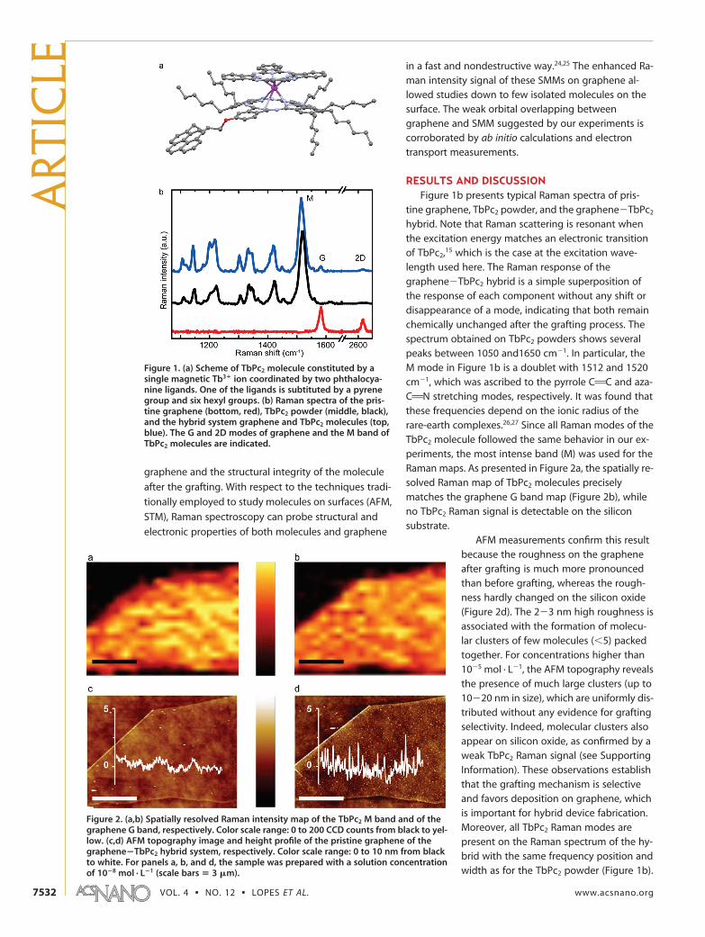
hybrid. Note that Raman scattering is resonant whenthe excitation energy matches an electronic transitionof TbPc2,15 which is the case at the excitation wave-length used here. The Raman response of thegraphene�TbPc2 hybrid is a simple superposition ofthe response of each component without any shift ordisappearance of a mode, indicating that both remainchemically unchanged after the grafting process. Thespectrum obtained on TbPc2 powders shows severalpeaks between 1050 and1650 cm�1. In particular, theM mode in Figure 1b is a doublet with 1512 and 1520cm�1, which was ascribed to the pyrrole CAC and aza-CAN stretching modes, respectively. It was found thatthese frequencies depend on the ionic radius of therare-earth complexes.26,27 Since all Raman modes of theTbPc2 molecule followed the same behavior in our ex-periments, the most intense band (M) was used for theRaman maps. As presented in Figure 2a, the spatially re-solved Raman map of TbPc2 molecules preciselymatches the graphene G band map (Figure 2b), whileno TbPc2 Raman signal is detectable on the siliconsubstrate.
AFM measurements confirm this resultbecause the roughness on the grapheneafter grafting is much more pronouncedthan before grafting, whereas the rough-ness hardly changed on the silicon oxide(Figure 2d). The 2�3 nm high roughness isassociated with the formation of molecu-lar clusters of few molecules (�5) packedtogether. For concentrations higher than10�5 mol · L�1, the AFM topography revealsthe presence of much large clusters (up to10�20 nm in size), which are uniformly dis-tributed without any evidence for graftingselectivity. Indeed, molecular clusters alsoappear on silicon oxide, as confirmed by aweak TbPc2 Raman signal (see SupportingInformation). These observations establishthat the grafting mechanism is selectiveand favors deposition on graphene, whichis important for hybrid device fabrication.Moreover, all TbPc2 Raman modes arepresent on the Raman spectrum of the hy-brid with the same frequency position andwidth as for the TbPc2 powder (Figure 1b).
Figure 1. (a) Scheme of TbPc2 molecule constituted by asingle magnetic Tb3� ion coordinated by two phthalocya-nine ligands. One of the ligands is subtituted by a pyrenegroup and six hexyl groups. (b) Raman spectra of the pris-tine graphene (bottom, red), TbPc2 powder (middle, black),and the hybrid system graphene and TbPc2 molecules (top,blue). The G and 2D modes of graphene and the M band ofTbPc2 molecules are indicated.
Figure 2. (a,b) Spatially resolved Raman intensity map of the TbPc2 M band and of thegraphene G band, respectively. Color scale range: 0 to 200 CCD counts from black to yel-low. (c,d) AFM topography image and height profile of the pristine graphene of thegraphene�TbPc2 hybrid system, respectively. Color scale range: 0 to 10 nm from blackto white. For panels a, b, and d, the sample was prepared with a solution concentrationof 10�8 mol · L�1 (scale bars � 3 �m).
ART
ICLE
VOL. 4 ▪ NO. 12 ▪ LOPES ET AL. www.acsnano.org7532

In particular, no extra peak was ob-served. The G band of graphene is onlyslightly shifted and without any broad-ening or splitting.28 These observationspoint to a weak interaction between Tb-Pc2 and graphene.
In order to get more insight, con-tact mode AFM was used to selectivelydisplace the molecules grafted ongraphene (Figure 3a). After performingcontact AFM, the graphene surface re-covered a small roughness and was freeof visible clusters, as shown in Figure3a, suggesting that the majority of allTbPc2 molecules were displaced by thetip. From the AFM profile shown in Fig-ure 3c, we estimate the volume corre-sponding to the displaced molecules;we found that the values measured ongraphene flakes are at least factor of 10larger than what we found on the SiO2
surface. Along with AFM measure-ments, we recorded Raman maps onthe same cleaned area (Figure 3b). TheTbPc2 Raman signal strongly decreasesin the cleaned area, although a weak re-sidual signal (about 15%) is still de-tected in the center of the scan (redcurve in Figure 3e), suggesting that asmall amount of molecules is left on thecleaned graphene. In particular, whileAFM measurements indicate that an im-portant quantity of molecules is presenton the edges (Figure 3b), the corre-sponding Raman signal is increasedonly by a factor of 1.4 with respect tothe decorated graphene (Figure 3d,e). We can, there-fore, conclude that the TbPc2 Raman signal does notchange linearly with the quantity of deposited mol-ecules. Additional evidence of the Raman enhance-ment is provided by Raman measurements for succes-sive deposition of different TbPc2 concentrations. Figure4a,b displays the dependence of the TbPc2 doublet Ra-man intensity on different concentrations up to 10�6
mol · L�1. The intensity follows a logarithmic behaviorwhich saturates at 10�7 mol · L�1. This nonlinear Ramanresponse is compatible with a chemical enhancementdue to a modification of the molecule polarizability, asrecently proposed by Ling et al.,29 via a charge transferwith the substrate.30�32 This effect occurs only for mol-ecules in contact with graphene,30 and therefore, onlythe first molecular monolayer is influenced, in agree-ment with the observed signal saturation for thickermolecular films. Furthermore, the graphene-inducedchemical enhancement allows the detection of theSMMs’ Raman signal for concentrations as low as 10�10
mol · L�1 (Figure 4c), while no significant roughness
change was detected on graphene by AFM. We sug-
gest that, at low concentrations, the few deposited mol-
ecules detected by the Raman signal are isolated on
the graphene surface and difficult to extract from the
AFM background signal. In conclusion, the
TbPc2�graphene interaction improves the Raman de-
tection limit, which is estimated below 100 molecules
under the laser spot of 500 nm.33 This sensitivity is re-
markable and leads us to conclude that within this level
of accuracy no particular change of the molecular struc-
tural and electronic features was observed. Despite the
described strong impact on the Raman response, the
molecule�graphene interaction seems to be weak.
In order to elucidate this experimental findings, ab
initio density functional theory calculations were per-
formed. To keep the problem tractable from the com-
putational point of view, we studied the anchoring
properties of the pyrene group alone (Figure 4e,f). Re-
cent combined scanning probe and XMCD work has
shown that unsubstituted TbPc2 molecules adsorb flat
lying on both copper33 and graphite34 surfaces with the
Figure 3. (a) Tapping AFM topography image performed after contact AFM cleaning ona 2 �m � 2 �m square to displace the TbPc2 single-molecule magnet on the graphene.Color scale range: 0 to 10 nm from black to white. (b) Raman intensity map of the TbPc2
M band for the same place as in panel a. Color scale range: 0 to 200 CCD counts fromblack to yellow. (c) Height profile of the graphene surface along the blue line repre-sented in panel a. (d) Raman intensity profile along the green curve shown in panel b.(e) Raman spectra taken at three different spots indicated by the colored circles in panelb: center (red), border (black), and outside (blue) (scale bars � 1 �m).
ARTIC
LE
www.acsnano.org VOL. 4 ▪ NO. 12 ▪ 7531–7537 ▪ 2010 7533

magnetic anisotropy axis orthogonal to the surface nor-
mal.35 Due to the chemical composition of the phthalo-
cyanine (Pc) groups in TbPc2, characterized also by
�-delocalized orbitals, it is possible to assume that Pc
and pyrene groups interact similarly with the underly-
ing substrate. In Figure 4e,f, we present a sketch of the
two systems that we have considered, namely, a pyrene
molecule adsorbed on a clean and graphene-covered
SiO2 surface (Figure 4e,f). More details on the method
and the simulated systems are given in the Supporting
Information. We find that the interaction between
pyrene and graphene (or SiO2) is noncovalent and due
to van der Waals interactions. This leads to an equilib-
rium distance of 3.2 and 2.8 Å between pyrene and
graphene or SiO2, respectively. Most importantly, our
calculations indicate that a pyrene group adsorbs more
favorably on the graphene layer than on the SiO2 sur-
face, in agreement with the experimental evidence dis-
cussed above. The binding energy of the pyrene mol-
ecule on graphene is indeed 2-fold larger than that for
the pyrene adsorbed directly on SiO2: �E(Py �
graphene � SiO2) � 1.06 eV vs �E(Py � SiO2) � 0.52 eV.
Finally, the orbital overlapping, although weak, still in-
duces changes in the electronic properties of the
graphene. In Figure 4d, we plot the G band frequency
dependence on the TbPc2 concentration. Indeed, the G
band is slightly shifted to lower frequency (4 cm�1 be-
tween extreme concentrations) as well as the 2D band
(3 cm�1 between extreme concentrations). This fre-
quency shift is compatible with a doping-induced
change of the Fermi energy.25,36 The corresponding
relative change of the Fermi energy of graphene (re-
ported on the right axis of Figure 4d) is calculated from
our Raman shift, following the work of Yan et al.25 and
Pisana et al.37 The observed logarithmic decay suggests
that the doping originates only from the molecules in
contact with graphene. Although it is strongly depend-
ent on the intrinsic doping of the pristine layer and un-
detectable for multilayer flakes, this frequency shift is
reproducible for any monolayer at the highest molecu-
lar concentration with a typical charge transfer of 1012
e/cm2. Though predicted by ab initio calculations, these
data obtained on a nonconnected graphene mono-
layer need to be confirmed by measuring the electronic
properties of a monolayer with a well-defined electri-
cal potential, as presented in the following. In order to
further probe the consequences of grafting on the elec-
tronic properties, we performed electron transport
measurements under ambient conditions on a similar
graphene flake in a FET geometry (inset of Figure 5b).
For increasing TbPc2 concentrations, the Dirac point
(corresponding to the minimum of conductance) shifts
Figure 4. (a) Evolution of the M doublet intensity according to the solution concentration. (b) Raman spectra of TbPc2 mol-ecules deposited on graphene at three different concentrations. (c) Raman intensity map of the TbPc2 deposited with a con-centration of 10�10 mol · L�1. (d) Evolution of the position of the graphene G band with TbPc2 concentration. The value forthe pristine system was 1600 cm�1. (e) Pyrene molecule anchored to clean SiO2 surface. (f) Pyrene molecule anchored tographene on SiO2 (scale bar � 3 �m).
ART
ICLE
VOL. 4 ▪ NO. 12 ▪ LOPES ET AL. www.acsnano.org7534

toward lower gate voltages, which suggests an elec-tron transfer from the TbPc2 molecules to the graphene,that is, n-doping (Figure 5a). Despite a slight asymme-try between electrons and holes induced by moleculedecoration, the graphene mobility � � �/ne (where n isthe density of carriers38 and e the electron charge) re-mains constant at 2000 cm2 · V�1 · s�1 until the con-centration reaches about 10�6 mol · L�1. This indicatesthat no significant disorder is induced in the graphene.For concentrations higher than 10�5 mol · L�1, the mo-bility drops by nearly 40% and the conductivity mini-mum broadens significantly. This is consistent with thepresence of clusters and crystallites at these high con-centrations, which induce defects and diffusion sites on
the graphene sheet and degrade progressively the mo-
bility. The relative change of the Fermi energy caused
by the TbPc2 molecules is calculated from the electrical
transport measurements and reported on Figure 5b.
The logarithmic behavior and the shift magnitude are
in good agreement with the values obtained from the
Raman frequency shift. Finally, Raman and transport ex-
periments converge on a charge transfer between
graphene and molecules of about 1012 e/cm2 that cor-
responds to 10�4 electrons per carbon atom for the
highest concentration (10�4 mol · L�1), indicating that
the electronic properties of graphene and TbPc2 are not
altered.
CONCLUSIONWe report herein evidence for a selective physisorp-
tion and homogeneous grafting of pyrene-substituted
TbPc2 single-molecule magnets onto graphene. The
decoration process is directly applicable in situ onto
graphene transistors. The enhanced Raman intensity
of TbPc2 on graphene allows the detection of molecules
down to a few tens of molecules per laser spot. Further-
more, a weak electronic interaction between graphene
and TbPc2 molecules was found. Only small charge
transfer occurs, resulting in a shift of Fermi level and
preserving graphene mobility. Our experimental find-
ings are corroborated by DFT calculations that point out
van der Waals coupling between pyrene and graphene,
leading us to conclude that TbPc2 and graphene elec-
tronic properties are essentially intact even for low mol-
ecule densities where no molecular clusters are ob-
served. Note that our main results can be applied to
other families of molecular systems with different func-
tionalities since a similar pyrene substitution can be
performed on many other compounds. Our results
show a way to probe the interactions and to provide
fabrication criteria in carbon-based molecular sensors
for spintronics applications.
EXPERIMENTAL SECTIONWe deposited graphene flakes by micromechanical exfo-
liation39 of natural graphite on degenerately doped Si witha 300 nm SiO2 capping layer. Optical microscopy and AFMwere used to determine the flake thickness and position, andthe number of layers was also confirmed by Raman spectros-copy (up to 5 layers).40 For FET devices, e-beam lithographywas performed by alignment on prelocated graphene flakes.Ten nanometer Ti/100 nm Pt contacts were deposited byelectron-gun evaporation on top of the graphene. The sili-con substrate was used as a backgate. The SMMs depositedon graphene are pyrenyl-substituted heteroleptical bis(phth-alocyaninato)terbium(III) complexes15 (Figure 1a), referredto as TbPc2 in this publication. This molecule consists of asingle magnetic Tb3� ion coordinated to two phthalocya-nine ligands (see scheme of Figure 1a). In order to improvethe grafting on graphene, one of the two phthalocyaninemacrocycles was substituted by a pyrene group and func-tionalized with six hexyl groups. Both pyrene groups and
alkyl chains are well-known to exhibit an attractive interac-tion with sp2 carbon materials, maximizing the intermolecu-lar van der Waals interactions.15,41 The molecule was depos-ited by drop casting of a TbPc2 solution in dichloromethane(DCM) with a molecule concentration ([TbPc2]) ranging from10�11 to 10�4 mol · L�1. After 5 s, the sample was rinsed inDCM and dried under nitrogen flow. Residual DCM was re-moved by a second rinse with isopropanol. The washing effi-ciency is monitored by a strong decrease of DCM fluores-cence, which is a broad band centered at 1600 cm�1. Micro-Raman spectroscopy was performed with a commercial WitecAlpha 500 spectrometer in a backscattering configuration.The excitation wavelength for all presented Raman experi-ments was the 633 nm line of a He�Ne laser with a poweraround 300 �W on the sample to prevent any damage of Tb-Pc2 and graphene. All Raman spectra were recorded with a500 nm diameter laser spot. The spectrometer was equippedwith a piezostage, which allows the measurement of Ramanintensity maps: a Raman spectrum was recorded for each
Figure 5. (a) Transfer characteristics (I, Vg) of the grapheneFET for different TbPc2 concentrations. The measurementshave been performed under ambient conditions using thelock-in technique with an AC excitation of 100 �V. Curvesare vertically shifted (by �0.3 mS) for clarity. (b) Concentra-tion dependence of the shift of the Fermi energy relative tothe pristine device. Inset: optical image and Raman intensitymap of the M doublet of the device (scale bars � 1 �m).
ARTIC
LE
www.acsnano.org VOL. 4 ▪ NO. 12 ▪ 7531–7537 ▪ 2010 7535

pixel (500 nm size), and the integrated intensity of a chosenmode was displayed with a color scale. Tapping and contactmode AFM micrographs were recorded using a VEECO D3100under ambient conditions.
Acknowledgment. This work has been supported by the ERCadvanced grant MolNanoSpin (No. 226558), EU FP7-ICT FET Open“MolSpinQIP” project, Contract N.211284, and the ANR-Pnanoproject MolNanoSpin. Computational resources have beengranted by the project “AMNOS” under the DEISA-Extreme Com-puting Initiatives. The authors thank V. Reita, E. Eyraud, L. del-Rey, D. Lepoittevin, R. Haettel, and Nanofab facility for technicalsupport.
Supporting Information Available: Additional experimental de-tails and figures. This material is available free of charge via theInternet at http://pubs.acs.org.
REFERENCES AND NOTES1. Geim, A. K.; Novoselov, K. S. The Rise of Graphene. Nat.
Mater. 2007, 6, 183–191.2. Zhang, Y.; Tan, Y.-W.; Stormer, H. L.; Kim, P. Experimental
Observation of the Quantum Hall Effect and Berry’s Phasein Graphene. Nature 2005, 438, 201–204.
3. Neto, A. C.; Guinea, F.; Peres, N.; Novoselov, K.; Geim, A.The Electronic Properties of Graphene. Rev. Mod. Phys.2009, 81, 109–162.
4. Tombros, N.; Jozsa, C.; Popinciuc, M.; Jonkman, H.; vanWees, B. Electronic Spin Transport and Spin Precession inSingle Graphene Layers at Room Temperature. Nature2007, 448, 571–574.
5. Bunch, J.; van der Zande, A.; Verbridge, S.; Frank, I.;Tanenbaum, D.; Parpia, J.; Craighead, H.; McEuen, P.Electromechanical Resonators from Graphene Sheets.Science 2007, 315, 490–493.
6. Xia, F.; Farmer, D.; ming Lin, Y.; Avouris, P. Graphene Field-Effect Transistors with High On/Off Current Ratio andLarge Transport Band Gap at Room Temperature. NanoLett. 2010, 10, 715–718.
7. Girit, C.; Bouchiat, V.; Naaman, O.; Zhang, Y.; Crommie,M. F.; Zettl, A.; Siddiqi, I. Tunable Graphene dcSuperconducting Quantum Interference Device. Nano Lett.2009, 9, 198–199.
8. Schedin, F.; Geim, A.; Morozov, S.; Hill, E.; Blake, P.;Katsnelson, M.; Novoselov, K. Detection of Individual GasMolecules Adsorbed on Graphene. Nat. Mater. 2007, 6,652–655.
9. Kessler, B.; Girit, C.; Zettl, A.; Bouchiat, V. TunableSuperconducting Phase Transition in Metal-DecoratedGraphene Sheets. Phys. Rev. Lett. 2010, 104, 047001.
10. Heersche, H.; Jarillo-Herrero, P.; Oostinga, J.; Vandersypen,L.; Morpurgo, A. Bipolar Super-Currents in Graphene.Nature 2006, 446, 56–59.
11. Elias, D.; Nair, R.; Mohiuddin, T.; Morozov, S.; Blake, P.;Halsall, M.; Ferrari, A.; Boukhvalov, D.; Katsnelson, M.; Geim,A.; et al. Control of Graphene’s Properties by ReversibleHydrogenation: Evidence for Graphane. Science 2009, 323,610–613.
12. Krasheninnikov, A.; Lehtinen, P.; Foster, A.; Pyykko, P.;Nieminen, R. Embedding Transition-Metal Atoms inGraphene: Structure, Bonding, and Magnetism. Phys. Rev.Lett. 2009, 102, 126807.
13. Dedkov, Y.; Fonin, M.; Rudiger, U.; Laubschat, C. RashbaEffect in the Graphene/Ni(111) System. Phys. Rev. Lett.2008, 100, 107602.
14. Bogani, L.; Danieli, C.; Biavardi, E.; Bendiab, N.; Barra, A.-L.;Dalcanale, E.; Wernsdorfer, W.; Cornia, A. Single-Molecule-Magnet Carbon-Nanotube Hybrids. Angew. Chem., Int. Ed.2009, 48, 746–750.
15. Klyatskaya, S.; Mascaros, J.; Bogani, L.; Hennrich, F.; Kappes,M.; Wernsdorfer, W.; Ruben, M. Anchoring of Rare-Earth-Based Single-Molecule Magnets on Single-Walled CarbonNanotubes. J. Am. Chem. Soc. 2009, 131, 15143–15151.
16. Giusti, A.; Charron, G.; Mazerat, S.; Compain, J.-D.; Mialane,P.; Dolbecq, A.; Riviere, E.; Wernsdorfer, W.; Biboum, R.;
Keita, B.; et al. Magnetic Bistability of Individual SingleMolecule Magnets Grafted on Single-Wall CarbonNanotubes. Angew. Chem., Int. Ed. 2009, 48, 4949–4952.
17. Ghirri, A.; Corradini, V.; Cervetti, C.; Candini, A.; delPennino, U.; Timco, G.; Pritchard, R.; Muryn, C.; Winpenny,R.; Affronte, M. Deposition of Functionalized Cr7NiMolecular Rings on Graphite from the Liquid Phase. Adv.Funct. Mater. 2010, 20, 1552–1560.
18. Bogani, L.; Wernsdorfer, W. Molecular Spintronics UsingSingle-Molecule Magnets. Nat. Mater. 2008, 7, 179–186.
19. Wernsdorfer, W.; Sessoli, R. Quantum Phase Interferenceand Parity Effects in Magnetic Molecular Clusters. Science1999, 284, 133–135.
20. Gatteschi, D.; Sessoli, R. Quantum Tunneling ofMagnetization and Related Phenomena in MolecularMaterials. Angew. Chem., Int. Ed. 2003, 42, 268–297.
21. Leuenberger, M. N.; Loss, D. Quantum Computing withMolecular Magnets. Nature 2001, 410, 789.
22. Affronte, M. Molecular Nanomagnets for InformationTechnologies. J. Mater. Chem. 2009, 19, 1731–1737.
23. Sanvito, S.; Rocha, A. R. Molecular-Spintronics: The Art ofDriving Spin through Molecules. J. Comput. Theor. Nanosci.2006, 3, 624–642.
24. Ferrari, A.; Meyer, J.; Scardaci, V.; Casiraghi, C.; Lazzeri, M.;Mauri, F.; Piscanec, S.; Jiang, D.; Novoselov, K.; Roth, S.; etal. Raman Spectrum of Graphene and Graphene Layers.Phys. Rev. Lett. 2006, 97, 187401.
25. Yan, J.; Zhang, Y.; Kim, P.; Pinczuk, A. Electric Field EffectTuning of Electron�Phonon Coupling in Graphene. Phys.Rev. Lett. 2007, 98, 166802.
26. Arnold, D.; Bao, M.; Biang, Y.; Jiang, J.; Ma, C.; Rintoul, L.;Wang, R. Vibrational Spectroscopy of Phthalocyanine andNaphthalocyanine in Sandwich-Type(Na)Phthalocyaninato and Porphyrinato Rare EarthComplexes. Vibr. Spectrosc. 2004, 34, 283–291.
27. Fanli Lu, J. C.; Qiuhua, Y.; Yana, X. Infrared and RamanSpectroscopic Study of Tetra-SubstitutedBis(phthalocyaninato) Rare Earth Complexes PeripherallySubstituted with tert-Butyl Derivatives. Spectrochim. Acta2006, 65, 221–228.
28. Dong, X.; Shi, Y.; Zhao, Y.; Chen, D.; Ye, J.; Yao, Y.; Gao, F.;Ni, Z.; Yu, T.; Shen, Z.; et al. Symmetry Breaking ofGraphene Monolayers by Molecular Decoration. Phys. Rev.Lett. 2009, 102, 135501.
29. Ling, X.; Xie, L.; Fang, Y.; Xu, H.; Zhang, H.; Kong, J.;Dresselhauss, M. S.; Zhang, J.; Liu, Z. Can Graphene BeUsed as a Substrate for Raman Enhancement? Nano Lett.2010, 10, 553–561.
30. Otto, A.; Mrozek, I.; Grabhorn, H.; Akemann, W. Surface-Enhanced Raman Scattering. J. Phys.: Condens. Mater.1992, 4, 1143.
31. Wright, A. R.; Cao, J. C.; Zhang, C. Enhanced OpticalConductivity of Bilayer Graphene Nanoribbons in theTerahertz Regime. Phys. Rev. Lett. 2009, 103, 207401.
32. Otto, A. The Chemical (Electronic) Contribution to Surface-Enhanced Raman Scattering. J. Raman Spectrosc. 2005, 36,497–509.
33. For a concentration C � 10�9 mol · L�1 and a volume ofdeposited drop about 1 ¡ 10 �L, with C � n/V ) n �10�15 mol, so 6.03 108 molecules. Graphene coverssilicon up to 1 ¡ 10%. So, under a laser spot of 500 nmdiameter, the number of molecules on graphene isaround 10 to 100 molecules.
34. Vitali, L.; Fabris, S.; Conte, A. M.; Brink, S.; Ruben, M.; Baroni,S.; Kern, K. Electronic Structure of Surface-SupportedBis(phthalocyaninato)terbium(III) Single MolecularMagnets. Nano Lett. 2008, 8, 3364–3368.
35. Gomez-Segura, J.; Diez-Perez, I.; Ishikawa, N.; Nakono, M.;Veciana, J.; Ruiz-Molina, D. Electronic Structure of Surface-Supported Bis(phthalocyaninato)terbium(III) SingleMolecular Magnets. Chem Commun. 2006, 27, 2866–2868.
36. Stepanow, S.; Honolka, J.; Gambardella, P.; Vitali, L.;Abdurakhmanova, N.; Tseng, T.-C.; Rauschenbach, S.; Tait,S.; Sessi, V.; Klyatskaya, S.; et al. Electronic Structure ofSurface Supported Bis(phthalocyaninato)terbium(III) Single
ART
ICLE
VOL. 4 ▪ NO. 12 ▪ LOPES ET AL. www.acsnano.org7536

Molecular Magnets. J. Am. Chem. Soc. 2010, 132,11900–11901.
37. Pisana, S.; Lazzeri, M.; Casiraghi, C.; Novoselov, K.; Geim, A.;Ferrari, A.; Mauri, F. Break-down of the AdiabaticBorn�Oppenheimer Approximation in Graphene. Nat.Mater. 2007, 6, 198–201.
38. To estimate n, we used the formula n � �(Vg� VDirac),where � � 7 1010 cm2/V is the value commonlyaccepted for a 300 nm thick SiO2 gate dielectric and wasalso confirmed by Hall measurements on similar samples.
39. Novoselov, K. S.; Geim, A. K.; Morozov, S. V.; Jiang, D.;Zhang, Y.; Dubonos, S. V.; Grigorieva, I. V.; Firsov, A. A.Electric Field Effect in Atomically Thin Carbon Films.Science 2004, 306, 666–669.
40. Malard, L.; Pimenta, M.; Dresselhaus, G.; Dresselhaus, M.Raman Spectroscopy in Graphene. Phys. Rep. 2009, 473,51–87.
41. Elemans, J.; Lei, S.; de Feyter, S. Molecular andSupramolecular Networks on Surfaces: From Two-Dimensional Crystal Engineering to Reactivity. Angew.Chem., Int. Ed. 2009, 48, 7298–7332.
ARTIC
LE
www.acsnano.org VOL. 4 ▪ NO. 12 ▪ 7531–7537 ▪ 2010 7537

![GRAFTED TOMATO - Iserv1].pdf · GRAFTED TOMATO Grafted onto ... Grafting joins the top part of one plant (the scion) to the root ... (TPIE) - January 18-20, 2012 Spring Trials in](https://img.dokumen.tips/doc/110x75/5aa1ea047f8b9a436d8c452d/grafted-tomato-1pdfgrafted-tomato-grafted-onto-grafting-joins-the-top-part.jpg)