Embed Size (px)
Citation preview

WP10 LPSC 11I
28/04/17 1/33
WP10LPSC11I_SDEU_AIT_AIV_Plan_28Apr17.docx 1 / 33
Pierre Auger Observatory
Surface Detector Electronics Upgrade
AIT- AIV Plan
Abstract:
This document defines the Assembly, Integration and Test/Verification Plan for the SDEU. It
develops the objectives, sequences and resources at system level.
Document written by: P. Stassi
Project System engineer
Agreed by: Tiina Suomijärvi
Task Leader
Date: 28 April 2017 Date: 28 April 2017
Local Reference: ATRIUM-4404 Project Reference: WP10-LPSC-11I

WP10 LPSC 11I
28/04/17 2/33
WP10LPSC11I_SDEU_AIT_AIV_Plan_28Apr17.docx 2 / 33
Table of Content 1. Introduction ........................................................................................................................................................... 5
1.1 Purpose and scope ......................................................................................................................................... 5 1.2 Documents .................................................................................................................................................... 5
1.2.1 Reference Documents ........................................................................................................................... 5 2. objectives .............................................................................................................................................................. 6 3. Models phylosophy ............................................................................................................................................... 6
3.1 Prototype Boards (PrtB) ................................................................................................................................ 6 3.2. Pre-production Boards (PpB) ........................................................................................................................ 6 3.3. Production Boards (PB) ................................................................................................................................ 6
4. Manufacturing flow charts .................................................................................................................................... 7 4.1 Prototype Boards ........................................................................................................................................... 7 4.2 Pre-production Boards .................................................................................................................................. 7 4.3 Production Boards ......................................................................................................................................... 8
5. Test Tools .............................................................................................................................................................. 9 5.1 Tank Simulator (TS) ..................................................................................................................................... 9
5.1.1 Tank Simulator Description (RD6) ....................................................................................................... 9 5.2 Basic Test Equipment (BTE) ...................................................................................................................... 12 5.3 Test PMT Equipment (TPE) ....................................................................................................................... 13 5.4 Engineering Array (EA) .............................................................................................................................. 14
6. Assembly Integration and Verification flow charts............................................................................................. 15 6.1 Prototype Boards ......................................................................................................................................... 15 6.2 Pre-production Boards ................................................................................................................................ 16 6.3 Production Boards .............................................................................................. Erreur ! Signet non défini.
7. Tests and Verification list ................................................................................................................................... 17 7.1 Mechanical verification ............................................................................................................................... 17 7.2 Thermal verification and ageing.................................................................................................................. 17 7.3 EMC ............................................................................................................................................................ 18 7.4 Electrical Functional verification ................................................................................................................ 20
7.4.1 Requirements Verification Matrix ....................................................................................................... 20 7.4.2 Basic Test definition............................................................................................................................ 24 7.4.3 Full Functional test definition ............................................................................................................. 25 7.4.4 End to End test definition .................................................................................................................... 25 7.4.5 Requirements verification by testing ................................................................................................... 27
7.5 Engineering Array verification .................................................................................................................... 30 7.5.1 Set Up Verification ............................................................................................................................. 30 7.5.2 Trigger Verification............................................................................................................................. 30 7.5.3 Timing Verification ............................................................................................................................. 30 7.5.4 Large PMTs, calibration with muons .................................................................................................. 30 7.5.5 Large PMTs, calibration with LED ..................................................................................................... 30 7.5.6 Performances comparison ................................................................................................................... 30
7.6 Models Verification Matrix ......................................................................................................................... 31 7.7 Quality Assurance ....................................................................................................................................... 31
8. ANNEX............................................................................................................................................................... 32 8.1 Detailed Basic Test procedure (TBC) ......................................................................................................... 32

WP10 LPSC 11I
28/04/17 3/33
WP10LPSC11I_SDEU_AIT_AIV_Plan_28Apr17.docx 3 / 33
ACRONYMS
AD Applicable Document
ADC Analog to Digital Converter
AIT Assembly, Integration and Tests
AIV Assembly, Integration and Verification
BGA Ball Grid Array
BTE Basic Test Equipment
CDAS Central Data Acquisition System
CPU Central Processing Unit
CR Configurational Requirement
DAC Digital to Analog Converter
DC Direct Current
DVM Digital VoltMeter
EA Engineering Array
EMC Electro-Magnetic Compatibility
ESD Electro-Static Discharge
ESS Environmental Stress Screening
ER Environmental Requirement
FADC Flash ADC
FDIR Failure Detection, Isolation and Recovery
FMECA Failure Mode, Effects and Criticality Analysis
FMEA Failure Mode, Effects Analysis
FPGA Filed Programmable Gate Array
FR Functional Requirements
GPS Global Positioning System
HASS Highly Accelerated Stress Screening
HSIA Hardware Software Interaction Analysis
HV High Voltage
H/W HardWare
ICD Interfaces Control Document
IR Interface Requirements
JTAG Joint Test Action Group
LED Light Emitting Diode
LVDS Low Voltage Differential Signaling
n/a non applicable
NCR Non Conformance Report
OR Operational Requirements
OTG On The Go
PB Production Board
PBS Product Breakdown Structure
PC Personal Computer
PCB printed Circuit Board
PMT PhotoMultiplier Tube
PpB Pre-production Board
PPS Pulse Per Second
PR Physical Requirements
PrtB Prototype Board
QR Quality Requirements
RD Reference Document
RSS Reliability Stress Screening
SDE Surface Detector Electronics
SPF Single Point Failure
SPMT Small PMT
SR Support Requirements
S/W SoftWare
TBC To Be Confirmed
TBD To Be Defined
TBW To Be Written
TC Tele-Command
TM TeleMetry
TPCB Tank Power Control Board
TS Tank Simulator
UB Unified Board
UC Upgrade Committee
USB Universal Serial Bus
UUB Upgraded Unified Board
UHE Ultra High Energy
UHECR Ultra High Energy Cosmic Ray
VM Verification Matrix
WCT Water Cerenkov Tank
WP Work Package

WP10 LPSC 11I
28/04/17 4/33
WP10LPSC11I_SDEU_AIT_AIV_Plan_28Apr17.docx 4 / 33
DOCUMENT CHANGE RECORD
Issue Revision Issue
Date
Changes
Approved by
Modified Pages Numbers, Change
Explanations and Status
11 A 23/03/14 P. Stassi DRAFT
11 B 15/05/14 P. Stassi First release
11 C 05/11/14 P. Stassi Engineering Array verifications added
11 D 28/11/14 P. Stassi Minor upgrade
11 E 01/04/15 P. Stassi Flows and test matrix update. Tests definitions
11 F 08/04/15 P. Stassi Updated with WP designers comments
11 G 15/09/15 P. Stassi M. Kleifges proposal integration, QA added.
11 H 17/10/16 P. Stassi Update before Auger prime CDR
11 I 28/04/17 P. Stassi Update for Test System internal PRR

WP10 LPSC 11I
28/04/17 5/33
WP10LPSC11I_SDEU_AIT_AIV_Plan_28Apr17.docx 5 / 33
1. INTRODUCTION
1.1 Purpose and scope
This document describes the ways and means:
- To ensure the SDEU assembly and its integration,
- To ensure its verification,
- To test and/or measure its performances.
It will:
- Present the general objectives of the SDEU AIT-AIV,
- Give the verification philosophy,
- Identify and describe the AIT-AIV tasks at system and sub-system level,
1.2 Documents
1.2.1 Reference Documents
RD1 SDEU Specifications, WP10LPSC03.
RD2 SDEU Development Plan, WP10LPSC02.
RD3 SDEU Electrical Interfaces Control Document, WP10LPSC05.
RD4 AUGER GAP NOTE, GAP-2002-002.
RD5 IEC 61004, Electromagnetic compatibility (EMC) – Part 4-2: Testing and
measurement techniques – Electrostatic discharge immunity test.
RD6 The UUB Test System, P. Buchholz and Al, Siegen University, Jan. 28th
2015
RD7 Design, Fabrication & Testing of the Auger Surface Detector Front End
Electronics Board, Daw Don Cheam, MTU – 2004.
RD8 PAO Project Management Plan – 2013-05
RD9 SDE Quality Management Plan – SDE_QMP-2002-04

WP10 LPSC 11I
28/04/17 6/33
WP10LPSC11I_SDEU_AIT_AIV_Plan_28Apr17.docx 6 / 33
2. OBJECTIVES
- Verification by means of testing of the SDEU system with respect to the specification,
including operational procedures;
- Establish an integration sequence for the units;
- Identification of test activities at unit level;
- Identify the procedures for the various tests.
3. MODELS PHYLOSOPHY
3.1 Prototype Boards (PrtB)
This model is needed to test and validate the design of the SDEU. 5 plus 20 units of
PrtB will be realized and tested at various plants. 10 units will be shipped to PAO site to
be tested on the engineering array.
3.2 Pre-production Boards (PpB)
The PpB model is needed for manufacturer qualification. 100 units are foreseen for this
purpose. Four productions sites are foreseen then the numbers of PpB will be spread
among the production sites (~ 33 units per site).
3.3 Production Boards (PB)
2000 units of the PB model will be manufactured on four production sites, equally
distributed. The PCB will be fabricated in one site only (TBC).

WP10 LPSC 11I
28/04/17 7/33
WP10LPSC11I_SDEU_AIT_AIV_Plan_28Apr17.docx 7 / 33
4. MANUFACTURING FLOW CHARTS
4.1 Prototype Boards
Figure 4.1a: Prototype boards manufacturing flow chart
4.2 Pre-production Boards
Figure 4.2a: Pre-production boards manufacturing flow chart
WP10 LPSC 11I
28/04/17 8/33
WP10LPSC11I_SDEU_AIT_AIV_Plan_28Apr17.docx 8 / 33
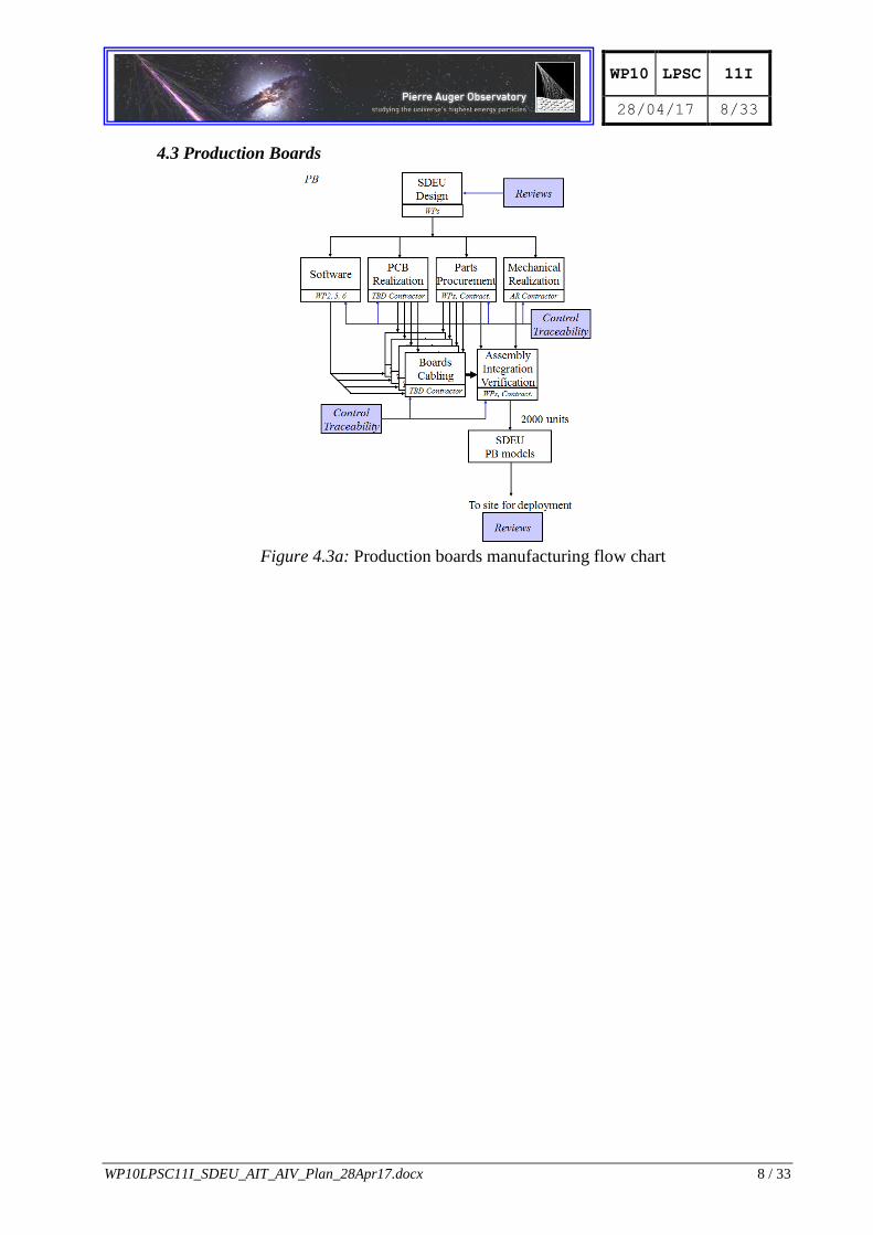
4.3 Production Boards
Figure 4.3a: Production boards manufacturing flow chart
WP10 LPSC 11I
28/04/17 9/33
WP10LPSC11I_SDEU_AIT_AIV_Plan_28Apr17.docx 9 / 33
5. TEST TOOLS
5.1 Tank Simulator or Test System (TS)
To verify all the requirements of the SDEU and also to be able to operate it at the
various test plant, a “Tank Simulator” will be built, not only able to generate or receive
and monitor signals to and from the UUB under test, but also able to have the basic
behavior of the real tank and devices around.
Additionally, this kind of simulator can be easily reproduced and spread through the
different partners, allowing sharing test and validation activities.
The “Tank Simulator” should be able to be used for the specification validation of the
UUB but also for the functional verification, fabrication and production validation and
reception, maintenance and failure detection and recovery.
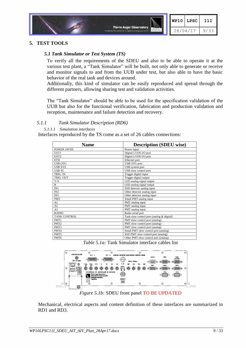
5.1.1 Tank Simulator Description (RD6)
5.1.1.1 Simulation interfaces
Interfaces reproduced by the TS come as a set of 26 cables connections:
Name Description (SDEU wise) POWER 24VDC Power input
EXT1 Digital LVDS I/O port
EXT2 Digital LVDS I/O port
ETH Ethernet port
USB OTG USB OTG port
USB SYS USB system port
USB SC USB slow control port
TRIG. IN Trigger digital input
TRIG. OUT Trigger digital output
Y/A LED analog signal output
R LED analog signal output
IN1 SSD detector analog input
IN2 Other detector analog input
IN3 Other detector analog input
PMT Small PMT analog input
A1 PMT analog input
A2 PMT analog input
A3 PMT analog input
RADIO Radio serial port
TANK CONTROL Tank slow control port (analog & digital)
PMT1 PMT slow control port (analog)
PMT2 PMT slow control port (analog)
PMT3 PMT slow control port (analog)
PMT4 Small PMT slow control port (analog)
PMT5 SSD PMT slow control port (analog)
PMT6 Other PMT slow control port (analog)
Table 5.1a: Tank Simulator interface cables list
Figure 5.1b: SDEU front panel TO BE UPDATED
Mechanical, electrical aspects and content definition of these interfaces are summarized in
RD1 and RD3.
WP10 LPSC 11I
28/04/17 10/33
WP10LPSC11I_SDEU_AIT_AIV_Plan_28Apr17.docx 10 / 33
5.1.1.2 Interaction schemes
The Tank Simulator is not intended for any mechanical test of its interfaces.
Electrical interactions parameters (load, impedance…) shall comply with SDEU
requirements (RD1, RD3) on all interfaces.
GPS antenna signal will not be considered and simulated.
5.1.1.3 On Analog interfaces
The TS will provide realistic anode PMT signals, adjustable in amplitude and time, with all
possible coincidence combination, in order to be able to test all the trigger configurations.
5.1.1.4 On power supplies interface
The TS will provide 24 Volts power supply, adjustable between 18 and 32 Volts (TBC), able
to reproduce the real voltage variation due to day and/or seasonal sun light variations.
A set of degraded interaction and fault condition schemes will be considered and
implemented (TBD).
5.1.1.5 On communication interfaces
The TS will be able to communicate on each defined port of the UUB. A set of degraded
interaction and fault condition schemes will be considered and implemented.
5.1.1.6 On Slow-Control interfaces
The TS will be able to emulate all sensors answer of the real tanks and monitor all PMT
high voltage command send by the UUB. A set of degraded interaction and fault condition
schemes will be considered and implemented.
5.1.1.7 On LED
The TS will be able to monitor the signal from the LED controller send by the UUB and
emulate PMT response on generated anode signal, accordingly to the LED signal parameters
(time, amplitude). A set of degraded interaction and fault condition schemes will be
considered and implemented.

WP10 LPSC 11I
28/04/17 11/33
WP10LPSC11I_SDEU_AIT_AIV_Plan_28Apr17.docx 11 / 33
5.1.1.8 Setup description
The local TS setup is composed with the following items:
Figure 5.1c: Tank simulator setup diagram
5.1.1.9 Application description (TBC)
The Tank Simulator applicative software allows user to:
- Generate anode PMT signals, eventually reconstructed from real signal recorded, for the 3
regular PMTs, the Small PMT and all other additional PMTs foreseen for the muon
detectors upgrade.
- Generate power supply including optionally the daily and seasonal variations recorded
from the real data.
- Generate environmental sensors signal recorded from the real data.
- Receive and monitor all slow control signal issued, used for PMT control and monitoring.
- Emulate all signal and protocol on digital I/O line, including, JTAG and trigger ports.
- Emulate the communication protocol used for the COMMS radio system.
- Emulate LED responses to signal emitted by UUB.
Additionally, the Tank Simulator should monitor and evaluate (automatically or not) all
signal incoming from the UUB under test, to perform a kind of failure detection
Moreover, the Tank simulator should be able to emulate the basic behavior of a real tank,
for example, an increase of the command voltage of the HV bias on a PMT should result
to a realistic increase of the anode pulse signal amplitude.
Additionally, to facilitate software adjustment and modification by user people, the TS
applicative software interface shall be developed in graphical programming language,
LabVIEW®.

WP10 LPSC 11I
28/04/17 12/33
WP10LPSC11I_SDEU_AIT_AIV_Plan_28Apr17.docx 12 / 33
5.2 Basic Test Equipment (BTE)
Beside the TS equipment, a Basic Test Equipment set up is defined and described below.
This equipment can be used as an alternative of the TS to perform the basic test procedure
for the production and pre-production models (TBC).
Figure 5.2a: BTE setup diagram
The Basic Test Equipment consists of:
• a power supply (30V, 2A) with current limitation and display for current and voltage
• a computer (under Linux) with test software and programmer for microcontroller and
FPGA; USB, Ethernet and JTAG cables to connect the PC with the UUB
• a fast digital oscilloscope ( < 2chn., GHz sampling)
• an active splitter (Lecce Box) to fed the signals from the LED pulser into the PMT inputs;
Alternatively a signal generator can be used.
• 6 test adapters (emulating feedback loops) for the HV monitoring outputs
• a special 26-pol flat cable to interconnect the external connectors 1/2 (for feedback loop)
Figure 5.2b: Lecce Box usage

WP10 LPSC 11I
28/04/17 13/33
WP10LPSC11I_SDEU_AIT_AIV_Plan_28Apr17.docx 13 / 33
5.3 Test PMT Equipment (TPE)
Associated with other measurement equipment, the Test PMT Equipment generates real
PMT signal toward the analog inputs of the UUB, triggered by the onboard LED controller.
The PMT polarization high voltage is provided from the UUB PMT slow control connector,
through a dedicated commercial HV module (CAEN):
Figure 5.3a: TPE setup diagram
This configuration, used to pre-prototypes and prototypes models, allows the verification
and the measurement of the analog “Front End” parameters:
- Digitalization
- Analog and digital dynamic ranges
- Linearity
- Acquisition rate
Moreover, the TPE could also being used for some trigger configuration tests and PMT slow
control algorithm.

WP10 LPSC 11I
28/04/17 14/33
WP10LPSC11I_SDEU_AIT_AIV_Plan_28Apr17.docx 14 / 33
5.4 Engineering Array (EA)
A small area, including a set of an array of 7 Water Cerenkov Tanks (WCT) equipped
with new SSD setup, dedicated for test and validation will be setup in a place of the SD
area (see map below).
These Engineering Array WCTs will be equipped with the power supply system, and
the whole communication setup. Large and small PMTs and LED flasher will be also
installed.
The EA purpose is to complete the validation of the design and to verify the
performances of the SD equipped with SDD and UUB, in situ.
Figure 5.4a: Engineering Array location
Figure 5.4b: Engineering Array Setup

WP10 LPSC 11I
28/04/17 15/33
WP10LPSC11I_SDEU_AIT_AIV_Plan_28Apr17.docx 15 / 33
6. ASSEMBLY INTEGRATION AND VERIFICATION FLOW CHARTS
6.1 Prototype Boards
Figure 6.1a: Prototype boards AIV flow chart
Legend:
Procurement
Integration, Shipment and Deployment activities
Testing and Verification activities
Testing tools
The design will be validated on the prototype boards by the WP designers and the
results of the engineering array tests on site.
ESD (EMC) test are also included in the electrical verification process, but only on the
prototype model (PrtB).

WP10 LPSC 11I
28/04/17 16/33
WP10LPSC11I_SDEU_AIT_AIV_Plan_28Apr17.docx 16 / 33
6.2 Pre-production and production Boards
Figure 6.2a: Pre-production and production boards AIV flow chart
The flow is adapted to the 4 productions sites (TBC). The S/W integrated should
include a part dedicated to test, activated with on board micro-switches.
Four sites at the minimum are foreseen for the ESS and Burning tests.
The validation of the manufacturers’ process will occur after the pre-production
deployment on site.
The production and test plan can be described in 4 steps (RD2):
- Step A, board manufacturing. Several places are foreseen, depending of
the contribution policy in the collaboration. However one unique
manufacturer (subcontractor) is recommended. Only one manufacturer for
the PCBs is foreseen.
- Step B, several place are foreseen for the commissioning, ageing and
environmental tests. These places are chosen within the institutes of the
collaboration.
- Step C, several place are foreseen for the S/W integration and full
functional tests. These places are chosen within the institutes of the
collaboration.
- On institute is responsible for the UUB shipment to the PAO site
- Step D. PAO Site, commissioning, integration, end to end tests and
deployment.

WP10 LPSC 11I
28/04/17 17/33
WP10LPSC11I_SDEU_AIT_AIV_Plan_28Apr17.docx 17 / 33
7 TESTS AND VERIFICATION LIST
7.1 Mechanical verification
The goal of SDEU mechanical verification is essentially focused of the board
dimensions, regarding the reused metallic housing and the front panel connector holes,
regarding the positions of the implemented connectors on the UUB PCB. These
verifications can be realized by review of design.
7.2 Thermal verification and ageing
Due to long operational life required, in a difficult environmental stress (daily thermal
cycling with a minimum of -15 degrees and a maximum of +55 degrees Celsius) and
also to eliminate youth default, we need an environmental stress screening and a Burn-
in procedure to enhance the reliability of each UUB.
Components are more likely to fail within the early and late life part of a device, in
consequence, the life-time reliability characteristic looks like a ‘Bath-Tub’. (RD4).
Figure 7.2a: The ‘Bath-Tub’ life-time reliability characteristic
Environmental stress screening (ESS), also known as Reliability Stress Screening
(RSS), is used in industry both at the design and the production level to minimize
failure of equipment in the field.
Design level testing is used to locate inherent faults and weaknesses within a design
before full-scale production is undertaken. Production level screening is used to locate
faulty components and manufacturing defects that would create equipment failures in
the field environment
The ESS of electronic assemblies is used to provide initial thermal ageing of devices
before delivery i.e. to accelerate the ageing of an assembly to pass through the initial
high-failure period, principally by revealing manufacturing defects.
ESS procedure is only used to provide initial ageing of devices (HASS: Highly
Accelerated Stress Screening). The objective is to detect the weakest points.
Process constraints to be used during the environmental stress screening and Burn-in, in
order to release a full HASS and to simulate usage in the field:
The UUB is powered on, and the basic functionality should be performed.
Failures appearing in hot temperature conditions are different of those appearing in cold
temperature conditions. Indeed 80% of failures (physical) occur in cold conditions
(contraction effect).
During the ESS, the power supply voltage should be chosen for the worst conditions.

WP10 LPSC 11I
28/04/17 18/33
WP10LPSC11I_SDEU_AIT_AIV_Plan_28Apr17.docx 18 / 33
Environmental conditions: humidity is between 5 to 100%, sand presence < 300 mg/m3,
salt fog is moderated.
Temperature should be reached within 30 minutes but no faster than 10 minutes to avoid
thermal shock effects.
Check of the cold/hot start capability (applying electrical stimulus: powered off during a
specified time and powered up at each extreme temperature).
We need to provide an electrical test before and after ESS and Burn-in, and a full
functional test after, using the Tank Simulator.
The feedback of the last years of electronic industry indicates that the use of Burn-in is
not as efficient as ESS (The Burn-in submits the boards to hot temperature conditions
during a specified time). Using a calibration procedure (see below) we plan to mix an
ESS with a Burn-in; First, we begin with a cold cycle, and next a Burn-in session at +70
Deg.C (16 to 40 hours, for ageing), then ESS session (10 cycles from –20 Deg.C to +70
Deg.C.; 6 Deg.C. by minute and 10 minutes extreme steps time)
Figure 7.2b: ESS and Burn-in temperature profile
7.3 EMC
EMC verification will follow the RD5 document, IEC61000, part 4-2, Testing and
measurement techniques - Electrostatic discharge (ESD) immunity test.
This standard relates to equipment, systems, subsystems and peripherals which may be
involved in static electricity discharges owing to environmental and installation
conditions, such as low relative humidity, use of low-conductivity (artificial-fiber)
carpets, vinyl garments, etc., which may exist in all locations classified in standards
relevant to electrical and electronic equipment.
Contact discharge is the preferred test method. Air discharges shall be used where
contact discharge cannot be applied. Voltages for each test method are given in Table
7.3a. The voltages shown are different for each method due to the differing methods of
test.
Table 7.3b shows the application of the test levels related to environmental (installation)
classes.
For air discharge testing, the test shall be applied at all test levels in Table 7.3a up to
and including the specified test level. For contact discharge testing, the test shall be
WP10 LPSC 11I
28/04/17 19/33
WP10LPSC11I_SDEU_AIT_AIV_Plan_28Apr17.docx 19 / 33
applied at the specified test level only unless otherwise specified by product
committees.
Table 7.3a: ESD test level
Table 7.3b: Guideline for the selection of the test levels
For the SDEU ESD tests, taking into account the PAO environment, the class 4 and
level 4 should be considered.
Figure 7.3c: Ideal contact discharge current waveform at 4 kV

WP10 LPSC 11I
28/04/17 20/33
WP10LPSC11I_SDEU_AIT_AIV_Plan_28Apr17.docx 20 / 33
7.4 Electrical Functional verification
7.4.1 Requirements Verification Matrix
The method and level for the requirements verifications are described in the
following matrix (see RD1 for a description of the requirements):
Four methods are used to verify the requirements:
- Inspection (I). The requirement implementations are verified by a visual inspection of
the system and its sub systems.
- Review of Design (R). The requirement implementations are verified by a review of
the design documents (schematics, reports, pictures, etc.) of the system and its sub
systems.
- Analysis (A). The requirement implementations are verify through analysis reports,
showing result on mathematical or software models of the sub system concerned.
- Test (T). The requirement implementations are verified through test reports showing
results on test procedures applied on the system and its sub systems.
The verifications can be performed at two levels, System (S) or Sub System (SS) or
Both (B)
Verification Matrix
Requirements Verification
ID Text Metho
d Level
FR11 The UUB shall processes analog anode signals from the three PMTs. A low and high gain signal for each
PMT shall be conditioned and digitized. T B
FR12 The total RMS integrated noise at the ADC input shall not exceed 0.5 LSB. R SS
FR13 The UUB shall digitize the PMTs anode signals at a sampling frequency of 120 Msp/s with a resolution of 12
bits minimum with the adapted conditioning and gain circuitry. R B
FR14 Adapted anti-aliasing filters shall be implemented for each PMT signal inputs (60Mhz at -3dB, TBC) (<5%
single time bin aliasing noise) T B
FR15 The UUB shall process analog signals from additional detectors R SS
FR16 The high gain/low gain ratio shall be of 32. T SS
FR17 The UUB shall processes analog anode signals from the fourth small additional PMT ( the purpose is to
increase the overall energy dynamic range). R SS
FR21 The trigger/memory circuitry shall evaluate the high-gain output of each PMT every 8.3 ns for interesting trigger patterns (see FR26), store the data in buffer and inform the micro-processor circuitry.
R S
FR22
The trigger/memory circuitry shall generate a first level trigger based upon hardware analysis of the high gain
PMT channel waveforms. The UUB micro-processor software shall imposes additional constraints to
generate a level 2 trigger signal. T B
FR23
The goal of the first level trigger shall be to trigger efficiently on UHE cosmic ray air showers of energy
>1019eV, while simultaneously rejecting lower energy showers and minimizing composition dependent trigger biases, within a rate constraint of 100 Hz.
T B
FR24 The level 1 trigger shall be designed to be flexible and eventually modifiable in the future R SS
FR25 The level 1 trigger shall start waveforms recording during 19.2 µs R SS
FR26 The triggers to be implemented are: etc.. (see RD1) R-T B
FR27 The level 1 trigger shall provide signal to Time-Tagging circuitry allowing time step of trigger and determination of absolute time of each ADC bin.
T S
FR31 The UUB shall able to time tag each events, using the information given by a commercial GPS unit and a
logic circuitry (in FPGA) based on the existing design. T B
FR32 The time tagging unit shall have a resolution of 4 ns or better, stable in temperature better than 5%. T B
FR41
The UUB shall have a micro-processor able to perform the following tasks: - Level 2 Trigger
- Data acquisition and event building with double buffering and recording
- Calibration process including analog inputs base line monitoring - Data compression to fit the communication flux limit
- Communication with the slow control management unit.
R S
FR51 The UUB shall have a slow control unit, allowing measurement and monitoring of at least 64 x 0 to 5 Volts analog input signals coded over 12 bits (can be multiplexed) and 8 logic inputs. Number of channel shall
accommodate the designs for additional muon detector. R SS

WP10 LPSC 11I
28/04/17 21/33
WP10LPSC11I_SDEU_AIT_AIV_Plan_28Apr17.docx 21 / 33
Verification Matrix
Requirements Verification
ID Text Metho
d Level
FR52 The UUB shall have a slow control unit able to generate at least 8 x 0 to 2.5 Volts analog buffered output
signals coded from 12 bits and 8 logic buffered outputs. R SS
FR53 The UUB shall have a slow control unit able to monitor internal parameters to perform a failure detection, isolation and recovery (FDIR) process on onboard power supplies and batteries voltage protection over 35 V
and under 22 V) T S
FR54 The UUB slow control unit shall be able to manage all existing SDE environmental sensors and additionally,
a water temperature sensor and an atmospheric pressure sensor. T SS
FR61
The UUB shall have a light generator unit (LED controller) able to generate two adapted signals with at least
amplitude of 20 Volts towards the two foreseen light devices (LED driver). The signal shall be controlled in
time with a resolution of 4 ns and shall be synchronized to the time tagging signal (1PPS) T S
FR62 The light devices (LED driver) shall have at least the same specifications of the existing device R SS
FR63
The light generator unit (LED controller) and light devices (LED driver) shall measure the linearity of the SD
photomultipliers (PMTs) over the full dynamic range of their acquisition channels, using the “two LEDs
technique” T S
FR64 The light generator unit (LED controller) and light devices (LED driver) shall measure the amplification ratio between overlapping acquisition channels, low and high gain of the SD PMTs
T S
FR65
The light generator unit (LED controller) and light devices (LED driver) shall be able to create artificial EAS
events of different topology on the ground SD array in order to: - check the ACQ response for different event pattern,
- check the event reconstruction
T S
FR71 The UUB shall include communication capabilities adapted to the existing unit (see Interfaces Requirements section) based on serial links
R S
FR72 The UUB shall include Ethernet communication capability. R S
FR73 The UUB shall include USB and USB OTG communication capability. R S
FR74 The UUB shall include digital communication capability for other detector systems, including
synchronization signal. T S
FR81 The UUB shall be able to produce all needed internal power supplies, regulated and stabilized, filtered and
protected, from a single input of 24 Volts nominal but varying from 18 to 30 Volts. T B
FR82 The UUB internal power supplies shall be voltage monitored by the slow control unit (FR53). R S
CR01 Each part of the UUB shall be contained in a single printed circuit board, excepted for the commercial GPS
board, light generators (LED controller shall be on UUB PCB) and the mechanical housing. I S
CR02 The SDEU shall be composed at the minimum of the following components: R S
CR11 The PMTs signal conditioning unit shall be composed of analog discrete components to perform the low
noise amplification and filtering functionalities from the actively split PMT anode signals. I B
CR21 The Digitizer unit shall be composed of a number of commercial ADC equivalents to the number of analog inputs or split inputs (dual ADC chips with LVDS outputs are recommended).
R S
CR31 The Digital Trigger unit shall be implemented in the unique FPGA component, following the architecture
described in figure 2.2.4.a below: R B
CR32 External input and output Trigger signal shall be implemented (see Interfaces Requirements). I S
CR33 Memory minimum size requirements shall follow the values described in the table 2.2.4.b of the RD1 R S
CR41 The Processing unit shall be composed of a hardcore processor in the unique FPGA component, with adapted
circuitry and memories R S
CR42 The Processing unit shall have an adapted random access memory size of 512 Mo at the minimum R S
CR43 The Processing unit shall have an adapted flash memory R S
CR44 The Processing unit shall works under a micro-Linux operating system R S
CR45 The Processing unit shall have the adapted interfaces to be able to communicate with the other UUB units and
the external world. R S
CR51 The Slow Control unit shall be composed of separate (from the main processor) micro controller, ADCs, DACs and associated circuitry on the UUB board
R B
CR52 The Slow Control unit shall have analog inputs with 10 Kilo-Ohms impedance T SS
CR53 The Slow Control unit shall include the water temperature and atmospheric pressure sensors and all existing
sensors. R S
CR54 The Slow Control unit shall have a direct USB communication link (see Interface Requirements) R S
CR61 The Calibration unit shall include a light generator unit (LED controller) implemented on the UUB PCB, able
to provide 20 Volts amplitude pulses, controlled directly by the processing unit (FPGA). T S
CR62 The Calibration unit shall include an external dual light device adapted for PMT calibration purpose (LED
driver) R S
CR71 The Time Tagging unit shall be composed of a commercial, timing dedicated, GPS board and a time tagging
algorithm implemented in the unique FPGA. R S
CR81 The UUB shall be able to manage at least 1 serial connection RS-232 type to communicate with the BSRU
(radio). R S
CR82 The UUB shall be able to manage one Ethernet connection. R S
CR83 The UUB shall be able to manage 2 USB (2.0) and one USB-OTG connection. R S
CR84 The UUB shall be able to manage 2 digital connections for other detector systems, including synchronization
signal, slow control and 24V power supply (CR93) R S

WP10 LPSC 11I
28/04/17 22/33
WP10LPSC11I_SDEU_AIT_AIV_Plan_28Apr17.docx 22 / 33
Verification Matrix
Requirements Verification
ID Text Metho
d Level
CR91
The power supplies unit shall be composed of adapted to design DC to DC converters with the following
requirements:
- Efficiency better than 80% (90% recommended) - Large input range, from 18 to 30 Volts (24V nominal)
- Low ripple noise, less than 20mV
R - T S
CR92 The 12V power supplies for PMTs bases and BSRU (radio) shall be separated (to avoid eventual failure propagation).
R S
CR93 24 Volts, filtered, non-regulated and controlled shall be provided on the extensions connectors T S
CR101
The mechanical housing shall be composed of an aluminum extruded RF proof box, identical to the existing
design (the existing box can be reused) and a metallic front panel, adapted to the new connectors type and their disposition.
I S
IR11 All the electrical interfaces between the UUB and the PMTs shall be identical to the electrical interfaces of the existing UB (excepted for the dynode connectors).
R S
IR12 All the electrical interfaces between the UUB and the Radio module shall be identical to the electrical
interfaces of the existing UB. T S
IR13 All the electrical interfaces between the UUB and GPS antenna and the tank control (from TPCB) shall be identical to the electrical interfaces of the existing UB
T S
IR14 All additional the electrical interfaces between the UUB and external world are described in the 2.3.1.a table
in the RD1. R S
IR15 The UUB shall provide external LVDS connection (EXT 1 and EXT 2) for other detector systems, including synchronization signal. The front panel connectors pin out for those extension connections, are described in
the table 2.3.1.b. of the RD1 R - T S
IR21 The UUB mechanical interfaces shall be identical to the mechanical interfaces of the existing UB. R S
IR22 The UUB mechanical front panel shall have the same external dimensions of the existing UB front panel. R S
IR23 All UUB new electrical connection toward the inner tank shall use the existing feed through (hatch cover
design document). R S
PR1 The cabled PCB of the UUB shall be within the following dimensions: I S
PR2 The complete mass of the UUB shall not exceed 10 Kg. I S
PR3 The UUB PCB shall have at least six layers minimum, with one layer for ground plane and one layer for power supplies. Class VI, minimum isolation distances 0.12mm
I S
ER1
The UUB shall be able to resist in operation to a temperature range from -20 to +70 degrees Celsius and in
storage from -40 to +80 degrees Celsius. Other parts of the SDEU (located in the tank) shall be able to resist
to a lower temperature range, -50 degrees Celsius T B
ER2 The UUB shall be able to resist in operation to an average hygrometry between 30 and 80% T S
ER3 The UUB system shall include all necessary electrical protection for internal (over current) and external
surges. T S
ER4 The UUB shall be able to resist in operation to storm lightning occurring at a distance of 1 km. T S
ER5 The UUB shall not exhibit any malfunction, degradation of performance or deviation from specified indications when test spikes are applied to the dc power input leads or electromagnetically coupled into the
equipment wiring. T S
ER6 The UUB shall resist, out of operation, to long distance cargo flight and dirty road transportation, with an adapted packaging.
T S
QR1 The UUB system shall be included in the overall Pierre Auger Observatory Quality Assurance Plan. R B
QR2 The UUB system shall follow policies and procedure described in the Pierre Auger Observatory Surface
Detector Electronics Quality Management Plan. R B
OR1 The UUB system shall be entirely autonomously powered through the existing power system. In the scope of a further extension, the total consumption shall not exceed 10W, including existing BSRU (radio, 1.1W
average, 3.6W peak) and PMT Bases (1.5W) T B
OR2 The UUB system shall be entirely controlled and monitored through the main radio communication system
(BSRU). T S
OR3 The UUB system shall be able to detect major failure and send alarm and/or initiate a recovery process with
an internal monitoring system T S
OR4 The software used in the UUB system shall be written in a standard language and widely documented to
allow modification by people not involved in the primary design phase R B
OR5 The software used in the UUB system shall be easily downloadable through the main radio communication
system and from maintenance device (computer) connected on site T B
OR6 The UUB shall be able to be in operation 24 hours over 24 hours, during 15 years. A B
SR1 The UUB system shall be designed to limit onsite maintenance at the maximum R B
SR2 Hardware and software tools and test benches shall be developed and provided to facilitate the onsite support of the UUB system
R B
SR3 Adequate quantity (15%) of spare of the major elements of the SDEU (UUB, light generators, GPS boards, I B

WP10 LPSC 11I
28/04/17 23/33
WP10LPSC11I_SDEU_AIT_AIV_Plan_28Apr17.docx 23 / 33
Verification Matrix
Requirements Verification
ID Text Metho
d Level
small PMT & bases, sensors) shall be procured and stored to facilitate onsite maintenance, in addition of the
attrition (2 to 3%) for the part procurement
SR4 The UUB system design shall allow people not involved in the design performing general maintenance operations, after a short training
I B
SR5 All support operation on the UUB system shall be completely documented, traced and recorded I B
Table 7.4a – SDEU Verification Matrix

WP10 LPSC 11I
28/04/17 24/33
WP10LPSC11I_SDEU_AIT_AIV_Plan_28Apr17.docx 24 / 33
7.4.2 Basic Test definition
The Basic Test is a verification process performed at the manufacturer plant, using a
manufacturer tool or the Basic Test Equipment and/or the Tank Simulator equipped
with reduced functionalities software (see sections 6.1, 6.2 and 6.3). The main goal
of this test is to verify the good manufacturing of the board, find faulty components,
bad soldering and the basic functions up to the connectors.
Additionally, the Basic test is a provision to verify quality assurance allowing a
feedback to the production process when performed during the earlier phase.
The table below shows the requirements which has to be tested and verified during
the Basic Test:
# Requirement to be verified Functional Requirements
FR53 The UUB shall have a slow control unit able to monitor internal parameters to perform a failure detection, isolation and recovery (FDIR) process
on onboard power supplies and batteries voltage protection over 35 V and under 22 V)
FR54 The UUB slow control unit shall be able to manage all existing SDE environmental sensors and additionally, a water temperature sensor and an
atmospheric pressure sensor.
FR81 The UUB shall be able to produce all needed internal power supplies, regulated and stabilized, filtered and protected, from a single input of 24
Volts nominal but varying from 18 to 30 Volts.
CR91
The power supplies unit shall be composed of adapted to design DC to DC converters with the following requirements:
- Efficiency better than 80% (90% recommended)
- Large input range, from 18 to 30 Volts (24V nominal)
- Low ripple noise, less than 20mV
CR93 24 Volts, filtered, non-regulated and controlled shall be provided on the extensions connectors
IR12 All the electrical interfaces between the UUB and the Radio module shall be identical to the electrical interfaces of the existing UB.
IR13 All the electrical interfaces between the UUB and GPS antenna and the tank control (from TPCB) shall be identical to the electrical interfaces of
the existing UB
ER3 The UUB system shall include all necessary electrical protection for internal (over current) and external surges.
OR1 The UUB system shall be entirely autonomously powered through the existing power system. In the scope of a further extension, the total
consumption shall not exceed 10W, including existing BSRU (radio, 1.1W average, 3.6W peak) and PMT Bases (1.5W)
The low level S/W, integrated at this level and the micro-controller S/W (Slow
Control) should contain auto test algorithm allowing too perform the following tests:
- Voltage and current measurement from the Slow Control
- Micro-controller inputs/outputs verification
- FPGA inputs/outputs verification:
o To all memories
o To communication interfaces
o To ADCs
o To LED controller
o To micro-controller
- All channel analog chain behavior, from analog connectors to the ADC inputs. This
need to provide a simple stimulus signal at the analog inputs (sinus or square
waveform)
The results of these tests can be monitored on the two Console System USB
connectors (FPGA and Micro-controller)
See in annex, the detailed Basic Test procedure.

WP10 LPSC 11I
28/04/17 25/33
WP10LPSC11I_SDEU_AIT_AIV_Plan_28Apr17.docx 25 / 33
7.4.3 Full Functional test definition
The full functional test will include all the test process listed in the section 7.4.5,
using the Tank Simulator and its complete S/W (except requirement verification
involving the GPS receiver data). The main goal is to verify all the board
functionalities in a unitary way (unit tests).
This test process shall also include:
- The Basic Tests (see 7.4.2)
- Digital connectors inputs/outputs verification (need a basic configuration in the S/W)
- LED Controller outputs verification
- PMTs slow control verification
- Communication test with GPS board (TBC)
7.4.4 End to End test definition
The End to End Test is a verification process performed on site before deployment,
using the Tank Simulator equipped with the appropriate functionalities software (see
sections 6.1, 6.2 and 6.3). The main goal is to verify all the functionality of the
system in a global way, almost in final situation, before deployment on site. The
process includes the Basic Test and additional requirement verification. See table
below:
# Requirement to be verified Functional Requirements
FR11 The UUB shall processes analog anode signals from the three PMTs. A low and high gain signal for each PMT shall be conditioned and digitized
FR16 The high gain/low gain ratio shall be of 32.
FR27 The level 1 trigger shall provide signal to Time-Tagging circuitry allowing time step of trigger and determination of absolute time of each ADC bin.
FR31 The UUB shall able to time tag each events, using the information given by a commercial GPS unit and a logic circuitry (in FPGA) based on the
existing design.
FR53 The UUB shall have a slow control unit able to monitor internal parameters to perform a failure detection, isolation and recovery (FDIR) process on
onboard power supplies and batteries voltage protection over 35 V and under 22 V)
FR54 The UUB slow control unit shall be able to manage all existing SDE environmental sensors and additionally, a water temperature sensor and an
atmospheric pressure sensor.
FR61 The UUB shall have a light generator unit (LED controller) able to generate two adapted signals with at least amplitude of 20 Volts towards the two
foreseen light devices (LED driver). The signal shall be controlled in time with a resolution of 4 ns and shall be synchronized to the time tagging
signal (1PPS)
FR63 The light generator unit (LED controller) and light devices (LED driver) shall measure the linearity of the SD photomultipliers (PMTs) over the full
dynamic range of their acquisition channels, using the “two LEDs technique”
FR64 The light generator unit (LED controller) and light devices (LED driver) shall measure the amplification ratio between overlapping acquisition
channels, low and high gain of the SD PMTs
FR65
The light generator unit (LED controller) and light devices (LED driver) shall be able to create artificial EAS events of different topology on the
ground SD array in order to:
- check the ACQ response for different event pattern,
- check the event reconstruction
FR74 The UUB shall include digital communication capability for other detector systems, including synchronization signal.
FR81 The UUB shall be able to produce all needed internal power supplies, regulated and stabilized, filtered and protected, from a single input of 24 Volts
nominal but varying from 18 to 30 Volts.
CR91
The power supplies unit shall be composed of adapted to design DC to DC converters with the following requirements:
- Efficiency better than 80% (90% recommended)
- Large input range, from 18 to 30 Volts (24V nominal)
- Low ripple noise, less than 20mV
CR93 24 Volts, filtered, non-regulated and controlled shall be provided on the extensions connectors
IR12 All the electrical interfaces between the UUB and the Radio module shall be identical to the electrical interfaces of the existing UB.
IR13 All the electrical interfaces between the UUB and GPS antenna and the tank control (from TPCB) shall be identical to the electrical interfaces of the
existing UB
IR15 The UUB shall provide external LVDS connection (EXT 1 and EXT 2) for other detector systems, including synchronization signal. The front panel
connectors pin out for those extension connections, are described in the table 2.3.1.b. of the RD1
ER6 The UUB shall resist, out of operation, to long distance cargo flight and dirty road transportation, with an adapted packaging.
OR1 The UUB system shall be entirely autonomously powered through the existing power system. In the scope of a further extension, the total
consumption shall not exceed 10W, including existing BSRU (radio, 1.1W average, 3.6W peak) and PMT Bases (1.5W)
OR2 The UUB system shall be entirely controlled and monitored through the main radio communication system (BSRU).
OR3 The UUB system shall be able to detect major failure and send alarm and/or initiate a recovery process with an internal monitoring system
OR5 The software used in the UUB system shall be easily downloadable through the main radio communication system and from maintenance device
(computer) connected on site
In this test process, one shall be able to generate a fake event on the system, using the
analog inputs (TS) and monitor the behavior of the board, reading returned data.
WP10 LPSC 11I
28/04/17 26/33
WP10LPSC11I_SDEU_AIT_AIV_Plan_28Apr17.docx 26 / 33
This need to use a system able to decode received data (a fake CDAS) which can be
connected to the Ethernet interface (the RS232 radio interface can be tested
separately with a dedicated protocol). The on board S/W should contain appropriate
routines allowing the use of the Ethernet interface.

WP10 LPSC 11I
28/04/17 27/33
WP10LPSC11I_SDEU_AIT_AIV_Plan_28Apr17.docx 27 / 33
7.4.5 Requirements verification by testing
All SDEU the requirements which can be verified by testing shall be verified and validated at system level as described in the following
verification matrix (detailed test procedure are in separate documents):
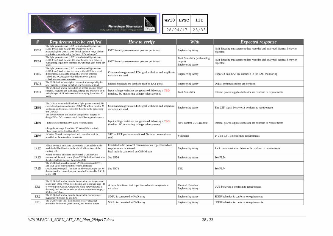
# Requirement to be verified How to verify With Expected response Functional Requirements
FR11 The UUB shall processes analog anode signals from the three
PMTs. A low and high gain signal for each PMT shall be
conditioned and digitized
Calibrated pulses send to analog input and compared to
pulse reconstructed from digital responses
Tank Simulator
Engineering Array Pulses sent en received are identical
FR14 Adapted anti-aliasing filters shall be implemented for each
PMT signal inputs (60Mhz at -3dB, TBC) (<5% single time
bin aliasing noise)
Variable frequency sine signal send to analog input and
compared to signal reconstructed from digital responses.
Tank Simulator
- no frequency scan
- only fixed frequencies
- frequencies TBD
Frequency response is within filter specification.
FR16 The high gain/low gain ratio shall be of 32. Calibrated pulses send to analog input and compared to
pulse reconstructed from digital responses Tank Simulator Gain measurement ratio is 32
FR22
The trigger/memory circuitry shall generate a first level
trigger based upon hardware analysis of the high gain PMT
channel waveforms. The UUB micro-processor software shall
imposes additional constraints to generate a level 2 trigger
signal.
Calibrated pulses send to analog input and compared to
pulse reconstructed from digital responses
Tank Simulator (no readback
of the trigger signal)
Engineering Array
Trigger signal behavior regarding the constraints is correct
FR23
The goal of the first level trigger shall be to trigger efficiently
on UHE cosmic ray air showers of energy >1019eV, while
simultaneously rejecting lower energy showers and
minimizing composition dependent trigger biases, within a
rate constraint of 100 Hz.
TBW Engineering Array TBW
FR26 The triggers to be implemented are: etc.. (see RD1) Calibrated pulses send to analog input and compared to
pulse reconstructed from digital responses Engineering Array Trigger signal behavior regarding the constraints is correct
FR27 The level 1 trigger shall provide signal to Time-Tagging
circuitry allowing time step of trigger and determination of
absolute time of each ADC bin. TBW Engineering Array TBW
FR31 The UUB shall able to time tag each events, using the
information given by a commercial GPS unit and a logic
circuitry (in FPGA) based on the existing design. Trigger signals are generated at known time interval. Engineering Array
Generated time interval is reproduced at TBD % in the taime tagging in event
files
FR32 The time tagging unit shall have a resolution of 4 ns or better,
stable in temperature better than 5%. Test to be performed at sub-system level
Thermal chamber
TBD test system
FR53
The UUB shall have a slow control unit able to monitor
internal parameters to perform a failure detection, isolation
and recovery (FDIR) process on onboard power supplies and
batteries voltage protection over 35 V and under 22 V)
Voltage variations are generated Tank Simulator (16V to 34V) Expected foreseen behavior of SC software
FR54 The UUB slow control unit shall be able to manage all
existing SDE environmental sensors and additionally, a water
temperature sensor and an atmospheric pressure sensor. Sensor stimuli is generated
Tank Simulator (for PMT
only)
Engineering Array
Expected foreseen behavior of SC software
FR61
The UUB shall have a light generator unit (LED controller)
able to generate two adapted signals with at least amplitude of
20 Volts towards the two foreseen light devices (LED driver).
The signal shall be controlled in time with a resolution of 4 ns
and shall be synchronized to the time tagging signal (1PPS)
Commands to generate LED signal with time and amplitude
variation are send. The LED signal output are monitored Engineering Array The LED signal behavior is conform to requirements
WP10 LPSC 11I
28/04/17 28/33
WP10LPSC11I_SDEU_AIT_AIV_Plan_28Apr17.docx 28 / 33
# Requirement to be verified How to verify With Expected response
FR63
The light generator unit (LED controller) and light devices
(LED driver) shall measure the linearity of the SD
photomultipliers (PMTs) over the full dynamic range of their
acquisition channels, using the “two LEDs technique”
PMT linearity measurement process performed Engineering Array PMT linearity measurement data recorded and analyzed. Normal behavior
expected
FR64
The light generator unit (LED controller) and light devices
(LED driver) shall measure the amplification ratio between
overlapping acquisition channels, low and high gain of the SD
PMTs
PMT linearity measurement process performed
Tank Simulator (with analog
output)
Engineering Array
PMT linearity measurement data recorded and analyzed. Normal behavior
expected
FR65
The light generator unit (LED controller) and light devices
(LED driver) shall be able to create artificial EAS events of
different topology on the ground SD array in order to:
- check the ACQ response for different event pattern,
- check the event reconstruction
Commands to generate LED signal with time and amplitude
variation are send. Engineering Array Expected fake EAS are observed in the PAO monitoring
FR74 The UUB shall include digital communication capability for
other detector systems, including synchronization signal. Digital messages are send and read on EXT ports Engineering Array Digital communications are conform
FR81
The UUB shall be able to produce all needed internal power
supplies, regulated and stabilized, filtered and protected, from
a single input of 24 Volts nominal but varying from 18 to 30
Volts.
Input voltage variations are generated following a TBD
timeline. SC monitoring voltage values are read Tank Simulator Internal power supplies behavior are conform to requirements
CR61
The Calibration unit shall include a light generator unit (LED
controller) implemented on the UUB PCB, able to provide 20
Volts amplitude pulses, controlled directly by the processing
unit (FPGA).
Commands to generate LED signal with time and amplitude
variation are send. Engineering Array The LED signal behavior is conform to requirements
CR91
The power supplies unit shall be composed of adapted to
design DC to DC converters with the following requirements:
- Efficiency better than 80% (90% recommended)
- Large input range, from 18 to 30 Volts (24V nominal)
- Low ripple noise, less than 20mV
Input voltage variations are generated following a TBD
timeline. SC monitoring voltage values are read Slow control UUB readout Internal power supplies behavior are conform to requirements
CR93 24 Volts, filtered, non-regulated and controlled shall be
provided on the extensions connectors
24V on EXT ports are monitored. Switch commands are
send Voltmeter 24V on EXT is conform to requirements
IR12 All the electrical interfaces between the UUB and the Radio
module shall be identical to the electrical interfaces of the
existing UB.
Emulated radio protocol communication is performed and
responses are monitored.
Real radio is connected on COMM port
Engineering Array Radio communication behavior is conform to requirements
IR13 All the electrical interfaces between the UUB and GPS
antenna and the tank control (from TPCB) shall be identical to
the electrical interfaces of the existing UB See FR54 Engineering Array See FR54
IR15
The UUB shall provide external LVDS connection (EXT 1
and EXT 2) for other detector systems, including
synchronization signal. The front panel connectors pin out for
those extension connections, are described in the table 2.3.1.b.
of the RD1
See FR74 TBD See FR74
ER1
The UUB shall be able to resist in operation to a temperature
range from -20 to +70 degrees Celsius and in storage from -40
to +80 degrees Celsius. Other parts of the SDEU (located in
the tank) shall be able to resist to a lower temperature range, -
50 degrees Celsius
A basic functional test is performed under temperature
variation
Thermal Chamber
Engineering Array UUB behavior is conform to requirements
ER2 The UUB shall be able to resist in operation to an average
hygrometry between 30 and 80% SDEU is connected to PAO array Engineering Array SDEU behavior is conform to requirements
ER3 The UUB system shall include all necessary electrical
protection for internal (over current) and external surges. SDEU is connected to PAO array Engineering Array SDEU behavior is conform to requirements

WP10 LPSC 11I
28/04/17 29/33
WP10LPSC11I_SDEU_AIT_AIV_Plan_28Apr17.docx 29 / 33
# Requirement to be verified How to verify With Expected response ER4
The UUB shall be able to resist in operation to storm lightning
occurring at a distance of 1 km. SDEU is connected to PAO array Engineering Array SDEU behavior is conform to requirements
ER5
The UUB shall not exhibit any malfunction, degradation of
performance or deviation from specified indications when test
spikes are applied to the dc power input leads or
electromagnetically coupled into the equipment wiring.
IEC61000 test procedure is applied
SDEU is connected to PAO array
SDEU behavior is conform to
requirements SDEU behavior is conform to requirements
ER6 The UUB shall resist, out of operation, to long distance cargo
flight and dirty road transportation, with an adapted
packaging. SDEU is transported and connected to PAO array Engineering Array SDEU behavior is conform to requirements
OR1
The UUB system shall be entirely autonomously powered
through the existing power system. In the scope of a further
extension, the total consumption shall not exceed 10W,
including existing BSRU (radio, 1.1W average, 3.6W peak)
and PMT Bases (1.5W)
Power is monitored Tank Simulator
Engineering Array Power values are within specifications
OR2 The UUB system shall be entirely controlled and monitored
through the main radio communication system (BSRU).
Communications under PAO protocol are emulated or
performed on COMM port Engineering Array SDEU behavior is conform to requirements
OR3 The UUB system shall be able to detect major failure and send
alarm and/or initiate a recovery process with an internal
monitoring system
Generate power modification (variation, suppression) and
monitor voltages values with the SC system Engineering Array SDEU behavior is conform to requirements and FDIR
OR5 The software used in the UUB system shall be easily
downloadable through the main radio communication system
and from maintenance device (computer) connected on site
Software download is performed through real or emulated
radio port. Checksum are monitored Engineering Array SDEU behavior is conform to requirements
Table 7.4b – SDEU Requirements testing Matrix

WP10 LPSC 11I
28/04/17 30/33
WP10LPSC11I_SDEU_AIT_AIV_Plan_28Apr17.docx 30 / 33
7.4.6 Engineering Array verification
(From Golden meeting notes, June 20, 2014)
7.4.6.1 Set Up Verification
- Set up gains of the large PMTs with rate-based method
- Set up small PMT with LED, not possible with rate method
- Noise level measurement using random triggers
7.4.6.2 Trigger Verification
- Trigger rate scans over trigger parameter space
- Compare downscale trigger to old 40 MHz trigger in triplets
- Fake event generation
- Muon decay trigger and calibration
- Rates for the new 120 MHz triggers
7.4.6.3 Timing Verification
- Check timing with twins
- Use fake events to test time jitter
7.4.6.4 Large PMTs, calibration with muons
- Muon pulse shape
- VEM calibration
- A/P calibration
- Cross calibration with small showers
- Muon decay calibration
7.4.6.5 Large PMTs, calibration with LED
- Cross-calibration of the three gain ranges
- Linearity calibration with LED
7.4.6.6 Performances comparison
- Comparison with actual electronics

WP10 LPSC 11I
28/04/17 31/33
WP10LPSC11I_SDEU_AIT_AIV_Plan_28Apr17.docx 31 / 33
7.5 Models Verification Matrix
The following matrix shows the distribution of the different verifications in function of
the models.
Verification Matrix
Feasibility
Electrical
Verification Functional Performance
Physical
Properties
Thermal &
Ageing ESD
Engineering
Array
PrtB PrtB
PpB
PB
PrtB
PpB
PB
PrtB (partly)
PpB
PB
PrtB
PpB
PB
*
PpB
PB
PrtB PrtB
Table 7.6a – Models Verification Matrix
* This process can be validated with the PrtB model
7.8 Quality Assurance
According to the SDE Quality Assurance Plan (RD9) and the Pierre Auger Observatory Quality
Assurance Plan (RD8), any test activities should be tracked in individual form sheet (physical or
electronic) and documented in test report document. Test result should be recorded in a data base
for further usage.
Any detected non conformity, founded during any test activity shall be recorded in a standard
Non Conformance Report (NCR) form sheet. The NCR procedure shall be then processed.
WP10 LPSC 11I
28/04/17 32/33
WP10LPSC11I_SDEU_AIT_AIV_Plan_28Apr17.docx 32 / 33
8 ANNEX
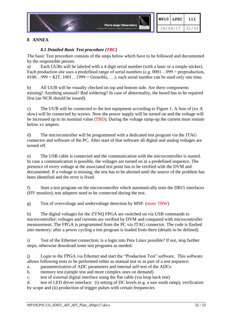
8.1 Detailed Basic Test procedure (TBC)
The basic Test procedure consists of the steps below which have to be followed and documented
by the responsible person:
a) Each UUBs will be labeled with a 4 digit serial number (with a laser or a simple sticker).
Each production site uses a predefined range of serial numbers (e.g. 0001…099 = preproduction,
0100…999 = KIT, 1001…1999 = Grenoble, …); each serial number can be used only one time.
b) All UUB will be visually checked on top and bottom side. Are there components
missing? Anything unusual? Bad soldering? In case of abnormality, the board has to be repaired
first (an NCR should be issued).
c) The UUB will be connected to the test equipment according to Figure 1. A fuse of (xx A
slow) will be connected by screws. Now the power supply will be turned on and the voltage will
be increased up to its nominal value (TBD). During the voltage ramp-up the current must remain
below xx ampere.
d) The microcontroller will be programmed with a dedicated test program via the JTAG
connector and software of the PC. After start of that software all digital and analog voltages are
turned off.
e) The USB cable is connected and the communication with the microcontroller is started.
In case a communication is possible, the voltages are turned on in a predefined sequence. The
presence of every voltage at the associated test point has to be verified with the DVM and
documented. If a voltage is missing, the test has to be aborted until the source of the problem has
been identified and the error is fixed.
f) Start a test program on the microcontroller which automatically tests the DB15 interfaces
(HV monitor); test adapters need to be connected during the test.
g) Test of overvoltage and undervoltage detection by MSP. (more TBW)
h) The digital voltages for the ZYNQ FPGA are switched on via USB commands to
microcontroller; voltages and currents are verified by DVM and compared with microcontroller
measurement. The FPGA is programmed from the PC via JTAG connector. The code is flashed
into memory; after a power cycling a test program is loaded from there (details to be defined).
i) Test of the Ethernet connection; is a login into Peta Linux possible? If not, stop further
steps; otherwise download some test programs as needed.
j) Login to the FPGA via Ethernet and start the “Production Test” software. This software
allows following tests to be performed either as manual test or as part of a test sequence:
a. parameterization of ADC parameters and internal self-test of the ADCs
b. memory test (simple test and more complex ones on demand)
c. test of external digital interface using the flat cable (via loop back test)
d. test of LED driver interface: (i) setting of DC levels (e.g. a saw tooth ramp), verification
by scope and (ii) production of trigger pulses with certain frequencies

WP10 LPSC 11I
28/04/17 33/33
WP10LPSC11I_SDEU_AIT_AIV_Plan_28Apr17.docx 33 / 33
e. use an external pulse generator or feed the LED driver pulses through the splitter to the
ADC inputs. Verify by reading out same traces that all analog channels and ADC are working
correctly.
f. readout the serial number from the GPS and start a GPS self-test to verify the
functionality of the GPS interface (TBC)
g. loop back test of the trigger-in/ trigger-out connectors
h. test of communication between FPGA and microcontroller via I2C (TBD)
i. test of reset push-button and watch-dog
j. (More TBW)
If all tests are successful, mark the board with a “green” point and fill the test sheet tracking
form; if needed load “regular” software of microcontroller and FPGA. If the test procedure was
aborted, because some tests failed, mark the boards with a red “sticker” and provide comments
on the problem on an NCR form sheet. These boards have to be kept separately for investigation
by an engineer.
End of document