Embed Size (px)
Citation preview

“Low power design of a 916MHz Gilbert Cell Mixer and a Class -A Power Amplifier for
Bioluminescent Bioreporter Integrated Circuit Transmitter”
Supriya Kilambi
Dec 2010

Abstract
This thesis presents the low power design of a 916MHz Gilbert cell mixer and a Class-A
power amplifier for the Bioluminescent Bioreporter Integrated Circuit (BBIC) transmitter.
There has been increased use in the man-made sensors which can operate in
environments unsuitable for humans and at locations remote from the observer. One such sensor
is the bioluminescent bioreporter integrated circuit (BBIC). Bioluminescent bioreporters are the
bacteria that are genetically engineered in order to achieve bioluminescence when in contact with
the target substance. The BBIC has bioreporters placed on a single CMOS integrated circuit (IC)
that detects the bioluminescence, performs the signal processing and finally transmits the senor
data. The wireless transmission allows for remote sensing by eliminating the need of costly
cabling to communicate with the sensor.
The wireless data transmission is performed by the transmitter system. The digital data
stream generated by the signal processing circuitry of the BBIC is ASK modulated for
transmission. The direct conversion transmitter used in this design includes a PLL, Mixer and a
Power amplifier. The PLL is used to generate a 916MHz frequency signal. This signal is mixed
with the digital data signal generated from the signal processing circuitry of the BBIC. A double
balanced Gilbert cell is used to perform the mixing operation. The mixer output is applied to a
power amplifier which provides amplification of the RF output power. The Gilbert cell mixer
and the power amplifier have been implemented in 90nm CMOS process available through
MOSIS.

Contents
CHAPTER 1 .................................................................................................................................................. 12
Introduction ................................................................................................................................................ 12
1.1 Biosensors ......................................................................................................................................... 12
1.2 Whole-cell Biosensors ....................................................................................................................... 12
1.3 Bioluminescent Bioreporter .............................................................................................................. 13
1.4 Bioluminescent Bioreporter Integrated Circuit ................................................................................ 14
1.5 Microluminometer System ............................................................................................................... 16
1.5.1 Photo detection ......................................................................................................................... 16
1.5.2 Signal Processing Circuitry ......................................................................................................... 19
1.6 Transmitter ....................................................................................................................................... 21
CHAPTER 2 .................................................................................................................................................. 22
Modulation Techniques .............................................................................................................................. 22
2.1 Introduction ...................................................................................................................................... 22
2.2 Modulation Techniques .................................................................................................................... 26
2.2.1 Amplitude shift keying (ASK) ...................................................................................................... 28
2.2.2 Binary- Phase shift keying (BPSK) ............................................................................................... 28
2.2.3 Frequency-Shift Keying (FSK) ..................................................................................................... 31
CHAPTER 3 .................................................................................................................................................. 33
Transmitter System ..................................................................................................................................... 33
3.1 Introduction ...................................................................................................................................... 33
3.2 Transmitter Architectures ................................................................................................................. 33
3.2.1 Super Heterodyne Transmitter .................................................................................................. 33
3.2.2 Low IF Transmitter ..................................................................................................................... 34
3.2.3 Direct conversion Transmitter ................................................................................................... 34
3.3 Mixer ................................................................................................................................................. 40
3.3.1 Gilbert Cell Mixer ....................................................................................................................... 46
3.3.2 Mixer Analysis and Design ......................................................................................................... 48
3.3.3 Mixer Bias Circuit ....................................................................................................................... 51
3.4 Power Amplifier ................................................................................................................................ 53
3.4.1 Efficiency and Gain ..................................................................................................................... 53

3.4.2 Power added efficiency .............................................................................................................. 53
3.4.3 Gain Compression ...................................................................................................................... 54
3.4.4 Total Harmonic Distortion .......................................................................................................... 54
3.5 Current Source Power Amplifiers ..................................................................................................... 56
3.5.1 Class A Power Amplifier ............................................................................................................. 56
3.5.2 Class B Power Amplifier ............................................................................................................. 57
3.5.3 Class A-B Power Amplifier .......................................................................................................... 60
3.5.4 Class C Power Amplifier ............................................................................................................. 60
3.6 Power Amplifier Design..................................................................................................................... 63
CHAPTER 4 .................................................................................................................................................. 65
Simulation and Test results ......................................................................................................................... 65
4.1 Mixer simulation results ................................................................................................................... 65
4.2 Power Amplifier simulation results ................................................................................................... 69
4.3 Entire circuit simulation results ........................................................................................................ 72
4.4 Input matching network ................................................................................................................... 76

List of Figures
Fig: 1.1 Bioluminescence chemical reaction [Eric] ...................................................................................... 15 Fig: 1.2 Conceptual BBIC system showing the immobilized bioreporters inserted between a porous layer and the integrated circuit with a photodetector [2007 IEEE] ..................................................................... 15 Fig: 1.3 Basic microluminometer system operation [Eric] .......................................................................... 18 Fig: 1.4 Available CMOS photodetectors [Eric] ........................................................................................... 18 Fig: 1.5 Block diagram of the signal processing system [Eric] ..................................................................... 20 Fig: 2.1a Baseband Signal [Razavi] .............................................................................................................. 25 Fig: 2.1b Bandpass Signal [Razavi] .............................................................................................................. 25 Fig: 2.2 Simple Communication System [Razavi] ........................................................................................ 25 Fig 2.3 Bandpass digitally modulated signals [Couch] ................................................................................ 27 Fig: 2.4 PSD of bandpass digital signal for OOK [Couch] ............................................................................. 30 Fig: 2.5 PSD of bandpass digital signal for BPSK [Couch] ............................................................................ 30 Fig: 2.6a Discontinuous-Phase FSK [Couch] ................................................................................................ 32 Fig: 2.6b Continuous-Phase FSK [Couch] .................................................................................................... 32 Fig: 3.1 Block diagram of super heterodyne 802.11a transmitter [Arya] ................................................... 36 Fig: 3.2 Block diagram of direct-conversion transmitter [Arya].................................................................. 36 Fig: 3.3a Generalized transmitter using the AM-PM generation technique [Couch] ................................. 37 Fig: 3.3b Generalized transmitter using the quadrature generation technique [Couch] ........................... 37 Fig: 3.4 Block diagram for a Transmitter system [Mo] ............................................................................... 39 Fig: 3.5 Block diagram for Phase locked loop (PLL) [Mo] ............................................................................ 39 Fig: 3.6 Linear combiner (adder) circuit and symbol [Carr] ........................................................................ 41 Fig: 3.7 Spectrum of adder output [Carr] .................................................................................................... 41 Fig: 3.8 Diode mixer circuit and symbol [Carr] ............................................................................................ 42 Fig: 3.9 Spectrum of mixer output [Carr] .................................................................................................... 42 Fig: 3.10 Typical symbol for a mixer [Jeremy] ............................................................................................. 44 Fig: 3.11 Mixing using a non-linear device [Jeremy] ................................................................................... 44 Fig: 3.12 Gilbert Mixer [YongWang] ............................................................................................................ 47 Fig: 3.13 Double balanced Gilbert Mixer [YongWang] ............................................................................... 47 Fig: 3.14 Double balanced Gilbert cell mixer .............................................................................................. 50 Fig: 3.15 Mixer bias circuit .......................................................................................................................... 51 Fig 3.16 Plot showing that the mixer bias circuit mirrors the applied off chip voltage Vdc ........................ 52 Fig 3.17 Plot showing Vgs , drain current and transconductance of RF input transistor M7 with the mixer bias voltage Vdc being swept between 0 and 1.2V. ..................................................................................... 52 Fig: 3.16 Pout vs. Pin for a generic linear amplifier [Terry] ........................................................................ 55 Fig: 3.17 Basic topology for a Current source power amplifier [Terry] ...................................................... 58 Fig: 3.18 Class-A Amplifier waveforms [Terry] ............................................................................................ 58 Fig: 3.19 Class-B Amplifier waveforms [Terry] ............................................................................................ 59 Fig: 3.20 Class-AB Amplifier waveforms [Terry] .......................................................................................... 61 Fig: 3.21 Class-C Amplifier waveforms [Terry] ............................................................................................ 62

Fig: 3.22 Power amplifier ............................................................................................................................ 64 Fig: 4.1 Test bench setup for the simulation of mixer ................................................................................ 66 Fig: 4.2 ASK modulated output obtained by performing transient analysis on the mixer ......................... 66 Fig: 4.3 Power gain of the mixer ................................................................................................................. 67 Fig: 4.4 Voltage gain of the mixer ............................................................................................................... 67 Fig: 4.5 1-dB Compression point of the mixer ............................................................................................ 68 Fig: 4.6 IP3 values of the mixer ................................................................................................................... 68 Fig: 4.7 Test bench setup for simulation of power amplifier ...................................................................... 69 Fig: 4.8 Power gain of the power amplifier ................................................................................................. 70 Fig: 4.9 Voltage gain of the power amplifier ............................................................................................... 70 Fig: 4.10 1-dB compression point of the power amplifier .......................................................................... 71 Fig: 4.11 IP3 curves of power amplifier ...................................................................................................... 71 Fig: 4.12 Test bench setup for the simulation of the entire circuit ............................................................ 73 Fig: 4.13 The amplified ASK modulated signal obtained by performing transient analysis ....................... 73 Fig: 4.14 Power gain of the entire circuit .................................................................................................... 74 Fig: 4.15 Voltage gain of the entire circuit .................................................................................................. 74 Fig: 4.16 1-dB Compression point of the entire circuit ............................................................................... 75 Fig 4.17 IP3 values of the entire circuit ....................................................................................................... 75 Fig: 4.18 S-parameters of the input matching network .............................................................................. 76

CHAPTER 1
Introduction
There is an absolute need of human sensing for human interaction in the day to day life.
We humans probably use and re-use all the five of our senses countless number of times each
and every day. However there is a need for the sensing systems which are more accurate,
versatile, and selective than a human being could ever be. This resulted in the development of
man-made sensors that can make measurements of mechanical, electrical, thermal, and chemical
quantities. These man-made sensors can operate in environments unsuitable for humans and at
locations remote from the observer.
1.1 Biosensors A sensor application in which a group of remote sensors are placed throughout an area to
be monitored is termed as distributed sensing. One class of sensors that could be helpful in
distributed sensing is biosensors. A biosensor combines a biological sensing component with an
analytical measuring element to detect, record, and transmit information regarding a
physiological change or the presence of various biological materials or chemicals in the
environment. In technical terms, a biosensor is a probe that integrates a biological component
with an electronic component to yield a measurable signal [Eric]. Biosensors are used for
monitoring changes in the environmental conditions. They come in variety of sizes and shapes
and can be used for detection and measurement of concentrations of specific bacteria or
hazardous chemicals.
1.2 Whole-cell Biosensors The biological component of the biosensor is used to recognize an analyte and
subsequently activate a signal that is being detected with a transducer. Immobilized
macromolecules such as enzymes or antibodies are used as biological components. Living
microorganisms or sections of organs or tissues are also used as biological components.
Biosensor in which an intact living cell is used as the biological component is called as whole-
cell biosensors. The whole-cell biosensors are considered to be well suited for environmental

sensing as they can be made small enough to be used in the field, and are capable of continuous
monitoring.
In recent years, there have been increased research and development efforts that have
been directed towards the development of new real-time monitoring, in-situ sensors devices that
can be easily deployed in multiple strategic locations for environmental monitoring. These
integrated sensors are small and inexpensive and are expected to be monitoring diverse physical
environments. There has also been advancement in developing various types of chemical and
biological agent sensors, such as Bioluminescent bioreporter integrated circuit (BBIC) system
developed at the University of Tennessee [ 2007 IEEE].
1.3 Bioluminescent Bioreporter Bioluminescence is the light produced by a chemical reaction in an organism. For this
chemical reaction to occur at least two chemicals are required; a substrate and luciferase. The
oxidation of the substrate is catalyzed by luciferase. The oxidation results in light and an inactive
oxidized product [Eric]. The reaction is illustrated in the Fig 1.1.
Bioreporters essentially contain two genetic elements, a promoter gene and a reporter
gene. When the target agent is present in the cell’s environment then the promoter gene is turned
on (transcribed). In normal bacteria the promoter gene is linked to the other genes that are then
likewise turned on and then translated into proteins that help the cell in either adapting or
combating to the agent that the cell has been exposed. In case of a bioreporter, these genes are
removed and replaced by reporter genes. As a result, turning on the promoter gene now causes
the reporter gene to be turned on. The promoter/reporter gene complex is transcribed into
messenger RNA (mRNA) and then translated into a reporter protein which is responsible for the
generation of a detectable signal. Therefore the generation of a signal indicates that the
bioreporter has detected a particular target agent in its environment.
Bioluminescent bioreporters are the bacteria that are genetically engineered in order to
achieve bioluminescence when in contact with the target substance. These genetically
engineered bioreporters can detect and quantify particular chemical agents in soil, air, or water
by giving off a measurable bioluminescent signal that is proportional to the concentration of the
target substance. The bioluminescent bioreporter gene emits a blue-green light (490-nm) which

can be measured rapidly. The amount of light emitted depends upon the level of expression of
the reporter gene, and thus upon the exposure level to the inducing pollutant.
1.4 Bioluminescent Bioreporter Integrated Circuit The technique used to sense bioluminescence in order to detect the presence and
concentration of a specific substance is termed as Luminometry. The typical measurement of
luminescence of a particular bioluminescent bioreporter is done using bench-top luminometers,
which use photomultiplier tubes, microchannel plates, or film as detection devices [Eric].
Though these devices are extremely sensitive they are unfortunately bound to the laboratory
because of the cost, size and fragility. Environmental sensing applications that need a large
number of distributed measurements are not well served by the present technology. Thus the
need for rugged and inexpensive luminometers that can operate in environments outside the
laboratory arises.
The concept of the bioluminescent bioreporter integrated circuit (BBIC) is
depicted in the Fig 1.2 shown below. The bioreporters are placed on a single CMOS integrated
circuit (IC) that detects the bioluminescence, executes the signal processing and transmits the
senor data. The IC can be assorted into two segments, the microluminometer which includes the
integrated photo detection and signal processing, and the transmitter which performs the wireless
data transmission. The BBIC is unique in the following two ways – first, it uses a rugged
inexpensive packaging that can be used in many remote applications outside the laboratory for
detecting the luminescence of the bioreporters ; second, it combines all the facets of the system
into one single small element. The close proximity of the bioreporters to the sensing element
wipes out the need for complex instruments to channel the light from the bioreporters to the
lumninometer. The wireless transmission allows for remote sensing by eliminating the need of
costly cabling to communicate with the sensor. The BBIC is a low power, highly sensitive and
inexpensive stand alone sensor.

Fig: 1.1 Bioluminescence chemical reaction [Eric]
Fig: 1.2 Conceptual BBIC system showing the immobilized bioreporters inserted between a
porous layer and the integrated circuit with a photodetector [2007 IEEE]

1.5 Microluminometer System The microluminometer is composed of photo detection and signal processing as shown in
the Fig 1.3. The sensor information, that is, the concentration of the targeted substance is
proportional to the intensity of light from the bioreporters. This light is converted by the
photodetector into an analog electrical signal. This analog electrical signal is converted into a
digital pulse stream by the signal processing circuitry as the light intensity must be eventually
processed digitally. Thus the microluminometer performs two signal conversions – optical to
analog current, and analog current to digital pulse stream.
1.5.1 Photo detection
1.5.1.1 Photodiode Operation
A basic p-n junction can be used to convert light into electrical current. When a photon
of sufficient energy strikes a semiconductor, the electrons in the valence band absorb the energy
of the photons and move into the conduction band if the photon energy exceeds the bandgap
energy (Eg). A typical value for Eg in silicon is 1.125eV. As a result mobile electron and
positively charged hole are created. These newly generated carriers contribute to a detectable
photocurrent if they cross the p-n junction. The depletion region of the basic p-n junction has a
built in electric field present due to the bound ions resident there. If the carriers are generated in
this depletion region then they are swept from the junction by the built in field of the depletion
region. Thus the carriers accelerate towards the contacts of the diode by the electric field. A
majority of these carriers contribute to the total generated photocurrent. Carriers generated at a
distance greater than a diffusion length from the depletion region have a less probability of
becoming a part of the total photocurrent [Eric]. These electrons generally recombine with holes
before they reach the contacts and hence they do not add up to the photocurrent. The
effectiveness of the photodetector in converting the light to a detectable electrical current is
given by its quantum efficiency.
1.5.1.2 Integrated Photo detection in CMOS
In a standard CMOS IC process three types of photodiodes are available. These
photodiodes are formed by the junctions between p-diffusion / n-well, n-diffusion / p-substrate,
and n-well / p-substrate, as shown in the Fig 1.4. The p and n diffusion regions are highly doped
and generally used as the sources/drains of transistors. The p-diffusion / n-well diode is a
reasonable choice for detecting the 490nm light generated by the bioreporters as it has a shallow
junction depth, but cannot be zero biased resulting in leakage current issues. The n-well / p-
substrate diode has a deeper junction depth though it can be zero biased for low leakage. The n-
diffusion / p-substrate diode can be zero biased and it also has a shallow junction depth, making
it a good choice for the BBIC.
A test chip incorporating the three types of photodetectors was fabricated and evaluated
in previous work [Eric]. It was observed from this work that the collection efficiencies for p-
diffusion / n-well and n-diffusion / p-substrate diodes were very poor. However, a measured
quantum efficiency of 66% at 490nm was observed for the n-well / p-substrate diode. It also
provided low leakage current of approximately 70fA for a 1V reverse bias for a bottom junction
area of 8,600 µm2 [Eric]. As a result of these tests, the n-well / p-substrate diode was chosen for
use in the BBIC. This detector has an array of small, square n-well electrodes in the p-substrate.
This method of arraying small sections decreases the junction area of the total detector which in
turn reduces the detector capacitance and leakage.

Fig: 1.3 Basic microluminometer system operation [Eric]
Fig: 1.4 Available CMOS photodetectors [Eric]
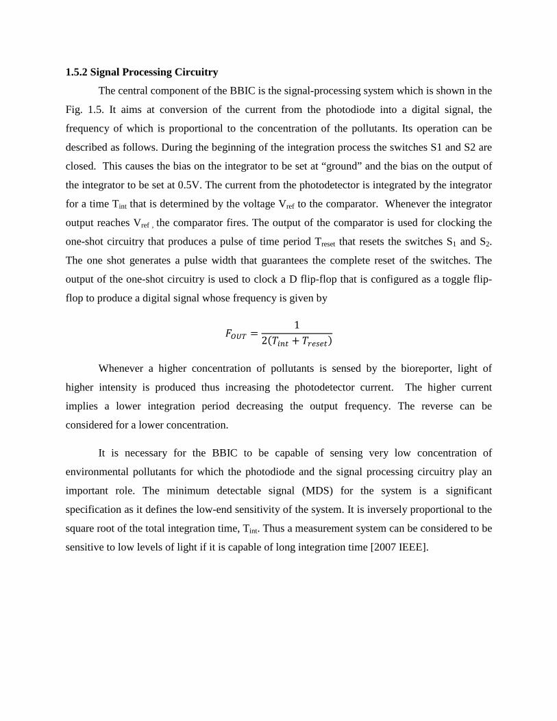
1.5.2 Signal Processing Circuitry
The central component of the BBIC is the signal-processing system which is shown in the
Fig. 1.5. It aims at conversion of the current from the photodiode into a digital signal, the
frequency of which is proportional to the concentration of the pollutants. Its operation can be
described as follows. During the beginning of the integration process the switches S1 and S2 are
closed. This causes the bias on the integrator to be set at “ground” and the bias on the output of
the integrator to be set at 0.5V. The current from the photodetector is integrated by the integrator
for a time Tint that is determined by the voltage Vref to the comparator. Whenever the integrator
output reaches Vref , the comparator fires. The output of the comparator is used for clocking the
one-shot circuitry that produces a pulse of time period Treset that resets the switches S1 and S2.
The one shot generates a pulse width that guarantees the complete reset of the switches. The
output of the one-shot circuitry is used to clock a D flip-flop that is configured as a toggle flip-
flop to produce a digital signal whose frequency is given by
𝐹𝑂𝑈𝑇 =1
2(𝑇𝑖𝑛𝑡 + 𝑇𝑟𝑒𝑠𝑒𝑡)
Whenever a higher concentration of pollutants is sensed by the bioreporter, light of
higher intensity is produced thus increasing the photodetector current. The higher current
implies a lower integration period decreasing the output frequency. The reverse can be
considered for a lower concentration.
It is necessary for the BBIC to be capable of sensing very low concentration of
environmental pollutants for which the photodiode and the signal processing circuitry play an
important role. The minimum detectable signal (MDS) for the system is a significant
specification as it defines the low-end sensitivity of the system. It is inversely proportional to the
square root of the total integration time, Tint. Thus a measurement system can be considered to be
sensitive to low levels of light if it is capable of long integration time [2007 IEEE].

Fig: 1.5 Block diagram of the signal processing system [Eric]

1.6 Transmitter The wireless data transmission is performed by this transmitter system. This integrated
wireless transmitter allows for remote sensing without the need for costly cabling to
communicate with the sensor. The digital data stream generated by the signal processing
circuitry is ASK modulated for transmission. As the BBIC is low power and requires only short
range communication this simple modulation technique has be chosen.
The direct conversion transmitter used in this design includes a PLL, Mixer and a Power
amplifier. The PLL is used to generate a 916MHz frequency signal. This signal is mixed with the
digital data signal generated from the signal processing circuitry. A doubly balanced Gilbert cell
is used to perform the mixing operation. The mixer output is applied to a power amplifier which
provides amplification of the RF output power.
This thesis describes the Gilbert cell mixer and the Power amplifier circuit designed for
the BBIC transmitter system. An insight into the various modulation techniques, transmitter
architectures and power amplifiers has been provided in the following chapters.
CHAPTER 2
Modulation Techniques
2.1 Introduction The Bioluminescent Bioreporters Integrated Circuits (BBICs) consists of the
bioluminescent bioreporters, photodiodes and signal processing circuitry. The bioreporters on
exposure to the analyte produce bioluminescence. This light is converted to into a measurable
analog electrical signal by the photodiodes. The signal processing circuitry is used to convert the
analog electrical signal into a digital pulse stream. A transmitter can be used to send this digital
data to a central node for further data collection.
In order to transmit the digital data it is necessary to modulate the incoming data onto a
carrier wave. Modulation is defined as a process that causes a shift in the range of frequencies in
a signal [Lathi.B.P]. When we talk about modulation it is necessary to define two types of
signals; baseband signal, and bandpass signal. A “baseband” signal is defined as the one whose
spectral magnitude is nonzero for the frequencies in the vicinity of ω = 0 and negligible
elsewhere [Fig. 2.1a], for example the signal generated by a microphone or a video camera. A
“bandpass” signal is a waveform whose spectral magnitude is nonzero for frequencies in a band
around a “carrier” frequency ωc and negligible outside this band [Fig. 2.1b] [Razavi] [Couch].
In general the term “baseband” is used to designate the band of frequencies of the signal
delivered by the input source. In telephony, the audio band of 0 to 3.5 kHz represents the
baseband. In television, the baseband is the video band occupying 0 to 4.3 MHz. For digital data
using signaling at a rate of Rb pulses per second the baseband is 0 to Rb Hz. In baseband
communication, the baseband signal is transmitted without any shift in the range of frequencies,
that is, without modulation. But long-haul communications over the radio link requires
modulation. By performing modulation a baseband signal is converted to its bandpass
counterpart. In other words modulation will cause the baseband signal with bandwidth B to
occupy a different bandwidth when converted to a bandpass waveform. This communication

which uses the modulation to shift the frequency spectrum of the signal is known as carrier
communication [Lathi.B.P].
The carrier wave is generally considered to be a pure sinusoidal signal, 𝑓𝑐(t). It is called
as a carrier wave as it carries the information signal from the transmitter to the receiver.
𝑓𝑐(t) = A cos (ωct + θ) (2.1)
The baseband signal (information signal or modulating signal), 𝑓(t) will be used for
varying or modulating one of the parameters of the carrier signal𝑓𝑐(t). From the Eq. 2.1 we can
find that carrier wave has three parameters that can be varied; the amplitude, A; the frequency,
ωc; and the phase, θ. Using the baseband signal to vary the amplitude, the frequency, or the
phase leads to amplitude modulation, frequency modulation, or phase modulation respectively.
The modulated signal or bandpass signal can be expressed as
𝑓𝑚(𝑡) = 𝑅𝑒 𝑔(𝑡)𝑒𝑗𝑤𝑐𝑡 (2.2a)
where Re . denotes the real part of . , 𝑔(𝑡) is called the complex envelope of 𝑓𝑚(t), and 𝑓𝑐 is
the associated carrier frequency, ωc= 2πfc. The other equivalent representations are given as
𝑓𝑚(t) = A(t) cos [ ωct + θ(t)] (2.2b)
and 𝑓𝑚(t) = 𝑥(t) cos ωct − 𝑦(t) sin ωct (2.2c)
where 𝑔(𝑡) = 𝑥(𝑡) + 𝑗𝑦(𝑡) = |𝑔(𝑡)|𝑒𝑗∠𝑔(𝑡) ≡ 𝐴(𝑡)𝑒𝑗θ(𝑡) (2.3)
𝑥(𝑡) = 𝑅𝑒𝑔(𝑡) ≡ 𝐴(𝑡) cos θ(𝑡) (2.4a)
𝑦(𝑡) = 𝐼𝑚𝑔(𝑡) ≡ 𝐴(𝑡) sin θ(𝑡) (2.4b)
𝐴(𝑡) ≜ |𝑔(𝑡)| ≡ 𝑥2(𝑡) + 𝑦2(𝑡) (2.5a)
θ(𝑡) ≜ ∠𝑔(𝑡) = tan−1 𝑦(𝑡)𝑥(𝑡)
(2.5b)
where 𝑔(𝑡), 𝑥(𝑡), 𝑦(𝑡), 𝐴(𝑡), and θ(𝑡) are all baseband waveforms [Couch].

We consider a carrier wave 𝑓𝑐(t) and vary its amplitude or phase to perform modulation.
In the Eq. 2.2b the argument ωct + θ(t) is called the “total phase” and θ(t) the “excess phase”.
The instantaneous frequency is defined as the derivative of the phase: ωc + dθ/dt is the “total
frequency” and dθ/dt is the “excess frequency” or the “frequency deviation” [Razavi].
The inverse of the modulation process is called demodulation or detection. The aim of
demodulation is to uniquely recover the information signal from the modulated carrier wave. If
we cannot reproduce the information signal f(t) accurately at the receiver then modulating it for
effective transmission is not of much use. Thus, as shown in Fig. 2.2, a simple communication
system consists of a modulator/transmitter, a channel (e.g., air or coaxial cable), and a
receiver/detector [Razavi].

Fig: 2.1a Baseband Signal [Razavi]
Fig: 2.1b Bandpass Signal [Razavi]
Fig: 2.2 Simple Communication System [Razavi]
2.2 Modulation Techniques Depending on the baseband signal, the modulation can be either analog modulation or
digital modulation. In the case of the BBIC as the data is a digital pulse stream we will consider
digital modulation techniques.
In digital “RF” systems, a digital baseband signal is used for modulating the carrier signal
using some type of generalized modulation techniques. The Power spectral density (PSD) for a
bandpass signal fm(t) is given by
𝑃𝑓𝑚(𝑓) = 14
[ 𝑃𝑔(𝑓 − 𝑓𝑐 ) + 𝑃𝑔(−𝑓 − 𝑓𝑐 )] (2.6)
where 𝑓𝑐 is the carrier frequency and 𝑃𝑔(𝑓) is the PSD of the complex envelope [Couch].
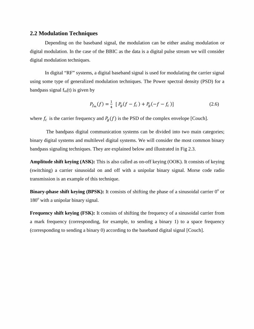
The bandpass digital communication systems can be divided into two main categories;
binary digital systems and multilevel digital systems. We will consider the most common binary
bandpass signaling techniques. They are explained below and illustrated in Fig 2.3.
Amplitude shift keying (ASK): This is also called as on-off keying (OOK). It consists of keying
(switching) a carrier sinusoidal on and off with a unipolar binary signal. Morse code radio
transmission is an example of this technique.
Binary-phase shift keying (BPSK): It consists of shifting the phase of a sinusoidal carrier 0o or
180o with a unipolar binary signal.
Frequency shift keying (FSK): It consists of shifting the frequency of a sinusoidal carrier from
a mark frequency (corresponding, for example, to sending a binary 1) to a space frequency
(corresponding to sending a binary 0) according to the baseband digital signal [Couch].
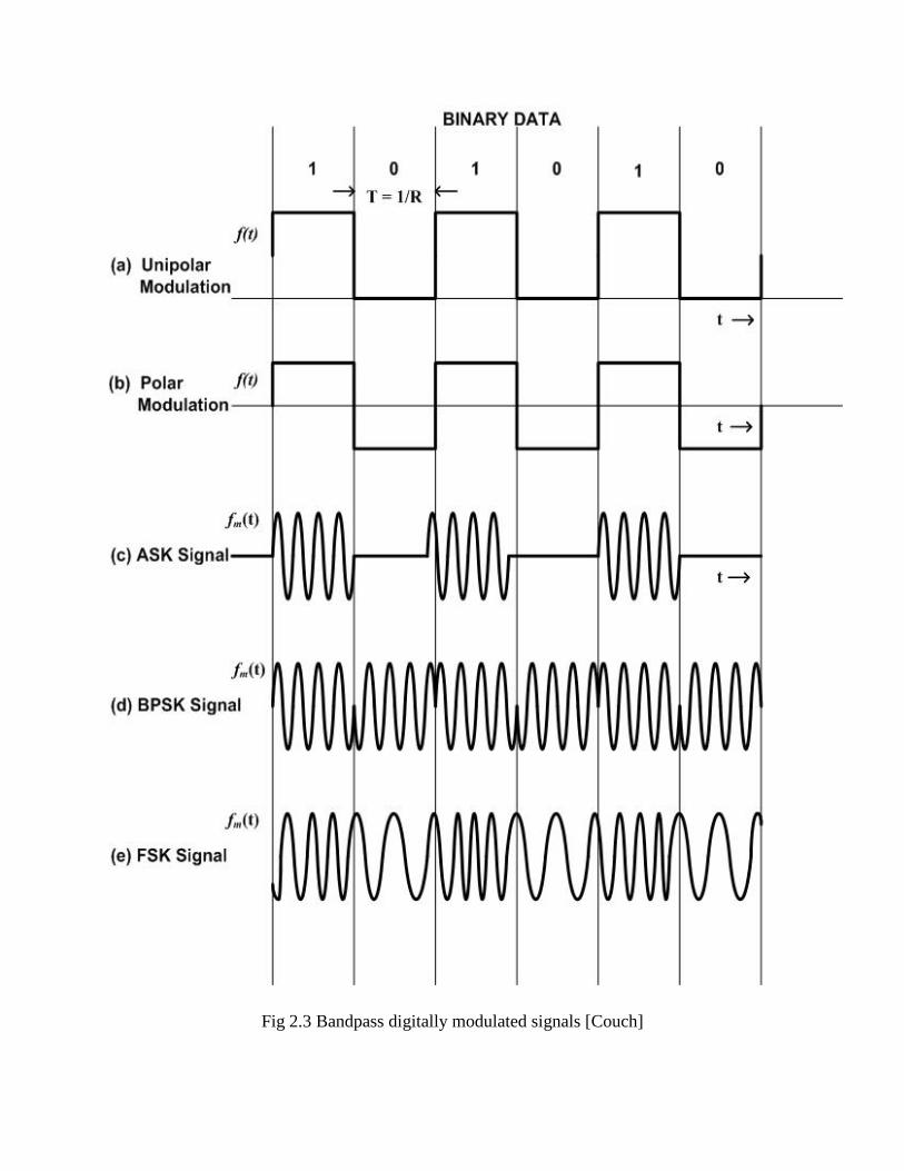
Fig 2.3 Bandpass digitally modulated signals [Couch]

2.2.1 Amplitude shift keying (ASK)
The ASK signal can be represented as shown below.
𝑓𝑚(t) = Ac 𝑓(t) cos ωct (2.7)
where 𝑓(t) is a unipolar baseband digital signal. The complex envelope for ASK is 𝑔(t) =
Ac𝑓(t) and the PSD of this complex envelope is proportional to that for the unipolar signal. It is
given by
𝑃𝑔(𝑓) = 𝐴𝑐2
2 δ(𝑓) + 𝑇𝑏
sin(𝜋𝑓𝑇𝑏)𝜋𝑓𝑇𝑏
2 for OOK (2.8)
where 𝑓(t) has a peak value of √2 so that 𝑓𝑚(t) has an average normalized power of Ac2 / 2.
The PSD for the corresponding ASK signal can be obtained by substituting Eq. 2.8 into
Eq. 2.6. The result for positive frequencies is shown in the Fig. 2.4. The bit rate is given by R =
1/ Tb. We can observe that the null-to-null bandwidth is 2R. So the transmission bandwidth of the
OOK signal can be given as BT= 2B where B is the baseband bandwidth [Couch].
2.2.2 Binary- Phase shift keying (BPSK)
The BPSK signal is represented as shown below.
𝑓𝑚(t) = Ac cos ωct + 𝐷𝑝𝑓(t) (2.9)
where 𝑓(t) is a polar based baseband digital signal with peak values of ±1. By expanding Eq.
2.9 we get
𝑓𝑚(t) = Ac cos Dp𝑓(t) cosωct − Ac sin Dp𝑓(t) sinωct (2.10)
Considering that cos(𝑥) and sin (𝑥) are even and odd functions of x, and 𝑓(t) has values
of ±1 the above Eq. 2.10 can be reduced to
𝑓𝑚(t) = Ac cosDp cosωct − Ac sinDp𝑓(t) sinωct (2.11)
The first term in the Eq.2.11 is called the pilot carrier term and the second term is called
the data term. The level of the pilot carrier term is set by the value of Dp (the peak deviation∆θ =
𝐷𝑝). If Dp is small then the amplitude of the pilot carrier term is relatively large compared to the
data term. Thus there will be very little power in the data term which contains the source
information. To maximize the signaling efficiency the power in the data term needs to be
maximized. This can be achieved by setting∆θ = 90°. Then the BPSK signal becomes
𝑓𝑚(t) = Ac 𝑓(t) sinωct (2.12)
The complex envelope for this signal is 𝑔(t) = 𝑗Ac𝑓(t) and the PSD for the complex
envelope is
𝑃𝑔(𝑓) = 𝐴𝑐2 𝑇𝑏 sin(𝜋𝑓𝑇𝑏)𝜋𝑓𝑇𝑏
2 (2.13)
𝑓𝑚(t) has an average normalized power of Ac2 / 2. The PSD for the BPSK signal can be
found by substituting Eq.2.13 into Eq.2.6. The result spectrum is shown in Fig 2.5. The null-to-
null bandwidth is 2R [Couch].

Fig: 2.4 PSD of bandpass digital signal for OOK [Couch]
Fig: 2.5 PSD of bandpass digital signal for BPSK [Couch]
2.2.3 Frequency-Shift Keying (FSK)
FSK signal can be generated by switching the transmitter output line between two
different oscillators as shown in the Fig. 2.6a. As this generates an output waveform that is
discontinuous at the switching times it is called discontinuous-phase FSK. This can be
represented by
𝑓𝑚(𝑡) = 𝐴𝑐 cos(ω1𝑡 + θ1) , for 𝑡 in the time interval when a binary 1 is sent𝐴𝑐 cos(ω2𝑡 + θ2) , for 𝑡 in the time interval when a binary 0 is sent
(2.14)
where f1 is called the mark (binary 1) frequency and f2 is called the space (binary 0) frequency.
The continuous-phase FSK signal can be generated by feeding the data signal into a
frequency modulator, as shown in the Fig. 2.6b. The resultant signal can be represented by
𝑓𝑚(𝑡) = 𝐴𝑐 𝑐𝑜𝑠 ω𝑐𝑡 + 𝐷𝑓 ∫ 𝑓(𝜆) 𝑑𝜆𝑡−∞ (2.15a)
or 𝑓𝑚(𝑡) = 𝑅𝑒𝑔(𝑡)𝑒𝑗ω𝑐𝑡 (2.15b)
where 𝑔(𝑡) = 𝐴𝑐𝑒𝑗θ(𝑡) (2.15c)
θ(𝑡) = 𝐷𝑓 ∫ 𝑓(𝜆) 𝑑𝜆𝑡−∞ (2.15d)
The spectra of the FSK signals are difficult to evaluate since the complex envelope, 𝑔(𝑡),
is a nonlinear function of 𝑓(t)[Couch].

Fig: 2.6a Discontinuous-Phase FSK [Couch]
Fig: 2.6b Continuous-Phase FSK [Couch]
CHAPTER 3
Transmitter System
3.1 Introduction This chapter initially discusses the various types of transmitter architectures. Then it will
examine in detail the Gilbert cell mixer. The various types of Power amplifiers are explained
followed by the discussion of the power amplifier design.
3.2 Transmitter Architectures In general, three types of common transmitter architectures are available; super
heterodyne, low IF, and direct conversion. Each of these architectures has its own inherent
strengths and weaknesses. We will investigate the architectures in the following section.
3.2.1 Super Heterodyne Transmitter
The super heterodyne architecture is sketched in the Fig 3.1. The digital baseband signals
are passed through the DACs to generate the appropriate I and Q analog baseband signals. These
signals are then passed through low pass filters to reject any high frequency aliasing caused by
the DACs. In the example considered here the filtered I and Q signals are passed on to
quadrature up-converting mixers running with LO signals at 1.28GHz. They are combined and a
single side-band modulated signal is generated at IF (1.28 GHz). The signal is then passed
through a band pass filter in order to reduce spurious signals and to reject any residual DAC
aliasing that may have not been completely rejected by the digital and analog baseband filters.
The filtered IF signal is then passed through a RF mixer to generate the RF signal at 4.9 to 5.805
GHz depending on the LO frequency. Before passing the signal through a power amplifier,
depending on the application another stage of filtering may be applied. The multiple up
conversions result in the use of multiple filters in this architecture. Every time a mixing action
takes place one needs to be aware of any image components that may be created.
The super heterodyne transmitter has a good performance, can achieve very good
quadrature balance, can reject extraneous spurs due to extended filtering, and is reasonably low
power. On the other hand, this architecture is comparatively large and expensive, has many
discrete components and is not suitable for multimode applications due to the narrow band nature
of the IF filter [Arya].
3.2.2 Low IF Transmitter
The low IF transmitter works similar to a direct conversion transmitter but it requires full
image reject mixers. It has a complex architecture and is seldom used for WLAN applications.
This architecture is more popular for narrowband signals. When the low IF architecture is being
used, the first stage of up conversion is to be performed on digital domain so that high degree of
image rejection can be maintained.
3.2.3 Direct conversion Transmitter
An example for this architecture is shown in the Fig 3.2. The baseband signals I and Q
are passed through DACs and then through low pass filters to reject any high frequency aliasing
caused by the DACs. The filtered signals are then applied to quadrature up-converting mixers.
Then the resultant signals are combined and applied to a power amplifier.
This architecture eliminates the IF bandpass filter and the requirements for image
filtering and thus offers the lowest overall cost. This architecture provides the highest degree of
integration. It can be made to offer high performance and low power consumption. These
advantages resulted in choosing this architecture for the BBIC transmitter.
Transmitters generate the modulated signal from the modulating signal 𝑓(t) at the carrier
frequency fc. As already mentioned in the previous section the modulated signal can be
represented by Eq. 2.2a, Eq.2.2b, Eq. 2.2c
𝑓𝑚(𝑡) = 𝑅𝑒 𝑔(𝑡)𝑒𝑗𝑤𝑐𝑡

or, 𝑓𝑚(t) = A(t) cos [ ωct + θ(t)]
and 𝑓𝑚(t) = 𝑥(t) cos ωct − 𝑦(t) sin ωct
The above two equations can be used to represent the following generalized transmitters
using the direct conversion architecture. The Eq. 2.2b represents a generalized transmitter using
the AM-PM generation technique as shown in the Fig. 3.3a. A(t) and θ(t) are generated from
𝑓(t) by the baseband signal processing circuit. Nonlinear analog circuits or a digital computer
incorporating the A and θ algorithms can be used to implement the signal processing. ADC and
DAC are needed in the implementation using a digital computer. As indicated in the Fig. 3.3a the
remainder of the AM-PM canonical form requires RF circuits.
Fig. 3.3b represents the generalized transmitter using the quadrature generation
technique. In-phase and quadrature-phase processing is used in this technique. By using analog
hardware or digital hardware with software the baseband signal processing may be implemented.
As indicated in the Fig 3.3b the remainder of the canonical form requires RF circuits [Couch].

Fig: 3.1 Block diagram of super heterodyne 802.11a transmitter [Arya]
Fig: 3.2 Block diagram of direct-conversion transmitter [Arya]
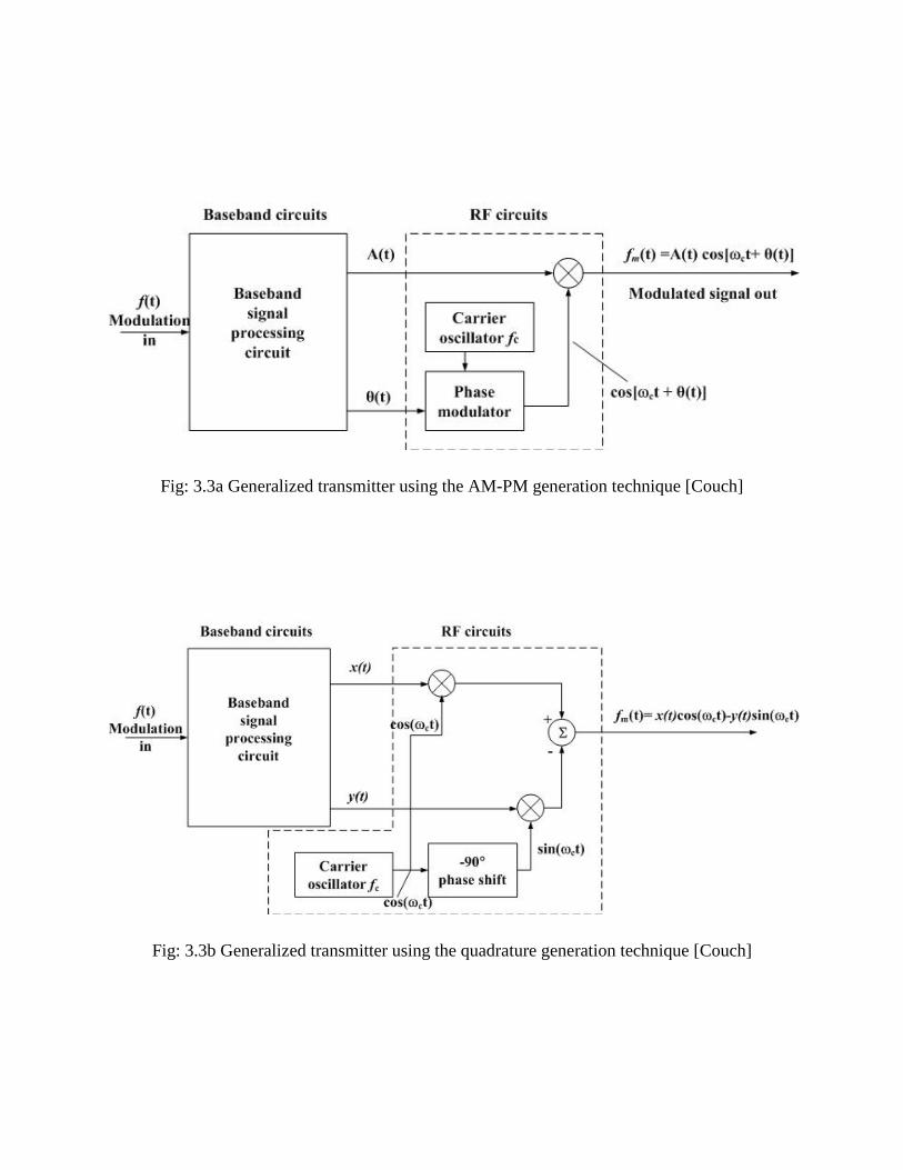
Fig: 3.3a Generalized transmitter using the AM-PM generation technique [Couch]
Fig: 3.3b Generalized transmitter using the quadrature generation technique [Couch]

We know that the amplitude shift keying is the simplest modulation technique used in
data communications. It is not a good choice for long transmission distances as it is not robust
enough to prevent the effect of noise during data transmission over long distances. As BBIC
requires only short range communication this simple modulation technique has be chosen. Then
the AM-PM generation technique showed in the Fig 3.3a can be replaced by a more simpler and
general transmitter structure as shown in the Fig 3.4.
This structure of direct conversion transmitter is made up of Phase locked loop (PLL),
Mixer, Power amplifier and Antenna. In the Fig 3.4 the Data represents the signal coming out of
the signal processing circuitry of the BBIC. This signal is mixed with the 916MHz signal
generated by the PLL.
The block diagram of the PLL is shown in the Fig 3.5. It includes a crystal frequency
reference, a phase / frequency detector, a loop filter, a voltage controlled oscillator and a
frequency divider (divided by 256). The phase / frequency detector is used for comparing the
phase / frequency difference between the clock signal coming out of the frequency divider and
the frequency reference. Then the charge pump will generate a control voltage for the VCO
according to the phase / frequency difference. The loop filter is used to remove the high
frequency components of the control voltage and provide a relatively stable one to adjust the
frequency of the VCO. The signal frequency from the VCO is divided by 256 by the frequency
divider. The PLL has a feedback loop and this makes the output frequency of the VCO stable
[Mo]. This stable frequency is important for the RF transmission and is the input to the mixer.
The mixer is an important component of the transmitter and is of primary interest for us. It is
used for multiplying the Data signal coming out of the signal processing circuitry of the BBIC
with the 916MHz frequency signal generated by the PLL. [Mo]

Fig: 3.4 Block diagram for a Transmitter system [Mo]
Fig: 3.5 Block diagram for Phase locked loop (PLL) [Mo]
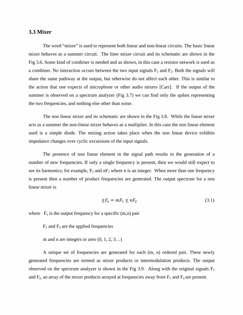
3.3 Mixer
The word “mixer” is used to represent both linear and non-linear circuits. The basic linear
mixer behaves as a summer circuit. The liner mixer circuit and its schematic are shown in the
Fig 3.6. Some kind of combiner is needed and as shown, in this case a resistor network is used as
a combiner. No interaction occurs between the two input signals F1 and F2. Both the signals will
share the same pathway at the output, but otherwise do not affect each other. This is similar to
the action that one expects of microphone or other audio mixers [Carr]. If the output of the
summer is observed on a spectrum analyzer (Fig 3.7) we can find only the spikes representing
the two frequencies, and nothing else other than noise.
The non linear mixer and its schematic are shown in the Fig 3.8. While the linear mixer
acts as a summer the non-linear mixer behaves as a multiplier. In this case the non linear element
used is a simple diode. The mixing action takes place when the non linear device exhibits
impedance changes over cyclic excursions of the input signals.
The presence of non linear element in the signal path results in the generation of a
number of new frequencies. If only a single frequency is present, then we would still expect to
see its harmonics; for example, F1 and nF1 where n is an integer. When more than one frequency
is present then a number of product frequencies are generated. The output spectrum for a non
linear mixer is
±𝐹𝑜 = 𝑚𝐹1 ± 𝑛𝐹2 (3.1)
where Fo is the output frequency for a specific (m,n) pair
F1 and F2 are the applied frequencies
m and n are integers or zero (0, 1, 2, 3…)
A unique set of frequencies are generated for each (m, n) ordered pair. These newly
generated frequencies are termed as mixer products or intermodulation products. The output
observed on the spectrum analyzer is shown in the Fig 3.9. Along with the original signals F1
and F2, an array of the mixer products arrayed at frequencies away from F1 and F2 are present.
Fig: 3.6 Linear combiner (adder) circuit and symbol [Carr]
Fig: 3.7 Spectrum of adder output [Carr]
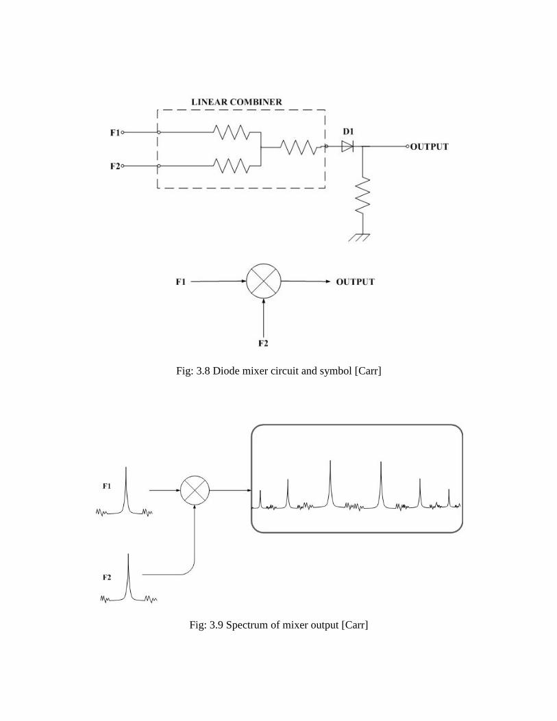
Fig: 3.8 Diode mixer circuit and symbol [Carr]
Fig: 3.9 Spectrum of mixer output [Carr]

From the Eq 3.1 it can be implied that a number of frequency products are generated of
which not all are useful for any specific purpose. Then why do we need to use a mixer? The main
purpose of using a mixer is to translate the frequency and in the process transfer the modulation
of the original signal. For example, when an AM signal is received, and then translated to a
different frequency in the receiver, the modulation characteristics should be essentially
undistorted for the AM signal at the new frequency.
Thus a mixer is used for translating the signal spectrum from one frequency to another.
In other words a mixer is needed to perform frequency translation. The typical symbol of the
mixer is shown in the Fig 3.10.
Ideally a mixer should multiply the RF and LO signals to produce the IF signal. It should
therefore translate the input spectrum from one frequency to another without any distortion and
degradation in noise performance. Most of these requirements can be met by considering the
perfect multiplication of two signals as illustrated in the Eq 3.2 below.
(𝑉1 cos ω1𝑡)(𝑉2 cos ω2𝑡) = 𝑉1𝑉22
(cos(ω1 + ω2)𝑡 + cos(ω1 − ω2)𝑡) (3.2)
From the above equation it can be observed that the output which is the product of the
two input frequencies consists of the sum and difference frequencies. No other frequency terms
than these two are generated and any unwanted signals can be easily removed by filtering.
This mixing is generally achieved by applying the two signals to a non linear device as
mentioned already in the above discussion and as shown in the Fig 3.11. The non linearity can
be expressed in the form of Taylor series as in the Eq 3.3 [Jeremy].
𝐼𝑜𝑢𝑡 = 𝐼0 + 𝑎[𝑉𝑖(𝑡)] + 𝑏[𝑉𝑖(𝑡)]2 + 𝑐[𝑉𝑖(𝑡)]3 + ⋯ (3.3)
where 𝑉𝑖 = 𝑉1 + 𝑉2

Fig: 3.10 Typical symbol for a mixer [Jeremy]
Fig: 3.11 Mixing using a non-linear device [Jeremy]

Considering the squared term
𝑏(𝑉1 + 𝑉2)2 = 𝑏(𝑉12 + 2𝑉1𝑉2 + 𝑉22) (3.4)
It can immediately be observed that the squared term includes a product term and
therefore this can be used for the mixing process.
One of the approaches for classifying mixers is whether or not they are unbalanced,
single balanced or double balanced.
Unbalanced mixers:
Both RF and LO signals appear in the output spectrum. They may have poor LO-RF and
RF-LO port isolation. Their main attraction is low cost.
Single balanced mixers:
Either LO or RF is suppressed in the output spectrum, but not both. They also suppress
the even-order LO harmonics (2LO, 4LO, 6LO, etc.). High LO-RF isolation is supplied. But
external filtering must supply LO-IF isolation.
Double balanced mixers:
Both LO and RF signals are suppressed in the output spectrum. It even suppresses the
even order LO and RF harmonics (2LO, 2RF, 4LO, 4RF, etc.) High port to port isolation is
supplied.

3.3.1 Gilbert Cell Mixer
The Gilbert cell mixer is shown in the Fig 3.12. It commutates the RF signals in current
instead of in voltage. The transistor M3 acts as a transconductor and converts the input RF
voltage into a current that is passed to the transistors M1 and M2. Then the differential pair of
transistors M1 and M2 commutate the current to the complementary IF outputs for each LO
period. As a large swing is not needed between the gates of the differential pair to commutate the
current, the requirement of the LO drive gets largely reduced.
There is no direct path from LO to RF and hence better isolation between LO and RF is
provided. However, there is still LO leakage into the IF port through the parasitic capacitance
present between the gate and drain of the differential pair transistors. This problem can be solved
by using a double balanced Gilbert cell mixer which couples differential LO signals into the
same IF output.
A double balanced Gilbert cell mixer is shown in the Fig 3.13. The transistors M3 and M6
form the differential pair transconductance that converts the RF input voltage into a current. This
current is then commutated by the switching action of the transistors M1 – M2 and M4 – M5. It can
be seen from the Fig 3.13 that each side of the IF output is connected with two transistors with
180o phased LO signals so that the LO leakage from the two transistors cancels each other. That
is, the LO feedthrough from the transistor M1 will be canceled by that from M5, and any
feedthrough from M4 will be canceled by that from M2.Therefore, we will observe only the
mixed products of RF and LO at the IF outputs [YongWang].

Fig: 3.12 Gilbert Mixer [YongWang]
Fig: 3.13 Double balanced Gilbert Mixer [YongWang]

3.3.2 Mixer Analysis and Design
The double balanced Gilbert cell mixer used in the design of the transmitter is shown in
the Fig 3.14. Several design issues must be taken under consideration when designing the Gilbert
cell as an up-conversion mixer. The main problem associated with an up-conversion Gilbert cell
mixer is the mixer being loaded with PMOS active loads. As the PMOS devices have a lower
unity current gain frequency compared to NMOS devices, the PMOS load devices will limit the
maximum operating frequency of the mixer [J P Sullivan]. The PMOS active loads can be
replaced with resistors R1 and R2 as shown in the Fig 3.14. This adds gain without the frequency
limiting effects of the PMOS devices.
The transistors M7 and M8 form the RF input differential pair. The RF signal is applied
to these transistors which perform the voltage to current conversion. For proper operation of the
circuit signals considerably less than the 1dB compression point are used. The transistors M7 and
M8 are biased to operate in subthreshold region. The drain current in the subthreshold region is
dominated by the diffusion mechanism and so it has an exponential dependence on the gate
voltage resulting in a higher gm to IDS ratio. Since this is a low power design it is appropriate to
have the transistors operating in subthreshold region as such circuits have a reduced DC power
dissipation [Hanil].
The digital sensor data of the BBIC is directly up converted to 916MHz to transmit as a
ASK message. The digital data is applied to transistors M3-M6 which act as switches. The
‘local+’ input of the mixer i.e., the transistors M3 and M6, is tied to VDD. The digital data from
BBIC is applied to ‘local-‘input of the mixer i.e., to the transistors M4 and M5. These transistors
form the multiplication function, multiplying the RF signal current from the transistors M7 and
M8 with the digital data LO signal applied across the transistors M3-M6 which provide the
switching function.
The load resistors R1 and R2 form the current to voltage transformation providing the
differential output IF signals.
A simple model of the mixer when operating as a ASK modulator is the load resistors
connected directly to the drains of the RF transistors M7 and M8. Then the circuit is a standard
differential amplifier with a voltage gain of gmRL. This model, although simple, is not
considered to be correct due to the abrupt switching of the transistors M3-M6. The actual voltage
gain of the mixer is given by
𝐴𝑉 = 𝑔𝑚𝑅𝐿 2𝜋 (3.5)
where Av is the mixer voltage gain, gm is the transconductance of the differential pair M7 and
M8, and RL is the effective load resistance. The above equation can be considered to be a good
approximation when the square wave local oscillator voltage driving the transistors M3-M6 is
large compared to the (Vgs-Vt) of the switching transistors M3-M6. The above equation is the
product of the differential voltage gain of the input RF transistors M7-M8 and the frequency
translated first harmonic of the modulating square wave [Rudell][Arnott].
The RF buffer circuit consisting of transistors M1-M2 and M10-M11 is a simple differential
source follower amplifier. The reason for using a common source amplifier configuration is its
simplicity in implementation, and the circuit also provides a wide band match to the balun
transformer. [Arnott].
The primary design technique to combat any offsets associated with the differential pairs
in the mixer is to use the common centroid geometry for layout of devices in order to minimize
the device mismatch due to process variations. Thus to offset any process variations, the
transistors M7, M8, M3, M4, and M5, M6 are laid out using a common centroid layout technique.

Fig: 3.14 Double balanced Gilbert cell mixer
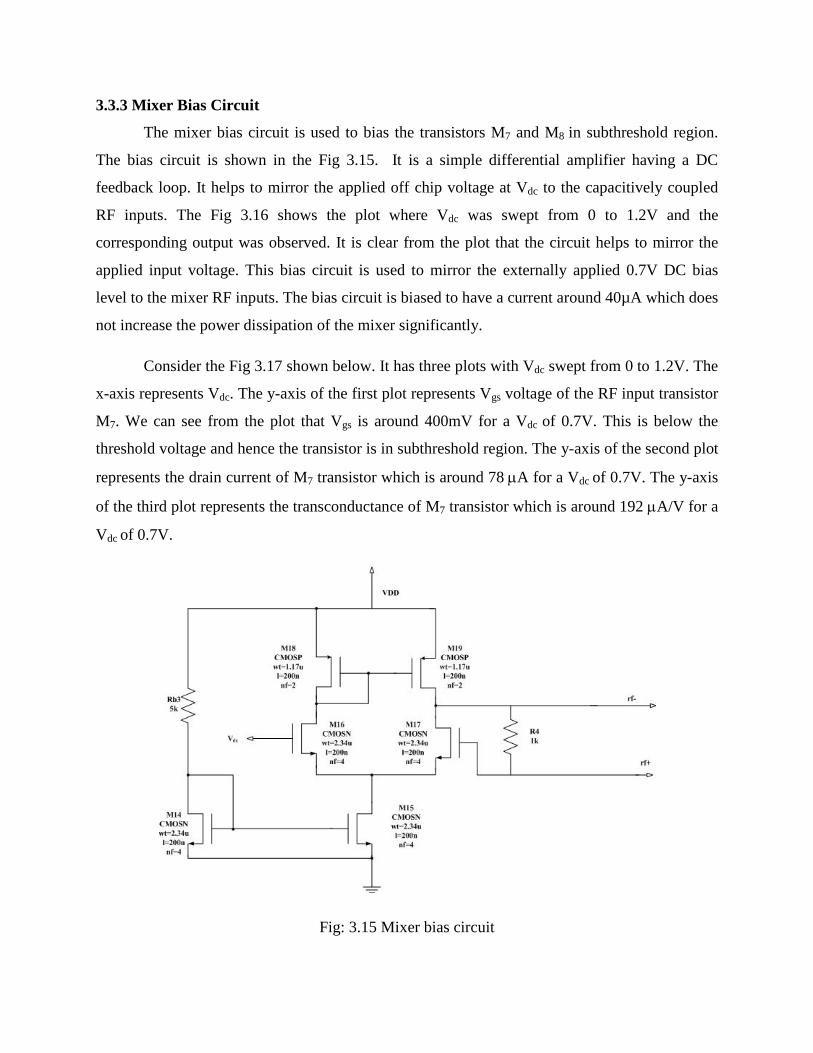
3.3.3 Mixer Bias Circuit
The mixer bias circuit is used to bias the transistors M7 and M8 in subthreshold region.
The bias circuit is shown in the Fig 3.15. It is a simple differential amplifier having a DC
feedback loop. It helps to mirror the applied off chip voltage at Vdc to the capacitively coupled
RF inputs. The Fig 3.16 shows the plot where Vdc was swept from 0 to 1.2V and the
corresponding output was observed. It is clear from the plot that the circuit helps to mirror the
applied input voltage. This bias circuit is used to mirror the externally applied 0.7V DC bias
level to the mixer RF inputs. The bias circuit is biased to have a current around 40µA which does
not increase the power dissipation of the mixer significantly.
Consider the Fig 3.17 shown below. It has three plots with Vdc swept from 0 to 1.2V. The
x-axis represents Vdc. The y-axis of the first plot represents Vgs voltage of the RF input transistor
M7. We can see from the plot that Vgs is around 400mV for a Vdc of 0.7V. This is below the
threshold voltage and hence the transistor is in subthreshold region. The y-axis of the second plot
represents the drain current of M7 transistor which is around 78 µA for a Vdc of 0.7V. The y-axis
of the third plot represents the transconductance of M7 transistor which is around 192 µA/V for a
Vdc of 0.7V.
Fig: 3.15 Mixer bias circuit

Fig 3.16 Plot showing that the mixer bias circuit mirrors the applied off chip voltage Vdc
Fig 3.17 Plot showing Vgs , drain current and transconductance of RF input transistor M7 with the
mixer bias voltage Vdc being swept between 0 and 1.2V.

3.4 Power Amplifier Power amplifier is used for the amplification of the small input RF power to a large
output RF power. In this work power amplifier can be considered as an amplifier which has been
optimized in terms of its ability to deliver power to a load in an efficient manner.
3.4.1 Efficiency and Gain
The important power amplifier performance metrics are efficiency and gain. Efficiency
describes how well an amplifier can convert DC input power to RF output power. This is
referred to as the DC-to-RF power conversion efficiency. More often this is referred to as the
drain efficiency. Drain efficiency can be defined mathematically as the ratio of the average RF
output power to the DC input power.
𝐷𝐸 = 𝜂 = 𝑃𝑂𝑈𝑇,𝑅𝐹𝑃𝐼𝑁,𝐷𝐶
(3.6)
Gain refers to how well an amplifier can convert input RF power to output RF output
power. Power gain can be defined as the ratio of the average RF output power to the average RF
input power.
𝐺 = 𝑃𝑂𝑈𝑇,𝑅𝐹𝑃𝐼𝑁,𝑅𝐹
(3.7)
3.4.2 Power added efficiency
The quantity that characterizes an amplifier’s power gain and drain efficiency is known
as the power added efficiency (PAE). It is defined as the RF output power minus the RF input
power divided by the DC supply power.
𝑃𝐴𝐸 = 𝑃𝑂𝑈𝑇,𝑅𝐹−𝑃𝐼𝑁,𝑅𝐹𝑃𝐼𝑁,𝐷𝐶
(3.8)
It can also be re-written as
𝑃𝐴𝐸 = 𝐷𝐸 (1 − 1𝐺
) (3.9)
From the Eq. 3.9 it can be clearly seen that PAE depends on power gain and drain
efficiency. As the power gain becomes very large, the PAE approaches the drain efficiency.

3.4.3 Gain Compression
The amplifier’s deviation from its ideal linear gain curve refers to gain compression. 1-
dB gain compression point is generally used for the characterization of the amplifiers. The 1-dB
compression point can be defined as the point of the input-output transfer characteristics where
the actual gain is 1-dB below the ideal liner gain. It represents an arbitrary upper limit of the
input signal for which the amplifier approximates the linear operation. This condition is shown in
the Fig. 3.16.
3.4.4 Total Harmonic Distortion
Total harmonic distortion (THD) is a very common method used for characterizing an
amplifier’s non-linearity. If the input to the amplifier is a single tone, a cosine wave signal
cos(ω0t), then the output will be:
𝑉𝑂𝑈𝑇 = 𝑎0 + 𝑎1 cos(ω0𝑡) + 𝑎2 cos(ω0𝑡)2 + 𝑎3 cos(ω0𝑡)3 + …. (3.10)
We know that raising a cosine of frequency ω0 to a power n will create a harmonic at a
frequency nω0 plus other spectral components. Therefore, the degree of non-linearity of an
amplifier can be characterized by the analyzing the spectral components in the output signal,
when the input is driven by a clean sine wave. This test is the basis for the measurement of
THD. The THD is given as
𝑇𝐻𝐷 = Σ𝑃𝐻𝑎𝑟𝑚𝑜𝑛𝑖𝑐𝑠𝑃𝐹𝑢𝑛𝑑𝑎𝑚𝑒𝑛𝑡𝑎𝑙
(3.11)
where PHarmonics is the total signal power and PFundamental is the total fundamental signal power.

Fig: 3.16 Pout vs. Pin for a generic linear amplifier [Terry]
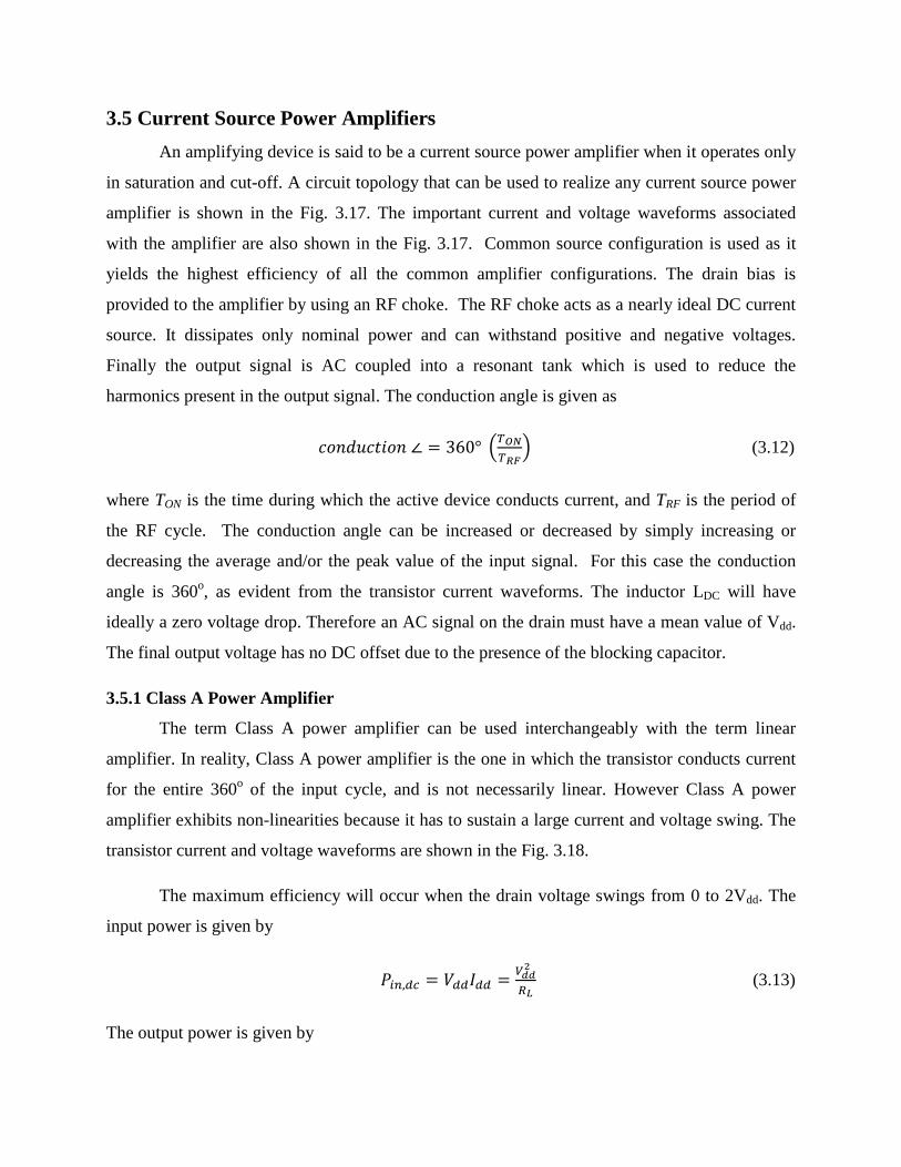
3.5 Current Source Power Amplifiers An amplifying device is said to be a current source power amplifier when it operates only
in saturation and cut-off. A circuit topology that can be used to realize any current source power
amplifier is shown in the Fig. 3.17. The important current and voltage waveforms associated
with the amplifier are also shown in the Fig. 3.17. Common source configuration is used as it
yields the highest efficiency of all the common amplifier configurations. The drain bias is
provided to the amplifier by using an RF choke. The RF choke acts as a nearly ideal DC current
source. It dissipates only nominal power and can withstand positive and negative voltages.
Finally the output signal is AC coupled into a resonant tank which is used to reduce the
harmonics present in the output signal. The conduction angle is given as
𝑐𝑜𝑛𝑑𝑢𝑐𝑡𝑖𝑜𝑛 ∠ = 360° 𝑇𝑂𝑁𝑇𝑅𝐹
(3.12)
where TON is the time during which the active device conducts current, and TRF is the period of
the RF cycle. The conduction angle can be increased or decreased by simply increasing or
decreasing the average and/or the peak value of the input signal. For this case the conduction
angle is 360o, as evident from the transistor current waveforms. The inductor LDC will have
ideally a zero voltage drop. Therefore an AC signal on the drain must have a mean value of Vdd.
The final output voltage has no DC offset due to the presence of the blocking capacitor.
3.5.1 Class A Power Amplifier
The term Class A power amplifier can be used interchangeably with the term linear
amplifier. In reality, Class A power amplifier is the one in which the transistor conducts current
for the entire 360o of the input cycle, and is not necessarily linear. However Class A power
amplifier exhibits non-linearities because it has to sustain a large current and voltage swing. The
transistor current and voltage waveforms are shown in the Fig. 3.18.
The maximum efficiency will occur when the drain voltage swings from 0 to 2Vdd. The
input power is given by
𝑃𝑖𝑛,𝑑𝑐 = 𝑉𝑑𝑑𝐼𝑑𝑑 = 𝑉𝑑𝑑2
𝑅𝐿 (3.13)
The output power is given by

𝑃𝑜𝑢𝑡,𝑅𝐹 = 𝑉𝑑𝑑2
2𝑅𝐿 (3.14)
Finally the drain efficiency can be calculated as
𝐷𝐸 =
𝑉𝑑𝑑2
𝑅𝐿
𝑉𝑑𝑑2
2𝑅𝐿
= 12 (3.15)
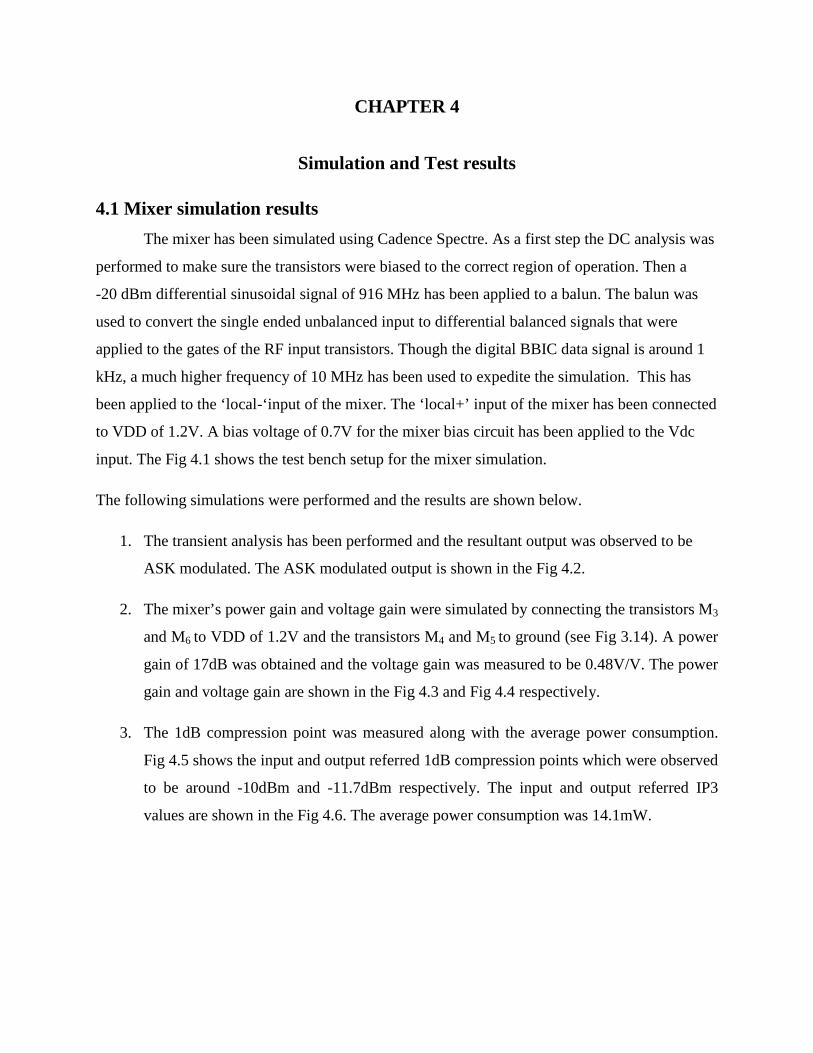
3.5.2 Class B Power Amplifier
The main drawback of Class A amplifier is that the active device dissipates significant
power compared to the peak RF output power. The active device can be biased such that it
conducts current for less than a full RF cycle so that the power dissipation can be reduced. In
other words we can drive the device into cutoff for some portion of the RF cycle. The Class B
power amplifier is biased to conduct current for only one-half of the RF cycle. The harmonics
are reduced using the tank circuit loading the amplifier. The current and voltage waveforms are
shown in Fig. 3.19. We can see that the drain current is only half of a sine wave.
The DC bias current can be found as the average value over one RF cycle of one half of a
sine wave
𝐼𝑑𝑑 = 1𝑇0∫ sin 2𝜋
𝑇0. 𝑡 𝑑𝑡 =
𝑇020
2𝜋𝑉𝑑𝑑𝑅𝐿
(3.16)
and the drain efficiency can be calculated as
𝐷𝐸 =
𝑉𝑑𝑑2
2𝑅𝐿
2
⎝
⎛𝑉𝑑𝑑2
𝜋𝑅𝐿
⎠
⎞
= 𝜋4≅ 0.785 (3.17)
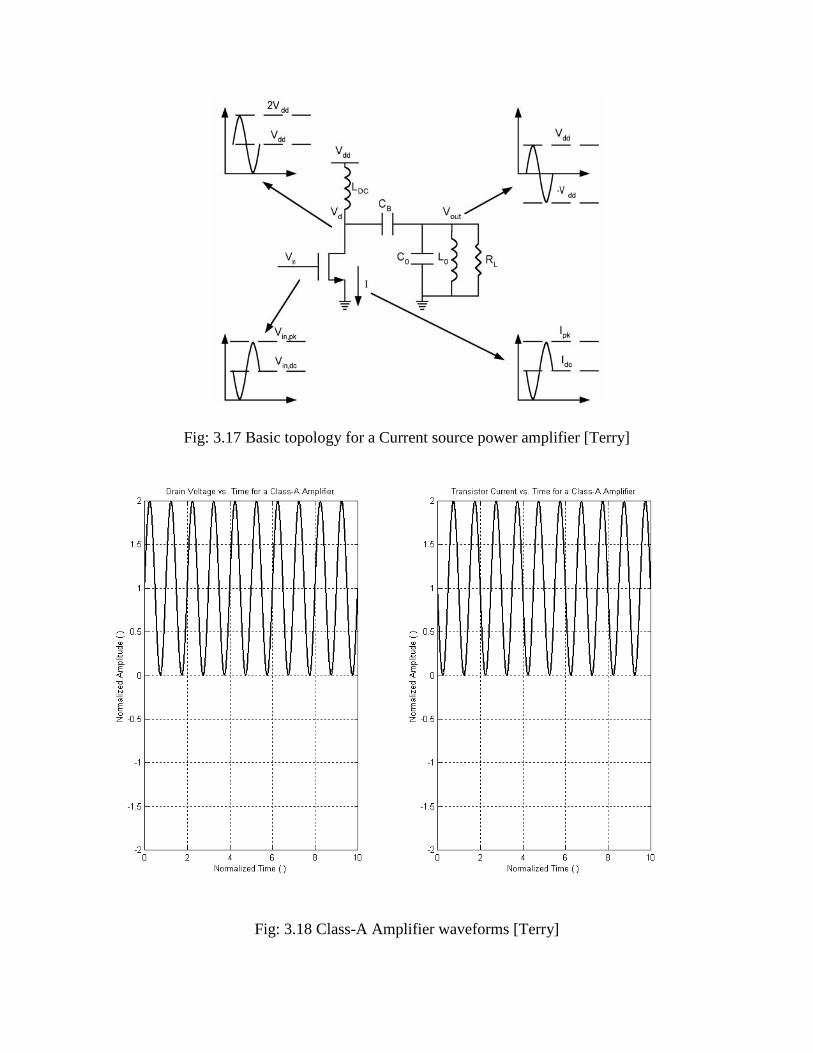
Fig: 3.17 Basic topology for a Current source power amplifier [Terry]
Fig: 3.18 Class-A Amplifier waveforms [Terry]
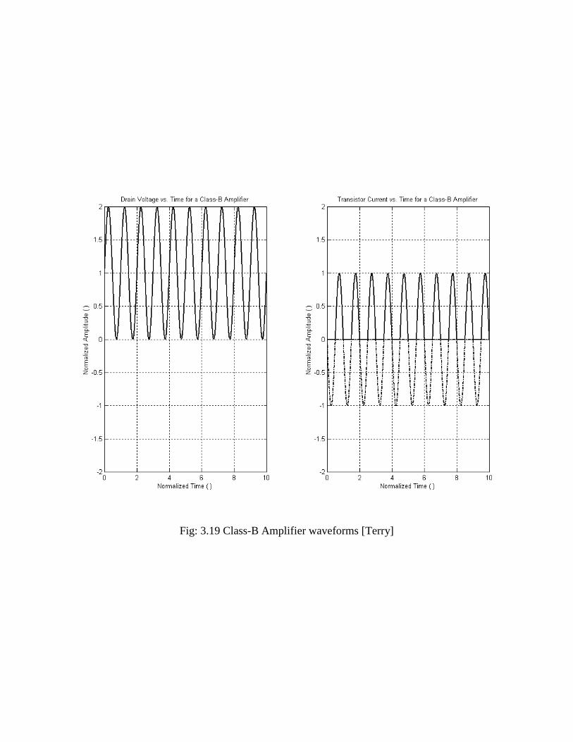
Fig: 3.19 Class-B Amplifier waveforms [Terry]

3.5.3 Class A-B Power Amplifier
Class B power amplifier trades efficiency for linearity. However it is desirable to have an
amplifier with better efficiency than the Class A amplifier, and better linearity than the Class B
amplifier. These specifications are met by Class A-B amplifier. The conduction angle for this is
somewhere between 180o and 360o. The efficiency lies between 0.5 and 0.785. The waveforms
are shown in Fig. 3.20. The conduction is halfway in between Class A mode and Class B mode.
3.5.4 Class C Power Amplifier
The previously discussed amplifiers can be used as linear amplifiers. But in applications
where efficiency is a priority Class C amplifier can be used. It has a conduction angle less than
180o and can achieve efficiencies greater than Class B amplifier. The transistor waveforms are
show in the Fig. 3.21.
The theoretical maximum efficiency is a function of the conduction angle and is given by
𝜂𝑚𝑎𝑥 = 2𝑦−𝑠𝑖𝑛2𝑦4(𝑠𝑖𝑛𝑦−𝑦𝑐𝑜𝑠𝑦) (3.18)
The efficiency can be increased arbitrarily towards unity. The parameter y is equal to the
conduction angle expressed as a percentage of the RF period.

Fig: 3.20 Class-AB Amplifier waveforms [Terry]

Fig: 3.21 Class-C Amplifier waveforms [Terry]

3.6 Power Amplifier Design The power amplifier considered in this BBIC design is a Class A power amplifier.
Though the efficiency is less compared to other amplifiers this amplifier was chosen for its
simplicity. As it is a Class A amplifier it operates for the entire 360° of the input cycle. The
output signal will also have the entire 360° phase like the input signal.
The schematic of the power amplifier is shown in the Fig 3.22. N0 and N1 transistors
provide the two stage amplification. The gate voltage of N0 and N1 is biased to about 1V and the
transistors operate in saturation region. The second harmonic distortion in the output signal will
be reduced by L2 and C2 which offer very high impedance to any second harmonic currents.

Fig: 3.22 Power amplifier
CHAPTER 4
Simulation and Test results
4.1 Mixer simulation results The mixer has been simulated using Cadence Spectre. As a first step the DC analysis was
performed to make sure the transistors were biased to the correct region of operation. Then a
-20 dBm differential sinusoidal signal of 916 MHz has been applied to a balun. The balun was
used to convert the single ended unbalanced input to differential balanced signals that were
applied to the gates of the RF input transistors. Though the digital BBIC data signal is around 1
kHz, a much higher frequency of 10 MHz has been used to expedite the simulation. This has
been applied to the ‘local-‘input of the mixer. The ‘local+’ input of the mixer has been connected
to VDD of 1.2V. A bias voltage of 0.7V for the mixer bias circuit has been applied to the Vdc
input. The Fig 4.1 shows the test bench setup for the mixer simulation.
The following simulations were performed and the results are shown below.
1. The transient analysis has been performed and the resultant output was observed to be
ASK modulated. The ASK modulated output is shown in the Fig 4.2.
2. The mixer’s power gain and voltage gain were simulated by connecting the transistors M3
and M6 to VDD of 1.2V and the transistors M4 and M5 to ground (see Fig 3.14). A power
gain of 17dB was obtained and the voltage gain was measured to be 0.48V/V. The power
gain and voltage gain are shown in the Fig 4.3 and Fig 4.4 respectively.
3. The 1dB compression point was measured along with the average power consumption.
Fig 4.5 shows the input and output referred 1dB compression points which were observed
to be around -10dBm and -11.7dBm respectively. The input and output referred IP3
values are shown in the Fig 4.6. The average power consumption was 14.1mW.

Fig: 4.1 Test bench setup for the simulation of mixer
Fig: 4.2 ASK modulated output obtained by performing transient analysis on the mixer

Fig: 4.3 Power gain of the mixer
Fig: 4.4 Voltage gain of the mixer

Fig: 4.5 1-dB Compression point of the mixer
Fig: 4.6 IP3 values of the mixer
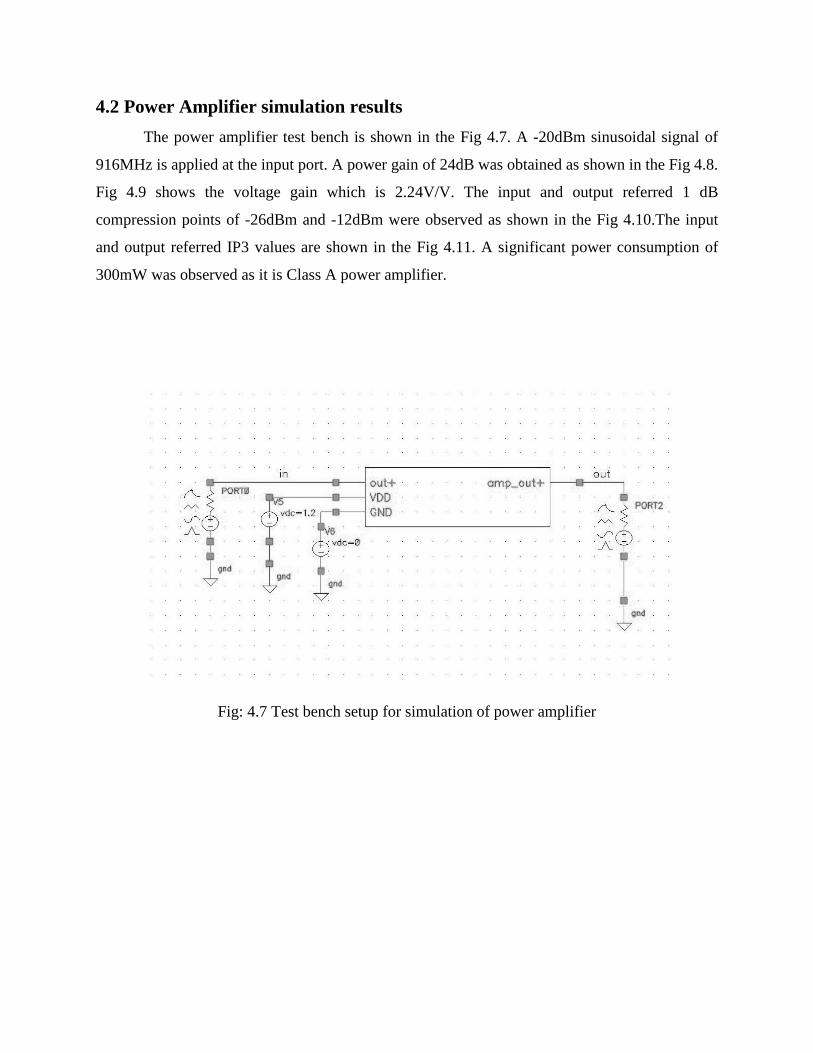
4.2 Power Amplifier simulation results The power amplifier test bench is shown in the Fig 4.7. A -20dBm sinusoidal signal of
916MHz is applied at the input port. A power gain of 24dB was obtained as shown in the Fig 4.8.
Fig 4.9 shows the voltage gain which is 2.24V/V. The input and output referred 1 dB
compression points of -26dBm and -12dBm were observed as shown in the Fig 4.10.The input
and output referred IP3 values are shown in the Fig 4.11. A significant power consumption of
300mW was observed as it is Class A power amplifier.
Fig: 4.7 Test bench setup for simulation of power amplifier

Fig: 4.8 Power gain of the power amplifier
Fig: 4.9 Voltage gain of the power amplifier

Fig: 4.10 1-dB compression point of the power amplifier
Fig: 4.11 IP3 curves of power amplifier

4.3 Entire circuit simulation results The entire circuit containing the mixer followed by the power amplifier was simulated.
The test bench is shown in the Fig 4.12. A -20dBm sinusoidal signal of 916MHz was inputted to
a balun. The balanced differential output from the balun was connected to the RF inputs of the
circuit. The digital BBIC data signal of 10 MHz has been applied to the ‘local-‘input of the
circuit. The ‘local+’ input of the circuit has been connected to VDD of 1.2V. A bias voltage of
0.7V for the mixer bias circuit has been applied to the Vdc input. The circuit’s differential output
was coupled to a balun.
The following simulations were performed and the results are shown below.
1. The transient analysis was performed on the circuit and the amplified ASK modulated
signal is shown in the Fig 4.13.
2. The power gain and voltage gain were simulated by connecting the transistors M3 and
M6 to VDD of 1.2V and the transistors M4 and M5 to ground (see Fig 3.14). A power gain
of 28.14 dB was obtained and is shown in the Fig 4.14. A voltage gain of 1.632 V/V was
obtained and is shown in the Fig 4.15.
3. The input and output referred 1 dB compression point of -22dBm and -12dBm were
observed as shown in the Fig 4.16.The input and output referred IP3 values are shown in
the Fig 4.17. Average power dissipation of 600mW was observed.

Fig: 4.12 Test bench setup for the simulation of the entire circuit
Fig: 4.13 The amplified ASK modulated signal obtained by performing transient analysis

Fig: 4.14 Power gain of the entire circuit
Fig: 4.15 Voltage gain of the entire circuit

Fig: 4.16 1-dB Compression point of the entire circuit
Fig 4.17 IP3 values of the entire circuit

4.4 Input matching network The input matching network was designed and included on the test board. The quality of
the input matching network was measured with the scattering parameter measurements. The L-
type input matching network was used to match the circuit’s input impedance to the source
impedance of 50Ω. The load impedance of the circuit was almost equal to the 50Ω and hence an
output matching network was not used. The input scattering parameter S11 was -6.76dB and the
output scattering parameter S22 was -22dB at 916MHz. The S21 parameter gave the available
power gain at 916MHz which was 28dB. They are shown in Fig 4.18.
Fig: 4.18 S-parameters of the input matching network

References

[Eric] Bolton, Eric Keith, A CMOS microluminometer for use in a bioluminescent bioreporter
integrated circuit, Thesis (M.S.), University of Tennessee, Knoxville, 2001.
[2007 IEEE] Syed K. Islam et al., IEEE Transactions on circuits and systems, Vol. 54, No. 1,
January (2007).
[Lathi. B.P] Lathi.B.P, Communication Systems, New York, Wiley, 1968.
[Razavi] Behzad Razavi, RF Microelectronics, Prentice Hall, 1998.
[Cocuh] Leon W. Couch, Digital and analog communication systems, Macmillan Publishing
Company, 1990.
[Arya] Arya Behzad, Wireless LAN Radios – System definition to transistor design, Wiley,
2008.
[Mo] Zhang, Mo, A low power CMOS microluminometer and transmitter for bioluminescent
bioreporter integrated circuit (BBIC), Thesis (M.S.), University of Tennessee, Knoxville, 2003.
[Carr] Joseph J Carr, RF components and circuits , Oxford :Newnes, 2002.
[Jeremy] Everard Jeremy, Fundamentals of RF circuit design : with low noise oscillators, John
Wiley, c2001.
[YongWang] Ding, YongWang, High-linearity CMOS RF front-end circuits, Springer, 2005.
[Arnott] Arnott,James C, A PLL frequency synthesizer and Gilbert cell multiplier for a 916 MHz
ISM band transmitter realized in 0.5 [mu]m [i.e. micrometer] CMOS technology, Thesis (M.S.)--
University of Tennessee, Knoxville, 1999.
[J P Silver]
[Terry] Terry, Stephen Christopher, Development of a high-efficiency, low-power RF power
amplifier for use in a high-temperature environment, Thesis (M.S.)--University of Tennessee,
Knoxville, 2002.
[Hanil] http://ieeexplore.ieee.org.proxy.lib.utk.edu:90/stamp/stamp.jsp?tp=&arnumber=4266441

[P J Sullivan]
[Rudell]