Embed Size (px)
Citation preview
Supporting Information: Surface Dangling Bonds Are a Cause of B-
Type Blinking in Si Nanoparticles
Nicholas P. Brawand, Marton Voros and Giulia Galli
1 Bulk Defect Structure
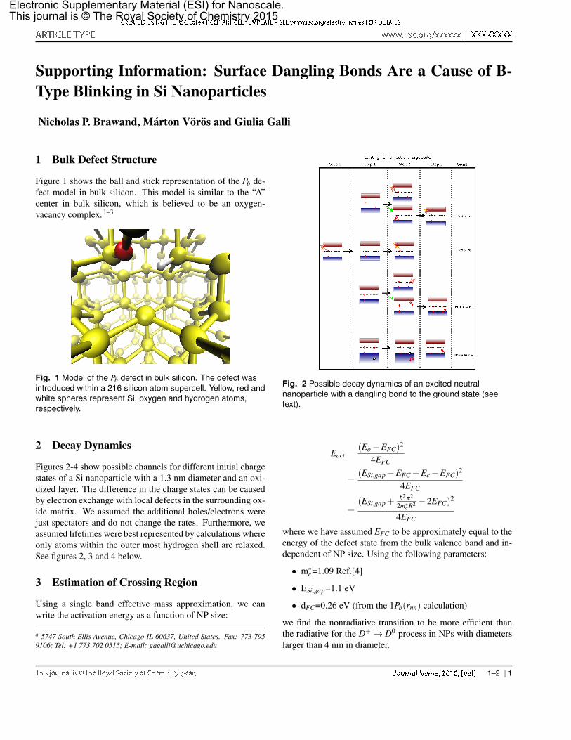
Figure 1 shows the ball and stick representation of the Pb de-
fect model in bulk silicon. This model is similar to the “A”
center in bulk silicon, which is believed to be an oxygen-
vacancy complex.1–3
Fig. 1 Model of the Pb defect in bulk silicon. The defect was
introduced within a 216 silicon atom supercell. Yellow, red and
white spheres represent Si, oxygen and hydrogen atoms,
respectively.
2 Decay Dynamics
Figures 2-4 show possible channels for different initial charge
states of a Si nanoparticle with a 1.3 nm diameter and an oxi-
dized layer. The difference in the charge states can be caused
by electron exchange with local defects in the surrounding ox-
ide matrix. We assumed the additional holes/electrons were
just spectators and do not change the rates. Furthermore, we
assumed lifetimes were best represented by calculations where
only atoms within the outer most hydrogen shell are relaxed.
See figures 2, 3 and 4 below.
3 Estimation of Crossing Region
Using a single band effective mass approximation, we can
write the activation energy as a function of NP size:
a 5747 South Ellis Avenue, Chicago IL 60637, United States. Fax: 773 795
9106; Tel: +1 773 702 0515; E-mail: [email protected]
Fig. 2 Possible decay dynamics of an excited neutral
nanoparticle with a dangling bond to the ground state (see
text).
Eact =(Eo −EFC)
2
4EFC
=(ESi,gap −EFC +Ec −EFC)
2
4EFC
=(ESi,gap +
h2π
2
2m∗
cR2 −2EFC)2
4EFC
where we have assumed EFC to be approximately equal to the
energy of the defect state from the bulk valence band and in-
dependent of NP size. Using the following parameters:
• m∗
c=1.09 Ref.[4]
• ESi,gap=1.1 eV
• dFC=0.26 eV (from the 1Pb(rnn) calculation)
we find the nonradiative transition to be more efficient than
the radiative for the D+→ D0 process in NPs with diameters
larger than 4 nm in diameter.
1–2 | 1
Electronic Supplementary Material (ESI) for Nanoscale.This journal is © The Royal Society of Chemistry 2015
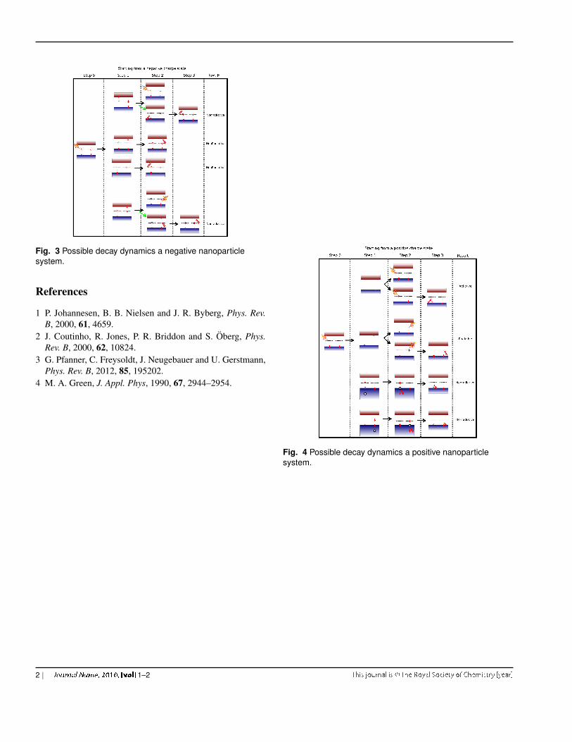
Fig. 3 Possible decay dynamics a negative nanoparticle
system.
References
1 P. Johannesen, B. B. Nielsen and J. R. Byberg, Phys. Rev.
B, 2000, 61, 4659.
2 J. Coutinho, R. Jones, P. R. Briddon and S. Oberg, Phys.
Rev. B, 2000, 62, 10824.
3 G. Pfanner, C. Freysoldt, J. Neugebauer and U. Gerstmann,
Phys. Rev. B, 2012, 85, 195202.
4 M. A. Green, J. Appl. Phys, 1990, 67, 2944–2954.
Fig. 4 Possible decay dynamics a positive nanoparticle
system.
2 | 1–2


![Molecular modeling and simulation of atactic polystyrene ... · simulated with MD and terminating dangling bonds at the surface as silanol groups, following ref [11]. Finally, to](https://img.dokumen.tips/doc/110x75/5c686faf09d3f27c028b719c/molecular-modeling-and-simulation-of-atactic-polystyrene-simulated-with.jpg)