Embed Size (px)
Citation preview

S1
Supporting Information
Reversible Positioning of Single Molecules inside Zero-Mode Waveguides
Joseph Larkin,† Mathieu Foquet,# Stephen W Turner,# Jonas Korlach,# and Meni Wanunu†*
†Departments of Physics and Chemistry/Chemical Biology, Northeastern University, Boston, Massachusetts 02115, United States,
#Pacific Biosciences, Menlo Park, California 94025, United States
*Corresponding Author

S2
Fabrication of NZMWs The starting substrate was a 175 µm-thick, 100 mm diameter, ‹100› silicon wafer. Prior to LPCVD, the wafers were cleaned with a standard RCA process, rinsed with deionized water, and spun dry. Next, they were immediately placed in a MRL Industries LPCVD furnace. 35 nm of SiNx was deposited on either side of the wafers (Figure S1, step 1). One side would eventually be SiNx membranes; the other would be used as a KOH etch mask to etch down to the membranes.
The next major step was e-beam lithography (EBL). The EBL process closely followed previously outlined protocols with negative e-beam resist.1 Wafers were first and negative e-beam resist NEB-31 was spun and baked (Figure S1, step 2). The ZMW pattern, which consisted of arrays of circles of nominal 80 nm diameter, was exposed in a JEOL 6300FS e-beam writer. In addition to the circles, two alignment marks were exposed in the resist. These would line up with photolithography marks later in the process to ensure that each ZMW array would be aligned with a SiNx membrane. After exposure the resist was baked developed in MF321 solution and immersed in two successive baths of deionized water. The samples were dried under a gentle stream of nitrogen. Before metallization, wafers were descummed in a 100 W downstream oxygen plasma (Figure S1, step 3). 100 nm of thermally evaporated aluminum was deposited immediately following the descum step (Figure S1, step 4). To lift off the e-beam resist and form ZMWs, the wafers were immersed for three hours in sonicated 1165 Remover solution heated to 68 °C. Following a thorough rinse in deionized water, the wafers were descummed once more in a 100 W oxygen plasma (Figure S1, step 5). Prior to photolithography on the wafer’s reverse side, ZMWs were inspected in a scanning electron microscope (SEM) to verify metallization, liftoff, and uniformity.
Following fabrication of ZMWs with EBL, photolithography was used on the other side of the wafer to define the pattern for KOH etching down to membranes. First, Shipley Microposit S1818 positive photoresist was spun on the non-ZMW side of the wafers (Figure S1, step 6). Resist was exposed in a Suss MicroTech MA/BA 6 contact aligner. A photomask with alignment marks was used. These marks were identical to those written during the EBL step. While the wafer is being aligned. After back side alignment, the resist was exposed and then developed in MicroDev for one minute (Figure S1, step 7). Next, the SiNx was etched with SF6 plasma in a Technics Micro-RIE Series 800 to expose windows of bare silicon for KOH etching down to free-standing SiNx ZMW membranes (Figure S1, step 8).
Before wet etching of silicon, it was essential to somehow protect the ZMW aluminum nanostructure from alkaline KOH etching solution. To accomplish this, the aluminum layer was covered with Brewer Scientific ProTEK B1-18. This polymer protects features from highly basic solutions, but may be removed with organic solvents after KOH etching. The ProTEK was spun onto the ZMWs at 2500 RPM for one minute, followed by successive bakes at 115 °C for two minutes and 205 °C for one minute (Figure S1, step 9). The wafer was then tightened between the o-rings of an Idonus PEEK backside protection wafer

S3
chuck to further protect the ZMWs from KOH. The sample was placed in 40% KOH at 60 °C for 8 hours to etch the exposed silicon squares down to silicon nitride membranes, each supporting an array of ZMWs (Figure S1, step 10). Following a thorough rinse in deionized water, the wafer was soaked for several hours in successive baths of methyl isoamyl ketone, n-methyl pyrrolidone, and isopropyl alcohol to remove the ProTEK. This process results in a wafer of roughly 200 chips, each with a free-standing SiNx membrane containing an array of ZMWs (Figure S1, step 11).
To use these chips for nanopore experiments, they will need to be treated with piranha solution (H2O2 : H2SO4 , 3:1 volume ratio) to hydrophilize the nanopore surface. As with the KOH, the ZMWs must be protected from this harsh chemical treatment. In order to do this, the ZMWs were coated with a 11 nm-thick layer of SiO2 by atomic layer deposition (ALD) at 250°C.2 The ALD layer coats the entire ZMW surface conformally, ensuring good chemical protection (SEE SI), but is still thin enough that a pore may easily be fabricated in it (Figure S1, step 12).

S4
Piranha cleaning of ZMW chips
Cleaning with piranha solution (1:4 H2O2:H2SO4) is essential to measuring stable open pore currents from small solid-state nanopores.3 Piranha, however strips metal from nanopore chips, as shown in Figure S2a. Therefore, in order to successfully integrate ZMWs into a solid state nanopore system, the metal of the ZMWs must be somehow protected from the piranha treatment. To do this, we have coated the ZMW surface with 11 nm of ALD.2 ALD coats an entire surface conformally, so a thin layer will penetrate a ZMW and coat the inside walls. This relatively thin layer is enough to protect ZMWs from piranha, as shown by the photos in Figure S2a, and the TEM image of an ALD-coated ZMW in Figure S2b after 5 minutes of immersion in heated piranha.
Figure S1. Schematic illustration of the steps of the NZMW fabrication process: 1. LPCVD silicon nitride coating of silicon wafer. 2. Spin NEB31 negative e-beam resist. 3. Expose and develop dots in resist. 4. Thermally evaporate 100 nm of aluminum. 5. Liftoff resist with sonication and soaking in solvent. 6. Spin S1818 positive photoresist on reverse side. 7. Expose and develop photoresist. 8. Etch silicon nitride windows with reactive ion etching. 9. Spin and bake protective ProTEK polymer on ZMW surface. 10. KOH etch silicon to expose free-standing membranes. 11. Remove ProTEK by soaking in solvent. 12. Deposit ALD SiO2.

S5
YOYO-1-labeled DNA traces In Figure S3, we show twelve ZMW traces from the experiment discussed in Figure 5 of the main text. The bottom trace is from a NZMW.
Figure S2. a) Photograph of four NZMW chips. The chips in the left column have no SiO2 coating, while the ones in the right column do. The chips in the top row have not had piranha treatment, while the chips in the bottom row have had five minutes of piranha treatment. The chip with no SiO2 has had nearly all of its Aluminum removed during piranha. The chip with SiO2 coating has no visible differnce from the untreated NZMW chips. b) A high resolution TEM image of a SiO2-coated ZMW after five minutes in piranha shows that the ZMW structure is intact.

S6
In Figure S4, we show the NZMW fluorescence trace along with the nanopore current. The discrete drops in current during fluorescence spikes illustrate pore blockage by DNA and eventual translocation. The coincidence of the drop in nanopore current and increase in fluorescence is illustrated by dashed lines in the figure. DNA is ejected by negative bias, as seen by drops in NZMW fluorescence upon voltage reversal.
Figure S3. Time traces of ZMW fluorescence with YOYO-labeled 6000 base pair DNA. The bottom trace is from a NZMW; the others are from conventional ZMWs. Spikes in fluorescence correspond to DNA capture into a given ZMW.

S7
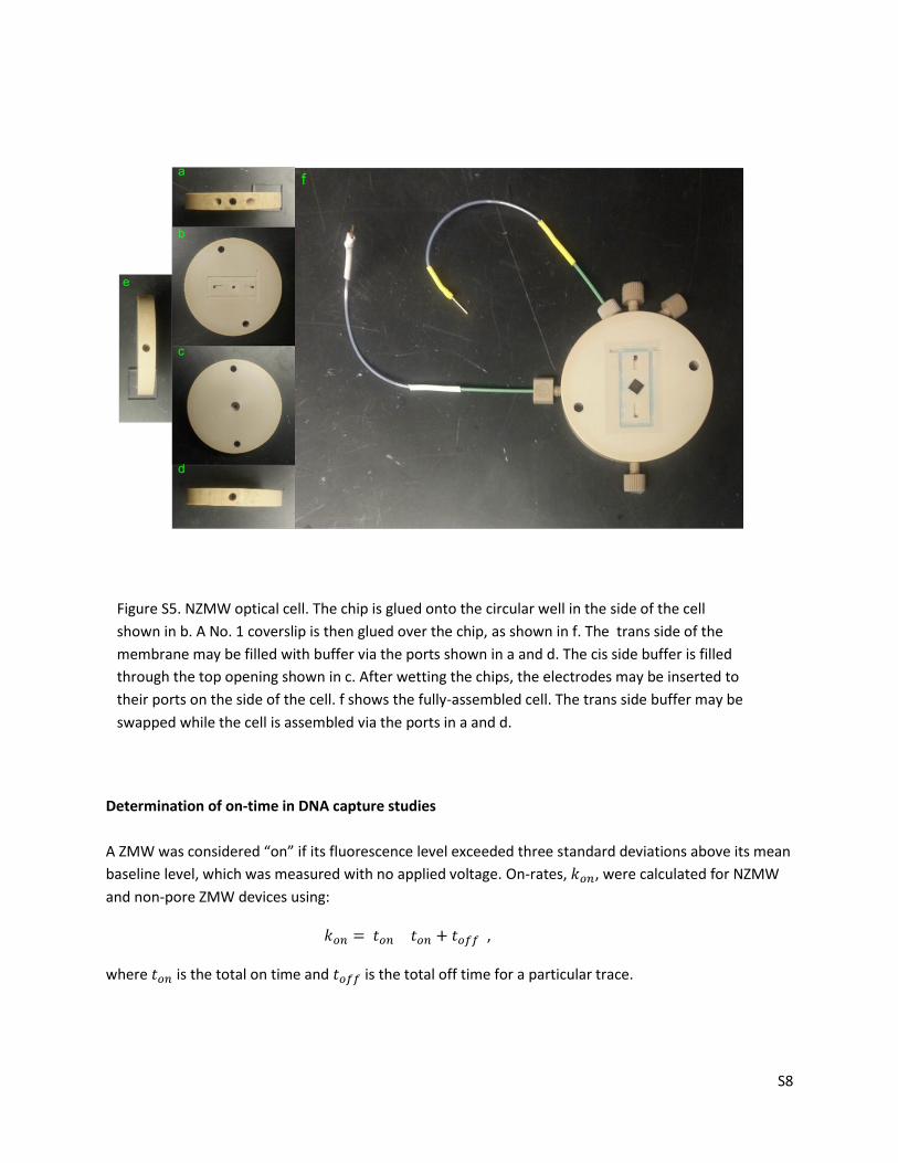
NZMW optical cell The NZMW chips were assembled in a custom-made PEEK cell, shown in the photos of Figure S5. The chips were glued to the cell with a quick-curing silicone paste (Smooth-On Ecoflex 5). A No. 1 glass coverslip was then glued over the chip with the same silicone elastomer. Following assembly, electrodes were screwed into the cell, as shown in Figure S5f. The cis and trans sides of the membrane were then filled with the desired buffer using syringes. The fully assembled cell was then screwed into a Faraday cage on an inverted fluorescence microscope with an integrated Axopatch 200 headstage for experiments.
Figure S4. Simultaneous time traces of nanopore current and ZMW fluorescence with YOYO-labeled 6,000 base pair DNA. Simultaneous current blockages and fluorescence spikes are identified with dashed lines.
S8
Determination of on-time in DNA capture studies A ZMW was considered “on” if its fluorescence level exceeded three standard deviations above its mean baseline level, which was measured with no applied voltage. On-rates, , were calculated for NZMW and non-pore ZMW devices using:
,
where is the total on time and is the total off time for a particular trace.
Figure S5. NZMW optical cell. The chip is glued onto the circular well in the side of the cell shown in b. A No. 1 coverslip is then glued over the chip, as shown in f. The trans side of the membrane may be filled with buffer via the ports shown in a and d. The cis side buffer is filled through the top opening shown in c. After wetting the chips, the electrodes may be inserted to their ports on the side of the cell. f shows the fully-assembled cell. The trans side buffer may be swapped while the cell is assembled via the ports in a and d.

S9
Gel electrophoresis of 4:1 DNA:streptavidin complex To show that streptavidin binds to our niotinylated DNA we incubated our 5’-biotin-1,003-bp DNA molecule with Alexafluor-647-labeled streptavidin (A647Stv) in a 4:1 DNA:Stv ratio for 15 minutes, followed by analysis using agarose gel electrophoresis (see Figure S6). We first imaged the red channel to show that A647Stv binds to the DNA (red-toned bands in the image), and then imaged the DNA after staining the gel with ethidium bromide. Even though a 4:1 DNA:Stv ratio was used, we found that the predominant complex formed had a 2:1 DNA:Stv stoichiometry, whereas much of the DNA remains unbound (labeled as 1:0 in the image). This excess of free DNA explains the presence of spikes in the electrical traces in Figure 3 for the DNA:Stv complex.
Figure S6. Agarose gel electrophoresis of a pre-incubated 4:1 stoichiometric complex of 1003-bp biotinylated DNA and Alexa 647-labeled streptavidin (A647Stv). To the right of the 1 kbp ladder we show the PCR-purified DNA, and to its right we show the 4:1 DNA:A647Stv complex. The red bands correspond to red fluorescence from the A647 label, whereas the greyscale image is a green channel following ethidium bromide staining.

S10
References
1) Foquet, M.; Samiee, K. T.; Kong, X. X.; Chauduri, B. P.; Lundquist, P. M.; Turner, S. W.;
Freudenthal, J.; Roitman, D. B. J Appl Phys 2008, 103.
2) Hausmann, D.; Becker, J.; Wang, S. L.; Gordon, R. G. Science 2002, 298, 402-406.
3) Wanunu, M.; Meller, A. Nano Lett. 2007, 7, 1580-1585.