Embed Size (px)
Citation preview
www.sciencemag.org/cgi/content/full/342/6155/224/DC1
Supplementary Materials for
Imaging Atomic Rearrangements in Two-Dimensional Silica Glass: Watching Silica’s Dance
Pinshane Y. Huang, Simon Kurasch, Jonathan S. Alden, Ashivni Shekhawat, Alexander
A. Alemi, Paul L. McEuen, James P. Sethna, Ute Kaiser, David A. Muller*
*Corresponding author. E-mail: [email protected]
Published 11 October 2013, Science 342, 224 (2013) DOI: 10.1126/science.1242248
This PDF file includes:
Materials and Methods Figs. S1 to S6 Captions for movies S1 to S5 References (38–40)
Other Supplementary Material for this manuscript includes the following: (available at www.sciencemag.org/cgi/content/full/342/6155/224/DC1)
Movies S1 to S5

2
Materials and Methods Transmission electron microscopy (TEM )Imaging
Transmission electron microscopy (TEM) samples were prepared by etching the copper growth substrate in 15% nitric acid and fishing the floating film onto commercial TEM grids (Quantifoil R1.2/1.3 holey carbon film on Au 200 mesh). Afterwards, the specimen was rinsed in distilled water and dried in nitrogen. Prior to TEM, the samples were heated in air at 200°C for 10 minutes.
High-Resolution TEM experiments were performed with an image-side corrected FEI Titan 80-300 microscope operated at 80kV. The spherical aberration was set to approximately 20 μm, with a -9 nm defocus (close to the standard Scherzer defocus). These imaging conditions provided good contrast and defocus range for both the graphene and silica. Experiments are conducted at room temperature. Atom Tracking
To identify the positions of atoms in each frame, we first cross-correlate the images to align them. The contrast from the graphene lattice is then mostly removed by Fourier filtering, as shown in Figures S2 and S3. Next, we obtain rough guesses of the atom positions using ImageJ to threshold the images and locate the centers of atomic sites (Si-O-Si columns).
The rest of the tracking and processing is conducted in Matlab. Our automatic thresholding identifies ~99% of atoms correctly in the 2D solid; the remaining ~1% misidentifications are obvious by eye and reflect our use of a global threshold to make the initial, rough determination of the atom positions. These errors result when the intensities of adjacent atoms overlap sufficiently: the thresholding will find only a single atom, and place it at their center-of-mass. To correct these errors, we manually remove features that are not isolated atoms and add atoms that were not found by thresholding. We then refine the atom positions by approximating Gaussian fits to the intensity of the image around each atomic site obtained from ImageJ. The above techniques give us lists of the 2D-projected centers of atomic sites in each frame.
Next, we use particle-tracking software developed by Grier, Crocker, and Weeks(31), implemented in Matlab by Blair and Dufresne (38). This software reads in our atom positions for all of the frames, then determines the best-fit identification for atoms across the entire video, and assigns each independent atom a unique identifier. From this output, we produce atom trajectories and displacements such as those in Figure 1 and Figure 3; the tracking data also makes it possible to measure the mean squared displacement of each atom (Figure 4E).
Strain Analysis We can quantify the elastic deformation using strain analysis, shown in Figure 2.
We measure strain relative to the initial configuration observed. We start with the displacement field u derived from our images and tracking data. To analyze elastic displacements, we first manually remove atoms that are undergoing bond-rotation. To simplify data processing, we then interpolate u (which only exists at each atom position)
3
onto a grid using a bicubic interpolation implemented in Matlab. We take its spatial derivative, producing the displacement gradient field:
X X
y y
u ux yu ux y
∂ ∂ ∂ ∂ ∇ =∂ ∂
∂ ∂
u
∇u can be separated into its symmetric component, the 2D strain tensor ε, and its anti-symmetric component, the local rotation matrix ω (32) . In linear elastic theory, the displacement gradient can be rewritten as
0
0xx xy
xy yy
∇ = + = + −
ε ε ωε ε ω
u ε ω ,
where Xxx
ux
∂=
∂ε , y
yy
uy
∂=∂
ε , and 12
yXxy yx
uuy x
∂ ∂= = + ∂ ∂
ε ε are components of the
strain tensor and 12
yX uuy x
∂ ∂= − ∂ ∂
ω gives the local rotation such that the rotation angle
arcsin( )=ϕ ω . Because our interpolated data is oversampled between atoms, we apply a Gaussian blur with σ~1.6 Å , or ½ of the in-plane Si-Si nearest neighbor spacing. Then, we crop the data to avoid edge effects. Finally, we plot the independent components of ε and ω in Figure 2.
Molecular Dynamics Simulations The molecular dynamic simulations in Figure 2 were carried out using LAMMPS
(33) . We used a parameterization of the Tersoff potential that was developed to study the structural properties of Si-O systems(39, 40). We first constructed “reference” structures representing the final positions in the 5-7-5-7 to 6-6-6-6 transition. Using conjugate gradients to find the ground state structure, this potential produced a Si-O bond length of 1.655 Å for the crystal. This result compares favorably with our experimental observations. The simulations shown in the main text were conducted at zero temperature; finite temperature simulations carried out at 300K produced similar results. To produce “large” systems for the strain fields in Figure 2 E-H and the displacement maps in Figure 2 I and K, we increased the size of the simulation box until the finite size effects were negligible ( > 9600 atoms; the final, “large” simulation cells comprised of 38400 atoms). To produce “amorphous” structures, we randomly switched bonds before relaxation. Finally, to model the ring exchange, we introduced a 5-7-5-7 ring (Stone-Wales type) defect into the reference structures and relaxed the new structure. This process produced the atom coordinates modeling our “before” and “after” structures. These atom coordinates were processed using the same atom-tracking techniques and strain measurements applied to our experimental data and described above.
4
Mean-squared displacements and coloring in Figure 4 A-D
The blue/yellow coloring in Figure 4 A-D was done by hand. The intensity of the red highlighting in Figure 4B-D represents the magnitude of the local volume change when compared to the initial frame. To create this coloring, we ran our atom tracking data through the strain analysis described in section 3 of the supplementary materials. Then we took the trace of the strain tensor (εxx+ εyy,), calculated by comparing the current frame atom positions to the first-frame atom positions. This strain component corresponds to volume change. We plotted its magnitude on a white-red scale, and then added it as a semi-transparent overlay to Figures 4 B-D. Because the strain can only be measured where the material is solid in both the initial frame and the frame of interest, we had to manually set its values where this was not the case. We set the color value to 0 (transparent) when it was outside of the solid in the current frame, and 1 (red) if it was liquid in the first frame, but solid in the current frame.
Next, we calculate mean squared displacement for different time intervals. First, we take all of the frame-to-frame positions for each atom in the entire video. Then, we calculate the mean displacement for each atom for each time interval Δt. For example, each atom in a 10 frame video would have 9 displacements for Δt=1 frame. Next, we use the positions determined by our edge-tracking algorithm (described below) to calculate each atom’s instantaneous distance from the nearest edge. Finally, we bin the data for all atoms by distance from the edge, and plot the results in Figure 4E.
Edge Tracking
The interface is defined as the region between the solid-like and liquid-like phases in which the frame-to-frame structures change from relatively static to quickly-varying. Our edge tracking algorithm approximates this by looking in each frame for a continuous line of tracked atoms with at least two in-plane nearest-neighbors (that are located within roughly a median bond-length). To determine the length of the edge of the solid silica and the enclosed area, we employ the following algorithm. We obtain the atomic coordinates using methods described above and in the main text. Starting with a blank bitmap the size of the original image, we draw lines connecting all nearest neighbors. We then fill in all enclosed pixels using Matlab’s imfill function. This filled-in area gives us the solid area, plotted in Figure S6. We obtain the pixels at the edge of this filled region using Matlab’s edge function. We then find the atoms and bonds (within our original coordinate and bond list) responsible for generating this edge. Since the “liquid-like” region can have non-bonded, but nearby atoms which should not be considered part of the bulk, we then remove all atoms that are only connected to a single atom, and repeat this 5 times, thus removing “dangling chains” of atoms at the edge. This gives us our final edge positions. We sum the bond-lengths of the remaining atoms to get the edge length, plotted in Figure S6. This procedure gives us good agreement with edge-structures determined by hand.

5
Fig. S1. Top and side-view cartoons of a bitetrahedral unit (left) and continuous disordered sheet (right). The mean Si-Si distance is 3.1 angstroms.
6
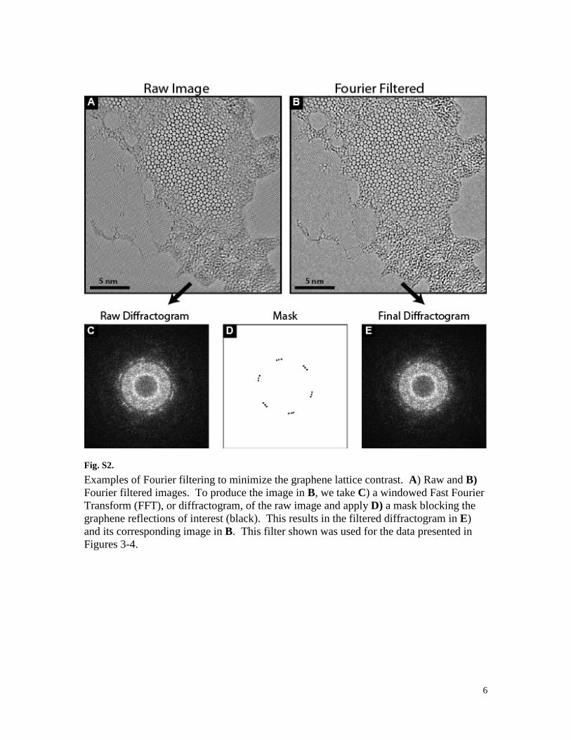
Fig. S2. Examples of Fourier filtering to minimize the graphene lattice contrast. A) Raw and B) Fourier filtered images. To produce the image in B, we take C) a windowed Fast Fourier Transform (FFT), or diffractogram, of the raw image and apply D) a mask blocking the graphene reflections of interest (black). This results in the filtered diffractogram in E) and its corresponding image in B. This filter shown was used for the data presented in Figures 3-4.

7
Fig. S3 Comparison of raw and processed images and tracking for the data in Figure 1. (A-B) Sample image and windowed Fast Fourier Transform (FFT) and (C-D) tracking data for raw, unprocessed video. (E-H) Corresponding data after Fourier filtering with a low-pass filter. The raw and filtered tracking data give similar results; G and H are reproduced from Figure 1.

8
Fig. S4 (bottom row) Best-fit elastic dipole. To produce the dipole, we used the elastic dipole tensor components, center position coordinates and a gaussian blur width as parameters in a least-squared fit to the experimentally observed strain components and (rotation field). For comparison, the top two rows, representing the strain and rotation fields from the experiment and atomistic simulation are reprinted from Figure 2. Scale bar is 1 nm. The right hand image shows a zoomed-out displacement field for the best-fit elastic dipole, with arrows enlarged ×2 for visibility.

9
Fig. S5 High-resolution TEM images from shearing region in Figure 3 and Movie S3. Colored markers are placed in the same locations from frame to frame to provide reference points for readers to follow the transformation. Scale bar is 2 nm.

10
Fig. S6 (A) Full initial image of the solid sheet used for analysis in Figure 4. The box indicates the region shown in Figure 4 A-D. Yellow and blue false-coloring indicate the locations of the solid-like and liquid-like phases. Scale bar 5 nm. (B) Plot of the relative area of the solid sheet (A/A0) and length of the phase interface (L/L0) versus time, taken from the full area shown in A. Each curve is normalized to its initial value. While frame-to-frame fluctuations are large, both the area and length remain, on average, near their initial values (See also Movies S4-5).

11
Movie S1 Annotated videos of ring rearrangement corresponding with Figure 1. (left) Video isolating the 5-7-5-7 to 6-6-6-6 ring rearrangement in Figure 1 B-E, with trajectories overlaid. (right) Larger view of area, corresponding with Figure 1 G-H. Each image has been smoothed, with graphene reflections removed. The fields of view: are 2.4 nm across (left) and 6.8 nm across (right). The original frame rate is 0.5 frames per second; movie is sped up 10x. All video formats are .avi with jpeg compression.
Movie S2 Unprocessed video containing regions from Movie S1. The full video in Movie S1 spans 14 images (28 s), for a total dose of ~5x10⁷ electrons/nm2. Original frame rate is 0.5 frames per second; movie is sped up 10x. The images are 7.5 nm across.
Movie S3 Video of shear region corresponding with Figure 3, with overlaid annotations matching those in Figure 3. Color overlay shows the four distinct regions with different motions in Figure 3; white boxes and colored dots indicate the three atoms highlighted in Figure 3 C-E. Each image is 13.5 nm across and has been smoothed, with the main graphene reflections suppressed. Original frame rate is 0.5 frames per second; movie is sped up 10x.
Movie S4 Video of entire interface in Figure S6, with a square indicating the region shown in Figure 4A-D. (37 frames at 2s intervals, total dose of 1 x10⁸ electrons/nm2). Movie is sped up 10x. The field of view is 14.8 nm across.
Movie S5 Unprocessed videos containing regions from Movies S3 and S4 (37 frames at 2s intervals, total dose of 1 x10⁸ electrons/nm2). Movie is sped up 10x. The field of view is 14.8 nm across.

12
References and Notes 1. M. L. Falk, J. S. Langer, Dynamics of viscoplastic deformation in amorphous solids. Phys.
Rev. E 57, 7192–7205 (1998). doi:10.1103/PhysRevE.57.7192
2. K. Maeda, S. Takeuchi, Computer simulation of deformation in two‐dimensional amorphous structures. Phys. Status Solidi 49, 685–696 (1978) (a). doi:10.1002/pssa.2210490233
3. M. L. Falk, C. E. Maloney, Simulating the mechanical response of amorphous solids using atomistic methods. Eur. Phys. J. B 75, 405–413 (2010). doi:10.1140/epjb/e2010-00157-7
4. M. L. Manning, J. S. Langer, J. M. Carlson, Strain localization in a shear transformation zone model for amorphous solids. Phys. Rev. E 76, 056106 (2007). Medline doi:10.1103/PhysRevE.76.056106
5. H. He, M. F. Thorpe, Elastic properties of glasses. Phys. Rev. Lett. 54, 2107–2110 (1985). Medline doi:10.1103/PhysRevLett.54.2107
6. P. Schall, D. A. Weitz, F. Spaepen, Structural rearrangements that govern flow in colloidal glasses. Science 318, 1895–1899 (2007). Medline doi:10.1126/science.1149308
7. W. K. Kegel, A. von Blaaderen, Direct observation of dynamical heterogeneities in colloidal hard-sphere suspensions. Science 287, 290–293 (2000). Medline doi:10.1126/science.287.5451.290
8. E. R. Weeks, J. C. Crocker, A. C. Levitt, A. Schofield, D. A. Weitz, Three-dimensional direct imaging of structural relaxation near the colloidal glass transition. Science 287, 627–631 (2000). Medline doi:10.1126/science.287.5453.627
9. A. S. Argon, H. Y. Kuo, Plastic-flow in a disordered bubble raft (an analog of a metallic glass). Mater. Sci. Eng. 39, 101–109 (1979). doi:10.1016/0025-5416(79)90174-5
10. P. Y. Huang, S. Kurasch, A. Srivastava, V. Skakalova, J. Kotakoski, A. V. Krasheninnikov, R. Hovden, Q. Mao, J. C. Meyer, J. Smet, D. A. Muller, U. Kaiser, Direct imaging of a two-dimensional silica glass on graphene. Nano Lett. 12, 1081–1086 (2012). Medline doi:10.1021/nl204423x
11. L. Lichtenstein, C. Büchner, B. Yang, S. Shaikhutdinov, M. Heyde, M. Sierka, R. Włodarczyk, J. Sauer, H. J. Freund, The atomic structure of a metal-supported vitreous thin silica film. Angew. Chem. Int. Ed. 51, 404–407 (2012). Medline doi:10.1002/anie.201107097
12. D. Löffler, J. J. Uhlrich, M. Baron, B. Yang, X. Yu, L. Lichtenstein, L. Heinke, C. Büchner, M. Heyde, S. Shaikhutdinov, H. J. Freund, R. Włodarczyk, M. Sierka, J. Sauer, Growth and structure of crystalline silica sheet on Ru(0001). Phys. Rev. Lett. 105, 146104 (2010). Medline doi:10.1103/PhysRevLett.105.146104
13. W. H. Zachariasen, The atomic arrangement in glass. J. Am. Chem. Soc. 54, 3841–3851 (1932). doi:10.1021/ja01349a006
14. L. Lichtenstein, M. Heyde, H.-J. Freund, Crystalline-vitreous interface in two dimensional silica. Phys. Rev. Lett. 109, 106101 (2012). Medline doi:10.1103/PhysRevLett.109.106101

13
15. M. Wilson, A. Kumar, D. Sherrington, M. F. Thorpe, Modeling vitreous silica bilayers. Phys. Rev. B 87, 214108 (2013). doi:10.1103/PhysRevB.87.214108
16. F. Ben Romdhane, T. Björkman, J. A. Rodríguez-Manzo, O. Cretu, A. V. Krasheninnikov, F. Banhart, In situ growth of cellular two-dimensional silicon oxide on metal substrates. ACS Nano 7, 5175–5180 (2013). Medline doi:10.1021/nn400905k
17. Materials and methods are available as supplementary materials on Science Online.
18. Z. Lee, K. J. Jeon, A. Dato, R. Erni, T. J. Richardson, M. Frenklach, V. Radmilovic, Direct imaging of soft-hard interfaces enabled by graphene. Nano Lett. 9, 3365–3369 (2009). Medline doi:10.1021/nl901664k
19. R. S. Pantelic, J. C. Meyer, U. Kaiser, H. Stahlberg, The application of graphene as a sample support in transmission electron microscopy. Solid State Commun. 152, 1375–1382 (2012). doi:10.1016/j.ssc.2012.04.038
20. E. Nakamura, Movies of molecular motions and reactions: The single-molecule, real-time transmission electron microscope imaging technique. Angew. Chem. Int. Ed. 52, 236–252 (2013). Medline doi:10.1002/anie.201205693
21. A. Hashimoto, K. Suenaga, A. Gloter, K. Urita, S. Iijima, Direct evidence for atomic defects in graphene layers. Nature 430, 870–873 (2004). Medline doi:10.1038/nature02817
22. J. C. Meyer, C. Kisielowski, R. Erni, M. D. Rossell, M. F. Crommie, A. Zettl, Direct imaging of lattice atoms and topological defects in graphene membranes. Nano Lett. 8, 3582–3586 (2008). Medline doi:10.1021/nl801386m
23. J. H. Warner, E. R. Margine, M. Mukai, A. W. Robertson, F. Giustino, A. I. Kirkland, Dislocation-driven deformations in graphene. Science 337, 209–212 (2012). Medline doi:10.1126/science.1217529
24. J. Kotakoski, J. C. Meyer, S. Kurasch, D. Santos-Cottin, U. Kaiser, A. V. Krasheninnikov, Stone-Wales-type transformations in carbon nanostructures driven by electron irradiation. Phys. Rev. B 83, 245420 (2011). doi:10.1103/PhysRevB.83.245420
25. J. Kotakoski, A. V. Krasheninnikov, U. Kaiser, J. C. Meyer, From point defects in graphene to two-dimensional amorphous carbon. Phys. Rev. Lett. 106, 105505 (2011). Medline doi:10.1103/PhysRevLett.106.105505
26. S. Kurasch, J. Kotakoski, O. Lehtinen, V. Skákalová, J. Smet, C. E. Krill, 3rd, A. V. Krasheninnikov, U. Kaiser, Atom-by-atom observation of grain boundary migration in graphene. Nano Lett. 12, 3168–3173 (2012). Medline doi:10.1021/nl301141g
27. S. G. Mayr, Y. Ashkenazy, K. Albe, R. S. Averback, Mechanisms of radiation-induced viscous flow: Role of point defects. Phys. Rev. Lett. 90, 055505 (2003). Medline doi:10.1103/PhysRevLett.90.055505
28. K. Zheng, C. Wang, Y. Q. Cheng, Y. Yue, X. Han, Z. Zhang, Z. Shan, S. X. Mao, M. Ye, Y. Yin, E. Ma, Electron-beam-assisted superplastic shaping of nanoscale amorphous silica. Nat. Commun. 1, 24 (2010). Medline doi:10.1038/ncomms1021
29. L. W. Hobbs, M. R. Pascucci, Radiolysis and defect structure in electron-irradiated α-quartz. J. Phys. Colloq. 41, C6-237–C6-242 (1980). doi:10.1051/jphyscol:1980660

14
30. P. M. Ajayan, S. Iijima, Electron-beam-enhanced flow and instability in amorphous silica fibres and tips. Philos. Mag. Lett. 65, 43–48 (1992). doi:10.1080/09500839208215146
31. J. C. Crocker, D. G. Grier, Methods of Digital Video Microscopy for Colloidal Studies. J. Colloid Interface Sci. 179, 298–310 (1996). doi:10.1006/jcis.1996.0217
32. B. A. Auld, Acoustic Fields and Waves in Solids (Wiley, New York, 1973).
33. S. Plimpton, Fast parallel algorithms for short-range molecular-dynamics. J. Comput. Phys. 117, 1–19 (1995). doi:10.1006/jcph.1995.1039
34. E. R. Grannan, M. Randeria, J. P. Sethna, Low-temperature properties of a model glass. I. Elastic dipole model. Phys. Rev. B 41, 7784–7798 (1990). Medline doi:10.1103/PhysRevB.41.7784
35. J. M. Howe, H. Saka, In situ transmission electron microscopy studies of the solid–liquid interface. MRS Bull. 29, 951–957 (2004). doi:10.1557/mrs2004.266
36. S. E. Donnelly, R. C. Birtcher, C. W. Allen, I. Morrison, K. Furuya, M. Song, K. Mitsuishi, U. Dahmen, Ordering in a fluid inert gas confined by flat surfaces. Science 296, 507–510 (2002). Medline doi:10.1126/science.1068521
37. J. Hernández-Guzmán, E. R. Weeks, The equilibrium intrinsic crystal-liquid interface of colloids. Proc. Natl. Acad. Sci. U.S.A. 106, 15198–15202 (2009). Medline doi:10.1073/pnas.0904682106
38. D. Blair, E. Dufresne, (The Matlab Particle Tracking Code Repository, at http://physics.georgetown.edu/matlab/).
39. J. Tersoff, Empirical interatomic potential for silicon with improved elastic properties. Phys. Rev. B Condens. Matter 38, 9902–9905 (1988). Medline doi:10.1103/PhysRevB.38.9902
40. S. Munetoh, T. Motooka, K. Moriguchi, A. Shintani, Interatomic potential for Si–O systems using Tersoff parameterization. Comput. Mater. Sci. 39, 334–339 (2007). doi:10.1016/j.commatsci.2006.06.010


![[Supplementary materials]](https://img.dokumen.tips/doc/110x75/56816583550346895dd82b8a/supplementary-materials-56cd0e37cc26b.jpg)