Embed Size (px)
Citation preview

Supplementary Figure 1. Roughness of Cu-BHT films with different thickness.
Supplementary Figure 2. GIXRD out-plane pattern different between thin film of 60 nm and thicker film of 200nm
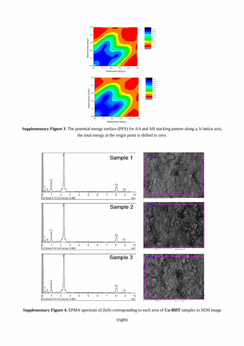
Supplementary Figure 3. The potential energy surface (PES) for AA and AB stacking pattern along a, b lattice axis,
the total energy at the origin point is shifted to zero.
Supplementary Figure 4. EPMA spectrum of (left) corresponding to each area of Cu-BHT samples in SEM image
(right)

Supplementary Figure 5. XPS full spectrum of Cu-BHT film
Supplementary Figure 6. IV-Curve of Cu-BHT film

Supplementary Figure 7 (a) Band structure and total density of state (DOS) for AA stacking pattern based on PBE
level (black line) and G0W0 level (red line). High-symmetry K points: Γ=(0,0,0), F=(0, 0.5,0), Q=(0,0.5,0.5),
Z=(0,0,0.5);(b) Band structure at PBE level for AB stacking pattern. High-symmetry K points: Z=(0.5,0,0),
Γ=(0,0,0), Y=(0,0,0.5), A=(0,-0.5,0.5), B=(0,-0.5,0), D=(0.5,-0.5,0), E=(0.5,-0.5,0.5), C=(0.5,0,0.5). The
Fermi level is at zero.
Supplementary Figure 8. Band structure and Density Of State (DOS) at (a)PBE,(b)LDA,(c) LDA+U(U=4),and (d)
LDA+U(U=6) level for single layer. K point Γ=(0,0,0), F=(0,0.5,0), Q=(0,0.5,0.5), Z=(0,0,0.5), X=(0.5,0,0), A=(0,-0.5,0.5),
F’=(0,-0.5,0), D=(0.5,-0.5,0), E=(0.5,-0.5,0.5), C=(0.5,0,0.5). The Fermi level is at zero.
K M
0
1
2
3
K M
0
1
2
3
K M
0
1
2
3
K M
0
1
2
3
Energ
y(e
V)
Wavevector
(a)
Total
Cu
S
C
DOS(/eV)
Energ
y(e
V)
Wavevector
(b)
Total
Cu
S
C
DOS(/eV)
Energ
y(e
V)
Wavevector
(c)
Total
Cu
S
C
DOS(/eV)
Energ
y(e
V)
Wavevector
(d)
Total
Cu
S
C
DOS(/eV)

Supplementary Figure 9. Theoretical predicted single layer topological structure (a), (b) and (c), top view (upper
panel) and side view (bottom panel).
Supplementary Table 1. Optimized crystal structure based on the minimum of potential energy surface for AA and AB
stacking with PBE-D2 functional.
Staking Pattern a b c
AA 8.748 8.748 3.539 77° 89.2° 120°
AB 8.748 8.748 6.82A 90° 90° 120°
Supplementary Table 2. Cu/S ratio calculated from EPMA.
Cu/S atom ratio
Sample1 0.5481
Sample2 0.5479
Sample3 0.5383

Supplementary Table 3.The Lattice parameters for crystal (a), (b) and (c) in Supplementary Figure 9.
Lattice
parameters a(Å) b(Å) c(Å) α(º) β(º) γ(º)
Space
group
Total
Energy/eV
Crystal (a) 9.39 9.39 14.9 90.00 90.00 120.00 P-6m2 -85.52
Crystal (b) 8.33 8.80 15.0 87.72 96.07 119.65 P1 -88.13
Crystal (c) 8.75 8.75 15.0 90.00 90.00 120.00 P6/MMM -90.05
Supplementary Note 1
Considering the EPMA data and mild reaction conditions, reaction product can be inferred with formula Cu3C6S6.
Indeed, we have employed Particle-swarm optimization (CALYPSO1) algorithm to predict possible crystal structure
with specific chemical composition. This method has been widely used in highly stable 2D nanostructures prediction2-5
.
Through thousands of possible structures screening and then structural optimization within the framework of density
functional theory as implemented in the Vienna Ab initio Simulation Package (VASP)6, several possible topological
structures have been proposed, as can be seen in Supplementary Fig. 9 and corresponding lattice parameters can be
found in Supplementary Table 3. It is obvious that Crystal (c) display the smallest total energy and then it is the most
stable one. In Addition, its lattice parameter and symmetry are much consistent with GIXRD data (as stated in
manuscript). Therefore, we have reasons to believe that Crystal (c) is the most likely topological structure.
Supplementary References
1 Wang, Y., Lv, J., Zhu, L. & Ma, Y. CALYPSO: A method for crystal structure prediction. Comput. Phys. Commun. 183,
2063-2070, (2012).
2 Luo, X. et al. Predicting Two-Dimensional Boron–Carbon Compounds by the Global Optimization Method. J. Am.
Chem. Soc. 133, 16285-16290, (2011).
3 Li, Y., Liao, Y. & Chen, Z. Be2C Monolayer with Quasi-Planar Hexacoordinate Carbons: A Global Minimum Structure.
Angew. Chem. Int. Ed. 53, 7248-7252, (2014).
4 Zhou, L.-J., Zhang, Y.-F. & Wu, L.-M. SiC2 Siligraphene and Nanotubes: Novel Donor Materials in Excitonic Solar Cells.
Nano Letters 13, 5431-5436, (2013).
5 Wu, X. et al. Two-Dimensional Boron Monolayer Sheets. ACS Nano 6, 7443-7453, (2012).
6 Kresse, G. & Furthmüller, J. Efficiency of ab-initio total energy calculations for metals and semiconductors using a
plane-wave basis set. Comput. Mater. Sci. 6, 15-50, (1996).