Embed Size (px)
Citation preview

Supertex inc.
Supertex inc. www.supertex.com
Doc.# DSAN-AN-H52A040413
AN-H52Application Note
IntroductionDevelopment of high-brightness light emitting diodes (LED) revolutionized the lighting industry in the recent years. Semiconductor light sources replace incandescent bulbs in an increasing number of applications due to their unsurpassed reliability and efficiency. Such applications include traffic signals, emergency lighting, hard-to-reach lighting fixtures, automotive lighting, accent and decorative lighting. Many of these applications demand off-line power drivers capable of regulated DC output current, low DC output voltage and input unity power factor.
A flyback converter can become a simple solution for these types of applications. When operating in discontinuous conduction mode, a flyback converter inherently provides a good power factor since the peak current in its inductor
is proportional to the instantaneous input voltage. However, a very large electrolytic smoothing capacitor is needed at the load in order to attenuate the rectified AC line ripple component of the output current. Low dynamic resistance of LEDs aggravates the problem even further. There are power topologies that can resolve this problem by cascading converter stages using a single active switch. Most of these topologies include an input boost converter stage for shaping the input current. Hence they require a transformer with a high step-down turn ratio in order to drive low voltage LEDs. A power transformer would be needed even when galvanic isolation of the output in not required. Overall power efficiency, cost and reliability can be improved by using a step-down buck-boost input stage.
D1
D4 L1
+
-
+
M1
C1D2
L2
D3 +CO LED
A simple transformerless power converter is shown in Fig.1. Its input buck-boost stage consisting of L1, C1, D1 and D4 is cascaded with an output buck stage including L2, D2, D3 and CO. Both converter stages share a single power MOSFET M1. The input buck-boost stage operates in discontinuous conduction mode (DCM), while the output buck stage runs in continuous conduction mode (CCM). Both converter stages can operate as step-down voltage converters. The overall step-down ratio is a product of the step-down ratios of the two converter stages. Thus a high step-down ratio is achieved without using a transformer. Steady-state voltage and current waveforms of this converter are shown in Fig.2. Switching the MOSFET M1 on applies the rectified AC line voltage across L1. Current in L1 rises linearly. At the same time, the bulk capacitor C1 powers the output buck stage.
(Note the negative polarity of the voltage across C1 with respect to ground when M1 is on.) The current in L2 ramps up. The current paths for this switching state are shown in Fig.3a.
When M1 turns off, D1 becomes forward-biased. The input inductor current diverts into C1. At the same time, the current in the output inductor L2 finds its way through D3. (See Fig. 3b.). The current in L1 ramps down. As soon as the current reaches zero, the diode D1 becomes reverse-biased and prevents the current in L1 from reversing. (The reverse current flow back into the input source would otherwise cause harmonic distortion of the input current and reduction in the overall efficiency.) Fig.3c depicts this switching state.
HV9931 Unity Power FactorLED Lamp Driver
Fig 1: Power conversion topology**This topology includes intellectual property of Supertex, Inc. A paid up license is offered for application of the HV9931 product.

2Supertex inc.
www.supertex.comDoc.# DSAN-AN-H52A040413
AN-H52
VL2
IL1
VL1
M1
0
0
0
0
0
ON
ILI(PK)
0
0
0
-VC3
VIN
0
OFF
ILI(PK)
-VC3
IL2(PK)
V0
IL2(PK)
I0
ID1
IL2
ID2
VIN + VC3
VDS(M1)
ILI(PK) + IL2(PK)
IM1
IL2(PK)
I0
ID3
VIN
Fig 2: Voltage and current switching waveforms

3Supertex inc.
www.supertex.comDoc.# DSAN-AN-H52A040413
AN-H52
D1
L1
D3
D1
D4
+
M1
C1
D2
L2
D3
LED
D4
L1
+
-
+
M1
C1
L2
D3 +
CO
LED
(a)
(b)
(c)
+
- +
CO
L2
LED
+
CO
+
M1
C1
+
-
D2
L1
D4
Fig 3: Switching states of the converter:(a) energizing L1 and L2, (b) de-energizing L1 and L2, (c) dead time of L1.
The value of the bulk capacitor C1 needs to be large enough to attenuate rectified AC line ripple. Then the duty cycle D and the switching frequency FS can be assumed constant over the AC line cycle. In this case, both the peak current IL1(PK) in L1 and the average input current IIN are directly proportional to the input voltage VIN. (See Fig. 4.) The factor
Reff = 2.L1.FS/D2 is the effective input resistance of the converter. This feature of the switching converter of Fig. 1 ensures low harmonic distortion of the input AC current and near-unity power factor. Other techniques using the HV9931 that can reduce harmonic distortion even further will be discussed below.

4Supertex inc.
www.supertex.comDoc.# DSAN-AN-H52A040413
AN-H52
VIN
TONTS =
1
FS
D = TON
= TON • FS TS
IL1(PK) = D • VIN
L1 • FS
IIN = 1
• D • IL1(PK) = 2
= D2
• VIN = 2L1 • FS
= VIN
REFF
LED Current Control LoopThe HV9931 is a peak current control IC that is specifically designed for optimally controlling the non-isolated single-stage PFC converter described above. A typical application circuit of the HV9931 is shown in Fig. 5.
Upon application of 12 - 450V at VIN, the built-in high voltage regulator circuit seeks to regulate 7.5V ± 5% at VDD. The circuit is equipped with an under-voltage protection comparator (UVLO) that inhibits switching until a threshold voltage is reached at VDD. A 0.5V hysteresis is included to prevent oscillation.
As soon the start-up threshold is reached at VDD, an internal oscillator circuit is enabled. The output signal of the oscillator triggers a PWM latch. The GATE output becomes high, the power MOSFET Q1 switches ON. The oscillator circuit can be programmed with a single resistor connected to RT for either constant switching frequency or fixed off-time operation. In the fixed off-time mode, the oscillator will set the PWM latch after a programmed time period following the turn-off of the GATE output. In order to program the HV9931 for constant frequency operation, the timing resistor needs to be connected between RT and GND. The switching frequency in this case can be calculated using the following equation: FS =
1 (1)
α • RT + τO
where α = 40pF, τO = 880ns. Connecting the resistor from RT to GATE programs constant off-time:
TOFF = α • RT + τO (2)
It can be shown that the fixed off-time operating mode: a) reduces the voltage stress at C1; b) improves input AC ripple rejection; c) inherently introduces frequency jitter that can help reduce the size of the input EMI filter required. Hence, we will assume the fixed off-time mode for the purpose of this discussion.
The control circuit further includes two comparators for programming peak currents in L1 and L2. Both comparators use the ground potential (GND) as a reference and can be used to monitor voltage signals of negative polarity with respect to GND. A blanking delay of 215ns is added to prevent false tripping the comparators due to the circuit parasitics. The currents iL1 and iL2 that trip the comparators can be computed as:
iL(PK) = VREF • RCS (3)
RREF • RS where VREF is an external reference voltage. We will use VREF = VDD as an example. When either of the comparators detects negative input voltage at its CS input, the PWM latch resets, the GATE output becomes low, and the MOSFET Q1
Fig 4: Waveforms explaining the unity power factor feature of the HV9931.

5Supertex inc.
www.supertex.comDoc.# DSAN-AN-H52A040413
AN-H52turns off. Note, that since L2 is assumed to operate in CCM:
iL2(PK) = iL2 + 1 • ∆iL2 (4)
2 where iL2 is the average current, and ΔiL2 is the peak-to-peak current ripple in L2. Thus the constant peak current control used in the HV9931 introduces a peak-to-average error
1/2ΔiL2 that needs to be accounted for when programming the resistor divider RREF2/RCS2. Fortunately, this error is nearly constant for any input voltage at fixed TOFF and it is relatively small compared to iL2 (15% typ.) Hence the ripple will have a minimal effect on the overall regulation of the output current. The error is however a function of the output voltage variation and the inductance value tolerances of L2.
VINC1
M1 D3
RREF2
D4
-
VO
+
7.5V
+ VC1 - iL2
S Q
R
D1
D2
~AC
CIN
OSC
REG
CDD
GND
PWMD
CS2
VIN
CS1
RT
GATE
VDD HV9931
L1 L2
RREF1
RCS1
RT
RS1
- VS1 +
RS2
- VS2 +
RCS2
iL1
~AC
-+
-+
Fig 5: Typical HV9931 off-line PFC LED Driver application circuit

6Supertex inc.
www.supertex.comDoc.# DSAN-AN-H52A040413
AN-H52
We need to design the input buck-boost stage to operate in DCM for any given line and load condition to ensure low distortion of the input current and stability of the control loop. Therefore, let us assume that the current in L1 becomes critically continuous at full load and some minimum operating AC line voltage VAC(MIN). Naturally, this boundary conduction mode (BCM) condition occurs at the peak of each half-wave of the input AC current. If we assume a unity power factor (PF = 1), this boundary condition will then coincide with the peak input voltage VAC(min) • √2. Since both converter stages are in CCM, the ratio between the output and the input voltage can be expressed as:
VO = DMAX • η1 • DMAX • η2 (5)
VAC(MIN) • √2 1 - DMAX
= D2
MAX • η 1 - DMAX
where η1 and η2 are the corresponding efficiencies of the input buck-boost stage and the output buck stage. The overall converter efficiency equals η = η1 • η2. The duty ratio D of the switch M1 is the greatest at this condition. (Duty ratio is defined as D = TON / TS, where TON is the on-time of M1, and TS is the switching period.)
The input AC line current can be obtained from the output LED current IO and the output voltage VO as:
IAC = VO • IO
(6) VAC • η
On the other hand, IAC • √2 =
D • IL1(PK) (7)
2
where the peak current IL1(PK) in L1 can be given as:
IL1(PK) = VAC • √2 • TON (8)
L1
Since our discussion is limited to the constant off-time case, let us express equation 8 in terms of TOFF = TON
• (1-D) / D: IL1(PK) =
VAC • √2 • TOFF • D
(9) L1 1 - D Finally, combining the equations (5), (6), (7) and (9) and solving for the inductance value gives:
L1 = VAC(MIN) • √2 • TOFF (10)
4 • IO (Note, that the critical inductance L1 corresponding to the boundary conduction at VAC(min) and Io is independent of the output voltage or the efficiency of the converter.)
The designer must be careful when considering standard inductors for L1 or designing a custom one. Since L1 conducts discontinuous current, magnetic flux excursion in the core material can be quite significant. Hence the design of L1 is limited by the power dissipation in the magnetic core material rather than by the saturation current of the inductor selected.
Designing C1Selecting the capacitance value for C1 is based on the input harmonics limits required for a specific application. Lighting products are sold in large quantities, and thus these high volume products can potentially have a high impact on the low voltage public supply system. The European EN 61000-3-2 Class C limits are comparable to the limits imposed by ANSI C82.77 standards in the U.S. market, and restrict overall current harmonics to approximately 33%. Both the Class C and ANSI standards limit the 3rd harmonic current of lighting products to ~ 30%. The regulations for LED-based traffic signal heads are generally stricter and require total harmonic distortion (THD) to be less than 20% (ITE VTCSH Part 2).
The prevalent component of the AC ripple voltage across C1 is the 2nd AC line harmonic. This ripple causes modulation of the duty cycle according to: D(t) =
VO (11) η2 • VC(t)
Power Converter Design
Designing L1

7Supertex inc.
www.supertex.comDoc.# DSAN-AN-H52A040413
AN-H52
where VC is voltage across C1. On the other hand, the input AC current can be expressed as:
IAC(t) = VAC • √2 • D(t)2 • TOFF • sin(2π • FAC • t) (12)
2L1 • (1 -D(t)) where FAC is the AC line frequency. Let us assume a small 2nd harmonics ripple voltage νC across C1, so that the voltage at C1 can be written as: VC(t) = VC - νC • sin(4π • FAC • t) (13)
where íC << VC. Substituting (11) and (13) in (12) will produce a displaced fundamental term and a 3rd harmonic term in the AC line current. It can be shown from the resulting equation that the 3rd harmonic distortion of the input AC line current for a given relative 2nd harmonic ripple KC = íC/VC <<1 is: K3 =
ΔI3rd ≈ 1 •
2 - D • KC (14)
IAC 2 1 - D Thus every 1% of 2nd harmonic ripple at C1 will generate at least 1% of 3rd harmonic component in the AC line current even when the duty cycle is small.
Let us determine the capacitance value of C1 needed to limit the 3rd harmonic distortion to some given K3. Equations (6), (7) and (9) together can be solved for the duty cycle D at any VAC within the operating range.
Let us introduce a parameter δ as follows: δ =
2 • V2AC • TOFF • η
(15) L1 • VO • IO Then the duty cycle can be expressed as:
D = 2 • (√1 + δ - 1)
(16) δ We can rewrite the equation (14) now as:
K3 = KC • 1 (17)
1 - 1 √1 + δ
Recalling that D = VO / (η2 • VC) and using (16), we can determine the voltage at C1 for a given VAC:
VC = VO • (1 + √1 + δ ) (18)
2 • η2
We have assumed that KC = íC/VC << 1. This condition is met by selecting C1 large enough so that the AC ripple voltage at C1 is low. Therefore, C1 decouples the bulk of the AC ripple current at the output of the input converter stage. Averaged over a switching cycle, this current can be written as:
I2(t) = VAC(t) • IAC(t) • η1 (19)
VC
where Vc is determined from (18). The AC line current IAC(t) is given by the equation (12). Then, under the assumptions made above, the AC component of I2(t) contains 2nd harmonic current only. This AC current in C1 can be expressed as:
IC(t) = - D2
• η1 • V
2AC • TOFF • cos(4π • FAC • t)
1 - D 2 • L1 • VC (20)
Substituting D and VC from (16) and (18) gives:
IC(t) = - 2 • IO • cos(4π • FAC • t) (21)
1 + √1 + δ
Relative ripple voltage at C1 can be calculated as KC = IC(PK) • ZC/VC, where IC(PK) is the amplitude of IC(t) and ZC = (4π • FAC • C1)-1 is the impedance of C1 at 2 • FAC. Substituting VC from (18), we obtain: IC(t) =
1 •
η2 • IO (22) (1 + √1 + δ)2
π • FAC • C1 • VO
Solving the equation (22) for C1 and substituting KC from (17) we get:
(23)
D = VO • IO • L1 V2
AC • TOFF • η • 1 + - 1 V2AC • TOFF • η
VO • IO • L1
1C1 =
η2 • IO
π • FAC • K3 • VO11 +1
δ • δ+[ ]

8Supertex inc.
www.supertex.comDoc.# DSAN-AN-H52A040413
AN-H52The RMS value of the switching current in C1 can be calculated using the following equation:
(23a)
The RMS value of the second AC line harmonic is derived from (21):
IC(LINE) = IO • √2 (23b)
1 + √1 + δ Using Non-Electrolytic Capacitors for C1The lifetime and the reliability of high brightness LEDs is remarkable. However, unlike incandescent light sources, LEDs generate conducted heat that needs to be dissipated within the lighting fixture. A power supply will be expected to function at elevated temperatures and match the lifetime of the LEDs when such power supply is integrated within the LED fixture. In many cases, this requirement rules out electrolytic capacitors commonly used in power supplies. As a “rule of thumb”, electrolytic capacitors suffer two times reduction of their life with every 10°C operating temperature rise. Therefore, it is desirable to be able to use a non-electrolytic capacitor for C1. Metallized polyester or PEN film capacitors can be considered for C1 as the most size and cost efficient replacement of aluminum electrolytic capacitors. However, they contribute a substantially higher cost per microfarad compared to electrolytic capacitors having similar voltage ratings. Thus, our design goal is to minimize the value of C1 while retaining low harmonic distortion.
As C1 becomes smaller, the condition of KC << 1 is no longer met. Thus, we cannot use the equation (14) for calculating the 3rd harmonic distortion coefficient K3. However, the equations (11) and (12) are still valid. We will combine these two equations and use VC(t) = VC + íC(t), where íC(t) is the AC ripple voltage at C1.
IAC(t) = VAC • √2 • VO
2 • TOFF 2L1 • η2 • (VC + vC(t))[(VC + vC(t)) • η2 - VO ]
• sin(2π • FAC • t) (24) We can see from the equation (24) that harmonic distortion of IAC(t) can be reduced by modulating TOFF as a function
of íC(t). In order to determine the modulation needed, we can expand the equation (24) in Taylor series in íC(t). Then we can negate the 1st order term of the resulting expansion in íC(t) by modulating TOFF inverse proportionally. This technique can achieve very good results since the linear term is responsible for the displaced fundamental and the bulk of 3rd harmonic in IAC(t).
One circuit implementation of this ripple cancellation feedback technique is shown in Fig.6. A charge pump circuit consisting of the capacitor CA and the diodes D5 and D6 performs level translation of VC to the ground potential. The voltage at C1 is reconstructed across the capacitor CB. The values of C B and the bleeder resistor RB are selected such that (2πRBCB)-1 >> 2 • FAC to preserve the ripple voltage íC(t). Capacitor CFF decouples the DC component of VC. The back-to-back connected Zener diodes D8 and D9 clamp the feedback voltage during initial charging of CFF. A proportional AC current íC(t)/RFF then modulates the off-time programmed by the RT pin of the HV9931.
TOFF(t) = α • (VRT - VD)
+ τO (25) VRT - VD -
vC(t) RT RFF where VD = 0.7V, VRT ≈ 6.5V. The capacitance value of CFF is selected such that (2πRFFCFF)-1 << 2 • FAC. Substituting TOFF(t) given by (25) in the 1st order Taylor series term of the equation (24) and solving it for RFF gives the feedback resistor needed to cancel harmonic distortion of the input AC current. RFF =
δ •
α • RT2 • VO
4 • √1 + δ η2 • (VRT - VD ) • (α • RT + τO ) (26)
(The derivation of the equation (26) has been omitted for the sake of simplicity.)
Note, the circuit of Fig.6 contributes a positive feedback whose gain must not exceed the negative feedback gain imposed by the equation (11) to avoid loop oscillation!
Therefore, perfect cancellation of harmonic distortion can only be achieved at a single point corresponding to the highest VO and VAC. Thus, the equation (26) must use
IC(SW) = IO • VAC • 2
64 VO
9 • π • η • η1+ D •

9Supertex inc.
www.supertex.comDoc.# DSAN-AN-H52A040413
AN-H52
VO(max) and VAC(max). Nevertheless, a dramatic reduction of C1 can still be achieved (up to several times depending on the input AC voltage range required).The designer must not forget another constraint limiting the minimum value of C1. The voltage at C1 must not fall below the output voltage (VC > VO) in order to avoid interruptions of the output current.
KC(MAX) < VC(MIN) - VO (27)
VC(MIN) Calculating L2Calculating the value of the output filter inductor L2 is simple. The designer must decide on the amount of switching ripple current in L2. Then: L2 =
VO • TOFF (28)
∆IL2 • η2
where ∆IL2 is the peak-to-peak current ripple in L2. Larger values of L2 will produce smaller ripple ∆IL2, and therefore smaller peak-to-average error in the output current control loop. However, it would also make the output current sense comparator more susceptible to noise. It is a good practice to design L2 for ∆IL2 = 0.2~0.3. An output capacitor can be added to reduce the output ripple current further if needed.Unlike the input inductor L1, design of L2 is typically limited by the saturation flux of its magnetic material. However, power dissipation due to the core loss may also need to be considered. The saturation current rating of the inductor
must satisfy:
ISAT > IO + 1 ∆IL2 (29)
2 Power Semiconductor ComponentsLet us calculate the voltage and the current ratings of the MOSFET M1 and the rectifiers D1-D4. The current in M1 is composed from the currents in the inductors L1 and L2. Hence, the RMS current in M1 can be computed as:
(30)
where IL1(PK) and Dmax are calculated from (9) and (16) at VAC(min). We disregarded the ripple current in L2 in the equation (30). The drain voltage rating of M1 can be determined as: VDS(M1) = VAC(MAX) √2 + VC(MAX) (1 +KC ) (31) where VC(max) and KC are calculated at VAC(max) using (18) and (22). It is very important to find a good balance between the total gate charge Qg and the on resistance RDS(ON) of the power MOSFET M1. Using the MOSFET with lower RDS(ON) will not necessarily achieve greater efficiency. The HV9931 has a gate driving capability mainly limited by the power dissipation in the high voltage regulator. In addition to generating higher switching power loss, MOSFETs with high Qg will require more current from the regulator. Non-optimal selection of M1 may cause the HV9931 to overheat.
ID(M1) = DMAX • IL1(PK)2 + DMAXIO
2
6
RT
GATE
VIN
L1 L2C1
M1 D3
RS1 RS2
D4
-
VO
+
D1 D2
~AC ~AC
CIN
RT
RFF
CFF
CB
CA
RB
D5 D8
D9
D6
D5
HV9931
Fig 6: Feedback circuit improving the power factor and THD

10Supertex inc.
www.supertex.comDoc.# DSAN-AN-H52A040413
AN-H52The highest currents in D1-D4 averaged over the AC line cycle can be calculated as:
ID1 = 4 • √2
• IO (32)
π η1 • (1 + √1+ δMIN ) ID2 = DMAX • IO =
2 • (√1 + δMIN - 1) • IO (33)
δMIN
ID3 = (1 - DMIN) • IO = (√1 + δMAX - 1)2
• IO (34) δMIN
(35)
where δMAX and δMIN are calculated from (15) at VAC(MAX) and VAC(MIN) correspondingly. Peak currents in D1 and D4 equal to IL1(PK) determined from (9) at VAC(MIN). Peak currents in D2 and D3 are computed as IO + ½∆IL2. The voltage ratings for D1-D3 are given as:
VR(D1) = VAC(MAX) √2 + VC(1 + KC ) (36)
VR(D2) = VAC(MAX) √2 (37)
VR(D3) = VC (1 + KC ) (38)
where VC and KC are calculated at VAC(MAX) from the equations (18) and (22).
The required reverse voltage rating of D4 depends on several factors. The dead time switching state of Fig.3(c) is characterized by a post-conduction resonance. The LC tank is formed by L1 and the parasitic capacitance of D1, D4 and M1. The resonant period can be estimated as: (39)
where COSS is the output capacitance of M1, Cj1 and Cj4 are reverse-biased junction capacitances of D1 and D4
correspondingly. Due to a finite reverse recovery time of D1, the input inductor L1 develops certain reverse current in the beginning of the dead time. Since L1 runs in DCM, reverse recovery of D1 is negligible from the overall power efficiency standpoint. However, even a small reverse current in L1 can cause a very high voltage spike across D4 when both diodes stop conducting. Thus, ultra fast recovery rectifier is recommended for D1.
Since Cj4<<COSS typically, the post-conduction oscillation occurs mainly across D4. The drain voltage of M1 will remain almost unchanged throughout the dead time. Besides causing the high voltage stress across D4, this oscillation may affect the EMI performance of the circuit. Thus, adding an RC snubber circuit across D4 is recommended. If the snubber capacitance value is greater than (COSS+Cj1), the reverse voltage rating of D4 can be reduced significantly. A fast 400V rectifier can be used for D4 in a universal 90-260VAC LED driver with adequate selection of the RC snubber components.
Using ultra-fast recovery rectifiers for D2 and D3 is essential for good efficiency of the LED driver. Both diodes operate at high current and are subjected to fast transitions and high reverse voltage.
PWM And Linear DimmingMany LED applications require dimming. Two types of dimming are available: analog and PWM. With analog (or linear) dimming, 50% brightness is achieved by applying 50% of the maximum current to the LED. Drawbacks to this method include LED color shift and the need for an analog control signal, which is not sometimes readily available. PWM dimming is achieved by applying full current to the LED at a reduced duty cycle. For 50% brightness, full current is applied at a 50% duty cycle. The frequency of the PWM signal must be above 100 Hz to ensure that the PWM pulsing is not visible to the human eye. The maximum PWM frequency depends upon the power-supply startup and response times. The HV9931 features a PWMD enable input that accepts a PWM dimming control logic signal. The GATE output is disabled when this signal is low. At the same time, since M1 is off and the rectifier D4 is reverse biased there is no discharge path for C1. Hence the current in L2 will recover within a single switching cycle back to its original level with no overshoots as soon as the PWMD signal becomes high again.
ID4 = 4 • √2 •
π 2 • √2 + 1 • IO δMIN η1 • (1 + √1+ δMIN )
TR = 2π L1 • Cj4(COSS + Cj1 )
COSS + Cj1 + Cj4

11Supertex inc.
www.supertex.comDoc.# DSAN-AN-H52A040413
AN-H52
Fig 8. Linear dimming circuit maintaining constant voltage at C1
VDD
CS2
RREF2
RCS2
RT
GATE
RTRB
RA
SW1
SW2
to M1 (GATE) to +VO
HV9931
In some cases, however, linear dimming is preferred for simplicity and component count reduction when the PWM control signal is not available. On the first glance at the HV9931, merely programming the divider ratio of RREF2 and RCS2 can control the output LED current proportionally. However, this method would affect the required voltage ratings of C1, M1 and D1-D4. The problem can be explained by the power imbalance between the input DCM and the output CCM converter stages. The DC voltage conversion ratio of the output buck stage is given by (11). Hence the duty cycle of the CCM buck stage is independent of the output current. On the other hand, the input buck-boost stage delivers an amount of energy every switching cycle that is a function of the duty ratio and the switching frequency. The balance is achieved by increased voltage at C1 for smaller output currents. The voltage stress can be very significant for universal 90 - 260VAC input designs. Fig.7 shows VC as a function of the output current based on the equation (18) for the universal LED driver given in
the Design Example section of this application note. (Note that VC exhibits no further increase as the output buck stage enters DCM.) Thus, the linear dimming method will require significantly higher voltage ratings of the switching components. The voltage stress problem at light load can be resolved by making TOFF proportional to IO. The equation (18) will no longer be load dependent since δ = const when TOFF/IO = const. One possible implementation of this dimming technique is depicted in Fig. 8. The timing resistor is altered in proportion with the output divider ratio. In order to maintain constant VC, the resistor values must satisfy:
Ra = Rb (40)
RCS2 RT However, the designer must be careful when using this technique, since, for example, linear dimming to 33% of the nominal load will cause the switching frequency of the converter to triple.
Fig 7. Voltage at C1 as a function of the output current in the case of linear dimming.
0 0.2 0.4 0.6 0.8
500
400
300
200
100
LED Current (A)
C1
Volta
ge (V
)
DCM
CCM
12Supertex inc.
www.supertex.comDoc.# DSAN-AN-H52A040413
AN-H52Phase-Control DimmingOne of the main advantages of the HV9931 LED driver solution is its inherent compatibility with phase-control dimmers. Solid-state light dimmers have been around since the 1960’s. They work by varying the duty cycle of the full AC voltage that is applied to the lights being controlled. Typical light dimmers are built using thyristors, and the exact time when the thyristor is triggered is relative to the zero crossings of the AC power. When the thyristor is triggered it keeps conducting until the current passing though it goes to zero.
Typical switch-mode LED drivers do not work well with phase-control dimmers because of the large output capacitance that they must use to filter the 2nd AC line harmonic ripple. Interruptions of the voltage at the output of a phase dimmer would have no effect on the output current of these LED drivers.
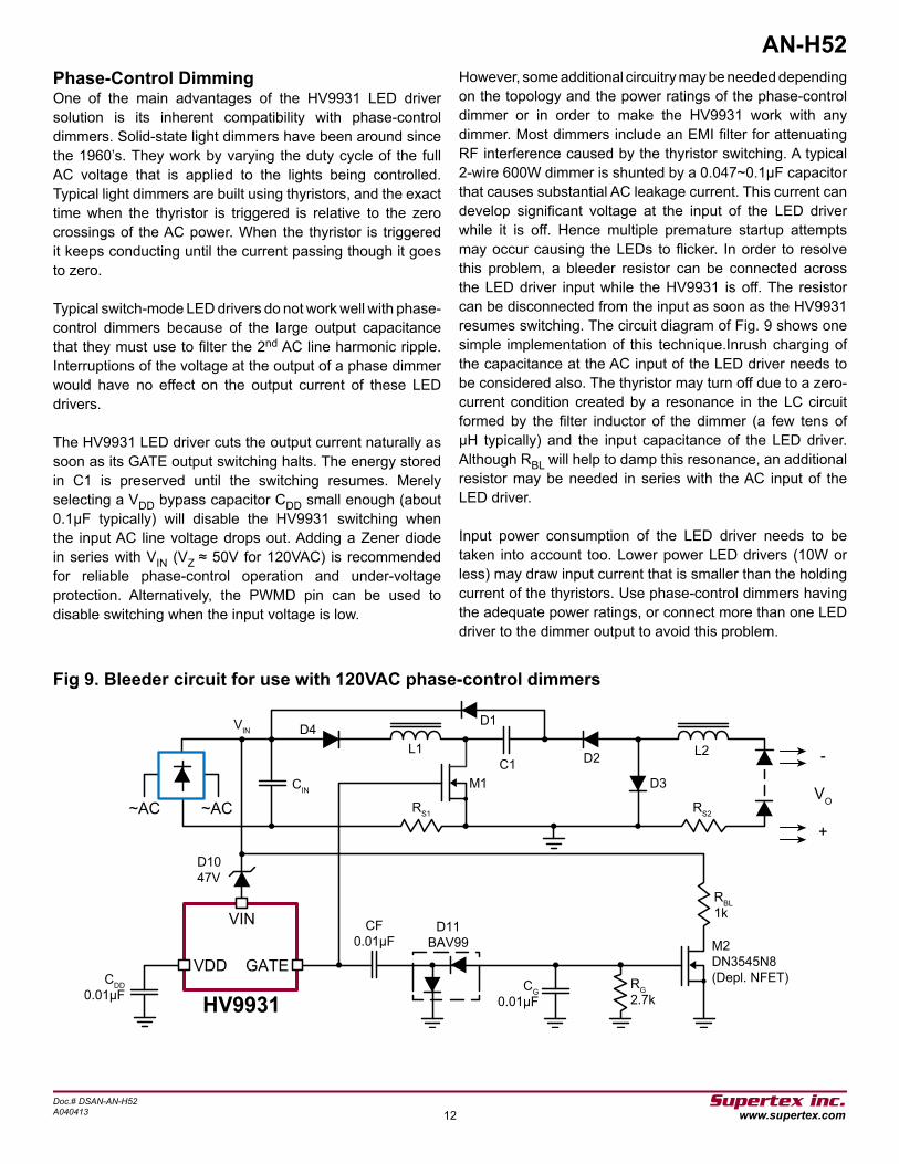
The HV9931 LED driver cuts the output current naturally as soon as its GATE output switching halts. The energy stored in C1 is preserved until the switching resumes. Merely selecting a VDD bypass capacitor CDD small enough (about 0.1µF typically) will disable the HV9931 switching when the input AC line voltage drops out. Adding a Zener diode in series with VIN (VZ ≈ 50V for 120VAC) is recommended for reliable phase-control operation and under-voltage protection. Alternatively, the PWMD pin can be used to disable switching when the input voltage is low.
However, some additional circuitry may be needed depending on the topology and the power ratings of the phase-control dimmer or in order to make the HV9931 work with any dimmer. Most dimmers include an EMI filter for attenuating RF interference caused by the thyristor switching. A typical 2-wire 600W dimmer is shunted by a 0.047~0.1µF capacitor that causes substantial AC leakage current. This current can develop significant voltage at the input of the LED driver while it is off. Hence multiple premature startup attempts may occur causing the LEDs to flicker. In order to resolve this problem, a bleeder resistor can be connected across the LED driver input while the HV9931 is off. The resistor can be disconnected from the input as soon as the HV9931 resumes switching. The circuit diagram of Fig. 9 shows one simple implementation of this technique.Inrush charging of the capacitance at the AC input of the LED driver needs to be considered also. The thyristor may turn off due to a zero-current condition created by a resonance in the LC circuit formed by the filter inductor of the dimmer (a few tens of µH typically) and the input capacitance of the LED driver. Although RBL will help to damp this resonance, an additional resistor may be needed in series with the AC input of the LED driver.
Input power consumption of the LED driver needs to be taken into account too. Lower power LED drivers (10W or less) may draw input current that is smaller than the holding current of the thyristors. Use phase-control dimmers having the adequate power ratings, or connect more than one LED driver to the dimmer output to avoid this problem.
Fig 9. Bleeder circuit for use with 120VAC phase-control dimmers
VIN
GATE
VIN
L1 L2C1
M1 D3
RS1 RS2
D4
-
VO
+
D1
D2
~ACCIN
CG0.01µF
RG2.7k
D11BAV99
CF0.01µF
D1047V
VDDM2DN3545N8(Depl. NFET)
RBL1k
HV9931
~AC
CDD0.01µF

13Supertex inc.
www.supertex.comDoc.# DSAN-AN-H52A040413
AN-H52Output Open Circuit And Input Under Voltage ProtectionHV9931 is a constant output current source. Hence it can generate destructive voltage at its output in the case of an output open circuit condition. A simple circuit shown in Fig. 10 protects the HV9931 LED driver from the output over-voltage. Zener voltage of D12 greater than the maximum output voltage must be selected. Resistor ROV is typically 100~200Ω. However, it still may affects the output current divider ratio and needs to be included in the calculations by replacing RCS2 by (RCS2 + ROV) in the equation (3). Note, that the open circuit can create an over-voltage condition across C1. This voltage stress can be limited by connecting a Zener diode or TVS across C1 limiting the voltage to some acceptable level greater than VC(max). The power dissipation in this voltage clamp device is usually small, since the HV9931 operates at minimum duty cycle during the open circuit condition.
The HV9931 inherently protects the LED driver from an input under voltage condition by limiting the input current. However, increased input current may generate excessive power dissipation in L1, D4, M1 and RCS1. Additional protection is recommended by connecting a Zener diode in series with the VIN pin of the HV9931. (See D10 in Fig. 9)
In addition to D10, an improved input under voltage protection circuit is shown in Fig.10a that can achieve better performance compared to the simple fixed input current limiting. The reference for the CS1 comparator is derived from the input rectified AC waveform. The voltage divider ratio of R1 :RREF1 is programmed such that the Zener diode ZREF1 clamps the divider voltage at any input greater than VAC(min), i.e.:
R1 = RREF1 • VAC(MIN) • √2 - VZREF1 (41)
VZREF1 VREF = VZREF1 should be used with the equation (3) to set the peak current limit for L1 within the normal operating input AC voltage range. When the input voltage falls below VAC(min), the reference voltage will reduce too preventing the inductor L1 from entering continuous conduction mode (CCM). (Operating L1 in CCM can cause undesirable LED flickering, audible noise and excessive heat dissipation due to the loop oscillation.) RBIAS creates a positive offset voltage to maintain the reference above 0V in the zero crossings of the AC line voltage, and thereby prevents interruptions of the output current.
Fig 10a. Input under voltage protection
Fig 10. Output open circuit protection
VDD
CS1
RBIAS
RREF1
AC Bridge “+”
R1
D10
RCS1
to RS1 “-”
VZREF1VIN
HV9931 ZREF1
VDD
CS2
RREF2
RCS2
D12
ROV
to -VO
HV9931
VZ > VO
to +VO

14Supertex inc.
www.supertex.comDoc.# DSAN-AN-H52A040413
AN-H52
VDD
PWMD
HV9931
ZD15.6V
to CIN “+”
MOV1430V
100k
MMBT2222A
10k2.7k
VIN
HV surge
2.7k
Fig 11. Transient voltage protection.
Surge Immunity and EMI ConsiderationsHigh voltage surges occur on the AC power mains as a result of switching operations in the power grid and from nearby lightning strikes. LED lighting and signal equipment may be subjected to surge immunity compliance testing in accordance with various standards (EN61000-4-5, NEMA TS-2 2.1.8 etc.) to insure its continued reliable operation if subjected to realistic levels of surge voltages. The HV9931 LED driver circuit relies mainly on the transient suppressors (MOV, TVS) to protect it from the input AC line surge. There is little capacitance available at the AC input of the LED driver to absorb high surge energy. Thus a transient suppressor needs to be connected across the AC input terminals.
Additional protection circuitry may be also required to protect M1, D1, D2 and the HV9931 itself. A simple circuit shown in Fig.11 clamps the voltage at VIN in the case of an input over-voltage transient. At the same time, it disables the GATE output of the HV9931 to protect the switching components. When HV9931 is disabled, M1 and D1 will only have to withstand the input surge voltage VSURGE rather than (VSURGE + VC ).
As with all switching converters, selection of the input filter is critical to obtaining good EMI. The HV9931 solution provides an inherent advantage of the frequency dither due to the AC voltage ripple across C1 when the fixed off-time operating mode is used. The C1 voltage feedback introduces additional frequency dither when utilized. Hence the required noise attenuation can be lowered yielding a smaller EMI filter.
Some important guidelines must be followed for optimal EMI performance of the HV9931 power converter. The area of the fast switching loops shown in Fig.11 must be
minimized. The first loop including of M1, C1, D2 and D3 can significantly degrade the overall EMI performance due to the reverse recovery current in D3. Using soft recovery diode is recommended for D3. Adding an RC snubber circuit across D3 can be useful (not shown in Fig.11). The second loop consists of CIN, D1, C1, M1 and RS1. Since the input buck-boost stage runs in DCM, the reverse recovery current in D1 is insignificant. However, charging its junction capacitance can generate fast current transients. The large physical dimensions of C1 can complicate optimal routing of these loops. Auxiliary low ESR/ESL capacitors Caux1 and Caux2 can be used for optimizing the printed circuit board routing. Caux1 and Caux2 are responsible for the fast switching transition currents only and hence are typically very small. When these bypass capacitors are used, the areas formed by Caux1, D1, Caux2, M1, RS1 and M1, Caux2, D2, D3 need to be considered mainly.
Optimal routing of the HV9931 gate output loop can be important for EMI performance as well as for preventing destructive oscillations of the M1 gate voltage. The gate driver loop area must be minimized. The trace connecting the source terminal of M1 with the GND pin of the HV9931 must be as short as possible. The VDD bypass capacitor CDD must have low ESR and needs to be placed in the immediate proximity of the HV9931.
Post-conduction oscillation across D4 during the dead time of L1 can be another substantial source of RF emission. Adding a snubber circuit (Rd and Cd in Fig.11) can help significantly. In addition, this snubber is needed to reduce the voltage stress at D4 as it has been discussed in the previous sections.

15Supertex inc.
www.supertex.comDoc.# DSAN-AN-H52A040413
AN-H52
GND
GATE
VO
+
-
~AC
VDD
HV9931
~AC M1
D2 C1
CAUX2 D1 L1 D4 VIN
CD
RD
CIN CAUX1
RS1 RS2
D3
CDD
L2
DDDD
CC 2 2
MM
D2D2
Fig 12. Fast switching current loops.
LED DRIVER DESIGN EXAMPLELet us design a power converter for driving LEDs with the following characteristics:
Input AC Line Voltage 80 - 260VAC, 50-60HzOutput Current 750mAOutput Current Ripple ±15%Output Voltage 25V (max.)THD <20% at 120VACOFF Time 10µsPredicted Efficiency 76%
We will assume that the efficiencies of the input buck-boost stage and the output buck stage are η1 = 0.85 and η2 = 0.9 correspondingly. The efficiency of a DCM buck-boost stage is typically lower compared to the CCM buck stage. The overall efficiency η = η1η 2 ≈ 0.76.
Step 1. Using the equation (2), we will calculate the timing resistor RT value for TOFF = 10µs. The resulting timing resistor: RT = 228K.
Step 2. We will allow 30% peak-to-peak switching current ripple in L2, or ∆iL2 = 0.3iL2 = 0.225A. Then according to the equation (4), the peak current in L2 is:
iL2(PK) = 0.86A.
The value of L2 can be calculated from the equation (28).
L2 ≈ 1.2mH
The DC current rating of L2 equals to IO = 0.75A. The saturation current must satisfy the condition (29) resulting in ISAT > 0.86A.
Step 3. Assuming 0.25W power dissipation in the output current sense resistor RS2, we can calculate its value.
RS2 = 0.25W
≈ 0.44Ω IO
2
We will select a 0.47Ω 1/2W resistor for RS2. Let us use the VDD pin as a reference voltage (VDD = 7.5V).

16Supertex inc.
www.supertex.comDoc.# DSAN-AN-H52A040413
AN-H52(Note, that although VDD is relatively precise, it may exhibit certain dropouts near the AC line voltage cusps when there is no input voltage available at VIN. An external voltage reference is needed for better accuracy.) Selecting RREF2 = 100K, we can calculate the value of RCS2 using the equation (3). R CS2 = 5.4KΩ
Step 4. The input inductor L1 is assumed to reach boundary conduction mode (BCM) at VAC(MIN) at the peak of the input voltage hump. Using the equation (10), we can calculate the critical inductance value that meets this condition.
L1 = 377µH
Step 5. Let us calculate the parameter δ and the duty cycle D at VAC(MIN), VAC(MAX) and VAC using equations (15) and (16):
1) δmin = 14, Dmax = 0.41 at 80VAC;2) δmax = 146, Dmin = 0.15 at 260VAC;3) δ = 31, D = 0.3 at 120VAC.
Step 6. The maximum peak current in L1 will occur at VAC(min). It can be calculated from the equation (9).
iL1(PK) = 2.1A
Note that most “off-the-shelf” 330µH DC chokes may be not suitable for L1. Since the current in L1 cycles from 0 to as high as iL1(PK) every switching cycle, there may be excessive power dissipated in the magnetic core of L1 due to large magnetic flux excursion. On the other hand, the wire gauge used in such inductors is selected based on its DC current rating, whereas the RMS current in L1 is substantially lower than its peak current. Thus, custom designing of L1 is likely to produce a more size efficient solution.
Step 7. The next step is calculating the input current sense and divider resistors RS1 and RCS1. Let us allow 0.1W of power dissipation in RS1 at VAC(MIN). Power dissipation in RS1 can be calculated as:
WRS1 = DMAX • IL1(PK)
2 • RS1
6
Solving this equation for RS1, we obtain:
RS1 ≈ 0.47Ω
Let us select RS1 0.47Ω 1/4W. To calculate RCS1, we will use the equation (3) assuming VREF = VDD and RREF1 = 100K as before. We will program the peak input current limit as 120% of iL1(PK). Then:
RCS1 = 15.8KΩ
Step 8. Let us assume the third harmonic distortion coefficient K3 = 0.15 at VAC = 120VAC. Then, the equation (23) gives the value of C1.
C1 ≈ 31µF
Using the same equations (18) at VAC = 260VAC, we can calculate the required voltage rating of C1.
VC(MAX) = 182V
The voltage ripple at C1 is small at high input voltage. The equation (22) gives KC(MIN) = 0.032. Thus, the peak voltage at C1 is:
VC(PK) = (1 + KC(MIN)) VC(MAX) = 188V
The switching ripple current rating is calculated using the equations (23a):
IC(sw)(MAX) = 0.82A(rms) at 80VAC, IC(sw) = 0.68A(rms) at 120VAC.
The 120Hz ripple current rating is calculated using the equations (23b):
IC(LINE)(MAX) = 0.22A(rms) at 80VAC, IC(LINE) = 0.16A(rms) at 120VAC.
An electrolytic capacitor 33uF,200V can be selected for C1.

17Supertex inc.
www.supertex.comDoc.# DSAN-AN-H52A040413
AN-H52Step 9. If a smaller film capacitor is desired for C1, the circuit of Figure 6 can be used. The value of RFF is calculated at VAC = VAC(MAX) = 260VAC and VO = VO(MAX) = 25V using the equation (26).
RFF = 3MΩ
Select RFF 3.3MΩ to avoid loop oscillation at high AC line voltage. CFF is selected such that:
CFF >> 1
2π • RFF • 100Hz
Select CFF 4.7nF, 200V. The minimum value of C1 is limited by (27). Calculation of the C1 value needed to meet the desired harmonic distortion of IAC is very complex. The designer may want to experiment with different capacitance values of C1 to find the optimal one. Experimental verification shows, however, that THD<20% at 120VAC is possible with less than 1/3 of the C1 value calculated above. Two 4.7uF 250V metalized polyester film capacitors connected in parallel were used.
The RB value is selected based on the desired power dissipation such that RB << RFF. A 330K resistor will dissipate 0.1W at VC(max) = 182V. The value of CB is calculated from:
CB >> 1
≈ 4.0nF 2π • RB • 120Hz
The flying capacitor CA must be selected such that:
CA >> TOFF
≈ 25pF RB
We can select CB = CA = 4700pF for simplicity. Both capacitors must be rated to withstand VC(pk). Zener diodes D8 and D9 must not distort the AC ripple waveform at the output of CFF. In other words, their breakdown voltage must be set higher than the C1 voltage ripple amplitude at 120VAC. Leaving D8 and D9 out or selecting the diodes with excessively high breakdown voltage may increase the start-up time of the LED driver.
Step 10. Optimal selecting of the switching MOSFET M1 is based on finding a good balance between the total gate charge Qg and the on-resistance RDS(ON). The drain voltage rating is given by the equation (31).
VDS(max) = 556V
Acceptable Qg is limited by the allowed power dissipation in the HV9931. The power dissipation can be estimated as:
where VZ is Zener voltage of D10.
Let us select SPP03N60C3 for M1. This is a 650V, 3.2A MOSFET by Infineon Technologies with RDS(ON) = 1.26Ω and Qg(max) ≈ 13nC at VDS = 420V, VGS = 7.5V.
Then: WREG(MAX) ≈ 400mW(MAX)
The maximum RMS current in M1 is calculated from the equation (30) as ID(M1) = 0.73A. The peak current in M1 is IL1(PK)+IL2(PK) ≈ 3A. (Note that the maximum power dissipation in HV9931LG (SO-8) must be derated 6.3mW/°C above 25°C. Thus, the maximum operating ambient temperature needs to be less than 60°C. Using HV9931P (DIP-8) will be limited to TA < 80°C.) A larger VZ can be selected to reduce power dissipation in the HV9931.
Step 11. In accordance with the equations (32)-(35), the average currents in D1-D4 are:
ID1 = 0.33A, ID2 = 0.31A, ID3 = 0.64A, ID4 = 0.6A.
Peak currents in D1 and D4 equal to the peak current in L1 or: I D1(PK) = I D4(PK) = IL1(PK) = 2.1A.
WREG(max) = 2√2
• VAC(max) - VZ π
• Qg • (1 - Dmin ) VREF +
TOFF
VREF
RREF1 RREF2
+ + 1mA

Supertex inc. does not recommend the use of its products in life support applications, and will not knowingly sell them for use in such applications unless it receivesan adequate “product liability indemnification insurance agreement.” Supertex inc. does not assume responsibility for use of devices described, and limits its liabilityto the replacement of the devices determined defective due to workmanship. No responsibility is assumed for possible omissions and inaccuracies. Circuitry andspecifications are subject to change without notice. For the latest product specifications refer to the Supertex inc. (website: http//www.supertex.com)
©2013 Supertex inc. All rights reserved. Unauthorized use or reproduction is prohibited. Supertex inc.1235 Bordeaux Drive, Sunnyvale, CA 94089
Tel: 408-222-8888www.supertex.com18
AN-H52
Doc.# DSAN-AN-H52A040413
The equations (36)-(38) give the reverse voltage across D1-D3, resulting in:
VR(D1) = 562V, VR(D2) = 368V, VR(D3) = 188V.
Adding an RC snubber is recommended across D4. Reverse voltage across D4 depends on the capacitance value of CDselected for this RC snubber. The snubber capacitor CDd needs to be greater than COSS+ Cj1, where COSS is drain-to-source capacitance of M1, and Cj1 is the reverse biased junction capacitance of D1. Usually, Cj1 can be disregarded compared to the COSS. The typical data by Infineon shows COSS < 20pF at VDS > 100V for SPP03N60C3. BYD57K by Philips (800V,1A, trr = 75ns) can be selected for D1. The
BYD57K data by Philips shows Cj < 2pF at VR > 100V. By choosing Cd = 200pF and Rd = 2.7KΩ, we can use a 400V rectifier for D4, for example, BYD57G (400V, 1A, trr = 30ns) by Philips.
Fast switching rectifiers are needed for D2 and D3. We can select D2 STTA106A (600V, 1.0A, trr = 20ns) and D3 STTH102A (200V, 1.0A, trr = 30ns) by STMicroelectronics.
Step 12. Output filter capacitor CO of a few hundred nanofarads will be needed for improved EMI performance. Alternatively, a larger value of this capacitor can be used to reduce the switching ripple current in the LEDs further.