Embed Size (px)
Citation preview
Low-Power Transmitter Based on
Data Transition Information
Sung-Geun Kim
The Graduate School
Yonsei University
Department of Electrical and Electronic Engineering

Low-Power Transmitter Based on
Data Transition Information
by
Sung-Geun Kim
A Dissertation
Submitted to the Department of Electrical and Electronic Engineering
and the Graduate School of Yonsei University
in partial fulfillment of the requirements for the degree of
Doctor of Philosophy
August 2017

This certifies that the dissertation of Sung-Geun Kim is approved.
________________________________
Thesis Supervisor: Woo-Young Choi
________________________________
Seong-Ook Jung
________________________________
Tae Wook Kim
________________________________
Kangyeob Park
________________________________
Young-Seok Park
The Graduate School
Yonsei University
August 2017

i
Table of Contents
Table of Contents ............................................................................... i
List of Tables ..................................................................................... iv
List of Figures ................................................................................... vi
Abstract ........................................................................................... xiv
1. Introduction .................................................................................... 1
1.1. High-Speed Low-Power Serial Interface ................................ 1
1.2. Power Dissipation in Transmitter ........................................... 9
1.3. Outline of Dissertation .......................................................... 12
2. Transmitter Based on Data Transition Information ................. 13
2.1. Data Transition Information in Serialized Data ................... 13
2.2. Extracting Data Transition Information and Serializing with
Toggle Signals .............................................................................. 18
2.3. Pre-Emphasis with Toggle Signals ....................................... 29

ii
3. Circuit Implementation ............................................................... 31
3.1. Quadrature Clock Generation ............................................... 33
3.2. DFF and Toggle to NRZ ....................................................... 35
3.3. Voltage-Mode Output Diver with Pre-Emphasis ................. 41
3.4. Power Consumption Comparison ......................................... 49
4. Measurement Results ................................................................... 60
4.1. Chip Fabrication and Measurement Setup ............................ 60
4.2. Eye Diagram and Energy Efficiency .................................... 63
4.3. Summary ............................................................................... 72
5. Application Extension .................................................................. 73
5.1. Duobinary with Toggle Signals ............................................ 77
5.1.1. Relationship between Duobinary and Toggle Signals
................................................................................................ 77
5.1.2. Voltage-Mode Duobinary Output Driver with Toggle
Signals .................................................................................. 79
5.1.3. Duobinary Receiver with 1-Tap DFE ......................... 86
5.1.4. Implementation and Measurement Results ................. 90
5.2. Duobinary with Consecutive Signals ................................... 98
5.2.1. Relationship between Duobinary and Consecutive
Signals .................................................................................. 98
5.2.2. Consecutive Signal Generation ................................. 100

iii
5.2.3. Voltage-Mode Duobinary Output Driver with
Consecutive Signals ............................................................ 104
5.2.4. Phase Calibration with Toggle Signals ..................... 110
5.2.5. Implementation and Measurement Results ............... 117
6. Conclusion ................................................................................... 124
Bibliography .................................................................................. 126
List of Publications ....................................................................... 129

iv
List of Tables
Table. 2-1. Truth table between serialized data and toggle signals.... 27
Table. 3-1. Dynamic power consumption analysis of conventional
transmitter ...................................................................... 54
Table. 3-2. Dynamic power consumption analysis of our transmitter
with toggling serializer .................................................. 56
Table. 4-1. Detailed performance summary and comparison .......... 71
Table. 5-1. Relationship among serialized signal, toggle signals, and
duobinary signal ............................................................ 78
Table. 5-2. Truth table for duobinary driver .................................... 82
Table. 5-3. Performance summary of duobinary transmitter ........... 97
Table. 5-4. Performance summary of duobinary receiver ................ 97
Table. 5-5. Relationship among consecutive signal, and duobinary
signal .............................................................................. 99

v
Table. 5-6. Truth table for duobinary driver .................................. 107
Table. 5-7. Performance summary of duobinary transmitter ......... 123
vi
List of Figures
Fig. 1-1. Typical serial interface block diagram. .................................. 3
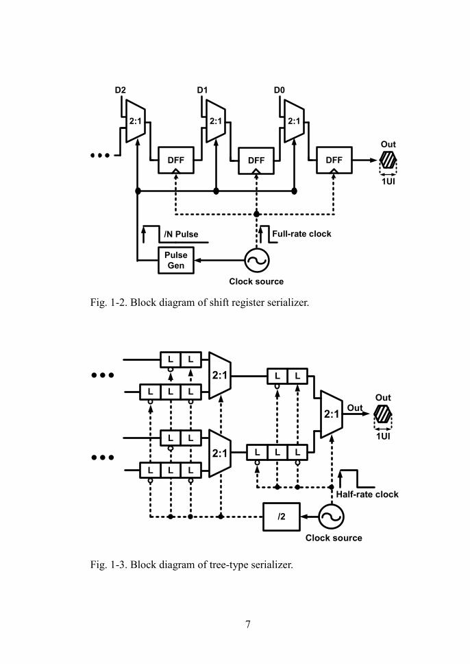
Fig. 1-2. Block diagram of shift register serializer. .............................. 7
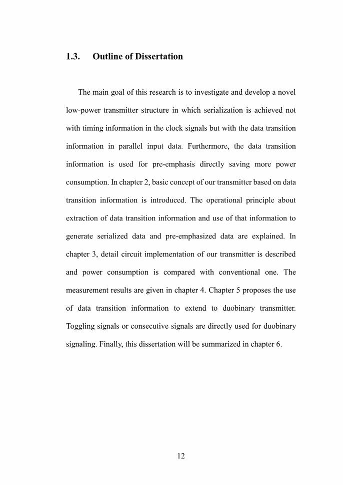
Fig. 1-3. Block diagram of tree-type serializer. .................................... 7
Fig. 1-4. Block diagram of large ratio serializer. .................................. 8
Fig. 1-5. Block diagram of 4:1 ratio transmitter. ................................ 11
Fig. 2-1. Block diagram of large ratio serializer. ................................ 15
Fig. 2-2. Timing diagram of conventional 4:1 serialization and toggle
signals. ............................................................................................... 16
Fig. 2-3. Timing diagram of conventional 4:1 serialization and toggle.
............................................................................................. 17
Fig. 2-4. (a) Conventional serialization block and (b) data transition
extraction block. .................................................................................. 24

vii
Fig. 2-5. Data transition extraction and toggle signals. ...................... 25
Fig. 2-6. Timing diagram and block diagram for RZ converting. ...... 26
Fig. 2-7. Timing diagram for serialized data generation from toggle. 27
Fig. 2-8. Overall block and timing diagram of toggling serializer. .... 28
Fig. 2-9. Pre-emphasis with toggle signals. ........................................ 30
Fig. 3-1. Block diagram of total transmitter. ...................................... 32
Fig. 3-2. PPF and DCC for quadrature clock generation. ................... 34
Fig. 3-3. Simulation results of phase distortion of PPF as operation
frequency and phase compensation range of DCC. ............................ 34
Fig. 3-4. (a) Timing diagram for RZ generation, and (b) TSPC DFF used.
............................................................................................... 38
Fig. 3-5. (a) NOR gate based SR-Latch, and (b) push-pull SR-Latch.
............................................................................................. 39

viii
Fig. 3-6. Simulation results of (a) conventional SR-Latch, and (b) push-
pull SR-Latch. ..................................................................................... 40
Fig. 3-7. Schematic of VMDRV (a), VMDRV operation with high SP
and low SN state, and VMDRV operation with high SN and low SP state.
............................................................................................... 45
Fig. 3-8. Schematic of VMDRV with pre-emphasis. .......................... 46
Fig. 3-9. Regulator and replica circuit for impedance matching. ....... 47
Fig. 3-10. Regulator and replica circuit for pre-emphasis and boosting
gain control. ........................................................................................ 48
Fig. 3-11. Block diagram for power comparison simulation: (a)
conventional transmitter, (b) transmitter with toggling serializer. ...... 52
Fig. 3-12. Detail block diagram of conventional transmitter used for
power consumption analysis. .............................................................. 53
Fig. 3-13. Detail block diagram of our transmitter with toggling serializer
used for power consumption analysis. ................................................ 55
Fig. 3-14. Simulated power consumption of conventional and our

ix
proposed transmitter at 8 Gb/s in 65nm CMOS, respectively. ........... 57
Fig. 3-15. Transient noise simulation with 1 % supply noise at 5 and 8
Gb/s. ............................................................................................... 58
Fig. 3-16. Simulated jitter increase with supply noise at various data rate.
............................................................................................... 59
Fig. 4-1. Chip microphotograph of our transmitter. ........................... 61
Fig. 4-2. Measurement setup. ............................................................. 62
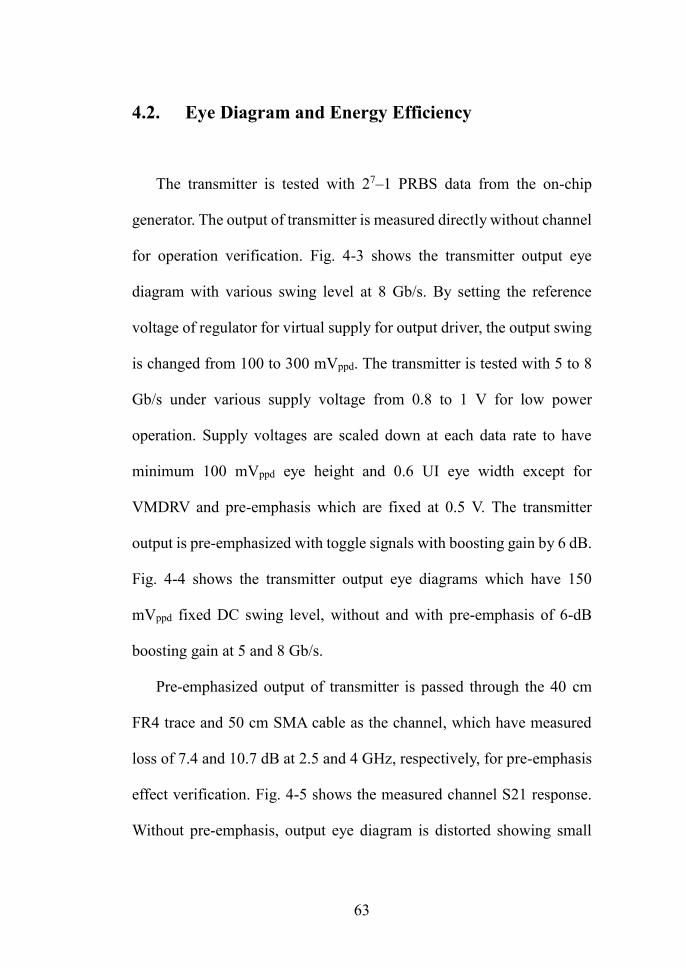
Fig. 4-3. Measured transmitter output eye diagram with various swing
level. ............................................................................................... 66
Fig. 4-4. Measured transmitter output eye diagram with and without pre-
emphasis at 5 and 8 Gb/s having 150mVppd output DC swing. ............ 67
Fig. 4-5. Measured channel S21 response. ......................................... 68
Fig. 4-6. Measured channel output eye diagram with and without pre-
emphasis at 5 and 8 Gb/s. ................................................................... 69

x
Fig. 4-7. Measured energy efficiency and comparison. ...................... 70
Fig. 5-1. (a) Linear model of duobinary signaling. (b) Composition of
duobinary spectrum. ............................................................................ 75
Fig. 5-2. Output spectra and waveforms for different data formats
passing through an ideal filter. (a) NRZ. (b) Duobinary. .................... 76
Fig. 5-3. Timing diagram of serialized signal, toggle signals, and
duobinary signal. ................................................................................. 78
Fig. 5-4. Equivalent resistance model of duobinary voltage mode output
driver and voltage level of ‘two’ and ‘zero’ level case (a), and ‘one’ level
case (b). ............................................................................................... 81
Fig. 5-5. Voltage-mode duobinary output driver with toggle signal. .. 82
Fig. 5-6. Inverter based XNOR gate (a), and use of XNOR gate as
inverter buffer (b). ............................................................................... 83
Fig. 5-7. Voltage-mode duobinary output driver with replica bias circuits
for duobinary ‘one’ level. .................................................................... 84
Fig. 5-8. Voltage-mode duobinary output driver with replica bias circuit

xi
for duobinary ‘two’ and ‘zero’ level. .................................................. 85
Fig. 5-9. The concept of duobinary-to-NRZ converter. ...................... 88
Fig. 5-10. Timing diagram of duobinary-to-NRZ converter. .............. 88
Fig. 5-11. Differential duobinary-to-NRZ converter. ......................... 89
Fig. 5-12. Chip microphotograph. (a) Duobinary transmitter, (b)
duobinary receiver. .............................................................................. 92
Fig. 5-13. Measurement setup. ........................................................... 93
Fig. 5-14. Measured duobinary transmitter output eye diagram at 5 Gb/s
(a), and 8 Gb/s (b). .............................................................................. 94
Fig. 5-15. Simulated PRBS pattern and duobinary pattern from 27–1
PRBS pattern and measured duobinary pattern. ................................. 95
Fig. 5-16. Measured duobinary receiver output eye diagram at 2
Gb/s. ............................................................................................... 96
Fig. 5-17. Measured Bathtub curve of duobinary receiver output at 2Gb/s.

xii
............................................................................................... 96
Fig. 5-18. Timing diagram of serialized signal, consecutive signals, and
duobinary signal. ................................................................................. 99
Fig. 5-19. Consecutive signal extraction. ......................................... 102
Fig. 5-20. Overall block diagram of consecutive serializer. ............. 103
Fig. 5-21. Equivalent resistance model of duobinary voltage mode output
driver and voltage level of ‘two’ and ‘zero’ level case (a), and ‘one’ level
case (b). ............................................................................................. 106
Fig. 5-22. Voltage-mode duobinary output driver with consecutive signal.
............................................................................................. 107
Fig. 5-23. Voltage-mode duobinary output driver with replica bias
circuits for duobinary ‘two’ or ‘zero’ level. ...................................... 108
Fig. 5-24. Voltage-mode duobinary output driver with replica bias
circuits for duobinary ‘one’ level. ..................................................... 109
Fig. 5-25. Training toggle signal sequence for differential (a) and
quadrature phase calibration (b). ....................................................... 112

xiii
Fig. 5-26. Block diagram of differential phase calibration. .............. 113
Fig. 5-27. Block diagram of quadrature phase calibration. .............. 114
Fig. 5-28. Phase decision circuit. ...................................................... 115
Fig. 5-29. Simulation results of phase calibration block. ................. 116
Fig. 5-30. Block diagram of duobinary transmitter with consecutive
signals. ............................................................................................ 119
Fig. 5-31. Chip microphotograph. .................................................... 120
Fig. 5-32. Measured duobinary transmitter output eye diagram at 12.5,
20, and 25 Gb/s. ................................................................................ 121
Fig. 5-33. Measured duobinary transmitter output eye diagram with and
without phase calibration at 20 and 25 Gb/s. .................................... 122
xiv
Abstract
Low-Power Transmitter Based on
Data Transition Information
Sung-Geun Kim
Dept. of Electrical and Electronic Engineering
The Graduate School
Yonsei University
Due to the demand of high quality multi-media data is increased, the
amount of data traffic for all kinds of data stream is increased. High-
speed serial interface is the most effective way to deal with this increased
data amount. In addition to the high-speed operation, energy efficiency
become more important in serial interface, with the increased use of
portable device. As the transmitter is most power hungry block in serial
interface, the lower power transmitter is issued now days.
In this dissertation we demonstrate a low-power wireline transmitter

xv
in which serialization is achieved by toggling serializer with data
transition information extracted from parallel input data. This novel
technique of serialization provides significantly reduced power
consumption since it does not need the short pulse generation block
required in the conventional serializer. In addition, the same data
transition information can be directly used for implementing 2-tap pre-
emphasize and, consequently, the need for the additional serializer
required in the conventional pre-emphasis circuits can be eliminated,
resulting in further reduced power consumption. A prototype transmitter
realized in 65nm CMOS technology achieves energy efficiencies of
0.202 pJ/bit at 5 Gb/s and 0.3 pJ/bit at 8 Gb/s for 150 mVpp,d output
voltage swing without preemphasis, and 0.252 pJ/bit at 5 Gb/s and 0.333
pJ/bit at 8 Gb/s with 2-tap pre-emphasis providing 6-dB equalization
gain.
We extended our transmitter with data transition information to
duobinary transmitter. Due to the inherent characteristic of duobinary
generation which use data transition information of adjacent serialized
data, toggle signal extracted from our toggling serializer can be directly
used with impedance modulation voltage-mode duobinary output driver.
Duobinary transmitter with toggle signals and receiver are realized in
65nm CMOS technology. Duobinary signal generation with toggle

xvi
signal and transmission are successfully demonstrated with 27–1 PRBS
data at 5 to 8 Gb/s. Transmitted duobinary data received and converted
to NRZ data with 1-tap DFE receiver. BER and Bathtub measurement of
receiver verifies the operation of receiver with duobinary to NRZ
conversion. To reduce the complexity of voltage-mode duobinary output
driver, consecutive signals are generated and used for duobinary
generation instead of toggle signals. With consecutive signals, toggle to
NRZ converter can be eliminated using same structure in serializer for
generation of consecutive signals except for the connection of parallel
input data. Quadrature and differential phase calibration block are added
for clear serialization using toggle signals which re-use the consecutive
signal generator. Duobinary transmitter with consecutive signal is
realized in 28nm CMOS technology. Duobinary signal generation with
consecutive signal is successfully demonstrated with 27–1 PRBS data at
12.5 to 25 Gb/s and operation of phase calibration block is verified with
eye diagram measurement.
Keywords: transmitter, low power transmitter, energy efficient, pre-
emphasis, data transition information, toggling serializer, consecutive
serializer, phase calibration

1
1. Introduction
1.1. High-Speed Low-Power Serial Interface
As the need of high quality multi-media data is increased, the amount
of data for internet networking, server networking, display interface and
so on become increased, which deal with all kinds of data stream. To
transmit this massive data, two interface method can be used: parallel
interface or serial interface. In the parallel interface, each data stream is
transmitted through each channel. Although this parallel method is easily
implemented, the number of I/O pin is increased as many as the increased
transmission speed. This results in the increasing package cost seriously
due to the large area and number of pins. In addition, parallel method
inherently have some problems such as data skew, clock skew and
crosstalk.
These problems mentioned in the parallel interface can be solved
with serial interface. In serial interface, all the parallel data streams for
massive data are combined in one serial data stream, and this serial data
stream is transmitted by single channel. For this reason, serial interface
is widely used in modern high-speed communication such as PCI
(peripheral component interconnect) express, Ethernet, USB (universal

2
serial bus), serial ATA (advanced technology attachment), HDMI (high-
definition multimedia interface), DVI (digital visual interface), and
DisplayPort.
To use the serial interface method, serializer and deserializer which
combines the parallel data to serial data and splits serial data into parallel
data are necessary in the transmitter and receiver, respectively. Fig. 1-1
shows a typical block diagram of a serial interface with channel. A
serializer/deserializer is simply called SERDES. The transmitter receives
low speed parallel data from a source digital core and combines it in
serializer with clock generated from clock source. The serialization is
performed by multiplexer which should be synchronized with a clock.
The serialized data finally are transmitted with output driver, which can
be implemented in various type according to the detail application
specification. The transmitted serialized data stream passes through a
channel and are received in the front-end of receiver which is generally
implemented with sampler. Received serial data stream is converted to
the parallel data with deserializer incorporated de-multiplexer. A clock
for the de-multiplexer also should be synchronized with the system clock
in transmitter, but if any additional clocking information is not
transmitted from the transmitter, the receiver should recover the clock
from the received data stream. This operation is performed clock-and-

3
Serializer
Ou
tpu
t
Dri
ver
ΔT
a1
Pre
-dri
ver
Pre
-em
ph
as
is
TX
Data
De-
Serializer
Clo
ck/D
ata
Re
co
very
Eq
ua
lizer
TX
Data
Channel
Da
ta
RX
Data
Clo
ck S
ou
rce
Fig. 1-1. Typical serial interface block diagram.

4
data-recovery (CDR) circuit. For compensation of low-pass filtering
characteristic of the channel, pre-emphasis and equalizer are employed
in transmitter and receiver, respectively.
Dealing with the massive data, transmission speed become higher in
serial interface and energy efficiency become more important issue now
days in some application such as mobile devices in which battery life
time is important or data center in which hundreds of thousands of
servers using serial interface to communicate each other are concentrated
in one place. In serial interface, transmitter is most power hungry block
which deals with fastest data stream and reducing transmitter power
consumption is very important for reducing total serial interface power
consumption. Most of power consumed in transmitter are two part. One
is the serialization with clocking and the other is output driver with pre-
emphasis.
In first, several types of serializer have been developed for low power
design: shift register [1], tree-type [2], and large ratio multiplexer [3].
Fig. 1-2 shows the operation of shift register. 2:1 multiplexer receives
one of parallel data and output data of before multiplexer, combines
those data with short pulse, and delivers multiplexed data to the DFF.
The DFF moves 1-bit with full-rate clock whose period is equal to that
of the final serialized data. Though this method is straightforward,

5
multiplexers and DFFs needs high-speed short pulse and full-rate clock
consuming large power. Also, the maximum operating data rate is limited
by device performance. Tree-type serializer consists of 2:1 multiplexers
with five latches for data aligning to avoid glitch problem as shown in
Fig. 1-3. Each stage of multiplexers operates with clock which have same
period of input data rate of each multiplexer. Thus, final stage of
serializer uses half-rate clock and remaining parts of serializer use lower
speed clock, leading to save power consumption. Even though the tree-
type serializer use lower speed clock than shift register type serializer, it
use half-rate clock in final stage consuming large power. Large ratio
serializer uses large fan-in multiplexer which serializes more than two
input data by pulse signals generated from multi-phase clock signals as
shown in Fig. 1-4. The clock speed can be lower with the ratio of
serializer, but the number of multi-phase of clock is increased also. In
addition, consideration of parasitic capacitance at the output node of
large fan-in multiplexer is needed for target operation speed.
In second, power consumption of output driver. Static power
consumption of output driver is determined with output swing due to the
channel and receiver impedance matching and this power has large
portion in total power consumption of transmitter. It is well-known that
using voltage-mode output driver is efficient for power saving and one
6
fourth of power can be saved using differential voltage mode output
driver compared to the differential current mode output driver [4].
However, implementing pre-emphasis with voltage-mode output driver
is difficult and needs complex circuits for pre-emphasis increasing power
consumption. For lowering power consumption, many techniques are
investigated but the power consumption for delayed data sequence
generation is inhabitable.
In our research, we investigate a new transmitter topology which
have large fan-in structure based serialization and voltage-mode output
driver with pre-emphasis for lowering power consumption. In addition
to the low power transmitter with pre-emphasis, we investigate
duobinary transmitter with voltage-mode duobinary output driver for
low power consumption.
7
DFF DFFDFF
/N Pulse Full-rate clock
2:1 2:1 2:1
D0D1D2
Out
Pulse
Gen
Clock source
1UI
Fig. 1-2. Block diagram of shift register serializer.
2:1
2:1 LL
LL
L
2:1
Out
Half-rate clock
LL
LL
L
LL
LL
L
Out
1UI
/2
Clock source
Fig. 1-3. Block diagram of tree-type serializer.

8
L/N Pulse
D0
D1
D2
D3Retimer
Out
Clock source
Pulse
Gen
Out
1UI
Fig. 1-4. Block diagram of large ratio serializer.

9
1.2. Power Dissipation in Transmitter
As mentioned before, in low-power wireline transmitters, large ratio
serialization has been used so that power consumption due to distribution
of high-frequency clock signals can be reduced. However, the output
capacitance and parasitic capacitance are increased as the ratio of
serialization is increased. Recently, the low-power transmitters
employing large ratio serialization are reported to reduce power
consumption maintaining operation speed as possible [5]-[7]. Fig. 1-5
shows the block diagram of 4:1 ratio transmitter with pre-emphasis,
which consists of data aligner, pulse generator, serializer, additional
serializer for pre-emphasis, pre-driver, output driver with pre-emphasis,
and clock buffers. The data aligner is used for parallel input data aligning
with quad-rate clocks to avoid glitch problem with serialization. The
pulse generator provide short pulses with quad-rate clocks which have
timing information when and what the parallel input data should be
serialized. With the aligned parallel input data and short pulses provided
from pulse generator, serializer generates final serialized output data and
delivers it to the output driver through the pre-driver stage. Additional
serializer is used to 1-bit delayed data generation for pre-emphasis. As
the large ratio serialization, high-frequency clock signals can be replaced

10
to quad-rate clock so that power consumption due to distribution of high-
frequency clock signals can be reduced. However, despite of using quad-
rate clock, the width of each pulses used for providing precise timing
information to the serializer is same as the period of serializer output data.
Generation and distribution of such short pulse signals having
sufficiently fast rising and falling time consume a fair amount of power.
Increasing of the amount of data demands higher bandwidth not only
for the circuit but also for the channel used in data transmission. Widely
used circuit technique for the channel bandwidth enhancement is FFE
(feed-forward equalization) pre-emphasis. In general, for n-tap pre-
emphasis, serialized output need n-bit delay which can be generated with
DFF using full-rate clock. To avoid the use of full-rate clock, additional
n serializers are used for n-bit delayed data using phase shifted short
pulses. In simple case, the channel shows 1-pole low-pass filter
characteristic, 2-tap pre-emphasis which consists of main tap and 1-bit
delayed tap can be used with minimum additional power consumption
for pre-emphasis. However, additional pre-emphasis also needs short
pulses and increasing of the total transmitter power is inevitable.
To sum it up, transmitter consumes much of power to provide timing
information in final serializer or pre-emphasis and power consumption
can be saved effectively with replace the role of the timing information.

11
Serializer
Additional
Serializer
Output
Driver
Pre-
Emphasis
Pulse
Gen
.
Data
Aligner
Clock
Buffers
AB
CD
0
90
180
270
90
180
270
0
AB
CD
AB
CD
0
90
180
270
Pre-
Driver
Pre-
Driver
A
B
C
D
Fig. 1-5. Block diagram of 4:1 ratio transmitter.
12
1.3. Outline of Dissertation
The main goal of this research is to investigate and develop a novel
low-power transmitter structure in which serialization is achieved not
with timing information in the clock signals but with the data transition
information in parallel input data. Furthermore, the data transition
information is used for pre-emphasis directly saving more power
consumption. In chapter 2, basic concept of our transmitter based on data
transition information is introduced. The operational principle about
extraction of data transition information and use of that information to
generate serialized data and pre-emphasized data are explained. In
chapter 3, detail circuit implementation of our transmitter is described
and power consumption is compared with conventional one. The
measurement results are given in chapter 4. Chapter 5 proposes the use
of data transition information to extend to duobinary transmitter.
Toggling signals or consecutive signals are directly used for duobinary
signaling. Finally, this dissertation will be summarized in chapter 6.

13
2. Transmitter Based on Data Transition
Information
2.1. Data Transition Information in Serialized Data
In general 4:1 serialization, parallel data are combined with timing
information which can be provided from quadrature clock signals as
mentioned before. However, if the serializer can combine the parallel
data without timing information from clock signals, much of power
consumed in clock buffers and pulse generators can be saved as shown
in Fig.2-1. Moreover, using the data transition information which is used
for combining parallel data to serial data, output data also can be pre-
emphasized without any clock signals. As the information for pre-
emphasis is generally provided from 1-bit delayed final output data
which deals with highest speed clock signals in the transmitter, plenty of
power can be saved if we pre-emphasis not with the clock signals but the
data transition information.
Before explain about the data transition information, it is helpful to
see the conventional serialization process for understanding the
relationship between data transition information and serialized output
data. Fig. 2-2 shows the timing diagram for conventional 4:1

14
serialization. The aligned parallel data (A, B, C, D) and pulse signals
from quadrature clocks (PA, PB, PC, PD) are combined in serializer. The
pulse signals provide the timing information what and when the parallel
data need to be selected and serialized and parallel data are serialized in
one bit data sequence. In this point, we can see that the serialized output
data consist of two types of information, data transition information and
none transition information. Then we can divide the data transition
information into positive toggle signal, TP, which indicate the data
transition from 0 to 1 and negative toggle signal, TN, which indicate the
data transition from 1 to 0. In other words, if we extract these toggle
signals from parallel input data, we can serialized the output data without
clock.
Fig. 2-3 shows the transmitter with toggling serializer which generate
toggle signals from parallel input data. The aligned parallel input data
are serialized without clock signals in toggling serializer. In addition, the
toggle signals which have data transition information can be used
directly for pre-emphasis without clock saving more power.

15
Ou
tpu
t
Dri
ve
r
Pre
-
Em
ph
asis
Da
ta
Ali
gn
er
Clo
ck
Bu
ffe
rs
AB
CD
Pre
-
Dri
ver
Pre
-D
riv
er
Se
ria
liza
tio
n
wit
ho
ut
Clo
ck
Fig. 2-1. Block diagram of large ratio serializer.

16
T P T N
TN
NN
TT
TN
TT
TT
TT
NT
TT
TT
Output
A B C D
PA
PB
PC
PD
Fig. 2-2. Timing diagram of conventional 4:1 serialization and toggle
signals.

17
Serializer
Output
Driver
Pre-
Emphasis
Data
Aligner
Clock
Buffers
AB
CD
AB
CD
0
90
180
270
Pre-
Driver
Pre-
Driver
A
B
C
D
T P
T N
Fig. 2-3. Timing diagram of conventional 4:1 serialization and toggle
signals.

18
2.2. Extracting Data Transition Information and
Serializing with Toggle Signals
When serialization is performed with timing information from clock
signals, short pulse signals generated from quadrature clocks are
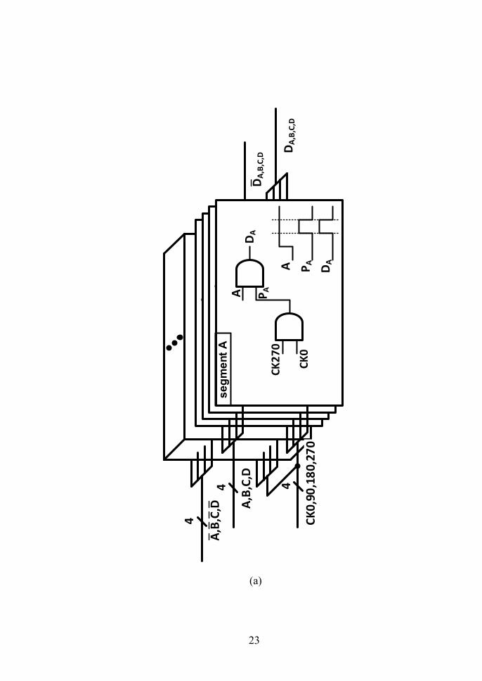
combined with parallel input data. Fig. 2-4 (a) shows the serializer
segment block with parallel input data and clock signals for pulse
generation. One of four parallel input data is selected with pulse signal
generating partial serialized data. For example, parallel input data A is
selected when the pulse signal PA is high in ‘segment A’ block generating
data pulse DA. Other parallel input data B, C, and D are selected with PB,
PC, and PD, respectively, in the same way. Due to the timing information,
each data pulse does not overlap and four parallel input data are
serialized by simple OR operation. However, though serializer uses
quadrature clock lowering clock speed and saving power, short pulses
are needed due to the timing information for not overlapped data pulses.
The blocks for these short pulses consume large power and reduces the
effect of using large ratio serialization for power saving. In order to avoid
using short pulses, serialization is achieved only with the data transition
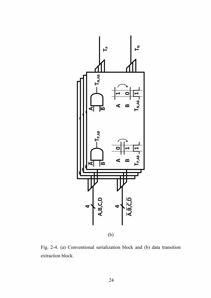
information in our serializer. In Fig. 2-4 (b) shows simply how the data
transition information can be extracted from adjacent parallel input data.
19
When the two adjacent parallel input data compared, the positive
transition information and negative transition information between those
data can be extracted, separately. For example, when the positive
transition is occur between parallel input data A and B, positive transition
information is extracted in positive toggle signal segment, TP,AB, with
simple logic, T𝑃,𝐴𝐵 = A̅&B . When the negative transition is occur,
negative transition information is extracted in negative toggle signal
segment, TN,AB, with simple logic, T𝑁,𝐴𝐵 = A&B̅ . Data transition
information between other parallel input data can be extracted in the
same way generating positive toggle signal and negative toggle signal as
shown in Fig. 2-5. Each four positive toggle signal segments, TP,AB, TP,BC,
TP,CD, TP,DA, are combined by simple OR logic generating final positive
toggle, TP. Negative toggle signal, TN, is generated in the same way.
When the toggle signal segments are combined with OR logic, each
of four segments should not be overlapped as timing diagram shown in
Fig. 2-5. For this we need some operation before data comparison. For
the clear understanding, timing diagram of parallel data is given in Fig.
2-6. The dotted lines show the compared area for extraction of data
transition information. When the adjacent two data are compared, other
two data should not affect to them for extraction of the partial toggle
signals exactly. However, with general aligned parallel input data, it is

20
not. For example, when parallel input data A and B are compared for
extraction of TAB (dotted line), gray colored boxes in data C and D have
other information, disturbing clear extraction just between data A and B.
This prohibit the use of same logic at the same time for all parallel data
comparison. To solve this problem, we can eliminate the gray colored
boxes in the aligned parallel input data when four parallel input data are
aligned as shown in Fig. 2-6. This help clear extraction of data transition
information between adjacent two input data. The parallel input data are
converted to RZ format.
The data transition information in parallel input data is extracted and
saved to the toggle signals. Then, from these toggle signals, serialized
output data can be generated. As mentioned before, positive toggle signal
has positive transition information of serialized output data and negative
toggle signal has negative transition information of serialized output data,
so the serialized output data from toggle signal can be directly made. The
timing diagram for this is shown in Fig. 2-7. When the positive toggle
signal, TP, is high and negative toggle signal, TN, is low, positive output,
SP, is high and negative output, SN, is low. On the contrary, when TP is
low and TN is high, SP is low and SN is high. When both toggle signals,
TP and TN, are low, SP and SN is maintain previous state. Because
serialized data cannot transit both direction at the same time, positive

21
toggle signal and negative toggle signal cannot occur simultaneously.
The truth table which shows the relationship between serialized output
data and toggle signals can be made as shown in Table 2-1. This truth
table indicate that conversion logic for serialized NRZ signals from
toggle signals is just simple SR-Latch. As the inherent characteristic of
toggle signal, forbidden state of SR-Latch never occur.
Overall block diagram and timing diagram of our proposed serializer,
named toggling serializer, is shown in Fig. 2-8. Input parallel NRZ data
(A, B, C, D) are first aligned with 90 degree phase shift between adjacent
data with quadrature clock signals and converted in RZ format (A′, B′,
C′ , D′ ) with simple resettable DFFs to avoid disturbing proper
comparison of adjacent data. Then logic blocks are followed for toggle
signal generation. Logic operations for positive toggle signal and
negative toggle signal are given as
TP = (A′̅ ∙ B′) + (B′̅ ∙ C′) + (C′̅ ∙ D′) + (D′̅ ∙ A′)
= ((A′̅ ∙ B′)̅̅ ̅̅ ̅̅ ̅̅ ̅̅ ∙ (B′̅ ∙ C′)̅̅ ̅̅ ̅̅ ̅̅ ̅̅ ∙ (C′̅ ∙ D′)̅̅ ̅̅ ̅̅ ̅̅ ̅̅ ∙ (D′̅ ∙ A′)̅̅ ̅̅ ̅̅ ̅̅ ̅̅ )̅̅ ̅̅ ̅̅ ̅̅ ̅̅ ̅̅ ̅̅ ̅̅ ̅̅ ̅̅ ̅̅ ̅̅ ̅̅ ̅̅ ̅̅ ̅̅ ̅̅ ̅̅ ̅̅ ̅̅ ̅̅ ̅̅ ̅̅ ̅̅ ̅
(2-1)
TN = (A′ ∙ B′̅) + (B′ ∙ C′̅) + (C′ ∙ D′̅) + (D′ ∙ A′̅)
= ((A′ ∙ B′̅)̅̅ ̅̅ ̅̅ ̅̅ ̅̅ ∙ (B′ ∙ C′̅)̅̅ ̅̅ ̅̅ ̅̅ ̅̅ ∙ (C′ ∙ D′̅)̅̅ ̅̅ ̅̅ ̅̅ ̅̅ ∙ (D′ ∙ A′̅)̅̅ ̅̅ ̅̅ ̅̅ ̅̅ )̅̅ ̅̅ ̅̅ ̅̅ ̅̅ ̅̅ ̅̅ ̅̅ ̅̅ ̅̅ ̅̅ ̅̅ ̅̅ ̅̅ ̅̅ ̅̅ ̅̅ ̅̅ ̅̅ ̅̅ ̅̅ ̅̅ ̅̅ ̅̅ ̅
(2-2)
In (2-1) and (2-2), logic operations with AND gates and OR gates are
simply converted to NAND gates by Boolean algebra for easy
implementation. Logic operations produce positive toggle signal, TP,
22
indicating the serialized output should have 0 to 1 transition and,
negative toggle signal, TN, indicating 1 to 0 transition. Another operation
on TP and TN with SR-Latch provides the desired serialized output (SP
and SN). In addition, TP and TN can be directly supplied to the pre-
emphasis block as they contain the information when the transmitter
output needs to be pre-emphasized. Note that clock signals are needed
only for the RZ data aligner in our transmitter.
23
(a)
24
AT P
,AB
0 1
A B
1T P
,AB
1 0
A B
1T N
,AB
T N,AB
D
AD
DT P
,AB
0 1
A B
1T P
,AB
1 0
A B
1T N
,AB
T N,AB
C
DC
CT P
,AB
0 1
A B
1T P
,AB
1 0
A B
1T N
,AB
T N,AB
B
CB
T NT PB
T P,AB
0 1
A B
1T P
,AB
1 0
A B
1T N
,AB
T N,AB
A
BA
A,B,C,D
44
A,B,C,D
(b)
Fig. 2-4. (a) Conventional serialization block and (b) data transition
extraction block.

25
0 1
A B
1 0
A B
Positive
Transition
Negative
Transition
0 1
B C
1 0
B C
A&B
T P,AB
A&B
T N,AB
B&C
T P,BC
B&C
T N,BC
T PT P
,DA
T P,CD
T P,BC
T P,AB
T NT N
,DA
T N,CD
T N,BC
T N,AB
TP
,AB
TP
TA
BT
BC
TC
DT
DA
TP
,BC
TP
,CD
TP
,DA
TN
,AB
TN
TA
BT
BC
TC
DT
DA
TN
,BC
TN
,CD
TN
,DA
Fig. 2-5. Data transition extraction and toggle signals.
26
A
B
C
D
TDA TAB TBC TCD TDA TAB TBC TCD TDA TAB TBC TCD TDA TAB TBC
CK
D Q
QRst
A
CK0 CK180
A'
A'
CK
D Q
QRst
B
CK90 CK270
B'
B'
CK
D Q
QRst
C
CK180 CK0
C'
C'
CK
D Q
QRst
D
CK270 CK90
D'
D'
Fig. 2-6. Timing diagram and block diagram for RZ converting.

27
TABLE 2-1
TRUTH TABLE BETWEEN SERIALIZED DATA AND TOGGLE SIGNALS
TP TN SP SN
1 0 1 0
0 1 0 1
0 0 No Change No Change
A
B
C
D
TP
TN
SP
SN
Fig. 2-7. Timing diagram for serialized data generation from toggle
signals.

28
To
gg
le G
en
era
tor
To
gg
le t
o N
RZ
To
gg
lin
g S
eri
alizer
RZ
Da
ta
Alig
ne
r
FF
FF
FF
FF
1
0
1
1
1
0
0
1
1
1
0
1
1 0 1
1 1
0
0 1
1
1 0 1
1 1 0
1 0
1 1
0 1
0 1
1
TP
TN
A B C D
A,
B,
C,
D
A', B
', C
', D
'
A'
B'
C'
D'
TP
TN
SP
to
VM
DR
V
to P
re-
Em
ph
asis
4
Qu
ad
rate
Clo
cks
SN
SP
A', B
', C
', D
'
0 0 1
0 1
0 0
1 0
1 0
0S
N
Fig. 2-8. Overall block and timing diagram of toggling serializer.

29
2.3. Pre-Emphasis with Toggle Signals
In conventional 2-tap pre-emphasis, 1-bit delayed signal of final
serialized output is needed for emphasizing output data properly.
However, as the generation of 1-bit delayed signal of final serialized
output needs full-rate clock which is fastest and, hence, needs most of
power in transmitter. To avoid using full-rate clock, another 4:1 serializer
is used for 1-bit delayed signal which also employs short pulses from
quadrature clock for serialization as like main serializer. This method can
reduce power consumption but, copied serializer consumes much power
yet.
To replace the information of 1-bit delayed signal, we can directly
use the toggle signals from toggling serializer as the toggle signals have
data transition information which can used to pre-emphasis instead of 1-
bit delayed signal. Fig. 2-9 shows the timing diagram which explain the
pre-emphasis operation with toggle signals. As the positive toggle signal
has the positive transition information, serialized output signal is
emphasized positively when the positive toggle signal indicates high. In
the same way, serialized output signal is emphasized negatively when
the negative toggle signal indicates low. This pre-emphasis can be
operated without any high-speed clock signals or additional serializer

30
saving much of power consumed in those blocks.
T P T NS P TXP
Fig. 2-9. Pre-emphasis with toggle signals.

31
3. Circuit Implementation
Total transmitter based on data transition information is designed in
65-nm CMOS technology. Fig. 3-1 shows the block diagram of our
transmitter which consist of passive polyphaser filter (PPF) [8] for four
phase clock generation from external differential clock, duty cycle
corrector (DCC) for phase control, resettable DFF for data align, toggling
serializer which extracts data transition information and generates toggle
signals and serialized NRZ data, and voltage-mode output driver
(VMDRV) with 2-tap pre-emphasis using toggle signals from toggling
serializer. For low power consumption, all sub blocks consist of CMOS
type rather than CML type. Explain of detail circuit implementation
follow next.
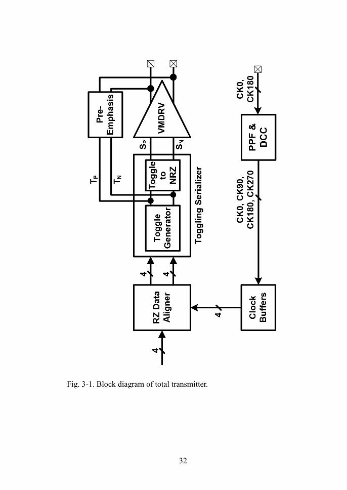
32
Fig. 3-1. Block diagram of total transmitter.

33
3.1. Quadrature Clock Generation
To avoid many challenges associated with global multiple phase
clocking, input clock of our transmitter is differential. Then four phase
clocks which are needed in parallel data align block are generated from
two stage passive PPF [8] and phases are controlled by DCC as shown
in Fig. 3-2. Quadrature phase of PPF are distorted due to passive
component characteristics that are frequency dependent. DCC followed
by PPF compensates phase distortion with delay control for following
buffers. Fig. 3-3 shows simulation results of phase distortion of PPF as
operation frequency and phase compensation range of DCC. Phase delay
of quadrature clock varies from 125ps to 145ps as the operation
frequency changes from 1GHz to 2GHz and the phase delay range from
DCC is about 53ps which can cover the phase delay variation of PPF.

34
CLKP
CLKN
CK0CK90
CK180CK270
Polyphase Filter
CK0
CK180
CK90
CK270CK0
CK180CK90
CK270CK0
CK180
ToData Aligner
Duty Cycle Corrector
Fig. 3-2. PPF and DCC for quadrature clock generation.
Fig. 3-3. Simulation results of phase distortion of PPF as operation
frequency and phase compensation range of DCC.

35
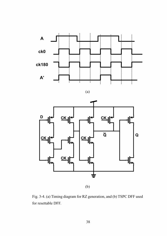
3.2. Resettable DFF and Toggle to NRZ
For proper extraction of data transition information, parallel input
data need data format conversion to RZ format. This operation can easily
be acquired with resettable DFFs which are used to align parallel data
for serialization. When each four parallel input data are aligned
according to each quadrature clock in each DFF, 180 degree shifted clock
of each phase also is delivered as reset signal. For example, input data A
is aligned with 0 degree clock, ck0, and reset to the ‘zero’ with 180
degree clock, ck180, then converted to RZ format data A′ as shown in
Fig. 3-4 (a). TSPC DFF is used for low power implementation as shown
in Fig. 3-4 (b). We use PMOS adopted to the �̅� signal for reset
operation. This approach can allow us to use the clock for reset signal
without using 180 degree shifted clock because the use of PMOS has an
inverting effect. Using PMOS reset, we can eliminate fan-out mismatch
of quadrature clock and phase offset problem between sampling clock
and reset clock.
The toggle signal can be generated with simple SR-Latch operation
and, as the generated signal from SR-Latch is the final serialized output,
high speed operation of SR-Latch is needed for clear serialized output
data generation. However, the relationship between serialized output

36
data and toggle signal needs SR-Latch with NOR gate as mentioned
before. As he NOR gate have three stack structure and employs two of
three stacks PMOS, the operation speed of SR-Latch with NOR gate is
slower than that of SR-Latch with NAND gate. For operation speed
enhance, we change the SR-Latch structure as shown in Fig. 3-5 (b). In
our push-pull structure SR-Latch alleviate three problems in
conventional SR-Latch structure with NOR gate. First, stack number. In
conventional structure, voltage headroom problem for high-speed
operation as three stacked need more VDS. Second, the use of PMOS.
The conventional structure employs two-stacked PMOS which have
slower majority carriers. Moreover, two PMOS are used for input
transistors that causes more operation speed degradation. Third, the duty
cycle. Output latch stage have unbalanced structure due to the third-
stacked PMOS transistors result in the distorted duty cycle. In our push-
pull structure, third-stacked PMOS are eliminated and input transistors
are replaced NMOS with cross input receiving. When the TP is high,
upper side NMOS of output signal S pushes the current generating high-
state output. When the TN is high, lower side NMOS of output signal S
pull the current generating low-state output. When both of two toggle
signals are low, input transistors are off and output signal is maintain
before state with latch operation. As the final latch stage have a balanced

37
structure due to the elimination of third stacked PMOS transistors. Fig.
3-6 shows the simulation eye diagrams of conventional and our push-
pull SR-Latch operation with 8 Gb/s. For simulation, both type of SR-
Latches are sized same to consume same power and same output
capacitor is loaded. With conventional structure, output eye diagram
shows ISI resulted from the low operation speed and distorted crossing
point and duty cycle. However, we can see that the improved output eye
diagram with our structure in the aspect of ISI and duty cycle from 17.5%
to 42.5%.
38
A
ck0
ck180
A'
(a)
D
CK
CK
CK
CK
CK
(b)
Fig. 3-4. (a) Timing diagram for RZ generation, and (b) TSPC DFF used
for resettable DFF.

39
TP
TP
TN
TN
SP SN
(a)
TP
TN
TN
TP
SP SN
(b)
Fig. 3-5. (a) NOR gate based SR-Latch, and (b) push-pull SR-Latch.

40
(a)
(b)
Fig. 3-6. Simulation results of (a) conventional SR-Latch, and (b) push-
pull SR-Latch.

41
3.3. Voltage-Mode Output Driver with Pre-Emphasis
Output driver generally realized with current-mode or voltage-mode.
Current-mode output driver (CMLDRV) is easy to set output impedance
for impedance matching but consumes more power than voltage-mode
output driver (VMDRV). In contrast, voltage-mode output driver
consumes four time less power than current-mode output driver with
differential operation but need complex circuits for output impedance
matching. The complexity gets worse with pre-emphasis. In CMLDRV,
the current summing is directly result in pre-emphasized output signal.
Just another branch which shares output resistor of main driver is needed
maintaining output impedance. However, in VMDRV, pre-emphasis
operation needs voltage summing which is more complex and difficult.
Various circuit techniques have been proposed for pre-emphasis such as
hybrid current-mode [9], resistive divider [10], channel-shunting [11],
and impedance modulation [12]. In these, pre-emphasis tap coefficients
are controlled with output stage segmentation [10]-[12], which needs
additional serializer or complex high-speed pre-drivers and,
consequently, increases power consumption.
In our transmitter, VMDRV is used for low power consumption. Fig.
3-7 shows VMDRV and basic operation. When serializer output SP is

42
high and SN is low, output driver current IDRV flows like Fig. 3-7 (b)
making high state of TXP and low state of TXN. When serializer output
SN is high and SP is low, output driver current IDRV flows like Fig. 3-7 (c)
making high state of TXN and low state of TXP. In addition, same
structure of VMDRV is used simply for current boosting 2-tap pre-
emphasis [12] with toggle signals. Fig. 3-8 shows schematics of
VMDRV with pre-emphasis. Pre-emphasized output signals, TXP and
TXN, are generated with serialized output data, SP and SN, and toggle
signals, TP and TN. As mentioned before, serialized output data are
emphasized according to the transition information in toggle signals in
output driver. The VMDRV output swing can be controlled with VDRV
which is set by regulator. VMDRV output impedance and pre-emphasis
boosting gain are controlled automatically with replica bias circuits.
Fig. 3-9 shows regulator and replica circuit for impedance matching.
The virtual supply voltage VDRV is set equal to the REF_VDRV by
regulator and output swing level is controlled equal to the 1/2VDRV by
output driver replica circuit ranging from 100 to 300 mVppd. The output
impedance is controlled by replica bias circuit which use resistive
voltage division. With 2Z0 load impedance, voltage level of node P and
node N are set to 3/4VDRV and 1/4VDRV, respectively, by negative
feedback. Then, upper side and lower side output impedance are

43
determined by Z0 automatically by resistive voltage division with proper
voltage of VZP and VZN. All the size of transistors in replica circuit are
16 times smaller than those in main output driver for power saving in
replica circuit.
Fig. 3-10 shows regulator and replica circuit for pre-emphasis and
boosting gain control. Pre-emphasis boosting gain is set by controlling
the boosting current IEQ in replica circuit. Boosting current, IEQ, for
wanted pre-emphasis boosting gain is
GEQ(dB) = 20 log (1 +𝐼𝐸𝑄𝑅𝑇𝑋
2𝑉𝐷𝑅𝑉). (3-1)
Because TXP and TXN are pre-emphasized with current boosting
rather than de-emphasis, the output signals maintain the DC voltage level
even with different equalization gain. The pre-emphasis boosting current
for target equalization gain is set by external control voltages
EQ_CONTP and EQ_CONTN with pre-emphasis current controller, and
bias voltages VEQP and VEQN are fed into pre-emphasis. By using
toggle signal from the serializer and achieving current boosting with the
impedance control, there is no additional or complex pre-driver stage for
pre-emphasis. All the transistors in the pre-emphasis current controller
are also 16 times smaller than those in pre-emphasis for power saving.

44
Z0
Z0
2Z0
TXP
TXN
SP
SN
VZN
VZP
VDRV
(a)
Z0
Z0
2Z0
TXP
TXN
SP
SN
VZN
VZP
VDRV
IDRV
IDRV
IDRV
IDRV
(b)

45
Z0
Z0
2Z0
TXP
TXN
SP
SN
VZN
VZP
VDRV
IDRV
IDRV
IDRV
IDRV
(c)
Fig. 3-7. Schematic of VMDRV (a), VMDRV operation with high SP
and low SN state, and VMDRV operation with high SN and low SP state.

46
TX
P
TX
N
SP
TP
TN
VZ
N
VZ
P
VE
QN
VE
QP
VD
RV
VE
Q
SN
SP
TP
TN
TX
P
TX
NTP
TN
SN
Fig. 3-8. Schematic of VMDRV with pre-emphasis.

47
VM
DR
V
Re
pli
ca D
RV
VD
D_D
RV
VD
D
VD
RV
RE
F_V
DR
V
16
Z0
16
Z0
32
Z0
VD
D
VD
RV
3/4
VD
RV
1/4
VD
RV
VZ
N
VZ
P
P N
Fig. 3-9. Regulator and replica circuit for impedance matching.

48
Pre
-Em
ph
as
is
Rep
lic
a P
re-E
mp
.
VD
D_E
QV
DD
VE
Q
RE
F_V
EQ
VE
Q
VE
Q
VD
D
VD
D
VE
QN
VE
QP
EQ
_C
ON
TP
EQ
_C
ON
TN
48
Z0
48
Z0
I EQ
I EQ
Fig. 3-10. Regulator and replica circuit for pre-emphasis and boosting
gain control.

49
3.4. Power Consumption Comparison
Using data transition information, much of powers in clock buffers,
pulse generators and complex pre-drivers can be saved. For power
comparison between conventional transmitter and our transmitter, we
designed another conventional 4:1 transmitter. The overall block
diagrams of the circuits used for comparison are shown in Fig. 3-11. Both
transmitters receive external differential clocks and generate quadrature
clocks with polyphaser filter and duty cycle corrector. 4:1 serializer and
pulse generator in the conventional transmitter are composed of CMOS
logic gates having the same fan-out strength of 2 for fair comparison. Fig.
3-12, Table 3-1, Fig. 3-13, and Table 3-2 shows the detail blocks used
for power consumption analysis of the conventional transmitter, power
consumption analysis of conventional transmitter, detail blocks used for
power consumption analysis of our transmitter, and power consumption
analysis of our transmitter, respectively, using dynamic power
consumption with
𝑃𝑑𝑦𝑛𝑎𝑚𝑖𝑐 =1
2(𝐶 𝑉2𝛼 𝑓 𝑁), (3-2)
where C is load capacitance, V is supply voltage, α is transition density,
f is operation frequency, and N is number of blocks. In conventional
transmitter, additional serializer for per-emphasis consumes as same

50
power as main serializer and clock buffers and pulse generator consumes
much power of 62.5 %. In our transmitter, power consumption ratio is
somewhat different to the conventional transmitter. First, RZ data aligner
has double transition density than conventional data aligner. Second, the
2NAND in toggling serializer half transition density than that of
conventional serializer because the transition information in parallel
input data are split into two toggle signals, positive toggle signal and
negative toggle signal. Finally, clock buffers for RZ data aligner have
more load capacitance because of the reset PMOS in the resettable DFF.
From the power analysis, we can see that our transmitter consumes less
power as 62.5% than conventional transmitter.
Fig. 3-14 shows the simulated power consumption of conventional
and our transmitter at 8 Gb/s in 65nm CMOS technology. Because our
transmitter does not need any pulse generator, nor any extra serializer
needed for pre-emphasis, and the power consumption can be reduced as
analyzed before. The simulation result shows 25% reduction of power
consumption for our transmitter.
In conventional serializer, final serializing is performed with clock
signals which finally align data to the clean clock. However, in toggling
serializer, serializing is performed not with clock signals but with data
transition information without timing information in clock, causing jitter
51
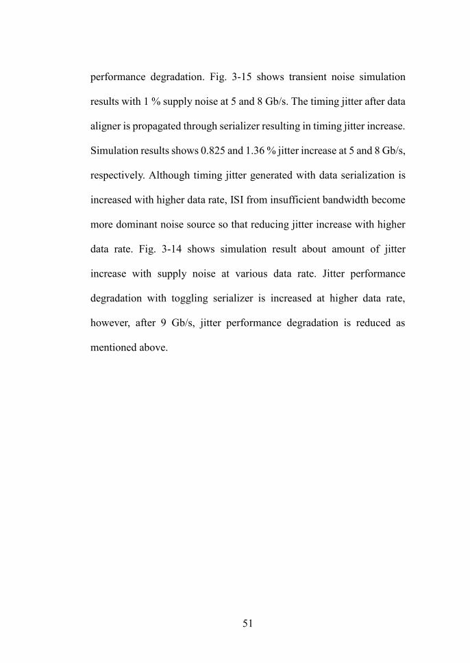
performance degradation. Fig. 3-15 shows transient noise simulation
results with 1 % supply noise at 5 and 8 Gb/s. The timing jitter after data
aligner is propagated through serializer resulting in timing jitter increase.
Simulation results shows 0.825 and 1.36 % jitter increase at 5 and 8 Gb/s,
respectively. Although timing jitter generated with data serialization is
increased with higher data rate, ISI from insufficient bandwidth become
more dominant noise source so that reducing jitter increase with higher
data rate. Fig. 3-14 shows simulation result about amount of jitter
increase with supply noise at various data rate. Jitter performance
degradation with toggling serializer is increased at higher data rate,
however, after 9 Gb/s, jitter performance degradation is reduced as
mentioned above.

52
(a)
(b)
Fig. 3-11. Block diagram for power comparison simulation: (a)
conventional transmitter, (b) transmitter with toggling serializer.

53
DP
DN
Data Aligner
Serializer
4
4
4
CK0 & CK90
& CK180 & CK270
Pulse Gen.
Serializer
for Pre-Emp.
4
4
4
4
4
DFF
DFF
DFF
DFF
Clock
Buffers
4
Clock
Buffers
Fig. 3-12. Detail block diagram of conventional transmitter used for
power consumption analysis.

54
TABLE 3-1
DYNAMIC POWER CONSUMPTION ANALYSIS
OF CONVENTIONAL TRANSMITTER
Normalized
Parameters Power
Ratio C α f N
Data Align 2 1 1 8 16
Serializer
2NAND 1 1 1 8
16
4NAND 1 1 4 2
Add.
Serializer
2NAND 1 1 1 8
16
4NAND 1 1 4 2
Pulse Gen. 4 2 1 4 32
Clock
Buffers
Data Align 2 2 1 4
48
Pulse Gen. 4 2 1 4
Total 128

55
DP
DN
CK0 & CK90
& CK180 & CK270
RZ Data Aligner
Toggling Serializer
TP
TN
DFF
DFF
DFF
DFF
4
4
4
4
Toggle
To
NRZ
4
Clock
Buffers
Fig. 3-13. Detail block diagram of our transmitter with toggling
serializer used for power consumption analysis.

56
TABLE 3-2
DYNAMIC POWER CONSUMPTION ANALYSIS
OF OUR TRANSMITTER WITH TOGGLING SERIALIZER
Normalized
Parameters Power
Ratio C α f N
RZ Data Align 2 2 1 8 32
Toggling
Serializer
2NAND 1 0.5 1 8 4
4NAND 2 1 4 2 16
Toggle to NRZ 1 1 4 2 8
Clock
Buffers Data Align 2.5 2 1 4 20
Total 80

57
3.0
2
2.2
6
Fig. 3-14. Simulated power consumption of conventional and our
proposed transmitter at 8 Gb/s in 65nm CMOS, respectively.

58
Co
nven
tio
nal
Seri
ali
zer
To
gg
lin
g
Seri
ali
zer
5G
b/s
8G
b/s
4.8
8%
Jit
ter
6.1
ps
6.2
4%
Jit
ter
7.8
ps
1.9
75%
Jit
ter
3.9
5p
s
2.8
% J
itte
r
5.6
ps
0.8
25
% J
itte
r In
cre
ase
1.3
6%
Jit
ter
Incre
ase
Fig. 3-15. Transient noise simulation with 1 % supply noise at 5 and 8
Gb/s.
59
4 5 6 7 8 9 10 110.0
0.5
1.0
1.5
2.0
2.5
3.0
Incre
ased
Jit
ter
(UI)
Data Rate (Gb/s)
Fig. 3-16. Simulated jitter increase with supply noise at various data
rate.
60
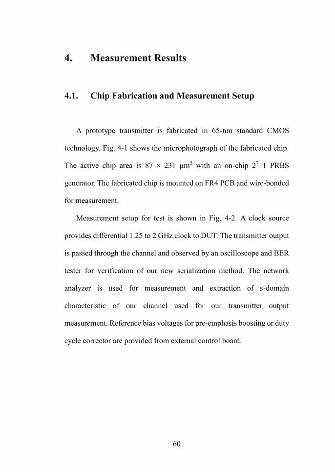
4. Measurement Results
4.1. Chip Fabrication and Measurement Setup
A prototype transmitter is fabricated in 65-nm standard CMOS
technology. Fig. 4-1 shows the microphotograph of the fabricated chip.
The active chip area is 87 × 231 μm2 with an on-chip 27–1 PRBS
generator. The fabricated chip is mounted on FR4 PCB and wire-bonded
for measurement.
Measurement setup for test is shown in Fig. 4-2. A clock source
provides differential 1.25 to 2 GHz clock to DUT. The transmitter output
is passed through the channel and observed by an oscilloscope and BER
tester for verification of our new serialization method. The network
analyzer is used for measurement and extraction of s-domain
characteristic of our channel used for our transmitter output
measurement. Reference bias voltages for pre-emphasis boosting or duty
cycle corrector are provided from external control board.

61
AVMDRV &
Pre-emphasis
B
RZ Data Aligner &
Toggling Serializer &
Buffers & Pre-driver
C 27-1 PRBS Generator
D PPF & DCC
Fig. 4-1. Chip microphotograph of our transmitter.

62
Ch
an
ne
l
(40
cm
PC
B t
race
+ 5
0cm
SM
A c
ab
le) [E
ye
dia
gra
m m
on
ito
rin
g
aft
er
the
ch
an
nel]
[Eye
dia
gra
m m
on
ito
rin
g
be
fore
th
e c
han
ne
l]
[Ch
an
ne
l
ch
ara
cte
risti
c]
Pre
-em
ph
asiz
ed
da
ta
(5 –
8 G
b/s
)
Su
pp
ly v
olt
ag
e
(0.8
- 1
V)
Clo
ck
So
urc
e
Bia
s R
efe
ren
ces
Bo
os
tin
g G
ain
Du
ty C
ycle
Oscil
los
co
pe
Ne
two
rk
An
aly
ze
r
Oscil
los
co
pe
Po
we
r
Su
pp
ly
Tra
ns
mit
ter
DU
T
Dif
fere
nti
al C
lock
(1.2
5 –
2 G
Hz)
Fig. 4-2. Measurement setup.
63
4.2. Eye Diagram and Energy Efficiency
The transmitter is tested with 27–1 PRBS data from the on-chip
generator. The output of transmitter is measured directly without channel
for operation verification. Fig. 4-3 shows the transmitter output eye
diagram with various swing level at 8 Gb/s. By setting the reference
voltage of regulator for virtual supply for output driver, the output swing
is changed from 100 to 300 mVppd. The transmitter is tested with 5 to 8
Gb/s under various supply voltage from 0.8 to 1 V for low power
operation. Supply voltages are scaled down at each data rate to have
minimum 100 mVppd eye height and 0.6 UI eye width except for
VMDRV and pre-emphasis which are fixed at 0.5 V. The transmitter
output is pre-emphasized with toggle signals with boosting gain by 6 dB.
Fig. 4-4 shows the transmitter output eye diagrams which have 150
mVppd fixed DC swing level, without and with pre-emphasis of 6-dB
boosting gain at 5 and 8 Gb/s.
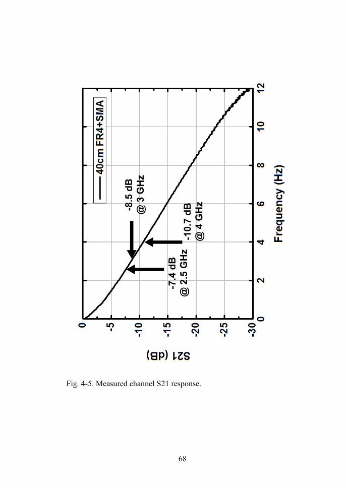
Pre-emphasized output of transmitter is passed through the 40 cm
FR4 trace and 50 cm SMA cable as the channel, which have measured
loss of 7.4 and 10.7 dB at 2.5 and 4 GHz, respectively, for pre-emphasis
effect verification. Fig. 4-5 shows the measured channel S21 response.
Without pre-emphasis, output eye diagram is distorted showing small

64
eye opening at 5 Gb/s and almost closed eye diagram at 8 Gb/s. With 6-
dB pre-emphasis, however, the output eye diagram is more opened with
115 mVppd eye height and 140 ps eye width and 60 mVppd eye height and
63 ps eye width at 5 Gb/s and 8 Gb/s, respectively. The measured eye
diagrams of channel output are shown in Fig. 4-6.
Fig. 4-7 shows measured energy efficiency of our transmitter at
different data rates and comparison with previously reported low-power
transmitters in 65nm CMOS. Our transmitter achieves energy efficiency
of 0.202 to 0.303 pJ/bit for 5 to 8 Gb/s without pre-emphasis and 0.252
to 0.333 pJ/bit for 5 to 8 Gb/s with pre-emphasis, respectively. Without
pre-emphasis, our transmitter can achieves lower power consumption
than that of other transmitters with toggle signal which can eliminate
pulse generator and many clock buffers for serialization. With pre-
emphasis, our transmitter shows much improved energy efficiency with
the use of data transition information for pre-emphasis eliminating the
use of full-rate speed clock or additional serializer for 1-bit delayed data
generation. The power consumption of [5] shows worse energy
efficiency than our and other transmitter, even though the power
consumption of [6] is measured without 0-dB boosting. This indicates
that the effect of using data transition information is more effective with
pre-emphasis.

65
Table 4-1 gives more detailed performance comparison for various
transmitters realized in 65nm CMOS. Our transmitter shows better
energy efficiency than [5] and [6] at 6 Gb/s and [7] at 8 Gb/s by the factor
of 1.36 and 2.16, respectively. For direct comparison with swing
variation, the power consumption of total transmitter is divided by the
output swing voltage. Though direct division of total power consumption
by output swing has some disadvantage for our transmitter, our
transmitter still shows better normalized energy efficiency. When the
power consumption for equalization is considered, the energy efficiency
of our transmitter at 8 Gb/s is better than that of [7] at 12 Gb/s by the
factor of 2.4 under almost same channel loss. Such comparison confirms
that our proposed transmitter with data transition information efficiently
reduces power consumption and the energy efficiency can be further
enhanced with pre-emphasis.
66
50mV 20ps
300mVppd
50mV 20ps
100mVppd
50mV 20ps
200mVppd
Fig. 4-3. Measured transmitter output eye diagram with various swing
level.

67
w/o
Equ
aliz
ation
6dB
Eq
ua
lizatio
n
Tra
nsm
itte
r O
utp
ut
5 Gb/s 8 Gb/s
50mV 20ps50mV 50ps
Width : 145ps
Height : 118mVppd
Width : 77ps
Height : 110mVppd
Fig. 4-4. Measured transmitter output eye diagram with and without pre-
emphasis at 5 and 8 Gb/s having 150mVppd output DC swing.
68
-7.4
dB
@ 2
.5 G
Hz
-10.7
dB
@ 4
GH
z-8.5
dB
@ 3
GH
z
Fig. 4-5. Measured channel S21 response.

69
w/o
Equa
lization
6dB
Equa
lization
Ch
ann
el O
utp
ut
5 Gb/s 8 Gb/s
Width : 140ps
Height : 115mVppd
Width : 63ps
Height : 60mVppd
50mV 20ps50mV 50ps
Fig. 4-6. Measured channel output eye diagram with and without pre-
emphasis at 5 and 8 Gb/s.

70
Fig. 4-7. Measured energy efficiency and comparison.

71
TABLE 4-1
DETAILED PERFORMANCE SUMMARY AND COMPARISON
[5]
[6]
[7]
This
work
Technolo
gy
65 n
m65 n
m65 n
m65 n
m
Supply
Voltage (
V)
0.6
-0.8
0.4
5-0
.70.7
5-1
0.8
[5G
b/s
], 0
.85 [6G
b/s
], 1
[8G
b/s
]
Data
Rate
(G
b/s
)4.8
-81-6
8-1
65-8
Outp
ut S
win
g (
mV
pp,d)
100-2
00
200
100-3
00
10
0-3
00
Energ
y E
ffic
iency w
/o
PE
(pJ/b
it)
[Data
rate
, S
win
g
Voltage]
0.3
[6.4
Gb/s
,
150m
Vpp,d]
0.3
1
[6G
b/s
,
200m
Vpp,d]
0.6
5
[8G
b/s
,
300m
Vpp,d]
0.2
02
[5G
b/s
,
150m
Vpp,d]
0.2
2
[6G
b/s
,
150m
Vpp,d]
0.3
[8G
b/s
,
150m
Vpp,d]
Energ
y E
ffic
iency w
/o
PE
per
Outp
ut V
oltage
Sw
ing (p
J/b
it/V
)
21.5
52.1
71.3
51.4
72
Energ
y E
ffic
iency w
/
PE
(pJ/b
it)
[Data
rate
, S
win
g
Voltage]
N/A
N/A
0.8
1
[12G
b/s
,
300m
Vpp,d]
0.2
52
[5G
b/s
,
300m
Vpp,d]
0.2
69
[6G
b/s
,
300m
Vpp,d]
0.3
33
[8G
b/s
,
300m
Vpp,d]
Channel Loss
N/A
N/A
-12dB
@
6G
Hz
-7.4
dB
@
2.5
GH
z
-8.5
dB
@
3G
Hz
-10.7
dB
@
4G
Hz

72
4.3. Summary
We proposed a low-power wireline transmitter with a novel serializer
based on data transition information. For low power consumption,
parallel data are serialized with toggle signals which are extracted from
adjacent parallel data, rather than with short pulse-clock signals. For
NRZ signal generation from toggle signals, a novel push-pull based SR-
Latch is used which improves not only the operation speed but also duty
cycle. In pre-emphasis, the direct use of toggle signals from serializer
and current boosting equalization with impedance control effectively
reduces circuit complexity and saves power. With these, our transmitter
achieves the lowest energy efficiency among wireline transmitters
realized in 65nm CMOS technology.

73
5. Application Extension
Having been used in optical communications and recently moving
into electrical systems [13]–[17], duobinary modulation can achieve a
data rate theoretically twice as much as the channel bandwidth. Inter-
symbol interference (ISI) is introduced in a controlled manner such that
it can be cancelled out to recover the original signal. Unlike PAM4 and
NRZ signals, duobinary signals incorporate the channel loss as part of
the overall response [14], substantially reducing the required boost and
relaxing the equalizer design. A duobinary signal is originally defined as
the sum of the present bit and the previous one of a binary sequence [18]:
𝑤[𝑛] = 𝑥[𝑛] + 𝑥[𝑛 − 1]. (5-1)
It correlates two adjacent bits to introduce the desired ISI. Considering
the equivalent linear model as shown in Fig. 5-1, we have the transfer
function H(f) as
𝐻(𝑓) =𝑊(𝑓)
𝑋(𝑓)=
1
2[1 + exp (−𝑗2𝜋𝑓𝑇𝑏)]. (5-2)
where Tb denotes the bit period, and the attenuating factor 1/2 is used to
equalize the total power of x(t) and w(t). It can be also shown that the
duobinary spectrum SW(f) is given by
𝑆𝑊(𝑓) = 𝑐𝑜𝑠2(π𝑓𝑇𝑏) ∙ 𝑇𝑏 [sin(π𝑓𝑇𝑏)
π𝑓𝑇𝑏]
2
. (5-3)
= 𝑇𝑏 [sin(2π𝑓𝑇𝑏)
2π𝑓𝑇𝑏]
2
. (5-4)

74
As shown in Fig. 5-1(b), SW(f)is still a sinc function but with only
half the bandwidth as compared with SX(f). In other words, the duobinary
coding “squeezes” the spectrum toward the dc line, and reduces the
required channel bandwidth by 50%. Note that almost 90% of the signal
power stays in the main lobe of a sinc function. To further clarify the
analysis, we apply the NRZ and duobinary data through a brickwall filter
cutting off at half data rate 1/(2Tb). As can be shown in Fig. 5-2, the
received NRZ data suffers from 81.8% ISI and 0.8-UI jitter, whereas the
duobinary is almost unaffected. It is because the former loses 51.4% of
the power but the latter loses only 10% [19]-[20].

75
(a)
(b)
Fig. 5-1. (a) Linear model of duobinary signaling. (b) Composition of
duobinary spectrum.

76
(a)
(b)
Fig. 5-2. Output spectra and waveforms for different data formats
passing through an ideal filter. (a) NRZ. (b) Duobinary.

77
5.1. Duobinary with Toggle Signals
5.1.1. Relationship between Duobinary and Toggle
Signals
Data transition information extracted from toggling serializer can
directly be used to generate duobinary signal. We can find out the
relationship among serialized signal, toggle signals, and duobinary
signal by looking over the timing diagram as shown in Fig. 5-3. Some
kinds of cases are repeated in the timing diagram. First, when serialized
signal and toggle signals are all ‘zero’, then duobinary signal has ‘zero’
level. Second, when serialized signal is ‘zero’ and positive toggle signal,
TP, is ‘zero’ and negative toggle signal, TN, is ‘one’, then duobinary
signal has ‘one’ level. Third, when serialized signal is ‘one’ and positive
toggle signal, TP, is ‘one’ and negative toggle signal, TN, is ‘zero’, then
duobinary signal has also ‘one’ level. Finally, when serialized signal is
‘one’ and toggle signals are all ‘zero’, then duobinary signal has ‘two’
level. All states are summarized in Table 5-1. This relationship can be
occur because the duobinary signal modulation uses the data transition
information between adjacent data, and toggle signals also have that
information.
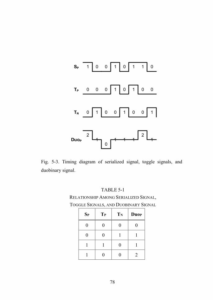
78
SP
TP
TN
DuoP
1 0 0 1 0 1 1 0
0 0 0 1 0 1 0 0
0 1 0 0 1 0 0 1
21
01 1 1
21
Fig. 5-3. Timing diagram of serialized signal, toggle signals, and
duobinary signal.
TABLE 5-1
RELATIONSHIP AMONG SERIALIZED SIGNAL,
TOGGLE SIGNALS, AND DUOBINARY SIGNAL
SP TP TN DuoP
0 0 0 0
0 0 1 1
1 1 0 1
1 0 0 2

79
5.1.2. Voltage-Mode Duobinary Output Driver with
Toggle Signals
To use the relationship examined above to the voltage-mode output
driver, it is necessary to look at the impedance matching of voltage mode
output driver with duobinary signaling. Fig. 5-4 shows two cases of the
impedance matching. When the duobinary signal has ‘one’ level,
equivalent resistance model of voltage-mode output driver and load
resistance is shown in Fig. 5-4 (a). In that case, output impedance at DuoP
and DuoN nodes are Z0 (2Z0//2Z0) and voltage level of DuoP and DuoN
are 1/2VDRV which indicates ‘one’ level in duobinary signaling. When
the duobinary signal has ‘zero’ or ‘two’ level, equivalent resistance
model of voltage-mode output driver and load resistance is shown in Fig.
5-4 (b). In that case, output impedance at DuoP and DuoN nodes also Z0
and voltage level of DuoP and DuoN are 3/4VDRV or 1/4VDRV which
indicate ‘two’ or ‘zero’ level in duobinary signaling.
For implementation, we use impedance modulation method to the
voltage-mode duobinary output driver. Fig. 5-5 shows our voltage-mode
duobinary output driver and output states with serialized output signals
and toggle signals are given in Table 5-2. For impedance modulation,
transition toggle signal, TT, is added which is generated from positive

80
and negative toggle signals with XNOR operation. For delay matching,
the structure of XNOR gate which is used for TT signal generation, is
CMOS inverter based structure as shown in Fig. 5-6 (a). When toggle
signals have transition, TT has ‘zero’ and when the toggle signals have
non-transition, TT has ‘one’. This XNOR gate can be used for inverter
buffer in pre-driver stage with turn on state of upper and lower transistors
as shown in Fig. 5-6 (b).
Fig. 5-7 shows voltage-mode duobinary output driver with replica
bias circuit having ‘one’ state. For example, when the SP, SN, TP, TN, and
TT have ‘one’, ‘zero’, ‘one’, ‘zero’, and ‘zero’, respectively, as shown in
Fig. 5-7, the output state of DuoP and DuoN have ‘one’ level. The replica
bias circuits generate bias voltage of H_B and L_B nodes for impedance
matching with duobinary ‘one’ level. Fig 5-6 shows voltage-mode
duobinary output driver with replica bias circuit having ‘two’ or ‘zero’
states. For example, when the SP, SN, TP, TN, and TT have ‘one’, ‘zero’,
‘zero’, ‘zero’, and ‘one’, respectively, as shown in Fig. 5-8, the output
state of DuoP and DuoN have ‘two’ and ‘zero’ level, respectively. The
replica bias circuit generates bias voltage of TH_B and TL_B nodes for
impedance matching with duobinary ‘two’ and ‘zero’ level.

81
VDRV
DuoP
DuoN
2Z0
Z0
Z0
VDRV
3/4VDRV
1/4VDRV
GND
(a)
VDRV
DuoP DuoN
2Z0
2Z0
2Z0
VDRV
1/2VDRV
GND
VDRV
2Z0
2Z0
(b)
Fig. 5-4. Equivalent resistance model of duobinary voltage mode output
driver and voltage level of ‘two’ and ‘zero’ level case (a), and ‘one’ level
case (b).

82
TN SP
TP SN
TPSN
TNSP
H_B
L_B
TH_B
TL_B
TT
TT
VDRV
DuoP
DuoN
2Z0
Fig. 5-5. Voltage-mode duobinary output driver with toggle signal.
TABLE 5-2
TRUTH TABLE FOR DUOBINARY DRIVER
SP SN TP TN TT DuoP DuoN
0 1 0 0 1 0 2
0 1 0 1 0 1 1
1 0 1 0 0 1 1
1 0 0 0 1 2 0

83
BB B
A
B
A
AB
BB
AB
(a)
GND GND
A
A
VDD
B
B
VDD
(b)
Fig. 5-6. Inverter based XNOR gate (a), and use of XNOR gate as
inverter buffer (b).
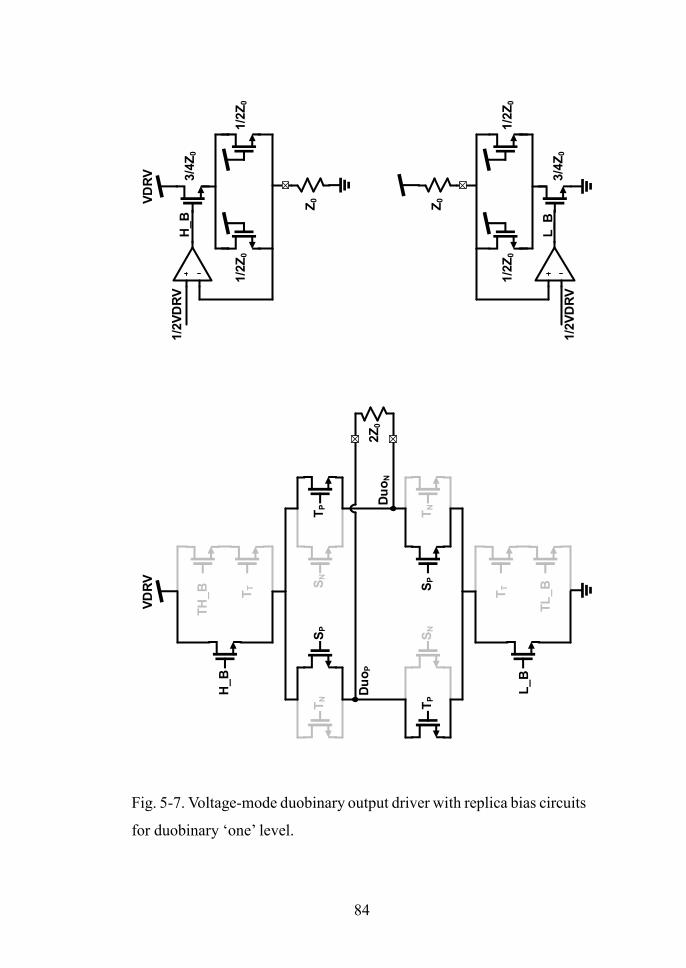
84
TN
SN
SN
TN
TH
_B
TL
_B
TT
TT
SP
TP
TP
SP
H_B
L_B
VD
RV
Du
oP
Du
oN
2Z
0
H_B
L_B
VD
RV
Z0
Z0
1/2
VD
RV
1/2
VD
RV
1/2
Z0
1/2
Z0
3/4
Z0
1/2
Z0
1/2
Z0
3/4
Z0
Fig. 5-7. Voltage-mode duobinary output driver with replica bias circuits
for duobinary ‘one’ level.

85
TP
SN
TP
SN
TN
TN
SP
SP
H_B
L_B
TH
_B
TL
_B
TT
TT
VD
RV
Du
oP
Du
oN
2Z
0
H_B
L_B
TH
_B
TL
_B
VD
RV
2Z
0
1/2
Z0
1/2
Z0
3/4
Z0
3/4
Z0
3/2
Z0
3/2
Z0
3/4
VD
RV
1/4
VD
RV
Fig. 5-8. Voltage-mode duobinary output driver with replica bias circuit
for duobinary ‘two’ and ‘zero’ level.

86
5.1.3. Duobinary Receiver with 1-Tap DFE
The transmitted duobinary data value takes one of three levels (two,
one, zero) depending on the present and previous values of serialized
data. The receiver should converts the incoming duobinary data into a
NRZ data by performing the (1 (1 + 𝑍−1)⁄ ) operation. Because the
signaling has three levels, two reference voltage values, VH and VL, are
needed for conversion. VH is the mid-point voltage of the highest ‘two’
level and the middle ‘one’ level; VL is the mid-point voltage of the
middle ‘one’ level and the lowest ‘zero’ level. The duobinary signaling
consists of relation between previous data and present data, the present
reference voltage needs to be changed to VH of VL according to the
previous decision data in the receiver. If the previous decision data is
binary ‘one’ or ‘zero’, the reference voltage is set to VH (‘one-point-five’)
or VL (‘zero-point-five’), respectively. This operation for changing the
reference voltage depending on the previous decision data corresponds
to the subtraction of the previous decision data from the present input
data. Although this process is identical to the 1-tap DFE operation with
the tap-coefficient of 1, it performs the duobinary-to-NRZ conversion
and does not compensate for ISI generated by a lossy transmission
channel [21]-[23].

87
The duobinary-to-NRZ converter circuit consists of even and odd
flip-flops driven by two half-rate clock signals (CKE, CKO) as shown in
Fig. 5-9. Each flip-flop compares the incoming data to VREF. VREF is set
to either VH or VL depending on the previous decision data. The timing
diagram of duobinary-to-NRZ converter is shown in Fig. 5-10 [20]. This
architecture is similar to the direct feedback 1-tap DFE, but the
difference is that the tap-coefficient is fixed to 1.0.
The differential input, duobinary-to-NRZ converter consists of
duplicated differential strong-arm based comparator and SR-Latches as
shown in Fig. 5-11. The schematic of even side differential comparator
is also shown in Fig. 5-11.

88
Fig. 5-9. The concept of duobinary-to-NRZ converter.
SP
DIN
1 0 0 1 0 1 1 0
VH
VL
CKE
CKO
RDE
RDO
1 0 0 1
0 1 1 0
VH
VL
VL
VH
VL
VH
VH
Fig. 5-10. Timing diagram of duobinary-to-NRZ converter.

89
INP
INN
OU
TP
OU
TN
CK
E
DU
OP
DU
ON
RD
E,P
RD
E,P
VT
H,H
VT
H,L
10
RD
O,P
RD
O,N
VR
EF
INP
INN
OU
TP
OU
TN
CK
OR
DO
,P
RD
O,P
VT
H,H
VT
H,L
10
RD
E,P
RD
E,N
VR
EF
CK
EC
KE
CK
EC
KE
CK
E
INP
INN
OUTP
OUTN
RD
O,N
RD
O,P
RD
O,P
RD
O,N
VT
H,H
VT
H,L
VT
H,H
VT
H,L
Fig. 5-11. Differential duobinary-to-NRZ converter.

90
5.1.4. Implementation and Measurement Results
A prototype duobinary transmitter and receiver are fabricated in 65-
nm standard CMOS technology. Fig. 5-12 shows the microphotograph
of the fabricated chips. The active chip area of duobinary transmitter and
receiver are 87 × 242 μm2 with an on-chip 27–1 PRBS generator and 84
× 162 μm2, respectively. The fabricated chips are mounted on FR4 PCB
and wire-bonded for measurement.
Measurement setup for test is shown in Fig. 5-13. A pulse pattern
generator (PPG) provides differential 1.25 to 2 GHz clock or 27–1 PRBS
pattern synchronized clock to duobinary transmitter DUT for verification
of duobinary pattern generation. The transmitter output is observed by
an oscilloscope and passed to the receiver DUT. Receiver DUT is
provided 2 to 4 GHz half-rate clock from clock source. Reference bias
voltages for transmitter or reference voltage for decision level of receiver
are provided from external control board.
Fig. 5-14 shows the measured duobinary transmitter output eye
diagram at 5 Gb/s and 8 Gb/s. The differential peak-to-peak voltage is
150 mVppd and output eye diagram have minimum 162 ps width and 60
mVppd height opening and 75 ps width and 51 mVppd opening at 5 Gb/s
and 8 Gb/s, respectively.

91
Fig. 5-15 shows simulated eye pattern and measured eye pattern at 8
Gb/s. For measurement, 27–1 PRBS pattern synchronized clock is
provided from PPG equipment to the transmitter DUT. Measurement
result of transmitter pattern exactly matches to the simulated duobinary
pattern.
Fig. 5-16 shows measured 2 Gb/s receiver output eye diagram with
8 Gb/s duobinary transmitter output data. For measurement, half-rate
clock is provided from clock source to receiver DUT and NRZ converted
output data are de-muxed. Reference voltages of VH and VL are
externally controlled. To verify the duobinary-to-NRZ conversion of RX,
output data of RX are measured by BER tester. Fig. 5-17 shows the
measured Bathtub curve of receiver output and duobinary-to-NRZ
conversion is well performed.
Table 5-3 and Table 5-4 show the performance summary of
duobinary transmitter and receiver, respectively.
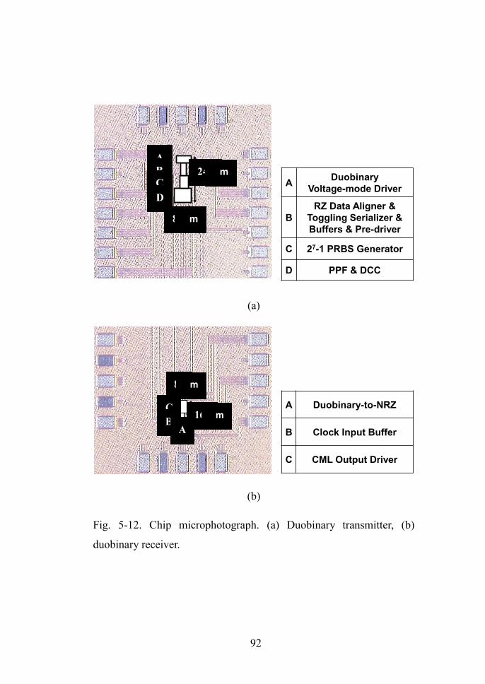
92
242μm
87μm
A
B
C
D
ADuobinary
Voltage-mode Driver
B
RZ Data Aligner &
Toggling Serializer &
Buffers & Pre-driver
C 27-1 PRBS Generator
D PPF & DCC
(a)
162μm
84μm
C
BA
A Duobinary-to-NRZ
B Clock Input Buffer
C CML Output Driver
(b)
Fig. 5-12. Chip microphotograph. (a) Duobinary transmitter, (b)
duobinary receiver.

93
[Eye
dia
gra
m o
f T
ran
sm
itte
r]
Oscil
los
co
pe
Tra
ns
mit
ter
DU
T
Dif
fere
nti
al C
lock
(1.2
5 –
2 G
Hz)
Re
ce
ive
r
DU
T
[Eye
dia
gra
m o
f R
ec
eiv
er]
Oscil
los
co
pe
[BE
R t
est
& B
ath
tub
]D
iffe
ren
tial C
lock
(2 –
4 G
Hz)
BE
RT
Sc
op
e
Duobinary Data
(5 – 8 Gb/s)
Qu
art
er-
rate
Rece
iver
Data
(2 G
b/s
)
PP
G
Clo
ck
So
urc
e
27–1 P
RB
S P
att
ern
Syn
ch
ron
ized
Clo
ck
Fig. 5-13. Measurement setup.

94
20mV 50ps
150mVppd 5 Gb/s
(a)
20mV 50ps
150mVppd 8 Gb/s
(b)
Fig. 5-14. Measured duobinary transmitter output eye diagram at 5 Gb/s
(a), and 8 Gb/s (b).

95
27–1 P
RB
S
Patt
ern
Sim
ula
ted
Du
ob
inary
Patt
ern
Mea
su
red
Du
ob
inary
Patt
ern
Fig. 5-15. Simulated PRBS pattern and duobinary pattern from 27–1
PRBS pattern and measured duobinary pattern.

96
Fig. 5-16. Measured duobinary receiver output eye diagram at 2 Gb/s.
Fig. 5-17. Measured Bathtub curve of duobinary receiver output at
2Gb/s.

97
TABLE 5-3
PERFORMANCE SUMMARY OF DUOBINARY TRANSMITTER
Technology 65 nm
Supply Voltage (V) 1
Data Rate (Gb/s) 5-8
Output Swing (mVpp,d) 100-200
Minimum Eye Opening (UI)
[Data Rate]
Width: 0.6
Height: 0.68
[8 Gb/s]
Power Consumption (mW)
[Data Rate, Swing Voltage]
2.8
[8 Gb/s, 150 mVpp,d]
Energy Efficiency (pJ/bit)
[Data Rate, Swing Voltage]
0.35
[8 Gb/s, 150 mVpp,d]
TABLE 5-4
PERFORMANCE SUMMARY OF DUOBINARY RECEIVER
Technology 65 nm
Supply Voltage (V) 1.2
Data Rate (Gb/s) 5-8
Clock Frequency (GHz) 2.5-5
Bit Error Rate
[PRBS Pattern]
<10-12
[27–1]
Power Consumption (mW)
[Data Rate]
2.56
[8 Gb/s]
Energy Efficiency (pJ/bit)
[Data Rate]
0.32
[8 Gb/s]

98
5.2. Duobinary with Consecutive Signals
5.2.1. Relationship Between Duobinary and Consecutive
Signals
Duobinary signal generation with data transition information using
toggle signal is effective but, voltage-mode duobinary output driver
needs so much input and bias control. Many stacked transistors make it
hard to match the output impedance to the channel impedance resulting
in large size of transistors and increasing power consumption. Instead of
using toggle signals with serialized signal for duobinary generation,
consecutive signals which also have data transition information can be
easily used for duobinary signal generation as shown in Fig. 5-18.
Consecutive signals, CH and CL, indicates that continuous high and
continuous low state in the serialized signal. We can find out the
relationship among serialized signal, consecutive signals, and duobinary
signal looking over the timing diagram in Fig. 5-18. Very simple patterns
are repeated in the timing diagram. First, when consecutive high signal
is ‘one’, then duobinary signal has ‘two’ level. Second, when consecutive
low signal is ‘one’, then duobinary signal has ‘zero’ level. Finally, all
consecutive signals are ‘zero’, then duobinary signal has ‘one’ level. All

99
states are summarized in Table 5-5.
SP
CH
CL
DuoP
1 0 0 1 0 1 1 0
1 0 0 0 0 0 1 0
0 0 1 0 0 0 0 0
21
01 1 1
21
Fig. 5-18. Timing diagram of serialized signal, consecutive signals, and
duobinary signal.
TABLE 5-5
RELATIONSHIP AMONG CONSECUTIVE SIGNAL,
AND DUOBINARY SIGNAL
CH CL DuoP
0 1 0
0 0 1
1 0 2

100
5.2.2. Consecutive Signal Generation
Consecutive signal can be extracted from input data comparing
adjacent two parallel data as shown in Fig. 5-19. Each four partial
consecutive high signal segments, CH,AB, CH,BC, CH,CD, CH,DA, are
combined by simple OR logic generating final consecutive high signal,
CH. Consecutive low signal, CL, is generated in the same way with
consecutive high signal. Only difference between consecutive signal
generation and toggle signal generation is parallel data connection to the
serializer.
Overall block diagram and timing diagram of consecutive serializer
is shown in Fig. 5-20. All the block of consecutive serializer are same
with toggling serializer except for the connection of parallel data to the
serializer and the absence of toggle to NRZ block. Logic operations for
consecutive high signal and consecutive low signal are given as
CH = (A′ ∙ B′) + (B′ ∙ C′) + (C′ ∙ D′) + (D′ ∙ A′)
= ((A′ ∙ B′)̅̅ ̅̅ ̅̅ ̅̅ ̅̅ ∙ (B′ ∙ C′)̅̅ ̅̅ ̅̅ ̅̅ ̅̅ ∙ (C′ ∙ D′)̅̅ ̅̅ ̅̅ ̅̅ ̅̅ ∙ (D′ ∙ A′)̅̅ ̅̅ ̅̅ ̅̅ ̅̅ )̅̅ ̅̅ ̅̅ ̅̅ ̅̅ ̅̅ ̅̅ ̅̅ ̅̅ ̅̅ ̅̅ ̅̅ ̅̅ ̅̅ ̅̅ ̅̅ ̅̅ ̅̅ ̅̅ ̅̅ ̅̅ ̅̅ ̅̅ ̅̅ (5-1)
CL = (A′̅ ∙ B′̅) + (B′̅ ∙ C′̅) + (C′̅ ∙ D′̅) + (D′̅ ∙ A′̅)
= ((A′̅ ∙ B′̅)̅̅ ̅̅ ̅̅ ̅̅ ̅̅ ∙ (B′̅ ∙ C′̅)̅̅ ̅̅ ̅̅ ̅̅ ̅̅ ∙ (C′̅ ∙ D′̅)̅̅ ̅̅ ̅̅ ̅̅ ̅̅ ∙ (D′̅ ∙ A′̅)̅̅ ̅̅ ̅̅ ̅̅ ̅̅ )̅̅ ̅̅ ̅̅ ̅̅ ̅̅ ̅̅ ̅̅ ̅̅ ̅̅ ̅̅ ̅̅ ̅̅ ̅̅ ̅̅ ̅̅ ̅̅ ̅̅ ̅̅ ̅̅ ̅̅ ̅̅ ̅̅ ̅̅ ̅̅ ̅
(5-2)
In (5-1) and (5-2), logic operations with AND gates and OR gates are
simply converted to NAND gates by Boolean algebra for easy

101
implementation. Logic operations produce consecutive high signal, CH,
indicating the serialized output should have continuous 1 and,
consecutive low signal, CL, indicating continuous 0. Consecutive signals
can be directly used in duobinary voltage-mode output driver without
any additional blocks for modulation.

102
1 1
A B
0 0
A B
Consecutive
High
Consecutive
Low
CH
,AB
CH
CA
BC
BC
CC
DC
DA
CH
,BC
CH
,CD
CH
,DA
CL
,AB
CL
CA
BC
BC
CC
DC
DA
CL
,BC
CL
,CD
CL
,DA
1 1
B C
0 0
B C
A&B
CH,AB
B&C
CH,BC
B&C
CL,BC
A&B
CL,AB
CH
CH,DA
CH,CD
CH,BC
CH,AB
CL
CL,DA
CL,CD
CL,BC
CL,AB
Fig. 5-19. Consecutive signal extraction.

103
Fig. 5-20. Overall block diagram of consecutive serializer.

104
5.2.3. Voltage-Mode Duobinary Output Driver with
Consecutive Signals
Fig. 5-21 shows two cases of the impedance matching. When the
duobinary signals has ‘two’ or ‘two’ level, equivalent resistance model
of voltage-mode output driver and load resistance is shown in Fig. 5-21
(a). In that case, output impedance at DuoP and DuoN nodes are Z0 and
voltage level of those are 3/4VDRV or 1/4VDRV, respectively, which
indicate ‘two’ or ‘zero’ level in duobinary signaling. When the duobinary
signal has ‘one’ level, equivalent resistance model of voltage-mode
output driver and load resistance is shown in Fig. 5-21 (b). In that case,
output impedance between DuoP and DuoN nodes is 2Z0 which
equivalently shown at each DuoP or DuoN node as Z0, and voltage level
of those nodes are 1/2VDRV which indicates ‘one’ level in duobinary
signaling.
For implementation of voltage-mode duobinary output driver with
consecutive signals, we use impedance modulation method. Fig. 5-22
shows our voltage-mode duobinary output driver and output states with
consecutive signals for duobinary generation are given in Table 5-6.
Transition toggle signal, TT, is generated from consecutive signals with
XNOR operation. For delay matching, the structure of XNOR gate which

105
is used for TT signal generation, is CMOS inverter based structure.
Detailed operation of inverter based XNOR gate was explained at
Chapter 5.1.2.
Fig. 5-23 shows voltage-mode duobinary output driver with replica
bias circuit having ‘two’ or ‘zero’ state. For example, when the CH, CL,
and TT have ‘one’, ‘zero’, and ‘zero’, respectively, as shown in Fig. 5-
23, the output state of DuoP and DuoN have ‘two’ and ‘zero’ level,
respectively. The replica bias circuit generates bias voltage of H_B and
L_B nodes for impedance matching with duobinary ‘two’ and ‘zero’
level. Fig. 5-24 shows voltage-mode duobinary output driver with replica
bias circuit having ‘one’ state. For example, when the CH, CL, and TT
have ‘zero’, ‘zero’, and ‘one’, respectively, as shown in Fig. 5-24, the
output state of DuoP and DuoN have ‘one’ level. The replica bias circuit
generates bias voltage of T_B node for impedance matching with
duobinary ‘one’ level.

106
VDRV
DuoP
DuoN
2Z0
Z0
Z0
VDRV
3/4VDRV
1/4VDRV
GND
(a)
DuoP DuoN
2Z0
VDRV
1/2VDRV
GND2Z0
(b)
Fig. 5-21. Equivalent resistance model of duobinary voltage mode
output driver and voltage level of ‘two’ and ‘zero’ level case (a), and
‘one’ level case (b).

107
CH
CL
CL
CH
H_B
L_B
VDRV
DuoP
DuoN
2Z0
TT T_B
Fig. 5-22. Voltage-mode duobinary output driver with consecutive
signal.
TABLE 5-6
TRUTH TABLE FOR DUOBINARY DRIVER
CH CL TT DuoP DuoN
0 1 0 0 2
0 0 1 1 1
1 0 0 2 0

108
TT
T_B
CH
CL
CL
CH
H_B
L_B
VD
RV
Du
oP
Du
oN
2Z
0
H_B
L_B
VD
RV
2Z
0
1/2
Z0
1/2
Z0
1/2
Z0
1/2
Z0
3/4
VD
RV
1/4
VD
RV
Fig. 5-23. Voltage-mode duobinary output driver with replica bias
circuits for duobinary ‘two’ or ‘zero’ level.
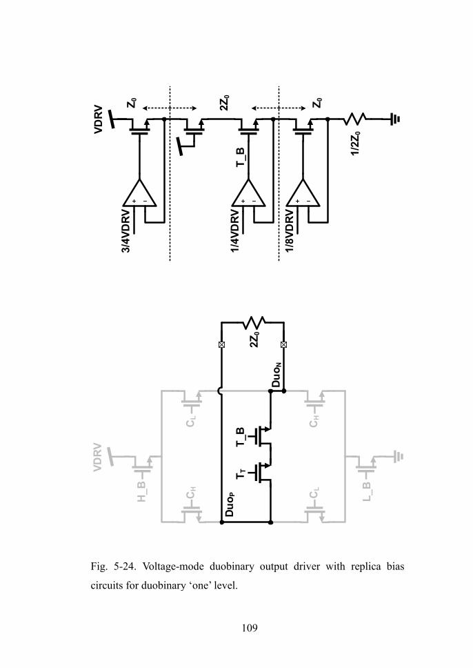
109
TT
T_B
CH
CL
CL
CH
H_B
L_B
VD
RV
Du
oP
Du
oN
2Z
0
T_B
3/4
VD
RV
VD
RV
1/4
VD
RV
1/8
VD
RV
1/2
Z0
Z0
2Z
0
Z0
Fig. 5-24. Voltage-mode duobinary output driver with replica bias
circuits for duobinary ‘one’ level.

110
5.2.4. Phase Calibration with Toggle Signals
Differential or quadrature phase mismatch in the clock can directly
degrade the signal quality and generate ISI at the serialized data.
Moreover, in our consecutive serializer, there is no phase align after data
aligner resulting in phase mismatch get worse. For phase calibration, we
use training sequence before data transmission. As the consecutive high
and consecutive low signals inherently cannot have adjacent data, we
cannot directly get the phase relation information between 0 degree and
90 degree from consecutive signals. However, the positive toggle signal
and negative toggle signal can be generated as adjacent data so that using
toggle signal we can get the phase relation information between 0 degree
and 90 degree or 0 degree and 180 degree. With ‘110011001100…’
training sequence, we can get the positive toggle signal and negative
toggle signal as shown in Fig. 5-25 (a). If we can generate ideal TP,180,
which is 180 degree phase shifted signal of TP, we can calibrate
differential phase by phase matching of TN to the TP,180. For quadrature
phase calibration, we can get the positive toggle signal and negative
toggle signal as shown in Fig. 5-25 (b) with ‘100010001000…’ training
sequence. If we can generate ideal TP,90, which is 90 degree phase shifted
signal of TP, we can calibrate quadrature phase by phase matching of TN
111
to the TP,90.
Fig. 5-26 and Fig. 5-27 show the differential phase calibration block
diagram and quadrature phase calibration block diagram, respectively.
Calibration operation is performed by two steps. First, 180 degree or 90
degree shifted TP signals are generated from digital DLL (delay-locked
loop). Second, phase of TN signal is matched to generated TP,90 or TP,180
resulting in phase calibration. To detect small phase mismatch, PDC
(phase decision circuit) is used which consists of SR-Latch, delay buffer,
and gated D-flip-flop as shown in Fig. 5-28. Dummy blocks are used in
input node of PDC block and output node of SR-Latch for accurate
operation. Fig. 5-29 shows simulation results of locking behavior of
phase calibration block.

112
TP
TN
TP,180
0 90 180 270 0 90 180 270 0 90 180 270
(a)
TP
TP,90
TN
0 90 180 270 0 90 180 270 0 90 180 270
(b)
Fig. 5-25. Training toggle signal sequence for differential (a) and
quadrature phase calibration (b).

113
D0
D36
0
To
gg
le 0
To
gg
le 1
80
D18
0
D18
0
5-b
it
3-b
it
En
DL
L,H
clk
En
CA
L,H
clk
Cal H
DC
DL
PF
D
PF
DP
DC
PD
CU
P/D
N
Co
un
ter
UP
/DN
Co
un
ter
Fig. 5-26. Block diagram of differential phase calibration.

114
D0
D36
0
To
gg
le 0
To
gg
le 9
0
D90
D90
5-b
it
3-b
it
En
DL
L,Q
clk
En
CA
L,Q
clk
Cal Q
DC
DL
PF
DP
DC
UP
/DN
Co
un
ter
UP
/DN
Co
un
ter
PD
CP
FD
Fig. 5-27. Block diagram of quadrature phase calibration.
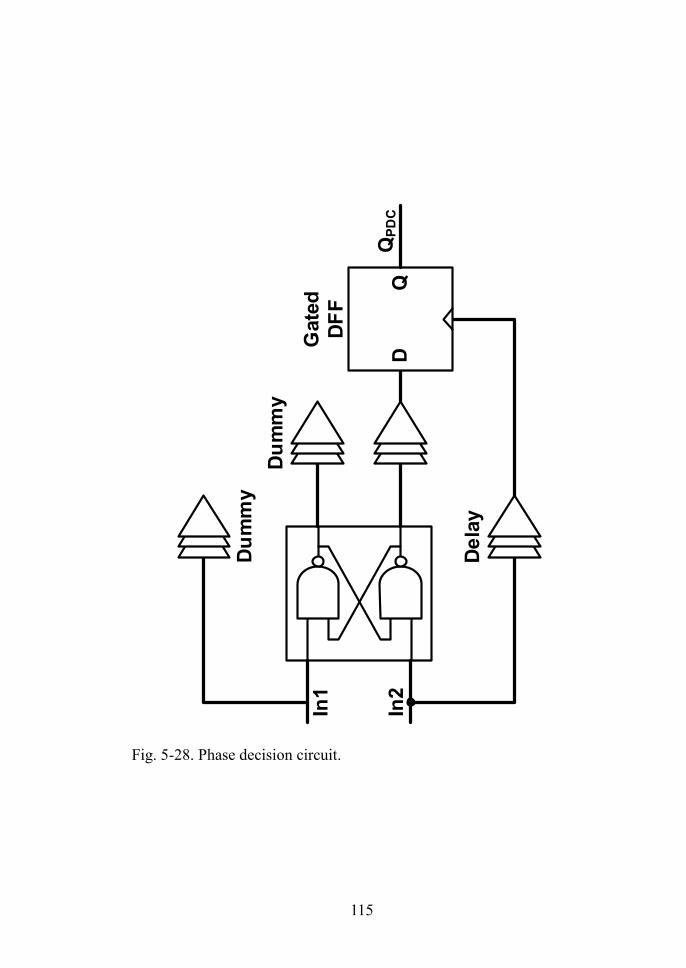
115
Fig. 5-28. Phase decision circuit.

116
Fig. 5-29. Simulation results of phase calibration block.

117
5.2.5. Implementation and Measurement Results
Total transmitter block diagram with consecutive serializer is shown
in Fig. 5-30. The transmitter uses toggle generator for phase calibration
which is turn off after initial phase calibration. As the consecutive signal
generation block and toggle signal generation block have same structure
without parallel input data connection, we can use only one serializer for
consecutive or toggle signal generation. For data connection selection,
data select block is added between RZ data aligner and serializer. From
the (2-1), (2-2), (5-1), and (5-2), we can make data select block with
simple inverter with switch. A prototype duobinary transmitter with
consecutive serializer is fabricated in 28-nm CMOS technology. Fig. 5-
31 shows the microphotograph of the fabricated chip. The active chip
area of duobinary transmitter is 275 × 196 μm2 with an on-chip 27–1
PRBS generator and phase calibration circuits. The transmitter chip
contains I2C (Inter-Integrated Circuit) for digital bit control. The
fabricated chip are mounted on FR 4 PCB and only supply and DC pins
are wire-bonded. DUT is measured by on-board proving for high-speed
input clock and output data.
Fig. 5-32 shows the measured duobinary transmitter output eye
diagram at 12.5, 20, and 25 Gb/s. The differential peak-to-peak voltage

118
is 300 mVppd and output eye diagram have minimum 20 ps width and 45
mVppd height opening which indicate 0.5 UI and 0.6 UI opening at 25
Gb/s, respectively.
Fig. 5-33 shows transmitter output eye diagram with and without
phase calibration at 20 Gb/s and 25 Gb/s. Without phase calibration, eye
openings are different at each eye. However, with phase calibration,
difference of eye openings is greatly reduced. The measurement results
verify our phase calibration circuit. Table 5-7 shows the performance
summary of duobinary transmitter with consecutive signals and
comparison with other duobinary transmitters.

119
Fig. 5-30. Block diagram of duobinary transmitter with consecutive
signals.

120
Fig. 5-31. Chip microphotograph.
196μm
275μm
CA
B
D
E
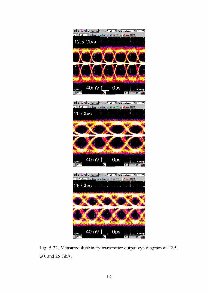
121
12.5 Gb/s
40mV 50ps
20 Gb/s
40mV 20ps
25 Gb/s
40mV 20ps
Fig. 5-32. Measured duobinary transmitter output eye diagram at 12.5,
20, and 25 Gb/s.
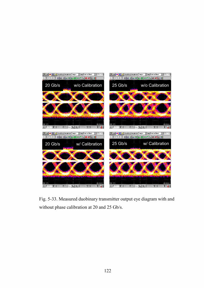
122
20 Gb/s w/o Calibration 25 Gb/s w/o Calibration
w/ Calibration20 Gb/s w/ Calibration25 Gb/s
Fig. 5-33. Measured duobinary transmitter output eye diagram with and
without phase calibration at 20 and 25 Gb/s.

123
TABLE 5-7
PERFORMANCE SUMMARY OF DUOBINARY TRANSMITTER
[20]
[24]
[21]
This
work
Techno
logy
90 n
m28 n
m65 n
m28 n
m
Supply
Voltage (
V)
1.5
0.9
11.2
Data
Rate
(G
b/s
)20
32
4.5
25
Outp
ut S
win
g (
mV
pp,d)
200
120
60
100-3
00
Min
imum
Eye O
penin
g (
UI)
[Data
Rate
]
Wid
th: 0.1
75*
Heig
ht:
N/A
[20 G
b/s
]
Wid
th: 0.5
**
Heig
ht:
0.3
**
[32 G
b/s
]
Wid
th: 0.1
67
Heig
ht:
N/A
[4.5
Gb/s
]
Wid
th: 0.5
Heig
ht:
0.6
[25 G
b/s
]
Pow
er
Consum
ption (
mW
)
[Data
Rate
, S
win
g V
oltage]
120
[20 G
b/s
, 200
mV
pp,d]
97.9
[32 G
b/s
, 120
mV
pp,d]
0.5
4**
*
[4.5
Gb/s
, 60
mV
pp,d]
9.1
5
[25 G
b/s
, 250
mV
pp,d]
Energ
y E
ffic
iency (
pJ/b
it)
[Data
Rate
, S
win
g V
oltage]
6
[20 G
b/s
, 200
mV
pp,d]
3.0
6
[32 G
b/s
, 120
mV
pp,d]
0.1
2**
*
[4.5
Gb/s
, 60
mV
pp,d]
0.3
66
[25 G
b/s
, 250
mV
pp,d]
* A
fte
r 4
0-c
m R
oge
rs b
oa
rd c
ha
nn
el
** A
fte
r -3
dB
loss c
ha
nn
el w
ith
pre
-em
pha
sis
***
Po
we
r co
nsu
mptio
n o
nly
fo
r p
re-d
rive
r a
nd
ou
tpu
t d
rive
r

124
6. Conclusion
In this dissertation, we propose a novel low-power transmitter based
on data transition information. The main motivation is using data
transition information for serialization to avoid short pulse generation.
The power can be saved eliminating the pulse generator and clock buffers
for serialization. Our transmitter extracts the data transition information
from input parallel data, and uses it rather than clock for serialization. In
addition, the data transition information can be used directly for the pre-
emphasis. This can eliminate the use of sub-blocks for generation of 1-
bit delayed sequence. As the serialized output data is highest data-rate in
transmitter, elimination of the blocks for 1-bit delayed data can lead
much of power saving.
As the low-power transmitter verification, we implement 5–8 Gb/s
transmitter with 2-tap pre-emphasis in 65nm CMOS technology.
Dynamic power consumption of our transmitter is analyzed and
compared with conventional transmitter by simulation in 65nm CMOS.
Our transmitter is tested with 27–1 PRBS data from the on-chip generator.
Our transmitter successfully demonstrated 5–8 Gb/s data generation and
transmission through 40-cm PCB channel. With 2-tap pre-emphasis
using toggle signals, low-pass filtering characteristic of channel is

125
compensated and output eyes are more opened. The power consumption
and energy efficiency is compared with other low-power transmitters.
Our transmitter shows the best energy efficiency and further great energy
efficiency with pre-emphasis, which shows the effect of using data
transition information for serialization and pre-emphasis.
Low-power transmitter using data transition information is extended
to the duobinary signaling. By using data transition information,
duobinary generation function, 1 + 𝑍−1 , can be easily performed
without any additional blocks. 5–8 Gb/s and 25 Gb/s duobinary
transmitters are implemented with toggle signals and consecutive signals
in 65nm and 28 nm CMOS technology, respectively.

126
Bibliography
[1] Behzad Razavi, Design of integrated circuits for optical
communications, 2nd ed. New York, NY, USA: Wiley, 2012.
[2] Hungwen Lu, and Chauchin Su, “A 1.25 to 5 Gbps LVDS Transmitter
with a Novel Multi-Phase Tree-Type Multiplexer” in proc. IEEE
Asian Solid-State Circuits Conf. (ASSCC), Nov. 2008, pp. 389-392.
[3] Timothy O. Dickson et al., “A 1.8-pJ/bit 16x16-Gb/s source
synchronous parallel interface in 32nm SOI CMOS with receiver
redundancy for link recalibration” IEEE Custom Integrated Circuits
Conf. (CICC), pp. 1-4, Sept 2015.
[4] Y. Lu et al., “Design and analysis of energy-efficient reconfigurable
pre-emphasis voltage-mode transmitter,” IEEE J. Solid-State
Circuits, vol. 48, no. 8, pp. 1898–1909, Aug. 2013.
[5] Y.-H. Song et al., “A 0.47–0.66 pJ/bit, 4.8–8 Gb/s I/O transceiver in
65 nm CMOS,” IEEE J. Solid-State Circuits, vol. 48, no. 5, pp. 1276–
1289, May 2013.
[6] W.-S. Choi et al., “A 0.45-to-0.7V 1-to-6Gbps 0.29-to-0.58pJpb
Source-Synchronous Transceiver Using Automatic Phase
Calibration in 65nm CMOS,” in IEEE Int. Solid-State Circuits Conf.
(ISSCC) Dig. Tech. Papers, 2015, pp. 66–67.
[7] Y.-H. Song et al., “An 8-to-16Gb/s 0.65-to-1.05 pJ/b 2-tap
impedance-modulated voltage-mode transmitter with fast power-
state transitioning in 65 nm CMOS,” in IEEE Int. Solid-State Circuits
Conf. (ISSCC) Dig. Tech. Papers, 2014, pp. 446–447.
[8] J. Kaukovuori, K. Stadius, J. Ryynänen, and K. A. I. Halonen,
“Analysis and design of passive polyphase filters,” IEEE Trans.

127
Circuits Syst. I, Reg. Papers, vol. 55, no. 10, pp. 3023–3037, Nov.
2008.
[9] Y.-H. Song and S. Palermo, “A 6-Gbit/s hybrid voltage-mode
transmitter with current-mode equalization in 90-nm CMOS,” IEEE
Trans. Circuits Syst. II, vol. 59, no. 8, pp. 491–495, Aug. 2012.
[10] K.-L.Wong et al., “A 27-mW3.6-Gb/s I/O transceiver,” IEEE J.
Solid-State Circuits, vol. 39, no. 4, pp. 602–612, Apr. 2004.
[11] R. Sredojevic and V. Stojanovic, “Fully digital transmit equalizer
with dynamic impedance modulation,” IEEE J. Solid-State Circuits,
vol. 46, no. 8, pp. 1857–1869, Aug. 2011.
[12] K. Fukuda et al., “A 12.3 mW12.5 Gb/s complete transceiver in 65
nm CMOS,” in IEEE Int. Solid-State Circuits Conf. (ISSCC) Dig.
Tech. Papers, 2010, pp. 368–369.
[13] A. Lender, “The duobinary technique for high-speed data
transmission,” IEEE Trans. Commun. Electron., vol. 82, pp. 214–218,
May 1963.
[14] J. H. Sinsky et al., “High-speed electrical backplane transmission
using duobinary signaling,” IEEE Trans. Microw. Theory Tech., vol.
53, no. 1, pp. 152–160, Jan. 2005.
[15] K. Yamaguchi et al., “12 Gb/s duobinary signaling with x 2
oversampled edge equalization,” in IEEE Int. Solid-State Circuits
Conf. (ISSCC) Dig. Tech. Papers, 2005, pp. 70–71.
[16] J. Sinsky et al., “10 Gb/s duobinary signaling over electrical
backplanes–Experimental results and discussion,” Lucent
Technologies, Bell Labs [Online]. Available:
http://www.ieee802.org/3/ap/public/jul04/sinsky_01_0704.pdf
[17] K. Gharibdoust, A. Tajalli, and Y. Leblebici, “A 7.5 mW 7.5 Gb/s
mixed NRZ/multi-tone serial-data transceiver for multi-drop
128
memory interfaces in 40nm CMOS,” in IEEE Int. Solid-State
Circuits Conf. (ISSCC) Dig. Tech. Papers, Feb. 2015, pp. 180–181.
[18] F. Stremler, Introduction to Communication System, 3rd ed. Reading,
MA: Addison-Wesley, 1990.
[19] J. Lee, “A 20Gb/s Duobinary Transceiver in 90nm CMOS,” in IEEE
Int. Solid-State Circuits Conf. (ISSCC) Dig. Tech. Papers, pp. 102-
599, Feb. 2008.
[20] J. Lee, M.-S. Chen, and H.-D. Wang, “Design and comparison of
three 20-gb/s backplane transceivers for duobinary, PAM4, and NRZ
data,” IEEE J. Solid-State Circuits, vol. 43, no. 9, pp. 2120–2133,
Sep. 2008.
[21] S.-M. Lee et al., “An 80 mV-swing single-ended duobinary
transceiver with a TIA RX termination for the point-to-point DRAM
interface,” IEEE J. Solid-State Circuits, vol. 49, no. 11, pp. 2618–
2630, Nov. 2014.
[22] H.-W. Lim et al., “A 5.8 Gb/s adaptive integrating duobinary based
DFE receiver for multi-drop memory interface,” in IEEE Int. Solid-
State Circuits Conf. (ISSCC) Dig. Tech. Papers, Feb. 2015, pp. 1–3.
[23] K. Sunaga, H. Sugita, K. Yamaguchi, and K. Suzuki, “An 18 Gb/s
duobinary receiver with a CDR-assisted DFE,” in IEEE Int. Solid-
State Circuits Conf. (ISSCC) Dig. Tech. Papers, Feb. 2009, pp. 274–
275.
[24] Y. Ogata, Y. Hidaka, and Y. Koyanagi et al., “32 Gb/s 28 nm CMOS
time-interleaved transmitter compatible with NRZ receiver with
DFE,” in IEEE Int. Solid-State Circuits Conf. (ISSCC) Dig. Tech.
Papers, 2013, pp. 40–41.

129
List of Publications
International Journal Papers
[1] Sung-Geun Kim, Jinsoo Rhim, Dae-Hyun Kwon, Min-Hyeong Kim,
and Woo-Young Choi, “A Low-Voltage PLL with a Supply-Noise
Compensated Feedforward Ring VCO,” IEEE Trans. Circuits Syst.
II, Exp.Briefs, Vol. 16, No. 3, pp. 548-552, June 2016.
[2] Kwang-Chun Choi, Sung-Geun Kim, Seung-Woo Lee, Bhum-Cheol
Lee, and Woo-Young Choi, “A 990-μW 1.6-GHz PLL Based on a
Novel Supply-Regulated Active-Loop-Filter VCO,” IEEE Trans.
Circuits Syst. II, Exp.Briefs, Vol. 60, No. 6, pp. 311-315, June 2013.
130
International Conference Presentations
[1] Sung-Geun Kim, Tongsung Kim, Dae-Hyun Kwon, and Woo-
Young Choi, “A 5-8 Gb/s Low-Power Transmitter with 2-Tap Pre-
Emphasis Based on Toggling Serialization,” in proceedings of Asian
Solid-State Circuits Conference (ASSCC) (2016).
[2] Sung-Geun Kim, Jinsoo Rhim, Dae-Hyun Kwon, Min-Hyeong Kim,
and Woo-Young Choi, “A Low-Voltage PLL with a Current
Mismatch Compensated Charge Pump,” in proceedings of IEEE
International SoC Design Conference (ISOCC) (2015).
[3] Joung-Wook Moon, Sung-Geun Kim, Dae-Hyun Kwon, and Woo-
Young Choi, “A 0.4-V, 500-MHz, Ultra-Low-Power Phase-Locked
Loop for Near-Threshold Voltage Operation,” in proceedings of
IEEE Custom Integrated Circuits Conference (CICC) (2014).
[4] Jaeseok Park, Ingeol Lee, Young-Seok Park, Sung-Geun Kim,
Kyung Ho Ryu, Dong-Hoon Jung, Kangwook Jo Choong Keun Lee,
Hongil Yoon, Seong-Ook Jung, Woo-Young Choi, Sungho Kang,
“Integration of dual channel timing formatter system for high speed
memory test equipment,” in proceedings of IEEE International SoC
Design Conference (ISOCC) (2012).

131
Domestic Conference Presentations
[1] 임진수, 김성근, 최우영, “65-nm 표준 CMOS 공정을 사용한
25-Gb/s 광 통신용 송신기 회로 설계, 2014년 SoC
춘계학술대회, May 2014, 서울.
[2] 김성근, 최우영, “MASH 델타 시그마 모듈레이터의 스퍼
제거에 관한 기술 연구,” 2011 SoC 학술대회, Apr. 2011, 충북.

132
Patents
[1] Sung-Geun Kim, and Woo-Young Choi, “Serializer and Data
Transmitter Comprising the Same,” USA Patent (Registered), Patent
No. 9685978, June. 20, 2017.
[2] Sung-Geun Kim, and Woo-Young Choi, “Voltage Controlled
Oscillator and Phase Locked Loop Comprising The Same,” Korean
Patent (Registered), Patent No. 10-1704711, Fab. 02, 2017.
[3] Sung-Geun Kim, and Woo-Young Choi, “Voltage Controlled
Oscillator and Phase Locked Loop Comprising The Same,” USA
Patent (Pending), Application No. 15/376,346, Dec. 12, 2016.
[4] Sung-Geun Kim, and Woo-Young Choi, “Serializer and Data
Transmitter Comprising the Same,” CHN Patent (Pending),
Application No. 2015109189437, Dec. 15, 2015.
[5] Sung-Geun Kim, and Woo-Young Choi, “Serializer and Data
Transmitter Comprising the Same,” Korea Patent (Registered),
Patent No. 10-1543704, Aug. 05, 2015.