Embed Size (px)
Citation preview

Summary Descriptions of Selected Projects Being Investigated (Sungho Jin and collaborators)
Si Nano/Micro-Shaping for Reduced Cost Photovoltaic Solar Cells
1. Low cost Si slicing for photovoltaic cells [Drastically reduced kerf loss]2. Thermoelectric materials [Easy scale-up manufacturing of nano-grained TE
materials.] 3. Wear-resistant, self-cleaning, superhydrophobic coatings [Ceramic based,
teflon-free, inexpensive and durable super-omniphobic coatings on glass, plastic and other surfaces]
4. Concentrating solar power (CSP) system, solar-thermal generator [Spectrally selective, sunlight-absorbing coatings]
5. Dye sensitized solar cells (DSSC) and perovskite sensitized solar cells (PSSC) [FTO glass free, transparent and high-electrical-conductivity electrodes]
6. Compliant thermal interface material (TIM) [To provide mechanical stress accommmodation and high thermal conductivity simultaneously]
7. 7. Ultra-high-density vertical solar cell array [DUV processed or nano-imprinted Si]
8. Sunlight reflective coatings [To keep buildings and automobiles cooler in the summer and warmer in the winter]
9. Universal solders [For easy integration of solar cells involving difficult-to-bond surfaces like Ag-free metallic electrode surface]
Solar Energy Related Technologies R&D (2010 – now)--- Innovative approaches to solve some major problems

Thermoelectric Materials --- The thermoelectric figure of merit (ZT) can be expressed as ZT = (S2σ/k)T (where S is the Seebeck Coefficient, σ is the electrical conductivity, and k is the thermal conductivity. For higher ZT, these materials parameters need to be optimized. --- Thermoelectric (TE) alloys such as Bi-Sb-Te and skutterudites are promising energy materials for waste heat recovery and solar energy generation. For enhanced TE properties such as the energy conversion efficiency, it is essential to increase the phonon scattering and reduce the thermal conductivity. Various nanoparticle synthesis techniques based on physical, chemical or mechanical approaches are utilized to produce variety of nanoparticles of thermoelectric alloys and sintered nanograined alloys having excellent thermoelectric properties. Further nanostructure controls are being investigated to increase the phonon scattering, Seebeck Coefficient, and electrical conductivity of various thermoelectric materials.
(a)(b) (d)(c)
Si waferPR PR PR PR
Magnet
PR
Si waferPR PR PR PR
Sliced Si eetsthin sh
PR PR PR
H
Schemati ss. (a) Photores netic catalyst la 00 parallel etch lines ) Magneticguided el Au catalyst removal
cs of the magnetically direction-guided, catalytic silicon slicing proceist line pattern on Si ingot surface using photolithography, (b) Mag
yer deposition (5-20 μm wide and 5-20 μm spaced apart, up to 20,0 over 20 cm length Si ingot) for massively parallel Si wafer slicing, (cectroless etching into Si depth, (d) photoresist lift-off and remaining
to obtain thin microsheets of sliced Si.
Thin sliced Si ribbons, pillars, bent nanowires by catalytic shaping
~20 μm thick x 200 μm tall Si sheets on Si base
5~10 μm dia. x ~200 μm tall Si micro pillar array on Si base
25 μmSi base
~20 μm
(a) (b)
Si base
5 μm700 nm dia. Bent Si NW
500 nm
(d)
300 nm dia. zig-zag Si NW
(c)
(a) SEM Image of Bi-Sb-Te thermoelectric allot nanoparticleswith ~30nm dia., (b) TEM of spark plasma sintered (SPS) Bi-Sb-Te thermoelectric alloy with desirable nanograin structure for enhanced phonon scattering.
20 nm100 nm
(a) (b)

--- Wear resistant, superhydrophobic glass surface made of transparent ceramic nanostructure, rather than easily smearablepolymer coatings. Such coatings are needed for many industrial and consumer market applications. --- For anti-fingerprint surface (on cell phones or touch-sensitive screens), both superhydrophobic + superoleophobic properties are needed.--- Also, for “maintenance-free, antir-eflective PV cell array and clean high-rise-building window glasses.--- Such transparent ceramic coatings have been developed (past 5 yrs R&D effort), and scale-up manufacturability is being considered in the nanostructure design and processing.
300 350 400 450 500 5500.0
0.5
1.0
1.5
2.0
Latti
ce th
erm
al c
ondu
ctiv
ity (W
/mK
)Temperature, T(K)
demo
Spark eroded powder, SPS@450CIngot(Bi0.5Sb1.5Te3)Milled powder, SPS@450C
Lattice thermal conductivityNanograined alloy,
300 350 400 450 500 5500
50
100
150
200
250
300
Seeb
eck
coef
ficie
nt, S
(µV
/K)
Temperature, T(K)
Spark eroded powder, SPS@450CIngot(Bi0.5Sb1.5Te3)Milled powder, SPS@450C
Nanograined alloy
Seebeck coefficient
300 350 400 450 500 5500.0
0.3
0.6
0.9
1.2
1.5
Figu
re o
f mer
it, Z
T
Temperature, T(K)
Spark eroded powder, SPS@450CIngot(Bi0.5Sb1.5Te3)Milled powder, SPS@450C
ZT vs Temp plot
Nanograined alloy,
(a) Seebeck coefficient, (b) Lattice thermal conductivity and (c) ZT, vs measurement temp of Bi-Sb-Te thermoelectric alloy after spark plasma sintering.
Vapor
Liquid
Solid
γLV
γSL
γSVθc
(a) Hydrophilic (b) Hydrophobic (c) superhydrophobic
θc
Self-Cleaning Surface --- water nonwetting & oil nonwetting are
θc
necessary conditions.
--- Schematic illustration of contact angles for hydrophilic,hydrophobic, and superhydrophobic surfaces. A similar definition of oleophilic, oleophobic and superoleophobic, also applies for oil wetting instead of water wetting. --- Super-omniphobic ceramic surface (having both superhydrophobic and superoleophobic) has been demonstrated.
Self-cleaning glass surface--- Nanostructured glass or silica surfaces having superhydrophobic and omniphobic properties have been developed for maintenance-free solar panel surface (with minimal needs for washing/cleaning during solar cell use lifetime).
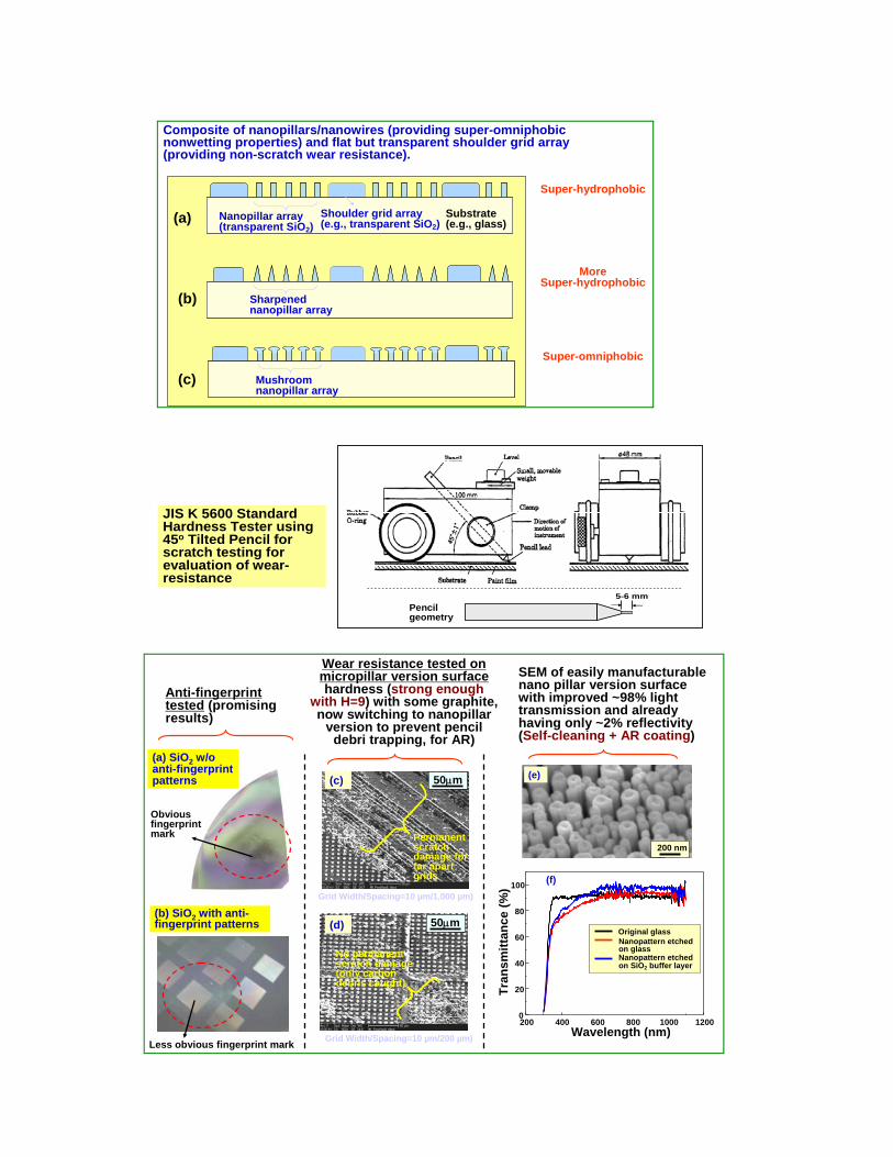
Composite of nanopillars/nanowires (providing super-omniphobicnonwetting properties) and flat but transparent shoulder grid array (providing non-scratch wear resistance).
(a)
(b)
Nanopillar array (transparent SiO2)
Shoulder grid array (e.g., transparent SiO2)
Substrate (e.g., glass)
(c)
Sharpened nanopillar array
Mushroom nanopillar array
Super-hydrophob
More Super-hydrophob
ic
ic
Super-omniphobic
JIS K 5600 Standard Hardness Tester using 45o Tilted Pencil for scratch testing for evaluation of wear-resistance
Pencil geometry
5-6 mm
Wear resistance tested on
Obvious fingerprint mark
(a) SiO2 w/o anti-fingerprint patterns
Less obvious fingerprint mark
(b) SiO2 with anti-fingerprint patterns
Grid Width/Spacing=10 µm/200 µm)
Grid Width/Spacing=10 µm/1,000 µm)
50μm (c)
50μm (d)
Permanent scratch damage for far apart grids
No permanent scratch damage (only carbon debris caught)
200 400 600 800 1000 12000
20
40
60
80
100
Tran
smitt
ance
(%)
Wavelength (nm)
Original glassNanopattern etched on glassNanopattern etched on SiO2 buffer layer
200 nm
(e)
(f)
Anti-fingerprint micropillar version surface
tested (promising results)
hardness (strong enough with H=9) with some graphite, now switching to nanopillar
version to prevent pencil debri trapping, for AR)
SEM of easily manufacturablenano pillar version surface with improved ~98% light transmission and already having only ~2% reflectivity (Self-cleaning + AR coating)

Concentrating Solar Power --- High Performance Nanostructured
Spectrally Selective Coating
• Concentrating solar power (CSP) --- A viable, commercialized technology that competes effectively with the photovoltaic solar energy. This Carnot cycle based energy conversion is based on focusing sunlight onto the Spectrally Selective Coating (SSC) on a steel pipe that contains a molten salt heated by the absorbed thermal energy. The molten salt is sent to the power plant where steam is generated to operate steam turbines and generate electricity. The solar thermal Carnot cycle efficiency is high, ~40% at the current operating temperature of ~450oC. the goal of this DOE-funded project is to further increase the efficiency toward ~60% regime by developing new, more efficient, sunlight absorbing SSC layer that will enable a 700-750oC CSP operation. These efficiency values are much higher than the typical photovoltaic energy conversion efficiency (~25%).
• Spectrally selective coating (SSC) --- A critical component that enables high-temperature and high-efficiency operation of concentrated solar power (CSP) systems. SSC has a profound impact on the performance and cost of CSP systems. The optical properties of the SSC, namely, absorption in the solar spectrum range (UV/Vis) is maximized by materials design as we pursue a bandgap-adjusted, nanoparticle semiconductor materials while the reflectance, while the undesirable black body emission loss in IR (infrared) regime is minimized.
• For higher temperature operation to achieve higher Carnot efficiency, the semiconductor material nanoparticles need to be p , e.g., with the synthesis of a variety of nano tures. configuration surface layer as investigated in this project.
rotected from oxidation core-shell struc

Rare-Earth-Free Permanent Magnet Alloys --- The high price of rare earth metals, especially Dy utilized in Nd-Fe-B magnets has instigated active R&D toward new, rare-earth-free permanent magnet materials. --- We employ a spark erosion technique to easily produce nanoparticles of Mn-Bi magnet alloys so that the high magnetocrystalline anisotropy of the material is fully utilized with minimal domain wall motion. Soft-magnet / hard-magnet exchange coupled spring magnets with higher coercive force are also being developed.
Spark erosion principle for nanoparticle synthesis. Smell-O-Vision Devices Using X-Y Matrix Controlled Odor Release
50 nm
TEM of spherical, single domain MnBi particles (d<30 nm).
--- Virtual reality can be made more realistic with a three-dimensional or other sensory input. Out of the five senses humans have (i.e., vision, sound, smell, taste and touching), we have already incorporated the first two senses in modern communications and entertainment systems such as TVs, mobile phones, computers, and movies. --- To enhance the quality of entertainment and communications, it would be nice to incorporate another sense, a sense of smell. Synchronization of odor release to the corresponding image on the screen can be accomplished conveniently by electronic signals using a reliable, inexpensive, and not cumbersome device. --- Odor releasing devices that allow easy on-off switching of odor flux could have a significant impact on the effectiveness of virtual reality. We have developed a fast, repeatable new odor/gas releasing system having a novel X–Y matrix addressable
Hc vs Temp. for spark eroded MnBinanoparticles--- Hc approaching 30 KOe--- The stability of Hc well beyond 200oC, up to ~300oC (573K) demonstrated.--- Exchange coupled core-shell magnets being designed.
300 360 400 440 480 520 560 600 640 680 7200
10
20
30
Hc
(KO
e)
Temp (K)
Hc(minor loops)Hc(hypoth.
major loops)
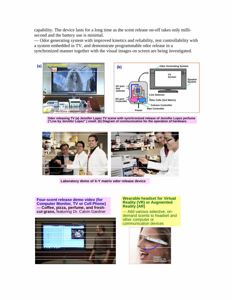
capability. The device lasts for a long time as the scent release on-off takes only milli-second and the battery use is minimal. --- Odor generating system with improved kinetics and reliability, test controllability with a system embedded in TV, and demonstrate programmable odor release in a synchronized manner together with the visual images on screen are being investigated.
Four-scent release demo video (for Computer Monitor, TV or Cell Phone) --- Coffee, pizza, perfume, and fresh-cut grass, featuring Dr. Calvin Gardner
Hinged armature for scent release
Wearable headset for Virtual Reality (VR) or Augmented Reality (AR)--- Add various selective, on-demand scents to headset and other computer or communication devices
Laboratory demo of X-Y matrix odor release device
Odor Cells (3x3 Matrix)
Line Selector
Speaker System
Odor Generating System
Column ControllerRaw ControllerPower
I/O portline selector
I/O portController
TV Screen
Odor releasi(“Li
ng TV (a) Jennifer Lopez TV scene with synchronized release of Jennifer Lopez perfume ve by Jennifer Lopez” ) smell. (b) Diagram of communication for the operation of hardware.
(b)TV screenOdor generator
Perfume odor test apparatus
(a)

----------------------
Graphene Processing and Properties
Headset Prototype Demo (VR Images + 6 Scents release) video
Communications/entertainments/VR-AR--- Virtual Reality/Augmented Reality, Computer Monitors, Smell-o-Vision TVs
(+ commercials, movies, perfume stores), games.--- Odor release cell phones.--- Advertizing products, smell-able food display, home and personal items. --- Cars/autonomous cars, airplanes, homes, businesses, etc.--- On-Line-Shopping devices for many personal computers in the world.
Medical applications--- Combinatorial synthesis /discovery of vapor-based new drugs.--- Release of medical vapors or nano-mists in arrays or in mixtures. This can allow to overcome the Blood-Brain-Barrier problem to enable delivery ofAlzheimer’s Disease drug or Parkinson’s Disease drug to brain cells.
Security devices (for homeland security, military, civilian) (a) Remote release of neutralizing/decontaminant gas in the event of
terrorist attack with toxic gas (e.g., in subway station)(b) Capturing of enemy solders or intruders by releasing
sedative/anesthesia gases or laughing gas (e.g., nitrous oxide). (c) Wearable gas release on soldiers uniform.(d) Remotely controllable release of pungent foul smell like skunk smell to
chase away intruders.
Potential Applications of Scent Release Devices---Technology has been demonstrated and is ready for commercialization.
Graphene is a very exciting new material with many potential applications. For semiconductor use with graphene’s high carrier mobility and other unique properties, the band-gap has to be opened.New Anodized Aluminum Oxide (AAO) template with smaller 40-50 nm dia
pores, 200-300nm thickness developed. Such AAO templates were utilized to pattern graphene layer (CVD grown
on Cu substrate followed by removal of Cu). Honeycomb-geometry graphene was obtained so as to produce enhanced edge effect and band-gap opening. Magnetic nano-island arrays are also being fabricated for enhanced magneto-transport properties.Electronic and magnetic properties of nano-modified graphene layers are
being evaluated.

x13.4x14.9x11.9x13.8
x13.5x17.4
30 sec 40 sec 50 sec
0.0
5.0x10 3
1.0x10 4
1.5x10 4
2.0x10 4
2.5x10 4
3.0x10 4
NPGNPG w/ HNO3Pristine G
Rs(
ohm
/sq)
Etching Time (sec)Sheet resistance (Rs) increase caused by nano-patterning of graphene (green arrows)using AAO template etch mask, and near-complete recovery of the electrical conductivity byHNO3 chemical doping (red arrows), especially for the 40 sec etched graphene sample. The Rsvalues are plotted for three different etching times (30, 40 and 50 sec).
100 nm100 nm 200nm200nm
New AAO template (a) (b)
with smaller pores, (a) top, (b) side view
500nm500nm
(a),(b) Nano-patterned graphenelayer, (c) Ni nanoparticle attached graphene
100nm
(a) (b) Nano poin graph
res ene (c)
Ni nanoislands
200 nm

---------------- Carbon Nanotube Geometry Control
UV–VIS spectra of pristine and nano patterned (NP) graphene films onquartz substrates, showing a significant increase of optical transmissionby nano-patterning.
400 500 600 700 80070
75
80
85
90
95
100
Pristine G NPG (40 s) w/ HNO3
PG w/ HNO3
NPG (30 s) w/ HNO3
Tran
smitt
ance
(%)
Wavelength (nm)
84.9
82.7
97.8
93.9
• Sharply pointed carbon nanotubes can have even smaller tip diameter because of elimination of
catalyst particle radius of curvature. Such sharp tips are advantageous for enhanced field emission, high-resolution metrology, bio-insertion of molecules and functionalities, etc.
• While straight carbon nanotubes are relatively easy to grow, curved or bent nanotubes are difficult to synthesize --- For technical applications, sharply bent or zig-zag carbon nanotubes are important for nano spring applications, sidewall tracing scanning probes, routing of nanoelectronics interconnects, and possible introduction of defects to form hetero-junction nanotube semiconductor devices.
Bending and orienting of Carbon Nanotubes: Experimental Setup and Electric -Field-Direction Modeling
First Growth Stage
Molybdenum Si Substrate
Electric Field Direction (Arrows)
Carbon Nanotubes
Second Growth StageCarbon Nanotubes
Si
Molybdenum
SiliconElectric Field Direction (Arrows)
Molybdenum
Si Substrate Substrate
Molybdenum
ctor modeling done using Maxwell SV
Si
E ve

Perio b
odic and Alig
CVD --- JosDaraio--- Jos Nan Ca beh
• • • •
by Electric-Fined Carbon
D growth ch
seph F. AuBucho, and Sungho seph F. AuBuch
noelectroniarbon nanothavior and l
P. R. BandSharp tranNatural CNThree-way
ield-Guided CNanotube A
hamber for b
hon, Li-Han CJin, Nano Letthon, Li-Han C
ics tubes for nalogic in CNT
daru, C. Darainsistor switchiNT gate --- Noy gating operat
CVD GrowthArray
bent or zig--zag nanotu
Chen, Andrew It. 4, 1781 (200
Chen, and Sung
anoelectroniT Y-Junctioio, S. Jin and Aing behavior eo external gatetion demonstr
I. Gapin, Dong4).
gho Jin, J. Phys
ics --- Electron transistoA. M. Rao, Naenbled by 3rd be fabrication nrated.
Three Step Zigbe growth
g-Zag Structure Five Step Zig--Zag Structure
g-Wook Kim,
500 nm
CChaira
s. Chem. B1099, 6044-6048 (22005).
rical switchiing rs
ature Materialsbranch as a ga
s 4, 663 (2005)). a
necessary. te.
Nan•
• •
•
Carb
High rfilm b
C
A-----
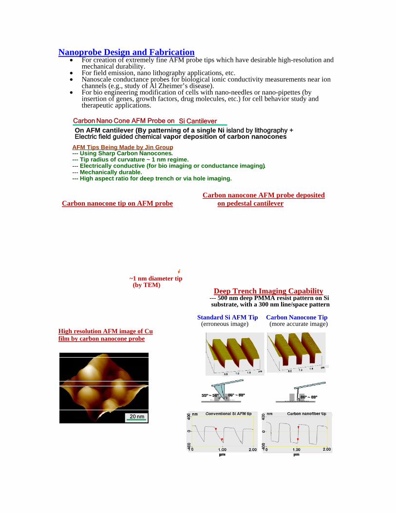
noprobe DeFor creatiomechanicaFor field eNanoscalechannels (eFor bio eninsertion otherapeutic
bon nanocon
resolution AF
by carbon nan
Carbon NanoOn AFM canElectric field
AFM Tips Bein--- Using Shar--- Tip radius o--- Electrically--- Mechanical--- High aspec
esign and on of extremeal durability. mission, nano conductancee.g., study of gineering mo
of genes, growc applications
ne tip on AFM
~1 nm (by TE
FM image of Cocone probe
20 nm
o Cone AFM Pntilever (By guided chem
ng Made by Jrp Carbon Nanof curvature ~
y conductive (lly durable.
ct ratio for dee
Fabricatiely fine AFM
o lithographye probes for bif Al Zheimer’odification of wth factors, drs.
M probe
diameter tipEM)
Cu
Probe on Sipatterning o
mical vapor din Groupnocones.~ 1 nm regime(for bio imagin
ep trench or v
on probe tips wh
y applications,iological ionis disease). cells with nanrug molecules
Carbon on
De --- 50 subs
Standard (erroneo
Cantilever of a single Ndeposition o
e.ng or conduc
via hole imagi
hich have des
, etc. ic conductivit
no-needles ors, etc.) for cel
n nanocone An pedestal ca
eep Trench I00 nm deep PMstrate, with a 3
d Si AFM Tip ous image)
i island by litof carbon na
ctance imagin
ing.
sirable high-re
ty measureme
r nano-pipettell behavior stu
AFM probe dantilever
Imaging CaMMA resist p300 nm line/sp
Carbon Na (more accu
thography + nocones
g).
esolution and
ents near ion
es (by udy and
deposited
apability pattern on Si pace pattern
anocone Tip urate image)
d

Focu--- CN
used Ion Bea
Si na
•
NT with subtraam Modifica
anophotonicFocused-ilocally slsmaller, d
Si bas
E-beam lines to propag
40% Carvinof CNT
90% Carvingof CNT
active line defation of Nan
cs --- For fution-beam calow down ldimensionall
ed waveguide s
m patterned nao intentionallygating optical Be
ng T
g T
Si lindime
fects + four-ponostructure
ture ultra-harved to intrlight movemly optimized
tructure
arrow Si y delay signals fore FIB
Mild shaving
nk wall ension
oint lead wireses
high-densityroduce delayment througd paths.
FIB ma narrow if need
FIB-addedLead Wires
Carving of with Ion Be
Beam Size
1 μm
s for electroniic transport mmeasurements.
CNT eame
y Semiconduy lines for l
uctor circui
gh Si waveg
achining of Si w down the Sided
Afte
Sidewall thinned by FIB
light propagits
guide --- b
to further
i optical path
er FIB
1
ation and ty fabricatin
to ng
μm

Nanofabrication of 10-15 nm features E-beam patterned HSQ resist island array with 1.6 TB/in2 density on Si
Magnetic Nanostructure and Patterned Recording Media • There is a need to substantially increase the density of magnetic
recording media. • Patterned media with periodic array of ~10-20 nm regime magnetic
nanoislands or nanowire magnets are highly desirable. • 0-20 nm nanomagnet dimension is well below the available lithography
limit. • New, innovative synthesis/fabrication approaches are desirable.
Upper Limit Recording Density vs Bit SizeNano-Patterned Perpendicular Recording Media
Bit Size (nm) 2 3 5 10 12.5 15 20(Period, nm) (4) (6) (10) (20) (25) (30) (40)Recording Density (TB/in2) 42 18 6.5 1.6 1.0 0.7 0.4
Bit Size(NanomagnetDiameter)
100 nm
Successfully Fabricated ~20 nm Diameter Vertically aligned CoPtNanomagnets in Anodized Aluminum Oxide Membranes
CoPt nanomagnets(aluminum oxide matrix dissolved away to show the nanowires)

Ener Bio M
E
--w--p
Carb
C
5 μ
a
5 μ
a
Carb--- O--- A
E
Adva
Aligncarbo60 nm
anced Patte
rgy-Relate
Materials
Electrochem
-- The preswith the inte-- Tip-Openarticles (red
CNT
bon Microfiber
Cap (Ni)
μmμm
bon NanotubOn conductive sAs electrode ma
ned and separaton nanotubes (30m dia)
erned Reco
ed Materimical Modif
Na
ence of metended chemning (oxidatduction) on
1) Electrochemicaloxidation
2) Supercritical CO2 drying
Tip-O
be Array for Fsubstrate (carbaterial to carry
ed 0- Carbon m
conducto
ording Med
als fication of Vanotube Ar
tal particlesmical or elect
tion) + electnto verticall
l
Open (Metal Remo
1 μm
b
1 μm
b
Fuel Cell Appon microfiber, caPt catalyst part
microfiberors (~5 μm dia.)
E
dia by Nan
Vertically Arrays
s (e.g., Ni) mtrochemicatrodepositioly-aligned C
3) Electrochemireduction
oved) CNT
4) SupercriticCO2 drying
plicationsarbon paper)ticles
nofabricatio
Aligned Carb
may interferal reactions.on of Pt nanCNT arrays
ical
Pt Nanopartic
al g
2
c
2
c
on
bon
re . no.
cles
00 nm00 nm

Nanotoxicity Study --- Response of PC12 newral cells to magnetic nanoparticles Fe3O4 conc.=15 mM (dramatic reduction of cell ability to generate neurites with increased concentration of of magnetic nanoparticles Fe O conc. = 15 mM --- ~spherical cell shape with much decreased surface area)
Immunofluorescence of typical PC-12 cells 4 days after endocytosis. Cytoskeletal structure shown with tubulin (fluorescein, green) and actin (rhodamine, TRITC labelled phassloidin, red).
3 4
B
10 um
BA
10
A
10 um
10 nm
(c) Fe3O4 Magnetic Nanoparticle Array(a) Superparamagnetic Fe3O4
Examples of Synthesis and Applications of Magnetic NanoparticlesPotential Bio Applications – Cancer treatment, gene delivery, neural regeneration, drug delivery, magnetic cell sorting, MRI.
(b) Silica-Coated Fe3O4
0
10
20
30
40
50
60
70
80
0 200 400 600 800 1000 1200 1400Time of AC Magnetic Heating [sec]
Avg
. Tem
p. [o
C] 1.5 %
0.75 %
0.15 %
3 %
6 % Volume Fraction
Temperature rise induced by remote magnetic field (100 KHz)--- In a liquid containing various volume of magnetic nanoparticles. --- ~10 nm diameter Fe3O4 particles. --- Live cell magnetic hyperthermia experiments to be carried out.
PC-12 Neural Cancer Cells with Endocytosed Magnetic Nanoparticles -- Can be stimulated into Neurite growth by NGF growth factor
45oC
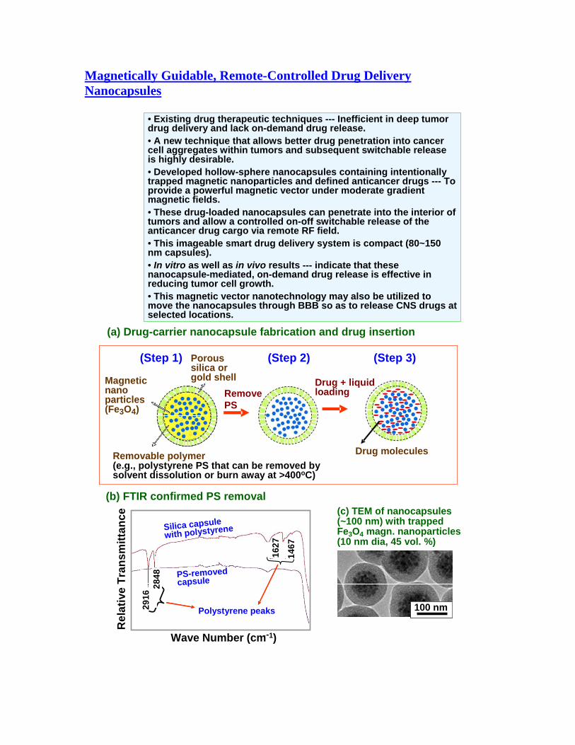
Magnetically Guidable, Remote-Controlled Drug Delivery Nanocapsules
• Existing drug therapeutic techniques --- Inefficient in deep tumor drug delivery and lack on-demand drug release. • A new technique that allows better drug penetration into cancercell aggregates within tumors and subsequent switchable release is highly desirable. • Developed hollow-sphere nanocapsules containing intentionally trapped magnetic nanoparticles and defined anticancer drugs --- To provide a powerful magnetic vector under moderate gradient magnetic fields. • These drug-loaded nanocapsules can penetrate into the interior of tumors and allow a controlled on-off switchable release of the anticancer drug cargo via remote RF field. • This imageable smart drug delivery system is compact (80~150 nm capsules). • In vitro as well as in vivo results --- indicate that these nanocapsule-mediated, on-demand drug release is effective in reducing tumor cell growth. • This magnetic vector nanotechnology may also be utilized to move the nanocapsules through BBB so as to release CNS drugs at selected locations.
(Step 1) (Step 2)
Drug molecules
Remove PS
Porous silica or gold shellMagnetic
nanoparticles (Fe3O4)
(Step 3)
(a) Drug-carrier nanocapsule fabrication and drug insertion
Drug + liquidloading
Removable polymer (e.g., polystyrene PS that can be removed by solvent dissolution or burn away at >400oC)
(b) FTIR confirmed PS removal(c) TEM of nanocapsules(~100 nm) with trapped Fe3O4 magn. nanoparticles(10 nm dia, 45 vol. %)
PS-removed capsule
Silica capsule with polystyrene
Rel
ativ
e Tr
ansm
ittan
ce
Wave Number (cm-1)-
Polystyrene peaks
1627
1467
100 nm
2848
2916
100 nm

(a) Colony penetration (Y-Z section)
50 µm50 µm50 µm50 µm
H
(b) Colony penetration
Control (No field)
Magnet
Control (No field)
Magnet
(X-Y section near the bottom)
FITC/ Phalloidin-TRITC/ DAPI
Confocal microscopy images of the magnetic nanocapsule penetration into MT2 breast cancer cell colony using magnet gradient pulling force (vertical scale bar=50 µm) applied for 2 hrs by a Nd-Fe-B magnet (H=~1,200 Oe near the cancer colony location). The Y-Z vertical section image, and X-Y horizontal section image near the bottom demonstrate a successful penetration of cancer colony by magnetic nanocapsules.
Tissue penetration by magnetic vector
0.0
0.2
0.4
0.6
0.8
OFF*ON**
OFF*ON**OFF*
ON**OFF*
(a)C
ptR
elea
se (n
mol
/mg
NC
s)
RF Magn. Field Cycle Dox
Rel
ease
( nm
ol/m
g N
Cs )
RF Magn. Field ON-Off CycleOFF*
ON**OFF*
ON**OFF*
ON**OFF*
ON**OFF*
0.0
0.4
0.8
1.2
1.6
2.0Remotely switchableon-off drug release by RF magnetic field
(b)
Dox
Rel
ease
( nm
ol/m
g N
Cs )
RF Magn. Field ON-Off CycleOFF*
ON**OFF*
ON**OFF*
ON**OFF*
ON**OFF*
0.0
0.4
0.8
1.2
1.6
2.0Remotely switchableon-off drug release by RF magnetic field
(b)
On-off switchable release from the magnetic nanocapsules. (a) Release of hydrophobic camptothecin (nanomole per mg nanocapsule, NC) by RF magnetic field on-off cycling (switch-on period=10 seconds, switch off=5 minutes), (b) A similar switchable release is demonstrated for hydrophilic doxorubicin from the nanocapsules by RF field.
Hydrophobic drug release (CPT) Hydrophilic drug release (DOX)

UEffec
TiO2~80
Conattanan
Bloo
Ant
ct of Nanost
2 nanotubes onnm dia., 300 nm
nfocal microached + tail vnocapsules (
vessel
d vessel (TRIT
thracene‐Na
tructure of B
Ti --m long
oscopy for Bvein injectio(green). – BB
TC‐dextran, re
noparticle (g
Bio Materia
T
Ti
BB crossingn on mouse
BB crossing
d)
green)
Blo
als on Cell G
Top vi TiO2 n
Ti
O2
g [Polystyree + confocal is observed
Red
ood vessel
Growth
ew TEM micnanotubes
ne surface +microscopy
d.
ve
and green m
Magn nacapsulesaway frovessels
crograph of a
+ fluoresceny to trace ma
v
ssel
merged imag
Scale bar
anos
om
aligned
nt dye agnetic
vessel
ge
r = 50um

UC
EL
TiO2Nan
Control of St
Enhanced OsteoLock-In on Ana
2otubes
Cell G
tem Cell Di
oblast Cell Adhatase TiO2 NanoGrowth into TiO
fferentiatio
hesion and otubesO2 Nanotubes
n Dictated S
Effect oCell GrGrowth
00
200
400
600
800
1000
Num
ber o
f Adh
ered
Cel
ls, 1
03 /cm
2
Soly by Nan
of TiO2 Nanoturowth --- Signh by ~ 300 – 40
10 20
Ti
Incubatio
Heat-treateTiO2 nanot
notube Dim
ube Layer on nificantly Acce00%
30 40on Time (hrs)
ed TiO2 nanotubtubes
ension
Osteoblastlerated
50 60
bes

E Im
FDA and v(24 h
•
•
• SSP--
Effect of Nan
mmunofluor T
images of hvarious diamhr culture, Sc
TiO2 nanmesenchySmaller dproliferanm dia) cpreferentfor ortho
eunghan Ohungho Jin, “
PNAS 106(7)---------------
nostructure
rescent imagTiO2 nanotub
hMSCs on flmeter TiO2 nacale bar=100
notube dimeymal stem cdiameter nation withoucause the stetially differe
opaedic and h, Karla Bram“Stem Cell F), 2130-2135---------------
ed Substrate
ges of reactedbes after 3 w
at Ti anotubes
0 µm).
ension signicell) differenanotubes (~3ut differentiaem cells to sentiate into dental appl
mmer, Julie LFate Dictated5 (2009). ---------------
e on Growth
d stem cellseeks of cultu
ificantly inflntiation beh30 nm dia) eation, whilesubstantiallbone cells (
lications. Li, Dayu Te
d Solely by A
---------------
Ac
Ac
h of Mesenc
on 100nm dure.
luences the havior enhance cele larger diamy elongate, (osteoblasts
eng, Adam EAltered Nano
----------------
ctin
ctin O
O
chymal Stem
diameter
hMSC (hum
ll adhesion ameter nanotstressed and), which can
Engler, Shu Cotube Dimen
----------
Osteocalcin
Osteopontin
m Cells
man
and tubes (~100 d n be useful
Chien, nsion”,
DAPI
DAPI