Embed Size (px)
Citation preview

February 2008 Rev 3 1/21
AN2452Application note
STW8110x evaluation board and graphical user interface
Application and scopeThis application note describes the evaluation board (EVB) and the graphical user interface (GUI) of the STW81101, STW81102 and STW81103 multi-band RF frequency synthesizers (with integrated VCOs).
The STW8110x GUI software allows the STW81101, STW81102 and STW81103 synthesizers to be programmed via an I2C/SPI control interface.
Three evaluation boards are available depending on the output matching network optimal frequency range:
■ EVB1G (single output - 1 GHz - output divider by 4)
■ EVB2G (single output - 2 GHz - output divider by 2)
■ EVB4G (single output - 4 GHz - direct output)
www.st.com

Contents AN2452
2/21
Contents
1 Software . . . . . . . . . . . . . . . . . . . . . . . . . . . . . . . . . . . . . . . . . . . . . . . . . . . 3
1.1 Installation . . . . . . . . . . . . . . . . . . . . . . . . . . . . . . . . . . . . . . . . . . . . . . . . . 3
1.2 Main form . . . . . . . . . . . . . . . . . . . . . . . . . . . . . . . . . . . . . . . . . . . . . . . . . . 3
1.3 Tutorial operation mode form . . . . . . . . . . . . . . . . . . . . . . . . . . . . . . . . . . . 8
1.4 Waveform viewer . . . . . . . . . . . . . . . . . . . . . . . . . . . . . . . . . . . . . . . . . . . . 9
2 Evaluation board . . . . . . . . . . . . . . . . . . . . . . . . . . . . . . . . . . . . . . . . . . . 10
2.1 Setup . . . . . . . . . . . . . . . . . . . . . . . . . . . . . . . . . . . . . . . . . . . . . . . . . . . . 10
2.2 Description . . . . . . . . . . . . . . . . . . . . . . . . . . . . . . . . . . . . . . . . . . . . . . . . 11
2.2.1 Top view . . . . . . . . . . . . . . . . . . . . . . . . . . . . . . . . . . . . . . . . . . . . . . . . . 11
2.2.2 Bottom view . . . . . . . . . . . . . . . . . . . . . . . . . . . . . . . . . . . . . . . . . . . . . . 12
2.3 Schematics . . . . . . . . . . . . . . . . . . . . . . . . . . . . . . . . . . . . . . . . . . . . . . . . 13
2.4 Layout . . . . . . . . . . . . . . . . . . . . . . . . . . . . . . . . . . . . . . . . . . . . . . . . . . . . 16
2.5 Bill of materials . . . . . . . . . . . . . . . . . . . . . . . . . . . . . . . . . . . . . . . . . . . . . 16
3 Revision history . . . . . . . . . . . . . . . . . . . . . . . . . . . . . . . . . . . . . . . . . . . 20

AN2452 Software
3/21
1 Software
1.1 InstallationThe STW8110x GUI software is built on the Microsoft (R) .NET Framework (see http://www.microsoft.com/net/default.mspx). It may require the installation of the Microsoft (R) .NET Framework version 2.0, which may require the installation of Windows Installer 3.0 (see http://msdn.microsoft.com/library/default.asp?url=/library/en- us/msi/setup/windows_installer_start_page.asp). Administrator privileges are required to install Microsoft (R) .NET Framework and Windows Installer.
Follow these steps to install the STW8110x GUI:
1. If an old version of the GUI is already installed, uninstall it.
2. Run setup.exe (datasheets, programming configuration files and desktop/quick launch shortcuts are optional components installed by default).
3. Run STW8110xGUI.exe
4. The default starting operation mode is Tutorial. The starting operation mode can be modified by means of the radio buttons in the tutorial form:
a) Tutorial: a brief tutorial on the features of the GUI.
b) Basic: only the main options are enabled.
c) Advanced: all the available options are enabled.
1.2 Main formThis section details the items on the main form. See Figure 1: Main form on page 4.
1. Pressing this button shows the About STW8110xGUI screen.
2. Pressing this button opens the datasheet of the selected device.
3. Help
4. Device selection (STW81101/2/3).
5. GUI operation modes:
Tutorial: A brief tutorial on the basic features of the GUI. An inner default configuration is loaded.
Basic: only the main options are enabled. Frequency values must be set in the following order:
a) Input reference frequency Fref.
b) Output frequency step Fstep.
c) Output frequency Fout.
The calibrator is always ON. VCO and output divider are set automatically.
Advanced: all the available options are enabled. Any Fvco or Fout are allowed. A message will warn if the inserted values are beyond the frequency limits of the VCOs. Frequency values must be set in the following order:
a) Input reference frequency Fref.
b) Output frequency step Fstep or Fpfd.
c) Output frequency Fout or Fvco.
Waveform Viewer: a form is opened displaying the bit sequence sent to the device.

Software AN2452
4/21
Figure 1. Main form
6. Swallow counter A: 5-bit counter.
7. VCO calibrator:
– Last calibration Fvco: contains the last calibration data (VCO and frequency of calibration).
– Calibrator ON/OFF.
– The maximum allowed Fpfd during calibration is 1 MHz. If Fpfd > 1 MHz, the device is programmed in two steps:
a) Device is programmed forcing calibration with the maximum Fpfd ≤ 1 MHz(Fpfd = Fref / R ≤ 1 MHz ==> R ≥ Fref / 106).
b) Device is programmed with the desired Fpfd.
Example with Fref = 76.8 MHz:
Desired values:
- Fpfd = 1200 kHz
- R = Fref / Fpfd = 64
Forced values:
- R' = ⎡Fref / 106⎤ = ⎡76.8⎤ = 77
- F'pfd = Fref / R' = 997.403 kHz
Device programming in two steps:
a) Device is programmed with Fpfd = 997.403 kHz and Calibrator ON.
b) Device is programmed with Fpfd = 1200 kHz and Calibrator OFF.
1 2 3 4
5 6 7 8 9
10 11 12
13
161514
17 18 19 20
21

AN2452 Software
5/21
8. Output divider:
– Direct output.
– Divider by 2.
– Divider by 4.
9. Configurations:
– Load/Save: load/save a configuration file.
– Load default/Save default: load/save a default configuration.
10. Program counter B: 12-bit counter.
11. VCO. VCO settings:
– Output frequency range/VCOs frequency range: press this button to show information on the limits of Fout/Fvco (only for the embedded VCOs).
– VCO selection (enabled only in Advanced mode):
- EXT: external VCO. The external VCO buffer is able to manage a signal coming from an external VCO in order to build a synthesizer using the STW8110x only as PLL IC. The external VCO signal can range from 625 MHz up to 5 GHz. Its minimum power level must be -10 dBm.
- VCO A/VCO B: embedded VCOs.
12. Parallel port address. Hex value of the parallel port base address:
– 278: normally assigned to LPT2.
– 378: normally assigned to LPT1.
– 3BC
– FILE: output is saved to a text file.
13. Prescaler modulus:
– P=16
– P=19
14. Reference divider. The 10-bit programmable reference counter allows the input reference frequency to be divided to produce the input clock to the phase frequency detector (PFD):
Fpfd = Fref / R
where
– Fpfd: PFD input frequency
– Fref: input reference frequency
Limits: 2 ≤ R ≤ 1023
15. Frequency settings:
– Fref: input reference frequency (MHz)
- Limits: 10 MHz ≤ Fref ≤ 200 MHz
– Fpfd: phase frequency detector (PFD) input frequency (kHz)
Fpfd = Fref / R, where R is the reference divider factor.
– -/+: finds a lower/higher rational value for Fpfd.
– Fvco: VCO oscillating frequency (MHz)
Fvco = N · Fpfd.
– N: PLL division ratio
N = B · P + A.

Software AN2452
6/21
16. Output frequency settings:
– Fout: output frequency (MHz)
Fout = Fvco / DIV, where DIV is the output division ratio.
– Fstep: output frequency step (kHz)
Fstep = Fpfd / DIV, where DIV is the output division ratio.
– -/+: finds a lower/higher rational value for Fstep.
17. Charge pump current. The nominal value of the output current is controlled by an external resistor (Rext) and can be varied over 8 levels by means of 3 dedicated programming bits:
– CPSEL[2:0]: bits controlling the charge pump current
– Rext: the minimum value of the current is:
Imin = 2 Vbg / Rext where Vbg = 1.17 V.
– Icp: charge pump current (mA)
Icp = (CPSEL + 1) · Imin
18. VCO voltage amplitude. The voltage swing of the VCOs can be adjusted over 4 levels by means of two dedicated programming bits:
– PLL_A[1:0]: bits controlling the voltage swing of the VCO.
This setting trades current consumption with the VCO’s phase noise performances. Higher amplitudes provide better phase noise, whereas lower amplitudes save power.
19. Two digital interfaces are available:
– I2C
- ACK: if checked and the acknowledge is not received, read and write operations fail. Uncheck this if the board is not enabled to read.
- Read: read the read-only register.
- Write: write the 6 write-only registers.
- A[2:0]: the device address (1100A2A1A0) must be set.
– SPI
Show sent data: the programming sequence is shown on the message list.
20. Device programming:
– Device programming modes:
- Device ON: device on with output buffer control disabled.
- Out Buffer CTRL: device on with output buffer control enabled. This control mode allows to enable/disable the output stage by a hardware control pin (EXT_PD, pin 23) while the PLL stays locked at the desired frequency; in such a way a very fast switching time is achieved. This feature can be useful in designing a ping-pong architecture saving the cost of an external RF switch.
- Power Down: 'Power Down' mode enabled (device off).
– SEND: press this button to program the device.

AN2452 Software
7/21
21. Message list: displays information, warnings and errors:
– CLEAR: press this button to delete all the messages.
Clicking the right mouse button on the message list shows a menu:
– Copy: copy the selected messages to the clipboard.
– Copy to File: copy the selected messages to a file.
– Append Mode: file is opened in append mode when 'Copy to File' is used.
– Select All: all messages are selected (double-clicking the left mouse button has the same effect).
– Deselect All: no message is selected.
– Clear after Send: clears the message list after pressing the Send button.

Software AN2452
8/21
1.3 Tutorial operation mode form
Figure 2. Tutorial operation mode form
1. Help for the current GUI operation mode.
2. Start next session with: select the operation mode for the next session.
3. Always on top:
– Red: enabled
– Gray: disabled
4. The tutorial form shows a description of the evaluation board.
1
2
3
4

AN2452 Software
9/21
1.4 Waveform viewer
Figure 3. Waveform viewer
The digital signals used to program the device can be displayed on a waveform viewer:
● I2C - the following are shown:
– SCL (clock) signals sent to the device
– SDA (data) signals sent to the device
– ACK signals sent from the device
● SPI - the following signals are shown:
– Clock
– Data
– Load
1. Traces can be arranged by means of the vertical sliders, or in two default positions (separated or superimposed traces) by means of a button.
2. The checkboxes allow you to display or hide the traces and bit descriptions that become visible when zooming in.
3. The mouse buttons have the following functions on the waveform display:
– Left: zoom in
– Right: zoom out
– Middle: pan
1
23
1

Evaluation board AN2452
10/21
2 Evaluation board
2.1 Setup1. Connect the evaluation board to the PC parallel port via the cable included in the kit.
2. Choose which digital bus is used: the SPI or I2C.
3. If the I2C is set, the device address must be chosen by connecting ADD [2:0] to VCC (1) or GND (0). The default is 000.
4. Connect a signal generator to the REF_CLK connector (external reference clock).Set the frequency as desired (13 MHz, 19.2 MHz, 76.8 MHz,…) and set the level to 10 dBm.
5. Connect the RF OUT connector to a spectrum analyzer.
6. Make sure that the device is not in hardware power-down (that is, ensure the switch is not in the off position).
The lock detector LED is turned on when the device is locked.
The nominal value of the charge pump output current is controlled by the external resistor R15 (4.7 kΩ on the evaluation board).
The loop filter components are: C28, R17, R18, R18, C25, C30.
The output matching network can be adjusted, depending on the application.

AN2452 Evaluation board
11/21
2.2 Description
2.2.1 Top view
Figure 4. STW8110x EVB (1G/2G/4G): top view
1. Digital interface connector: connect to the PC parallel port through the supplied cable.
2. Power supply (5 V).
3. Hardware power down: turn on/off the device.
4. Digital interface selection between I2C and SPI.
5. I2C device address (default: 000).
6. Identification label. Two ID labels are present on the board network (see also 2.2.2 - 1):
single output EVB top: STW8110x-EVBy,
bottom: aaaaaaaaxyzzz, where:
aaaaaaaa = internal ST code
x = 1,2,3 depending on the device (STW81101/2/3)
y = 1,2,4 depending on the board (EVB1G/2G/4G)
zzz = progressive board number
7. RF output.
8. Single output EVB: RF output matching network (see also 2.2.2 - 3 and Figure 6).Differential output EVB: RF output de-coupling capacitors (C46 and C47).
9. Reference clock input.
10. STW8110x.
11. Loop filter and external resistor controlling the charge pump current (R15).
12. Lock detector LED.
53mm
57mm
12
3
4
5
6
7
8
910
1112

Evaluation board AN2452
12/21
2.2.2 Bottom view
Figure 5. STW8110x evaluation board bottom view
The bottom view (with the exception of the SMA connectors) is common to both the single and the differential output evaluation boards.
1. Identification label (see 2.2.1 - 6).
2. The R5 short enables the I2C read mode.
3. RF output matching network (L1, R13, L2, R12) - (see 2.2.1 - 8 and Figure 6).
Figure 6. Output matching network (single output top and bottom views)
12
3
Single output top Bottom

AN2452 Evaluation board
13/21
2.3 Schematics
Figure 7. Main schematic

Evaluation board AN2452
14/21
Figure 8. Digital interface
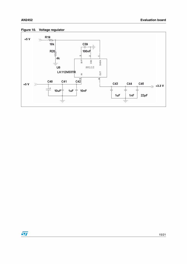
Figure 9. Low noise voltage regulator
+3.3 V low noise
+3.3 V low noise
AN2452 Evaluation board
15/21
Figure 10. Voltage regulator
+5 V
+5 V +3.3 V

Evaluation board AN2452
16/21
2.4 Layout
2.5 Bill of materials
Figure 11. Top layer Figure 12. Bottom layer
Figure 13. Ground layer Figure 14. Power layer
Table 1. Bill of materials common to all the EVBs (EVB1G/2G/4G)
Quantity Reference Part Part number - manufacturer
3 R1, R3, R4 330 Ω 0603 - PHICOMP
5 R2, R6, R7, R8, R17 2.2 kΩ 0603 - PHICOMP
1 R5 0 Ω 0603 - PHICOMP
3 R9, R10, R11 100 Ω 0603 - PHICOMP
1 R14 51 Ω 0603 - PHICOMP
1 R15 4.7 kΩ 0603 - PHICOMP

AN2452 Evaluation board
17/21
1 R16 270 Ω 0603 - PHICOMP
1 R18 8.2 kΩ 0603 - PHICOMP
1 R19 10 kΩ 0603 - PHICOMP
1 R20 4 kΩ 0603 - PHICOMP
9C8, C13, C22, C25, C33, C34,C35, C36, C40, C35, C36, C40
10 F GRM188 - 0603 - Murata
5 C1, C2, C3, C4, C38 10 pF GRM188 - 0603 - Murata
3 C6, C7, C11 15 pF GRM188 - 0603 - Murata
3 C5, C26, C39 100 nF GRM188 - 0603 - Murata
5 C10, C18, C20, C23, C45 22 pF GRM188 - 0603 - Murata
6 C9, C12, C14, C21, C24, C44 1 nF GRM188 - 0603 - Murata
1 C19 1.8 nF GRM188 - 0603 - Murata
1 C28 270 pF GRM188-COG - 0603 - Murata
1 C30 68 pF GRM188-COG - 0603 - Murata
1 C29 2.7 nF GRM188-COG - 0603 - Murata
1 C27 47 F 1210 - AVX TPS Series III
3 C31, C37, C42 10 nF GRM188 - 0603 - Murata
1 C32 100 pF GRM188 - 0603 - Murata
2 C41, C43 1 F GRM188 - 0603 - Murata
2 L3,L4 220 nH 0805HT- R22T B - Coilcraft
3 U2, U3, U4 0 Ω 0603 - PHICOMP
1 D1 LED
1 Q1 BC847C ST
1 U6 STW8110x ST
1 U7 LT1962EMS8-3.3 Linear Technology
1 U8 LK112M33TR ST
1 U9 74LCX07TTR ST
1 SMA (1.6mm) SMA REF Freq
1 SMA (1.6mm) SMA Band 2
1 J1 10 pole connector
1 J2 +5VOLT
1 J3 GND
3 S1, S2, S3 Switch
Table 1. Bill of materials common to all the EVBs (EVB1G/2G/4G) (continued)
Quantity Reference Part Part number - manufacturer

Evaluation board AN2452
18/21
Table 2. EVB1G output matching network
Quantity Reference Part Part number - manufacturer
1 Cs2 0.5 pF GRM1555C1HR50C - MURATA
1 XS1 2.1 nH 0403HQ-2N1XJL - COILCRAFT
Cs3 NC
Cs1 NC
Cs4 NC
Cs5 NC
1 C16 22 pF GRM1555C1H220J - MURATA
1 U5 0900BL15 0900BL15C050 - JOHANSON
2 C15, C17 8.2 pF GRM1555C1H8R2D - MURATA
2 R12, R13 24.9 Ω
2 L1, L2 18 nH 0403HQ-18NXJL- COILCRAFT
Table 3. EVB2G output matching network
Quantity Reference Part Part number - manufacturer
Cs2 NC
1 XS1 1.9 nH 0402PA-1N9X B - COILCRAFT
1 Cs3 1.2 pF GRM1555C1H1R2C - MURATA
Cs1 NC
Cs4 NC
Cs5 NC
1 C16 22 pF GRM1555C1H220J - MURATA
1 U5 1600BL15 1600BL15B100 - JOHANSON
2 C15, C17 22 pF GRM1555C1H220J - MURATA
2 R12, R13 51 Ω
2 L1, L2 5.5 nH 0403HQ-5N5XJL - COILCRAFT

AN2452 Evaluation board
19/21
Table 4. EVB4G output matching network
Quantity Reference Part Part number - manufacturer
1 Cs2 1.2 pF GRM1555C1H1R2C - MURATA
1 XS1 4.7 pF GRM1555C1H4R7C - MURATA
1 Cs3 1.2 pF GRM1555C1H1R2C - MURATA
Cs1 NC
1 Cs4 1 pF GRM1555C1H1R0C - MURATA
1 Cs5 1 pF GRM1555C1H1R0C - MURATA
1 C16 12 pF GRM1555C1H120J - MURATA
1 U5 3700BL15 3700BL15B100 - JOHANSON
2 C15, C17 12 pF GRM1555C1H120J - MURATA
2 R12, R13 51 Ω
1 L1, L2 5.5 nH 0403HQ-5N5XJL - COILCRAFT

Revision history AN2452
20/21
3 Revision history
Table 5. Document revision history
Date Revision Changes
17-Jul-2007 1 Initial release.
13-Aug-2007 2 Updated item 6 in Section 2.2.1: Top view.
15-Feb-2008 3Modified Section 1.2: Main form and Section 1.3: Tutorial operation mode form.Added Section 1.4: Waveform viewer.

AN2452
21/21
Please Read Carefully:
Information in this document is provided solely in connection with ST products. STMicroelectronics NV and its subsidiaries (“ST”) reserve theright to make changes, corrections, modifications or improvements, to this document, and the products and services described herein at anytime, without notice.
All ST products are sold pursuant to ST’s terms and conditions of sale.
Purchasers are solely responsible for the choice, selection and use of the ST products and services described herein, and ST assumes noliability whatsoever relating to the choice, selection or use of the ST products and services described herein.
No license, express or implied, by estoppel or otherwise, to any intellectual property rights is granted under this document. If any part of thisdocument refers to any third party products or services it shall not be deemed a license grant by ST for the use of such third party productsor services, or any intellectual property contained therein or considered as a warranty covering the use in any manner whatsoever of suchthird party products or services or any intellectual property contained therein.
UNLESS OTHERWISE SET FORTH IN ST’S TERMS AND CONDITIONS OF SALE ST DISCLAIMS ANY EXPRESS OR IMPLIEDWARRANTY WITH RESPECT TO THE USE AND/OR SALE OF ST PRODUCTS INCLUDING WITHOUT LIMITATION IMPLIEDWARRANTIES OF MERCHANTABILITY, FITNESS FOR A PARTICULAR PURPOSE (AND THEIR EQUIVALENTS UNDER THE LAWSOF ANY JURISDICTION), OR INFRINGEMENT OF ANY PATENT, COPYRIGHT OR OTHER INTELLECTUAL PROPERTY RIGHT.
UNLESS EXPRESSLY APPROVED IN WRITING BY AN AUTHORIZED ST REPRESENTATIVE, ST PRODUCTS ARE NOTRECOMMENDED, AUTHORIZED OR WARRANTED FOR USE IN MILITARY, AIR CRAFT, SPACE, LIFE SAVING, OR LIFE SUSTAININGAPPLICATIONS, NOR IN PRODUCTS OR SYSTEMS WHERE FAILURE OR MALFUNCTION MAY RESULT IN PERSONAL INJURY,DEATH, OR SEVERE PROPERTY OR ENVIRONMENTAL DAMAGE. ST PRODUCTS WHICH ARE NOT SPECIFIED AS "AUTOMOTIVEGRADE" MAY ONLY BE USED IN AUTOMOTIVE APPLICATIONS AT USER’S OWN RISK.
Resale of ST products with provisions different from the statements and/or technical features set forth in this document shall immediately voidany warranty granted by ST for the ST product or service described herein and shall not create or extend in any manner whatsoever, anyliability of ST.
ST and the ST logo are trademarks or registered trademarks of ST in various countries.
Information in this document supersedes and replaces all information previously supplied.
The ST logo is a registered trademark of STMicroelectronics. All other names are the property of their respective owners.
© 2008 STMicroelectronics - All rights reserved
STMicroelectronics group of companies
Australia - Belgium - Brazil - Canada - China - Czech Republic - Finland - France - Germany - Hong Kong - India - Israel - Italy - Japan - Malaysia - Malta - Morocco - Singapore - Spain - Sweden - Switzerland - United Kingdom - United States of America
www.st.com