Embed Size (px)
Citation preview

Studying micro-objects with Studying micro-objects with SEM (Scanning electron SEM (Scanning electron
microscope)microscope)
Student:Student:Michał Łępicki (Warsaw University of TechnologyMichał Łępicki (Warsaw University of Technology))
SupervisorSupervisor::Oleg Leonidovich OrelovichOleg Leonidovich Orelovich
Center of Applied Physics of Flerov Laboratory of Nuclear Center of Applied Physics of Flerov Laboratory of Nuclear ReactionsReactions JINR JINR

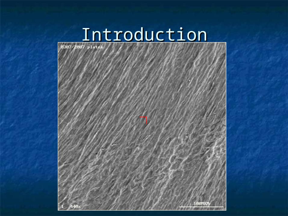
IntroductionIntroduction

IntroductionIntroduction

IntroductionIntroduction

IntroductionIntroduction
IntroductionIntroduction

IntroductionIntroduction

IntroductionIntroduction

IntroductionIntroduction

IntroductionIntroduction

IntroductionIntroduction

IntroductionIntroduction

Program of practicesProgram of practices
Layout and performance of SEMLayout and performance of SEM Preparing and coating samplesPreparing and coating samples Operating SEMOperating SEM Electron data processingElectron data processing

Layout and performance of Layout and performance of SEMSEM
1-3 Electron gun
4, 10 Aperture
5-6 Condenser lenses
7 Scanning coils
8 Stigmator
9 Objective lens
11 X-ray detector
12 Pre-amplifier
13 Scanning circuits
14 Specimen
15 Secondary electron detector
16-18 Display/Control circuits

Layout and performance of Layout and performance of SEMSEM

Preparing and coating Preparing and coating samplessamples
General view of ion sputter

Preparing and coating Preparing and coating samplessamples

Reasons of coating Reasons of coating specimensspecimens
The surface of sample must be The surface of sample must be electro conductive to minimalize electro conductive to minimalize charging from beamcharging from beam
The surface must be thermo The surface must be thermo conductive to minimalize local conductive to minimalize local heatingheating
The material of sample must have a The material of sample must have a high atomic number to increase high atomic number to increase secondary electron emissionsecondary electron emission

Preparing and coating Preparing and coating samplessamples

Preparing and coating Preparing and coating samplessamples
Gold coated sample
Sample without coating
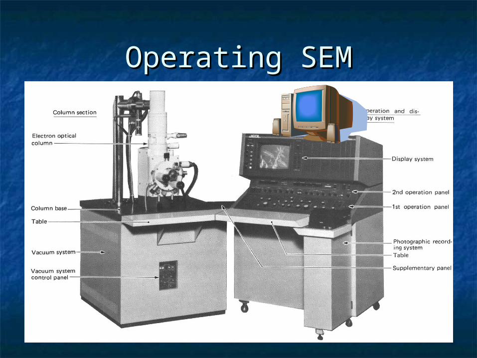
Operating SEMOperating SEM

Preparing and coating Preparing and coating samplessamples
Tilt 0 deg – shadowless illumination Tilt 30 deg

Operating SEMOperating SEM
Tilt 0 degTilt 30 deg
TIL
T
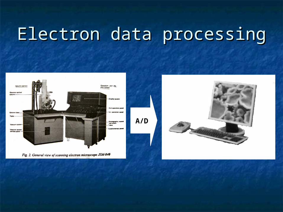
Electron data processingElectron data processing
A/D
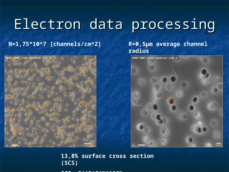
Electron data processingElectron data processingN=1,75*10^7 [channels/cm^2] R=0,5μm average channel
radius
13,8% surface cross section (SCS)
SCS= Pi*R^2*N*100%

Drain waterDrain water 70ml 70ml filtratedfiltrated

Drain waterDrain water 70ml 70ml filtratedfiltrated

Puddle water Puddle water 5050ml filtratedml filtrated

PuddlePuddle water water 50ml 50ml filtratedfiltrated

Me operating SEMMe operating SEM