Embed Size (px)
DESCRIPTION
memory
Citation preview

Study Unit
UnderstandingMemoryReviewed By
Brandon Nolta
All terms mentioned in this text that are known to be trademarks or service markshave been appropriately capitalized. Use of a term in this text should not beregarded as affecting the validity of any trademark or service mark.
About the Reviewer
Brandon Nolta has more than a decade of experience in informationtechnology, system administration, software testing, technical documentation, and freelance writing. He has worked for several companies in various technical capacities, including Hewlett-Packardand MPC. His freelance experience includes working as an Internetresearcher for the Sci-Fi Channel (now SyFy).
Mr. Nolta has a bachelor’s degree in mathematics from the Universityof Idaho and a master’s degree in English from Boise State University.He holds several technology-related certifications, including A+,Network+, and Microsoft Certified System Administrator (MCSA).
Copyright © 2011 by Penn Foster, Inc.
All rights reserved. No part of the material protected by this copyright may bereproduced or utilized in any form or by any means, electronic or mechanical,including photocopying, recording, or by any information storage and retrieval sys-tem, without permission in writing from the copyright owner.
Requests for permission to make copies of any part of the work should be mailed to Copyright Permissions, Penn Foster, 925 Oak Street, Scranton,Pennsylvania 18515.
Printed in the United States of America
01/10/12
iii
Preview
Preview
Memory can be one of the most confusing parts of a computer.There are physical differences in memory chips and many waysmemory can be accessed. This study unit contains essentialinformation about memory that, once mastered, can help youavoid much confusion.
To become a good technician, you must become familiar withmemory upgrades, access methods, SIMMs, DIMMs, DRAM,SRAM, EDO, base memory, extended memory, and XMS—allterms and acronyms related to memory. You must understandthese terms and how they’re related to the use and repair ofcomputer systems. In fact, to pass the A+ exam, you must beable to identify different categories of random access memory(RAM), their locations, and physical characteristics. In thisstudy unit, you’ll learn about the physical components ofmemory and how memory is accessed.
When you complete this study unit, you’ll be ableto
• Describe physical memory (RAM and ROM)
• Discuss the different types of ROM
• Explain the difference between RAM and storage
• Describe the different categories of RAM
• Plan memory and explore its costs
• Identify physical characteristics of SIMMs and DIMMS
• Explain different types of memory
• List different areas of memory
• Describe different ways memory can be used
• Explain how to solve memory problems
• Identify the type of memory installed on a personal com-puter (PC)
• Identify the type of memory a system board requires
• Properly install system RAM
• Upgrade cache memory
Remember to regularly check “My Courses” on your student home-page. Your instructor may post additional resources that you canaccess to enhance your learning experience.
v
TYPES OF MEMORY 1
Read-Only Memory (ROM) 2Random Access Memory (RAM) 6Parity/ECC 20
MEMORY CONFIGURATIONS 24
Chip Markings 24Form Factors 25
SELF-CHECK ANSWERS 31
Contents
Contents
1
TYPES OF MEMORY
In this study unit, you’ll learn about physical and logicalmemory. Physical memory comes in two types, randomaccess memory (RAM) and read-only memory (ROM). Typically,the term “memory” refers to RAM, or a temporary workspacefor data used by hardware devices, applications, and theCPU. “Random access” means that the CPU can access anyaddress in memory in the same amount of time as any other.
Keep in mind, though, that there’s a difference between memoryand storage. Memory values, for the most part, are temporary,being maintained and changed by electronic means. “Storage”refers to permanent storage such as on a hard drive or remov-able storage. Storage devices usually use magnetism to storevalues. When, for example, an accounting program is started,or loaded, the main pieces of the program and data locationsare transferred into memory. As the CPU requires more of theprogram or associated data, this information is swapped inand out of memory.
Anytime the CPU needs to perform a task, it quickly accessesthe addresses of the data it requires from memory, not the hard drive. A CPU may access its memory 50,000 times faster,or more, than it does its hard drive. To illustrate further:computers operate in nanoseconds, which are billionths of asecond. If it takes your CPU one second to read memory, ittakes about 14 hours to read the hard drive. Now let’s look atmemory chip types, their packages (that is, how they plug intothe computer), their capacities, and their overall advantages.
Understanding Memory
Read-Only Memory (ROM)
ROM is an integrated circuit that’s programmed with specificmicrocode. Considered a nonvolatile, or permanent, type ofmemory, ROM retains its contents when power to the computeris turned off. The IC chip programmed with its microcode isreferred to as firmware because the chip contents are “firm,” orrarely changed, and one needs special software or devices toupdate them. (Conversely, the contents of RAM are referred toas software, because they change easily and often.) AlthoughROM by general definition is “read only,” that is, programmedonly once, reprogrammable types do exist. You’ll learn aboutthese shortly.
ROM is used on system boards, video cards, modems, andother components to store data, instructions, and programsthat must be retained when power is removed from the per-sonal computer. For example, the basic input/output system(or BIOS) used to boot your computer is stored in ROM.
BIOS, which is stored within CMOS (a type of microchip funda-mental to most CPUs), contains instructions for executing the power-on self-test (POST) instructions, loading drivers forinstalled devices or utilities for keyboard and monitor, activat-ing other ROM (such as video graphics cards), and passingsystem control to the operating system. Once the OS is run-ning, BIOS provides OS and application access to the installeddevices.
Sometimes BIOS needs to be updated to accommodate a newdevice or one with larger capacity. Hard drives have increasedin storage capacity, but access to the total drive space has beenlimited by the BIOS. There have been barriers at 528 megabytes(MB), 2.1 gigabyte (GB), 8.4 GB, and 137 GB. One solution tothis problem is to use software or utilities to translate absolutehard drive addresses into logical locations. A second method isadding an adapter card with newer BIOS and capacity. Thethird solution is upgrading the present BIOS to be able to recognize and read more sectors on the hard drive, either by
Understanding Memory2

Understanding Memory 3
replacing the ROM chip itself or reprogramming it. Sometimesthis isn’t possible because of older ROM or limitations of thechipset, in which case the whole system board needs replacing.
Now we’ll look at the different characteristics of five basictypes of ROM:
• ROM
• PROM (programmable read-only memory)
• EPROM (erasable programmable read-only memory)
• EEPROM (electrically erasable programmable read-onlymemory)
• Flash memory
Because ROM chips are read-only, the microcode program-ming must be totally correct and totally complete. You typically can’t add bits of new code or make corrections toexisting code after the ROM has been burned. Creating aworkable ROM chip template is a difficult process, oftenbased on trial and error. ROM, by definition, isn’t changeableonce it’s programmed. If data is incorrect or new devicesneed to be added or updated, the ROM needs to be replacedon the system board.
But the advantages of ROM outweigh the difficulties. Once thetemplate is tested and complete, the cost to duplicate the ROMis relatively inexpensive. ROMs are reliable, have low powerrequirements, and generally contain all the code necessary torun associated devices.
Now we’ll look at each of these types of ROM in detail.
ROM
As we’ve mentioned, the information held in ROM isn’t lostwhen power is turned off. This type of memory is called non-volatile memory. The manufacturer programs the ROM byburning it into the chip. The way a ROM chip works requiresthe programming of correct and complete data when the chip iscreated. Though it can be tricky to create an original ROM tem-plate, the process is usually worth it. With a finished template,
the chips themselves are usually very inexpensive. They don’tuse a lot of power, usually contain all the programming neces-sary to control a device, and can be depended on to performconsistently. Of course, you can’t reprogram or rewrite astandard ROM chip. If it contains bad data or needs to beupdated, you have to scrap the chip and create a new one.
Programmable ROM (PROM)
ROM programming limitations, the expense of creating original templates, and the cost of generating small ROMbatches led to the development of reprogrammable ROM. The first type is programmable read-only memory, or PROM.PROM chips are inexpensive and formatted with a devicecalled a programmer.
Like regular ROM, PROM memory addresses are arranged in rows and columns. However, a fuse is located at eachaddress. An address where the fuse is melted is classified as0 (signifying “off”), and an address where the fuse is whole,or unmelted, is classified as a 1 (signifying “on”). Prior to programming, all fuses are whole and all addresses are setas 1s. The PROM programmer tool can selectively melt fuseaddresses, setting up patterns of 1s and 0s that translateinto program microcode.
Because PROM consists of an array of fuses, it’s more fragilethan regular ROM and thus susceptible to corruption by staticelectricity (blown fuse). Also, to program PROM, it must beremoved from the system board. Care must be taken not todamage PROM pins or stretch the holes on the system board.Inexpensive and programmable as it is, PROM is sometimesused in the trial-and-error generation of the permanent ROMtemplate. Early disadvantages of limited reuse and chip-handling problems pushed developers toward a better, moreversatile PROM.
Understanding Memory4
Understanding Memory 5
Erasable Programmable ROM (EPROM)
EPROM is similar to PROM, except that it can be erased and reused. Software occasionally needs to change, so itbecame important to be able to update the ROM. To updateROM in older computers, you needed to replace the chips.Newer systems are upgraded by simply running a program.EPROMs have a small window on the top of the chip that canbe uncovered and exposed to a specific frequency of high-inten-sity ultraviolet light. Exposure of about 15 minutes erases theEPROM (chemically melting the fuses back together and settingthem all to 1s) and allows it to be rewritten with new data. TheEPROM must be completely erased before you can write newcode to the chip. Of course, special equipment is needed forthese operations. Nevertheless, EPROM is cheaper to make andburn than PROM. If a mistake is made, EPROM chips can beerased and reused. Though EPROMs are a major improvementover PROMs, they still require dedicated equipment and a labor-intensive process to remove and reinstall them each time achange is needed. In addition, changes can’t be made incremen-tally to an EPROM; the entire chip must be erased.
Electronically Erasable Programmable ROM(EEPROM)
Two of the drawbacks to EPROMs are (1) you still need dedi-cated equipment to modify the code on the chip, and (2) the chip must be physically removed from the system board.The chip is mounted in through-hole sockets on the systemboard. Repeatedly removing the chip contributes to chipcreep, in which the chip gradually begins to work its way out. This can cause parity errors or ROM reliability problems.However, the development of EEPROM has bypassed thesesetbacks. Instead of using ultraviolet light, EEPROM appliesa higher electrical charge, erasing selective bytes and allow-ing new data to be written. This is done with software “on

the fly,” meaning that you don’t have to remove the chip from the system board, and the computer system is runningas the chip is being flashed.
BIOS chips are now typically EEPROMS. While versatile,EEPROMS are modified only one byte at a time, a rate thatcan be too slow for devices requiring rapid and repeated codeupdates. Flash memory was the next evolutionary step thathelped solve this speed limitation.
Flash Memory
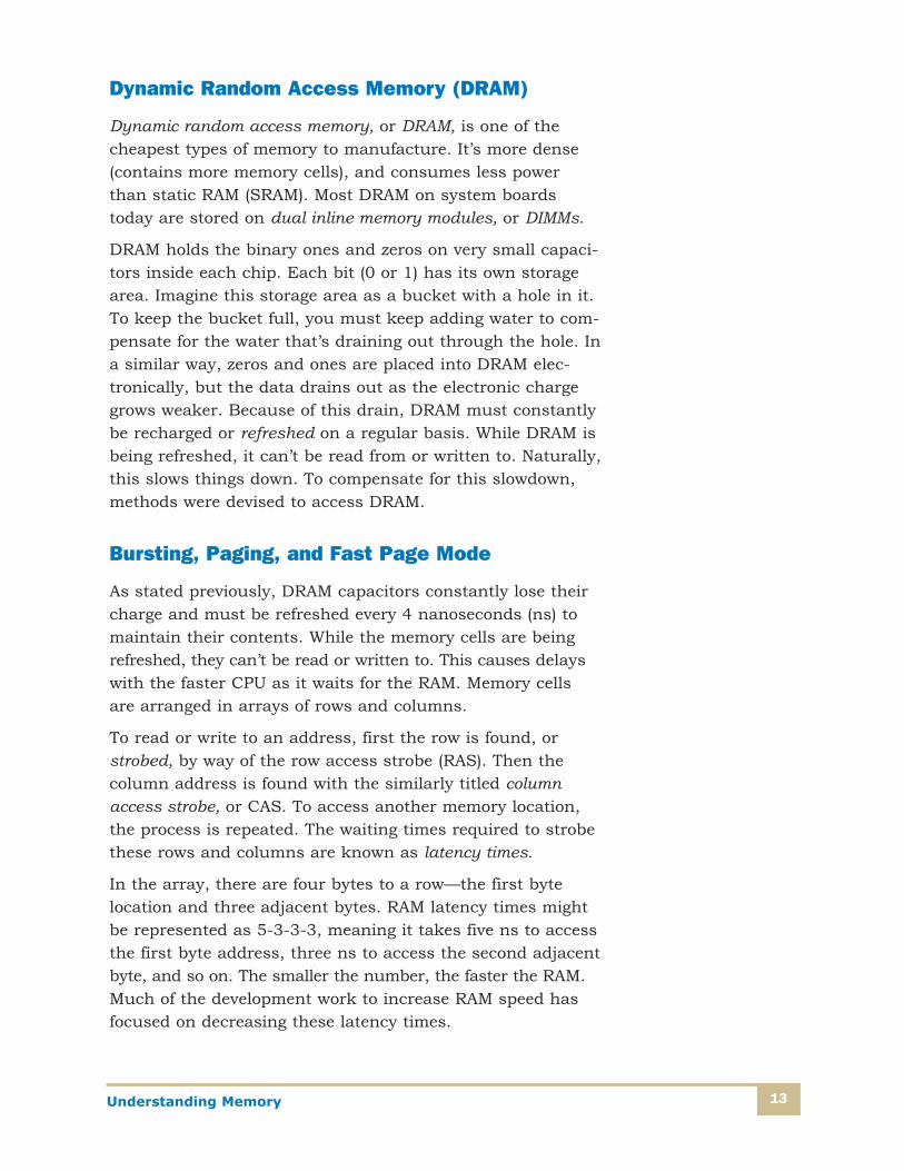
Flash memory is many times faster than EEPROM, because it can access a block of addresses—the entire chip—insteadof a single byte. System board BIOS chips made since 1994are EEPROMS or flash EEPROMS. Flash memory is also pack-aged as removable external PCMCIA cards for laptops, digitalcameras, and game consoles (Figure 1). Because of theirmemory capacities (from 2 GB to 286 GB; their nonvolatility,or ability to maintain data for decades; and their easy trans-portability, flash memory cards are more like storage thanmemory. But unlike storage devices with moving parts, flashis solid-state, or totally electronic, and this adds to its durabilityand speed.
Understanding Memory6
FIGURE 1—Flash MemoryCards
Understanding Memory 7
Random Access Memory (RAM)
The random access memory, or RAM, of a computer can becompared to the surface of your desk. When you’re working,you have papers and books spread out and you can refer toeach of them. The larger your desk, the more things you canspread out on it. In addition, while you’re working, you don’thave to start at one corner of the desk and check each itemuntil you come to the book you want. Instead, you can godirectly to that book wherever it’s located on the desktop.When you’re finished with a book, you can put it away andfree up space on the desk. When you need another book foryour work, you can place it on the desktop for easy referenceas long as there’s space left for it. When you’re done with theproject, you remove all of the books and papers from thedesk and store them on shelves or in files.
In a computer system, running applications store informa-tion about themselves, addresses, requested services, anddata locations in RAM. The central processing unit (CPU) canaccess a particular memory location in RAM and retrieve thedata that’s stored in that location. The amount of RAM canbe compared to the size of the desktop. Like the desktop,RAM has a set amount of space that can be filled with data.The data stored in RAM is there only temporarily. When thecomputer is turned off, the contents of RAM are erased,which is a lot like clearing off the desk. If you haven’t savedthe data, it will be lost when the computer loses power. Thiswould be similar to being in the middle of a project and hav-ing someone come into your office and permanently removeall of the papers and books from the desktop even thoughyou still might need them. Because the contents of RAM areerased when you turn off the computer, RAM is considered to be volatile memory, that is, the data will disappear when power is turned off. Hard-drive storage is considered nonvolatile memory. Data saved to the hard drive remainsthere until it’s purposely deleted.
Understanding Memory8
What’s the Difference between System Memoryand Storage Capacity?
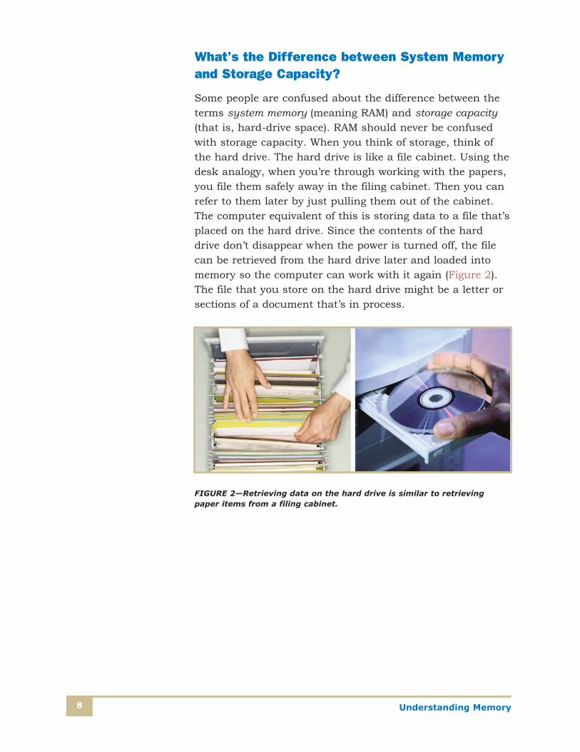
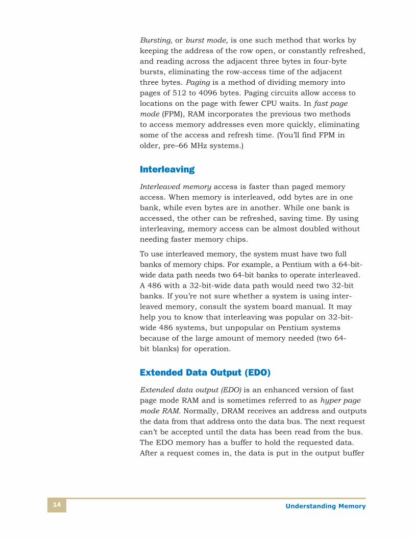
Some people are confused about the difference between theterms system memory (meaning RAM) and storage capacity(that is, hard-drive space). RAM should never be confusedwith storage capacity. When you think of storage, think ofthe hard drive. The hard drive is like a file cabinet. Using thedesk analogy, when you’re through working with the papers,you file them safely away in the filing cabinet. Then you canrefer to them later by just pulling them out of the cabinet.The computer equivalent of this is storing data to a file that’splaced on the hard drive. Since the contents of the harddrive don’t disappear when the power is turned off, the filecan be retrieved from the hard drive later and loaded intomemory so the computer can work with it again (Figure 2).The file that you store on the hard drive might be a letter orsections of a document that’s in process.
FIGURE 2—Retrieving data on the hard drive is similar to retrievingpaper items from a filing cabinet.
Understanding Memory 9
System memory is generally measured in units called mega-bytes (MB) or gigabytes (GB). A typical system might come with2 GB, or 2,000,000,000 bytes of RAM. Hard-drive capacity, onthe other hand, is much larger and is usually measured in ter-abytes (TB) rather than in megabytes or gigabytes.
Remember that prefixes before the word byte denote multipleamounts of bytes. Also, remember that there are eight binarydigits, or bits, per byte. A kilobyte (abbreviated K or KB) equalsone thousand bytes, a megabyte (meg or MB) equals one millionbytes, a gigabyte (gig or GB) equals one billion bytes and a terabyte (TB) equals one trillion bytes or a thousand gigabytes.The motherboard chipset, the memory controller, and the widthof the address bus will limit the amount of RAM accessible by the system. There are methods for getting around these
limitations—upgrading ROM, utilizing special software, or logical addressing, but upper limits still exist. The 32-bit desk-top versions of Microsoft Windows operating systems (2000Professional, XP, NT 4.0) are limited to four gigabytes of physi-cal RAM. Using Intel’s Pentium IV processor and 36-bit pageextended addressing (PAE-36), Advanced Server and DatacenterServer editions take an extra four bits for addressing and sup-port up to 64 gigabytes of RAM. Current versions of MicrosoftWindows operating systems (Windows Vista, Windows 7) are64-bit, and can physically address up to 2 TB of physicalRAM; however, limitations in the software restrict theamount of usable RAM to 192 GB for the Ultimate,Professional and Enterprise versions.For more detailed infor-mation, go to the Intel Web site at http://www.intel.com.
Professional TipIf you hear someone say, “My computer has 80 gigabytes of memory,” you should immediately suspect that the person is confusing memory with storage capacity. Most likely, the person’ssystem has an 80 GB hard drive, since most desktop computerswouldn't have 80 GB of RAM.
How Computers Communicate
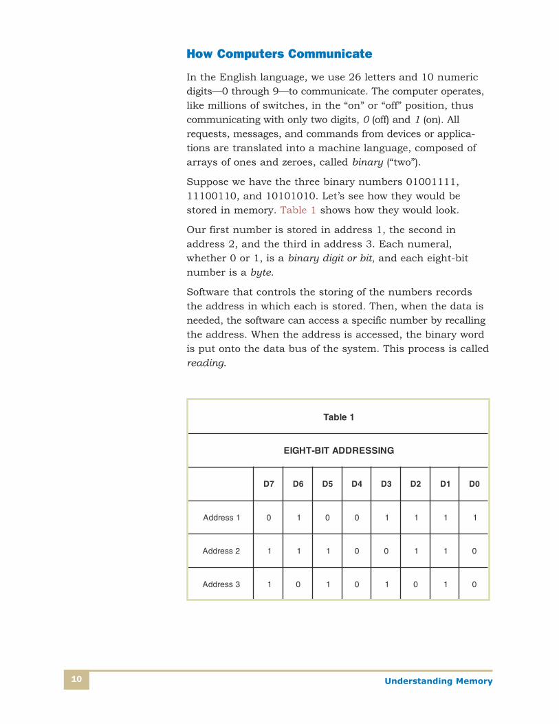
In the English language, we use 26 letters and 10 numericdigits—0 through 9—to communicate. The computer operates,like millions of switches, in the “on” or “off” position, thuscommunicating with only two digits, 0 (off) and 1 (on). Allrequests, messages, and commands from devices or applica-tions are translated into a machine language, composed ofarrays of ones and zeroes, called binary (“two”).
Suppose we have the three binary numbers 01001111,11100110, and 10101010. Let’s see how they would bestored in memory. Table 1 shows how they would look.
Our first number is stored in address 1, the second inaddress 2, and the third in address 3. Each numeral,whether 0 or 1, is a binary digit or bit, and each eight-bitnumber is a byte.
Software that controls the storing of the numbers records the address in which each is stored. Then, when the data isneeded, the software can access a specific number by recallingthe address. When the address is accessed, the binary wordis put onto the data bus of the system. This process is calledreading.
Understanding Memory10
1elbaT
GNISSERDDATIB-THGIE
7D 6D 5D 4D 3D 2D 1D 0D
1sserddA 0 1 0 0 1 1 1 1
2sserddA 1 1 1 0 0 1 1 0
3sserddA 1 0 1 0 1 0 1 0

Understanding Memory 11
Let’s assume that you’re working with word processing softwareand preparing a document. Each letter has a binary equivalentthat’s stored in a memory address. Then you discover you’vemade a typing error, so you go back to the letter that’s incorrectand put in the correct letter. Now the new letter would haveto be stored to the memory address previously occupied bythe old letter. The binary equivalent of the new letter wouldbe put on the data bus and moved to the memory address.This process is called writing.
In an ideal situation, the reading and writing of data wouldhappen instantly, but in reality, that’s not the way thingswork. It takes time to access memory. How much time? Thatvaries, which explains why memory is rated with an accesstime. Access time is the time it takes to read from or write toa memory location. It’s the delay from the time the memorychip is given an address to the time when the data is avail-able at the data lines. This time is measured in nanoseconds(ns). One nanosecond equals one billionth of a second (thatis, 0.000000001 second). That doesn’t sound like very muchtime in human terms, but in a fast computer system, a few nanoseconds can mean a big performance increase ordecrease. Memory chips have their access time marked onthem. For example, a notation of “70” on a chip refers to a 70 ns access time. A notation of “60” indicates a 60 nsaccess time. The smaller the number, the less access timeand the faster the chip. Most current RAM has access timesin the 3.4–5 ms range.
You’re probably wondering if you could increase the computer’sspeed by simply replacing slower chips with faster chips.That’s a good thought, but it won’t work. The system boarddesign and CPU determine the speed at which the computercan function. When the 80286 processor came out, systemdesigners found that the memory that was in use for comput-ers based on the 8086/8088 processor-based computerswasn’t fast enough for the 286 CPU. The 286 could read fromand write to memory locations faster than the memory couldoperate. This situation meant that the CPU would try to out-put data to memory so fast that it would be sending newdata before the last data had been written into a memoryaddress. You can see how that would lead to errors. Attemptsto read from memory also caused problems since requests
would be sent faster than data could be made available frommemory. To remedy the situation, wait states were designedinto the system board. A wait state is a time delay before theCPU accesses the memory. This means that the CPU wouldoutput data, and then wait for a specified time so the CPUcould safely write the data to memory before more data wouldbe output. In the case of reading from memory, the CPUwould request data from a specific address, then wait for thepredetermined time before making another request. The timedelay compensated for the slower memory access times.
Adding wait states slows down the system. However, that’sthe whole idea. It doesn’t make sense to have a fast systemthat makes many errors and loses data. The addition of waitstates allows the system to operate reliably. It can accuratelyread from or write to memory. Older systems used wait statesto solve the problem of a CPU that could operate faster thanthe memory could function. The disadvantage of the wait statesolution was that a faster CPU didn’t really give a system muchof an advantage. Newer systems use a different approach,involving a cache, to better use faster CPUs.
Types of RAM
Let’s review a few things that you should understand by nowabout RAM. RAM is the term that’s used to describe the com-puter’s working memory. RAM has two distinct characteristics.First, RAM is volatile. This means that if the chip doesn’thave power applied to it, all information stored in the chipwill be lost. RAM is ideal for loading and running programsand data needed for the computer to operate. Second, RAMcan be written to and read from, so the information stored at any particular address is subject to change.
Some storage media are sequential, such as magnetic tape.To go to a location on the tape, you much first go through allprevious locations. The term random access memory refers tothe fact that all locations in memory can be accessed equallyand in the same amount of time. This term applies to all thedifferent types of RAM.
Understanding Memory12
Understanding Memory 13
Dynamic Random Access Memory (DRAM)
Dynamic random access memory, or DRAM, is one of thecheapest types of memory to manufacture. It’s more dense(contains more memory cells), and consumes less power than static RAM (SRAM). Most DRAM on system boards today are stored on dual inline memory modules, or DIMMs.
DRAM holds the binary ones and zeros on very small capaci-tors inside each chip. Each bit (0 or 1) has its own storagearea. Imagine this storage area as a bucket with a hole in it.To keep the bucket full, you must keep adding water to com-pensate for the water that’s draining out through the hole. Ina similar way, zeros and ones are placed into DRAM elec-tronically, but the data drains out as the electronic chargegrows weaker. Because of this drain, DRAM must constantlybe recharged or refreshed on a regular basis. While DRAM isbeing refreshed, it can’t be read from or written to. Naturally,this slows things down. To compensate for this slowdown,methods were devised to access DRAM.
Bursting, Paging, and Fast Page Mode
As stated previously, DRAM capacitors constantly lose theircharge and must be refreshed every 4 nanoseconds (ns) tomaintain their contents. While the memory cells are beingrefreshed, they can’t be read or written to. This causes delayswith the faster CPU as it waits for the RAM. Memory cellsare arranged in arrays of rows and columns.
To read or write to an address, first the row is found, orstrobed, by way of the row access strobe (RAS). Then the column address is found with the similarly titled columnaccess strobe, or CAS. To access another memory location,the process is repeated. The waiting times required to strobethese rows and columns are known as latency times.
In the array, there are four bytes to a row—the first bytelocation and three adjacent bytes. RAM latency times mightbe represented as 5-3-3-3, meaning it takes five ns to accessthe first byte address, three ns to access the second adjacentbyte, and so on. The smaller the number, the faster the RAM.Much of the development work to increase RAM speed hasfocused on decreasing these latency times.
Understanding Memory14
Bursting, or burst mode, is one such method that works bykeeping the address of the row open, or constantly refreshed,and reading across the adjacent three bytes in four-bytebursts, eliminating the row-access time of the adjacent three bytes. Paging is a method of dividing memory intopages of 512 to 4096 bytes. Paging circuits allow access tolocations on the page with fewer CPU waits. In fast pagemode (FPM), RAM incorporates the previous two methods to access memory addresses even more quickly, eliminatingsome of the access and refresh time. (You’ll find FPM inolder, pre–66 MHz systems.)
Interleaving
Interleaved memory access is faster than paged memoryaccess. When memory is interleaved, odd bytes are in onebank, while even bytes are in another. While one bank isaccessed, the other can be refreshed, saving time. By usinginterleaving, memory access can be almost doubled withoutneeding faster memory chips.
To use interleaved memory, the system must have two fullbanks of memory chips. For example, a Pentium with a 64-bit-wide data path needs two 64-bit banks to operate interleaved.A 486 with a 32-bit-wide data path would need two 32-bitbanks. If you’re not sure whether a system is using inter-leaved memory, consult the system board manual. It mayhelp you to know that interleaving was popular on 32-bit-wide 486 systems, but unpopular on Pentium systemsbecause of the large amount of memory needed (two 64-bit blanks) for operation.
Extended Data Output (EDO)
Extended data output (EDO) is an enhanced version of fastpage mode RAM and is sometimes referred to as hyper pagemode RAM. Normally, DRAM receives an address and outputsthe data from that address onto the data bus. The next requestcan’t be accepted until the data has been read from the bus.The EDO memory has a buffer to hold the requested data.After a request comes in, the data is put in the output buffer
Understanding Memory 15
while the next request is read. Thus, EDO RAM can operatemuch faster than regular DRAM. EDO RAM works well withsystems that have bus speeds up to 66 MHz (that is, PCsthat were manufactured prior to 1998). However, the marketfor EDO RAM declined due to the emergence of SDRAM,which we’ll discuss in the next section.
EDO also uses burst mode to decrease access times. Thisreduces overall cycle time by five percent, which is a signifi-cant amount when dealing with MHz speeds. EDO uses thesame technology as FPM and costs roughly the same, butEDO is faster; this is why FPM has become obsolete. BurstEDO, or BEDO, was a short-lived enhancement with evenfaster burst-speed features. Intel developed BEDO DRAM,but only one system board chipset supported it, and theenhancement was soon replaced by synchronous DRAMtechnology.
Synchronous Dynamic Random Access Memory(SDRAM)
In normal DRAM, the CPU waits for the RAM capacitors torefresh and then access memory addresses. As explained ear-lier, because RAM speed falls short of the speed of the CPU,delays (or waits) occur that increase the overall processing time.Synchronous DRAM, or SDRAM, eliminates these waits by work-ing within the cycle time of the system clock. Because the RAMis synchronized with the clock cycle, the memory controllerknows exactly when the requested data will be available for theCPU; thus, the CPU no longer has to wait. System clock pulsesare generated by an oscillator clock on the motherboard, andthe CPU and RAM are synchronized with this clock rate viacontrollers. For machines developed before the adoption of DDRmemory, which will be explained in a later section, a typicalclock rate might be 100 megahertz (MHz), which is 100 millionclock ticks, or cycles, per second. PC100 SDRAM supports thisbus speed and, as specified by Intel, has an access time of 8ns. (Remember that a nanosecond is one billionth of a second.)
Understanding Memory16
In the above 100 MHz example, dividing one billion nanosec-onds per second by 100 million clock cycles per second yields10 ns per clock cycle. And yet, to successfully meet all timingparameters, the PC 100 RAM is actually faster than 10 ns—it’s 125 MHz, or 8 ns.
Older SDRAM that supported 66 MHz systems could becalled PC66 RAM (15 ns). PC133 RAM (7.5 ns) is supportedby a 133 MHz bus and chipset. SDRAM uses burst mode andpipelining, in which the memory controller simultaneouslyreads, sends, and writes data, to further increase speed. Inour example, the PC100 latency times would be eight clockcycles (8 ns) to read four bytes of data. This is almost twiceas fast as older FPM RAM.
Enhanced SDRAM (ESDRAM)
RAM enhancements up to this point have tried to increaseRAM speed by decreasing RAS and CAS delays. EnhancedSDRAM (from Enhanced Memory Systems) achieves this by incorporating some faster SRAM within the DRAM chip towork as row register cache. This allows faster internal func-tionality of the memory module. The SRAM also has a widebus directly connecting it to the DRAM, which increasesbandwidth. This architecture can run at 166 MHz or 6 ns (latency times 2-1-1-1). Typically, ESDRAM is used for L2cache and competes with DDR SDRAM as a replacement forSocket 7 processor SDRAM.
Double-Data-Rate Synchronous DRAM(DDR SDRAM)
Double-data-rate synchronous DRAM (DDR SDRAM), sometimes called SDRAM II, is a next-generation SDRAMtechnology. It allows the memory chip to perform transac-tions on both the rising and falling edges of the clock cycle.For example, with DDR SDRAM, a 100 or 133 MHz memorybus clock rate yields an effective data rate of 200 MHz or 266 MHz.
New naming conventions based on speed are used with DDRSDRAM. Remember that giga means “billion,” so 1 GB/srefers to a transfer rate of approximately one billion bytes,
Understanding Memory 17
or 1024 megabytes per second. DDR200 equals 1.6 GB/sand is referred to as PC1600; DDR333 equals 2.7 GB/s andis referred to as PC2700. The speed is roughly derived bymultiplying the amount in MHz by 8 bytes (a 64-bit bus cantransfer 8 bytes per cycle). Thus, DDR333 is
333 MHz (million cycles/second) � 8 bytes
or approximately 2.7 GB/second. Note that placing PC2700in a PC1600 system board will yield no more than PC1600 performance-wise.
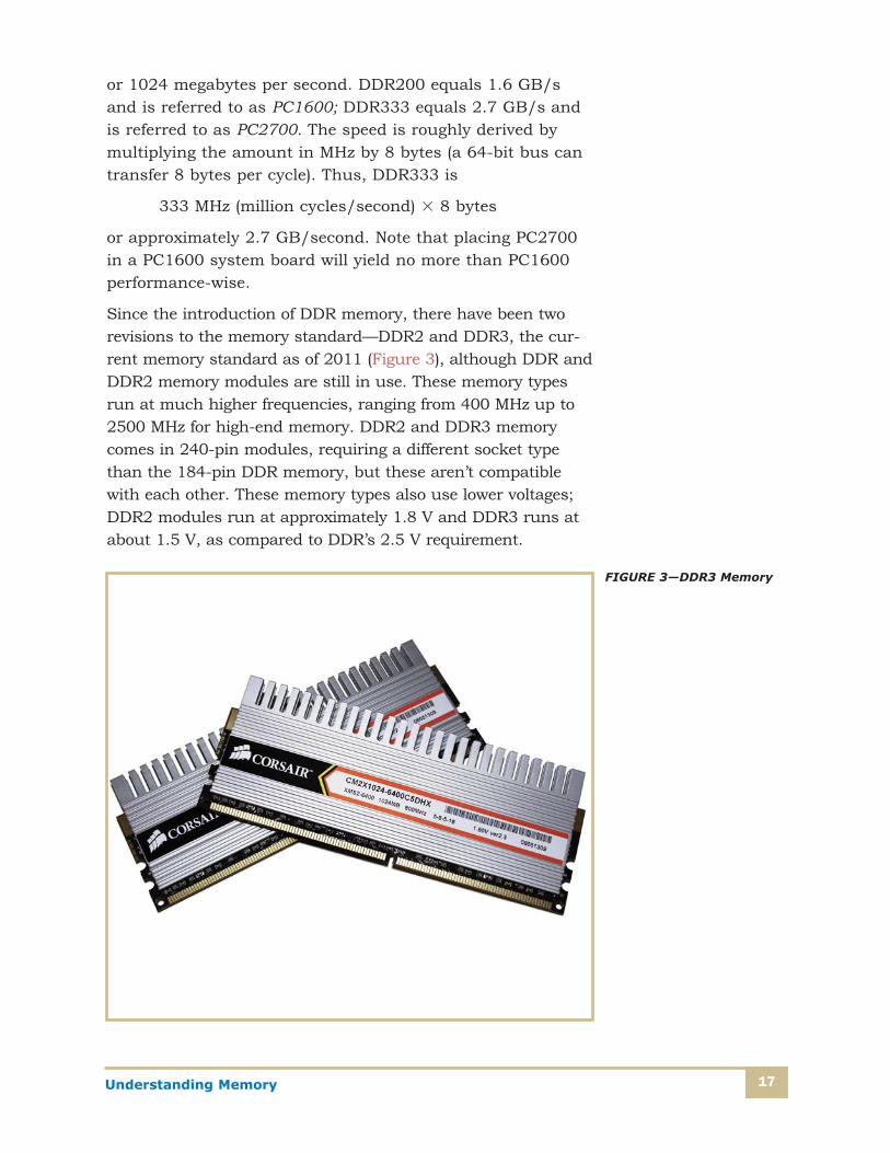
Since the introduction of DDR memory, there have been tworevisions to the memory standard—DDR2 and DDR3, the cur-rent memory standard as of 2011 (Figure 3), although DDR andDDR2 memory modules are still in use. These memory typesrun at much higher frequencies, ranging from 400 MHz up to2500 MHz for high-end memory. DDR2 and DDR3 memorycomes in 240-pin modules, requiring a different socket typethan the 184-pin DDR memory, but these aren’t compatiblewith each other. These memory types also use lower voltages;DDR2 modules run at approximately 1.8 V and DDR3 runs atabout 1.5 V, as compared to DDR’s 2.5 V requirement.
FIGURE 3—DDR3 Memory
Understanding Memory18
Static RAM (SRAM)
The term static means “fixed” or “unmoving.” Static RAM, orSRAM, doesn’t have to be refreshed to maintain its contents.SRAM is composed of six transistors at each memory cell.The memory contents are maintained as long as power isapplied to the transistors. Unlike DRAM, SRAM doesn’t havecapacitors that need refreshing; therefore, row/column latencyisn’t an issue. This drastically lowers access times and makesSRAM much faster than DRAM. Access times for SRAM canbe less than 2 ns, while typical access times for DRAM arebetween 60 and 70 ns. This is why SRAM is used in smallamounts for cache and DRAM is used as the main systemmemory. You may ask, why not use SRAM for all of the systemmemory if it’s so much faster? Unfortunately, SRAM costs moreto manufacture than DRAM, consumes more power, and has a higher density. This means that 2 MB of SRAM takes up thesame physical space as 64 MB of DRAM.
Rambus DRAM (RDRAM)
So far, approaches to increasing system memory performancehave included
1. Tweaking RAM access times—decreasing latency times,increasing data flow with interleaving, burst pipelining,and synchronization
2. Adding SRAM caches on DRAM memory modules, onCPUs, and externally on the system board
3. Increasing the width of the buses
The Rambus approach to breaking the barriers of RAMspeeds and bus speeds was designing a new architecture. At the time of introduction, the memory bus standard wasonly 16 bits wide and transferred data at a rate of two bytesper cycle. A single-channel module (168 or 184 pins) had a typical bus speed of 800 MHz, or 1.6 GB/second. Dual-channel 800 MHz RDRAM incorporated two channels on one 242-pin module and ran at 3.2 GB/second. This is comparable to the dual-channel PC3200 DDR RAM platform.However, Rambus memory had some technical deficiencies;RDRAM module, or RIMM, architecture required all memory

Understanding Memory 19
slots to be filled, necessitating a continuity RIMM (C-RIMM)be installed if there were more memory slots than modulesavailable. RIMMs were also expensive—two to three times as expensive as regular RAM—ran very hot, and had highlatency periods. Due to these technical issues, a number ofhigh-profile intellectual-property disputes with other memorymanufacturers and the development of faster memory tech-nologies, RIMMs never became popular in the computingcommunity, and are largely discontinued from use, except in certain specialized applications.
What Is Cache?
A cache is a small amount of high-speed memory, the size ofwhich varies. This high-speed memory is known as staticRAM (SRAM). Static RAM operates much faster than dynamicRAM (DRAM), which is used for the system’s main memory.When the CPU requests information, a cache controller that’sdesigned into either the CPU or system board loads chunksof the DRAM into the SRAM. The next time the CPU needsinformation, the cache is checked first; if the needed data isthere, it’s loaded into the CPU, speeding up the process. Thecache uses a “best guess” method to anticipate what the CPUwill need next. It loads chunks of the DRAM into the SRAMwhile the CPU is busy doing calculations. This operation dramatically increases the speed of the system because theaccess time of the SRAM is faster than the access time of the DRAM. The CPU doesn’t have to wait as long betweenrequests for data.
Cache can be designed into the system board, with SRAMchips installed on the system board. Alternatively, the cachecan be inside the CPU, which increases the performance ofthe system even more.
There are two main types of cache: Level (L1) and Level 2(L2). A Level 1 cache (often called an internal cache or L1cache) is built into the CPU itself. This significantly increasesthe speed of the CPU. A Level 2 cache is designed outside the CPU on the system board and is often called an externalcache or L2 cache. L2 cache also increases the system’sspeed, but not always as much as a L1 cache. Many systemshave both a Level 1 and a Level 2 cache incorporated into
Understanding Memory20
them. This combination gives an even greater performanceboost than either type of cache alone. Although not as com-mon yet, there is a third type of cache, Level 3 (L3) cache,which is the cache memory farthest from the core, but stillpart of the overall processor system. L3 cache is most preva-lent on multi-core processor systems. Cache memory will bediscussed in more detail in the next section.
Parity/ECC
Error checking and correcting (ECC) and parity memory mod-ules don’t perform any error detection or correction functionsthemselves. Error checking and correction functions are carried out on the system board, not on the memory moduleitself. The modules simply provide the space required tostore the extra bits of data that represent the condition ofthe real data. The computers always calculate parity andECC data for every read and write.
Parity
Parity is an older, low-level, single-bit error detection method.The default parity method was called odd parity and will beused as our example.
Recall that memory is an array of capacitors that act likeswitches, turned on or off. “On” is represented by the binarydigit (bit) 1, and “off” is represented by 0. For each byte (8 bits) of a memory word, one extra bit (the 9th) is used tokeep track of whether the total number of 1s, or “on” bits, isan odd or even number. If it’s odd, then the parity bit stays0, and if it’s even, the parity bit is set to 1. The number ofon bits plus the parity bit will always be an odd number. As data is written to memory, the parity generator/checkergenerates the parity bit. When the data is read from mem-ory, the checker circuit tallies the number of one bits,including the parity bit. If the number is even, the circuitknows that an error has occurred, and a parity error mes-sage is triggered. An interrupt also occurs, which halts thesystem. The system must then be restarted.
Understanding Memory 21
Because parity identifies only odd or even quantities, twoincorrect bits can go undetected. In addition, there’s no wayto tell which bit is in error, and bad bits aren’t corrected.One positive aspect of parity checking is that it doesn’t slowsystem performance, since it’s done in tandem with memoryread or write operations.
Parity has lost favor over the years for several reasons:
• Parity can’t correct errors.
• Some errors go undetected.
• Errors result in complete system shutdown, which cancause damage to data.
• DRAM has become significantly more reliable.
• Current computer operating systems don’t handle parityerrors as smoothly as older operating systems.
• For many users, the low level of protection doesn’t justifythe cost of the extra chips.
ECC
ECC, or error checking and correcting, permits error detectionas well as correction of certain errors. Typically, ECC candetect single- and dual-bit errors, and can correct single-biterrors. Error detection and correction are done “on the fly”without the operating system even being aware of it. Thememory controller chip on the system board performs thecorrection and always sends corrected data to the CPU. Thememory controller can inform the operating system whenerrors are corrected, but most have no means of logging thecorrections or informing the user. So, the user may neverknow an error ever occurred.
Multibit errors are so rare that further detection and correc-tion capabilities are required only in extreme cases, andwould require custom memory components. For that level of protection 100% redundancy would probably be lessexpensive by using single-bit correction memory modules on two separate memory subsystems. Double-bit detection/
Understanding Memory22
single-bit correction ECC functions may require more orfewer extra bits than parity depending on the data path. Forexample:
• 8-bit data path requires 5 bits for ECC or 1 bit for parity.
• 16-bit data path requires 6 bits for ECC or 2 bits for parity.
• 32-bit data path requires 7 bits for ECC or 4 bits for parity.
• 64-bit data path requires 8 bits for ECC and 8 bits forparity.
• 128-bit data path requires 9 bits for ECC or 16 bits forparity.
There’s a break-even point at 64 bits. At this point, the securityof ECC costs the same (in DRAM) as the less capable parity.The efficiency of ECC versus parity in today’s 64-bit processorsand the inevitably wider data paths of future processorsmake continued use of parity highly improbable.
Take a few moments now to test your understanding by completing Self-Check 1.

Understanding Memory 23
Self-Check 1At the end of each section of Understanding Memory, you’ll be asked to pause and check your understanding of what you have just read by completing a “Self-Check” exercise. Answering these questions will help you review what you’ve studied so far.Please complete Self-Check 1 now.
1. What part of the manufactured system board is likely flash memory?
__________________________________________________________
2. Which memory is faster, EDO or BEDO?
__________________________________________________________
3. Explain why static RAM (SRAM) is faster than DRAM.
__________________________________________________________
__________________________________________________________
4. Describe the difference between what happens when parity checking discovers an error andwhen ECC discovers an error.
__________________________________________________________
__________________________________________________________
__________________________________________________________
Check your answers with those on page 31.
Understanding Memory24
MEMORY CONFIGURATIONS
Chip Markings
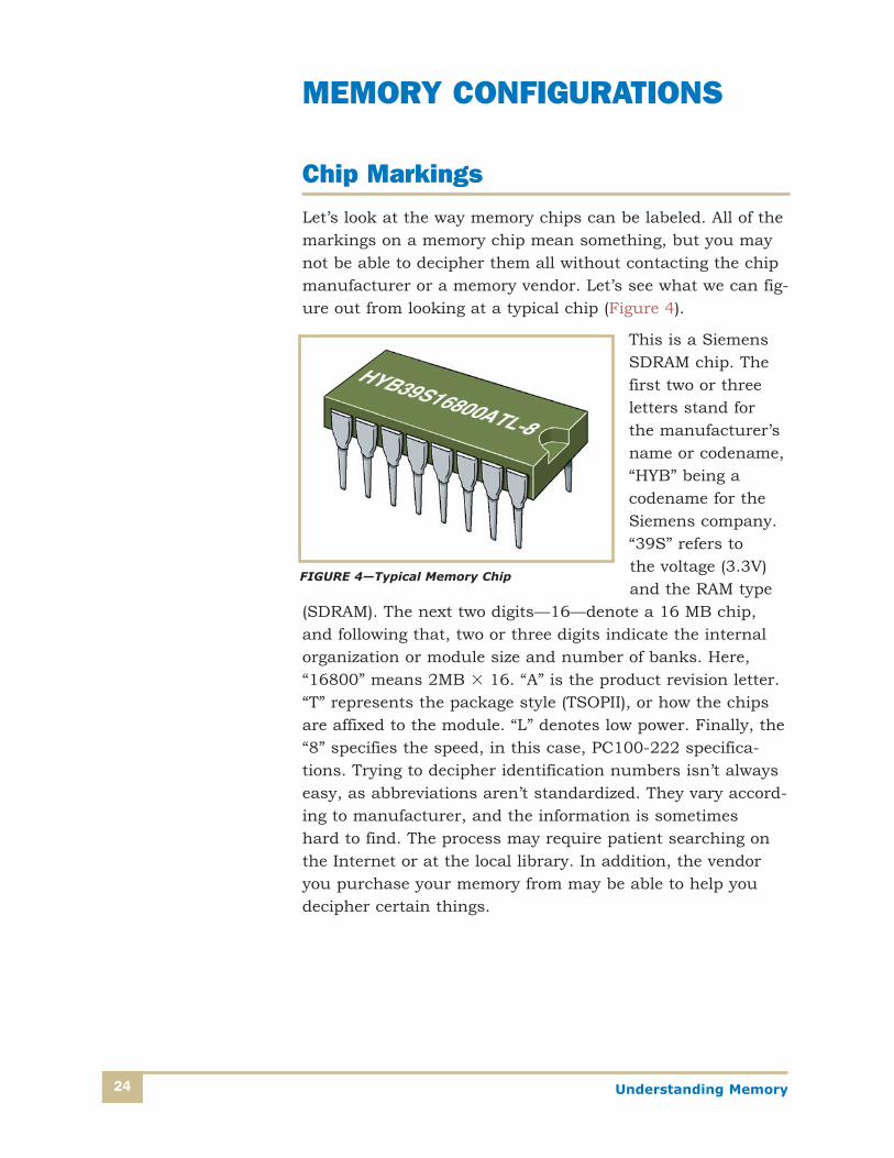
Let’s look at the way memory chips can be labeled. All of themarkings on a memory chip mean something, but you maynot be able to decipher them all without contacting the chipmanufacturer or a memory vendor. Let’s see what we can fig-ure out from looking at a typical chip (Figure 4).
This is a SiemensSDRAM chip. Thefirst two or threeletters stand for the manufacturer’sname or codename,“HYB” being a codename for theSiemens company.“39S” refers to the voltage (3.3V)and the RAM type
(SDRAM). The next two digits—16—denote a 16 MB chip,and following that, two or three digits indicate the internalorganization or module size and number of banks. Here,“16800” means 2MB � 16. “A” is the product revision letter.“T” represents the package style (TSOPII), or how the chipsare affixed to the module. “L” denotes low power. Finally, the“8” specifies the speed, in this case, PC100-222 specifica-tions. Trying to decipher identification numbers isn’t alwayseasy, as abbreviations aren’t standardized. They vary accord-ing to manufacturer, and the information is sometimes hard to find. The process may require patient searching onthe Internet or at the local library. In addition, the vendoryou purchase your memory from may be able to help youdecipher certain things.
FIGURE 4—Typical Memory Chip
Understanding Memory 25
Form Factors
Memory comes in different packages or forms. Originally,chips were single entities called single inline pin packages, orSIPPs, each of which contained one row of pins and were sol-dered to the system board. Then came dual inline packages,or DIPs, which housed a row of pins on either side. Theamount of memory you could use was limited by space,namely, how many chips you could fit on the system board.Upgrading memory meant removing it from the board, a time-consuming process that could damage the memory pins andthe holes in the board. These limitations were addressed withthe design of memory modules.
Single Inline Memory Modules (SIMMs)
A SIMM, or single inline memory module, is a different configu-ration for memory. The SIMM was created as an alternative tothe DIP (dual inline package). SIMMs were composed of manyindividual chips that are soldered onto a card. The card plugsinto a special connector on the system board or memory card.This configuration allows you to remove and upgrade a bank(module) of memory, instead of having to remove and replaceindividual chips as is done with DIPs.
A SIMM is a complete bank of memory on a small card installedinto a socket on a system board. The contacts between theSIMM and the system board are on only one side of the SIMM,which explains the use of the word “single” in the name. Thosecontacts plug into a card-edge slot on the system board. Thesmall size of a SIMM, approximately half the size of a bank of DIP RAM, allows for more memory to be installed on a system’s system board in much the same way as an expansioncard is inserted into a card-edge slot.
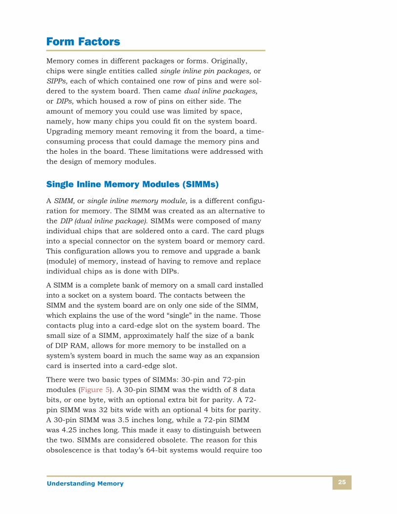
There were two basic types of SIMMs: 30-pin and 72-pin modules (Figure 5). A 30-pin SIMM was the width of 8 databits, or one byte, with an optional extra bit for parity. A 72-pin SIMM was 32 bits wide with an optional 4 bits for parity.A 30-pin SIMM was 3.5 inches long, while a 72-pin SIMM was 4.25 inches long. This made it easy to distinguish betweenthe two. SIMMs are considered obsolete. The reason for thisobsolescence is that today’s 64-bit systems would require too
Understanding Memory26
many SIMMs per bank. Even so, as a technician, you maycome across systems that contain SIMMs, so we’ll discussthem a little further.
Memory is typically added in four-bank increments, whichmeans you would need four 30-pin SIMMs or one 72-pinSIMM to upgrade a system. However, some systems thathave 486 processors may require two 72-pin SIMMs to be installed to make up a single bank. These systems useinterleaved memory, which means memory accesses arealternated between the SIMMs to improve performance.
All SIMMs in each bank must be the same capacity andspeed. If you wanted to add more memory, the four SIMMsockets in Bank 1 could be filled with 4 MB SIMMs. Thiswould give a total system memory of 20 MB.
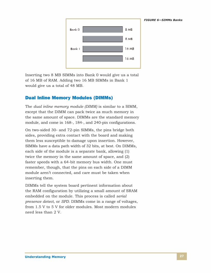
Imagine this is a Pentium Pro system board that uses 72-pinSIMMs. Since a Pentium uses 64-bit words, we would haveto install two SIMMs at a time to fill a bank (Figure 6).
FIGURE 5—SIMMs exist in 72- and 30-pin forms.
Professional TipCaution should be taken when adding memory with 30-pin SIMMs.Don’t mix nine-chip and three-chip modules! Erratic operation ofthe computer can result.
Understanding Memory 27
Inserting two 8 MB SIMMs into Bank 0 would give us a totalof 16 MB of RAM. Adding two 16 MB SIMMs in Bank 1would give us a total of 48 MB.
Dual Inline Memory Modules (DIMMs)
The dual inline memory module (DIMM) is similar to a SIMM,except that the DIMM can pack twice as much memory inthe same amount of space. DIMMs are the standard memorymodule, and come in 168-, 184-, and 240-pin configurations.
On two-sided 30- and 72-pin SIMMs, the pins bridge bothsides, providing extra contact with the board and makingthem less susceptible to damage upon insertion. However,SIMMs have a data path width of 32 bits, at best. On DIMMs,each side of the module is a separate bank, allowing (1)twice the memory in the same amount of space, and (2)faster speeds with a 64-bit memory bus width. One mustremember, though, that the pins on each side of a DIMMmodule aren’t connected, and care must be taken wheninserting them.
DIMMs tell the system board pertinent information about the RAM configuration by utilizing a small amount of SRAMembedded on the module. This process is called serial presence detect, or SPD. DIMMs come in a range of voltages,from 1.5 V to 5 V for older modules. Most modern modulesneed less than 2 V.
FIGURE 6—SIMMs Banks
Understanding Memory28
Rambus RIMMs
RIMMs are fast memory modules that utilize a different archi-tecture than DIMMs. “RIMM” isn’t an acronym but a name.RIMMs currently run at 2.5 volts; modules are similar in sizeto DIMMs and have 184 pins. The multibank version can run32 banks that support up to four simultaneous transactions.This high speed creates extra heat that’s dissipated by alu-minum covers, called sheaths, over the RAM module. RDRAMsockets are interconnected in a series, meaning that emptysockets have to be filled with continuity RIMMS (CRIMMS) tocomplete the circuit. As noted previously, RIMMs are now obso-lete, except for specialized applications.
Small Outline DIMMs (SO-DIMMs) and RIMMs (SO-RIMMs)
SO-DIMMs are a smaller version of DIMMs used primarily forlaptop or notebook computers. They come in pin sizes 144,200, or 204. The transfer rate is 64 bits. SO-DIMMs, despitetheir smaller size, are generally equal in power, voltage andcapacity to many full-sized DIMMs.
Professional TipWhen installing memory, note that module pins come in tin orgold, and that the same metal type as the socket should always be used.

Understanding Memory 29
Self-Check 21. Name two ways a SIMM and DIMM are alike. Name two ways they’re different.
__________________________________________________________
2. How many pins are on a DIMM?
__________________________________________________________
3. What are the two possible numbers of pins on a SIMM?
__________________________________________________________
4. Name the two memory types that preceded SIMMs in PCs.
__________________________________________________________
Check your answers with those on page 31.

NOTES
Understanding Memory30
31
Self-Check 11. The ROM BIOS chip
2. BEDO memory is faster than EDO memory.
3. Unlike DRAM, SRAM doesn’t have capacitors that needrefreshing; therefore, row/column latency isn’t an issue.This drastically lowers access times and makes SRAMmuch faster than DRAM.
4. When parity discovers an error, it signals the entire system to shut down. ECC can detect and correct cer-tain errors without the OS or user even knowing it.
Self-Check 21. A SIMM and a DIMM both hold RAM and fit on the
system board in a memory slot. A SIMM doesn’t hold asmuch memory as a DIMM, is shorter, and generallyslower than a DIMM.
2. A DIMM has 168, 184, or 240 pins on the edge connector.
3. A SIMM has either 30 or 72 pins on its edge connector.
4. SIPPs, DIPs
Answers
Answers