Embed Size (px)
Citation preview
International Journal of ChemTech Research CODEN( USA): IJCRGG ISSN : 0974-4290
Vol.6 , No.1, pp 705-718, Jan-March 2014
Studies on the Physical Properties of three Potentially
important TCO Thin Films fabricated by a Simplified Spray
Technique under same Deposition conditions
N. Manjula, K. Usharani, A.R. Balu *, V.S. Nagarethinam
AVVM Sri Pushpam College, Poondi – 613 503, Thanjav ur Dt, Tamilnadu, India.
*Corres.author: [email protected] Ph: +91 9442846351
Abstract: Potentially important transparent conducting thin films comprising the oxides of Zn, Sn and Cd were prepared under same deposition parameter conditions by a simplified spray technique. Multiple diffraction peaks observed in all the films indicate their polycrystalline nature. XRD patterns revealed that ZnO films has hexagonal wurtzite structure with a preferential orientation along the (0 0 2) plane. SnO2 thin films has orthorhombic structure with a preferential orientation along the (0 2 1) plane while CdO film has face centered cubic structure with a preferential orientation along the (1 1 1) plane. The band gap values of ZnO, SnO2 and CdO thin films were found to be equal to 3.1, 3.45 and 2.38 eV respectively. Microstructural parameters such as strain, dislocation density and the number of crystallites were calculated for all the samples. Electrical resistivity values of ZnO, SnO2 and CdO thin films were found to be equal to 0.24 x 10² ohm-cm, 1.8 x 10⁻¹ ohm-cm and 1.013 x 10⁻³ ohm-cm respectively. All the films exhibit photo luminescent properties. Keywords: XRD; Strain; Electrical resistivity; Optical studies; Band gap energy; Crystal structure.
1. Introduction
Electrically conductive materials with high optical transmittance are key elements for thin film solar cells and display devices. Amongst them, transparent conductive oxides (TCOs), based on high band gap, degenerate semiconductors are mechanically hard and can withstand high temperatures [1]. Transparent conducting oxides have long been a subject of various investigations due to their unique physical properties and applications in commercial devices [2, 3]. TCOs such as cadmium oxide (CdO), zinc oxide (ZnO), indium oxide (In2O3), tin oxide (SnO2), etc. have been widely studied because of their use in optoelectronic devices. Due to their optical and electrical properties, TCOs are used in photovoltaic solar cells, phototransistors, liquid crystal displays, optical heaters, gas sensors, transparent electrodes and other optoelectronic devices [4]. In the last few years, thin films of Zn, In, Sn and Cd oxides have received considerable attention, mainly due to their important potential applications.
http://www.sphinxsai.com/framesphinxsaichemtech.htm
A.R. Balu et al /Int.J. ChemTech Res.2014,6(1),pp 705-718. 706
Zinc oxide is an n-type wide band gap degenerated like semiconductor where its conductivity can be controlled by thermal treatment or by adequate doping [5]. It has an optical band gap of about 3.3 eV [6]. ZnO is non toxic and stable under normal environmental conditions. It is a good candidate to substitute indium tin oxide and tin oxide films in conductive electrodes of amorphous silicon solar cells due to the high stability in hydrogen plasma [7]. Its transparency and conductivity prove that it is one of the promising candidate in a number of opto-electronic applications like energy windows, liquid crystal displays [8], solar cells, gas sensors, ultrasonic oscillators, transducers [9].
Tin oxide thin films are n-type semiconductors with high transparency and very good electrical conductivity. They have a high band gap of Eg = 3.7 – 4.0 eV with tetragonal ructile structure, plasma frequency in the IR region and when suitably doped can be used both as a p-type and n-type semiconductor. Other than the high transparency and high conduction, the advantage of SnO2 film is high chemical stability even at high temperature and also they have the refractive index in the range 1.9 – 2, which makes them suitable for antireflection coatings. As a wide gap semiconductor, SnO2 films are known to have a wide range of technological applications such as transparent conducting electrodes, dye-sensitized solar cells [10, 11] and chemical sensors [12, 13] and now they seem to be more attractive for their luminescent properties [14, 15].
CdO is an n-type semiconductor, with a direct band gap of 2.5 eV [16], and an indirect one experimentally equal to 1.98 eV [17]. CdO films show a high transparency in the visible region of solar spectrum, as well as low ohmic resistance. They exhibit metal-like charge transport behaviour with an exceptionally large carrier mobility [18] which is necessary for high conductivity TCO materials, especially when low free carrier absorbance is desired. CdO films have vast applications in many optoelectronic devices, phototransistors and diodes, transparent electrodes, sensors, etc based on their specific optical and electrical properties [19]. Further, doped with a group III or group VII elements CdO can achieve TCO properties comparable with the best performing and most widely used materials such as indium tin oxide (ITO), doped zinc oxide and doped tin oxide [20].
Several physical and chemical methods are already reported for the synthesis of transparent conducting films comprising the oxides of Zn, Sn and Cd [21 – 26]. Amongst the chemical methods used to fabricate TCO films, spray pyrolysis is comparatively simple, low cost and offers several other advantages [27] over the other methods. In the present work, a simplified spray technique using perfume atomizer is employed to coat transparent conducting films comprising the oxides of Zn, Sn and Cd. The use of perfume atomizer has some specific advantages over the conventional spray technique using spray gun assembly [28]: low cost, no need for carrier gas, fine atomization and improved wettability between the sprayed micro particles and loss of the precursor to the surroundings is almost nil.
2. Experimental Details
2.1 Fabrication of TCO Films
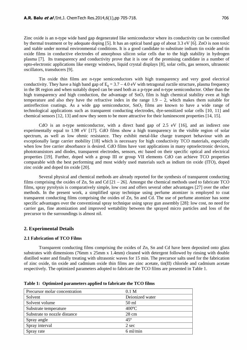
Transparent conducting films comprising the oxides of Zn, Sn and Cd have been deposited onto glass substrates with dimensions (76mm x 25mm x 1.4mm) cleaned with detergent followed by rinsing with double distilled water and finally treating with ultrasonic waves for 15 min. The precursor salts used for the fabrication of zinc oxide, tin oxide and cadmium oxide thin films are zinc acetate, tin(II) chloride and cadmium acetate respectively. The optimized parameters adopted to fabricate the TCO films are presented in Table 1.
Table 1: Optimized parameters applied to fabricate the TCO films
Precursor molar concentration 0.1 M Solvent Deionized water Solvent volume 50 ml Substrate temperature 400ºC Substrate to nozzle distance 28 cm Spray angle 45º Spray interval 2 sec Spray rate 6 ml/min
A.R. Balu et al /Int.J. ChemTech Res.2014,6(1),pp 705-718. 707
2.2 Characterization of TCO Films
The thicknesses of the TCO films were measured by means of weight gain method. X-ray diffraction patterns, SEM images, optical transmission and electrical resistivity values of the films were obtained using X-ray diffractometer (PANalytical – PW 340/60 X’pert PRO), Scanning electron microscope (HITACHI S-3000H), PerkinElmer UV-Vis-NIR double beam spectrophotometer (LAMBDA – 35), two probe technique for ZnO and SnO2 thin films and four point probe apparatus for CdO thin film respectively. X-ray diffractometer was operated at 40 kV and 30 mA with CuKα radiation of wavelength 1.54060 Å. Transmission spectra were recorded in the range 300 – 1100 nm.
The crystallite size is determined using the Scherrer formula:
cos
kD
λβ θ
= (1)
where β is the full width at half maximum (FWHM in radians) of the peak corrected for instrumental broadening, and θ is the Bragg angle.
The microstructural parameters such as strain (ε), dislocation density (δ) and number of crystallites (N) were determined by the formulae:
cos
4
β θε = (2)
2
1
Dδ = (3)
3
tN
D= (4)
The absorption coefficient (α) can be expressed by the relation:
( )n
gA h E
h
γα
γ−
= (5)
where A is a constant, Eg is the energy gap, γ is the frequency of the incident radiation and h is Planck’s constant. The exponent n is ½ for direct allowed transitions.
3. Results and Discussion
3.1 Film Formation Process
Aqueous solutions of the precursor salt viz. zinc acetate, tin (II) chloride and cadmium acetate were sprayed separately onto pre-heated glass substrates using a perfume atomizer. Each spray cycle has – a spray and a 2 sec wait so that the desired temperature is maintained throughout the deposition process. When the precursor solutions are sprayed over the hot substrates, pyrolytic decomposition takes place and colorless film of ZnO, white colored film of SnO2 and orange colored film of CdO are formed respectively. The thickness of the ZnO, SnO2 and CdO films were found to be equal to 0.241 µm, 0.6 µm and 0.893 µm respectively.
3.2 Structural Studies
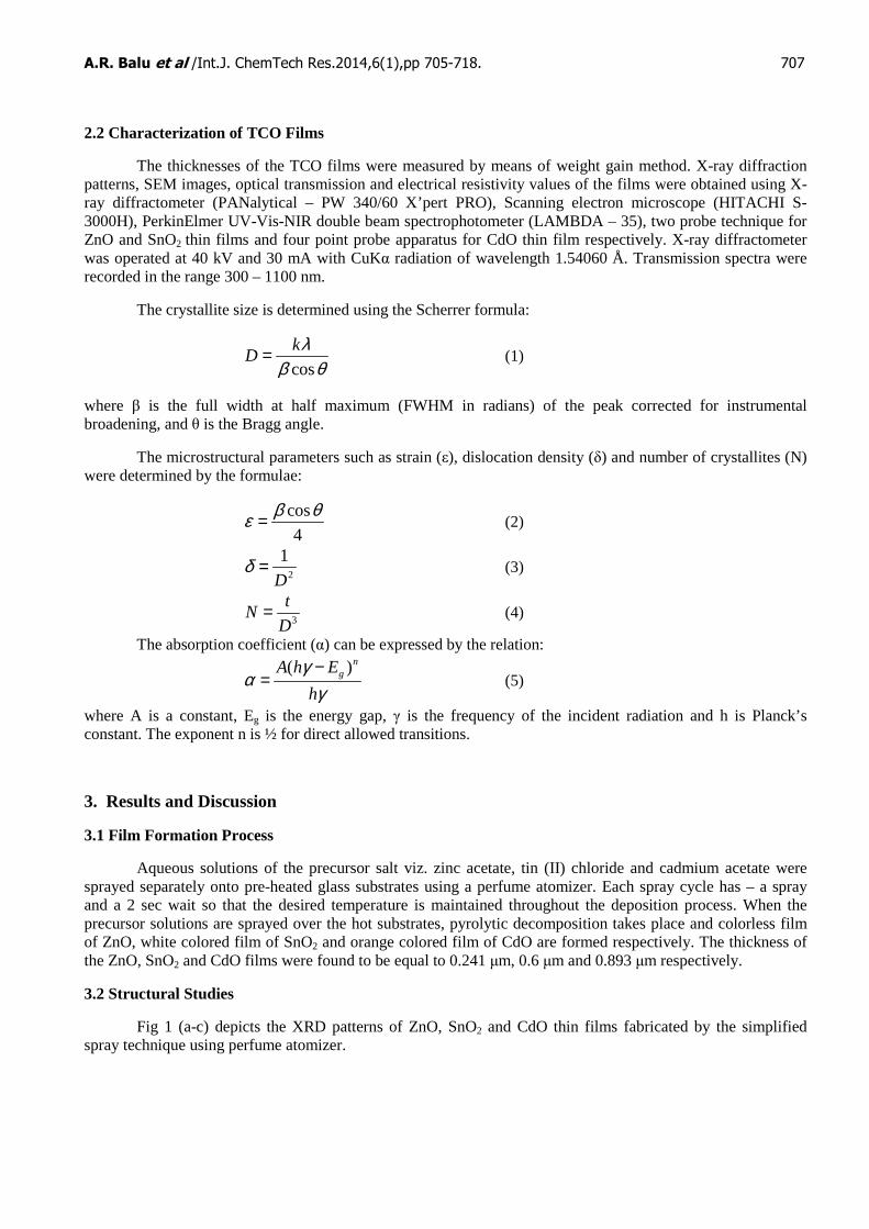
Fig 1 (a-c) depicts the XRD patterns of ZnO, SnO2 and CdO thin films fabricated by the simplified spray technique using perfume atomizer.
A.R. Balu et al /Int.J. ChemTech Res.2014,6(1),pp 705-718. 708
Fig 1 : XRD patterns of TCO thin films fabricated by the simplified spray technique.
Fig 1 (a)) shows the typical XRD patterns of ZnO thin films fabricated by the simplified spray technique. The XRD pattern revealed that the film is polycrystalline in nature with preferred (0 0 2) orientation together with (1 0 0), (1 0 1), (1 0 2), (1 1 0), (1 0 3) and (1 1 2) peaks. The position of the diffraction peaks fit well with the hexagonal wurtzite structure [JCPDS Card No. 36-1451]. The predominance of (0 0 2) plane clearly showed that the growth of the film is that the c-axis is perpendicular to the surface of the substrate. The result on preferred orientation in well agreed with several earlier reports [29, 30]. The lattice constants ‘a’ and ‘c’ for ZnO films are estimated using the relation [31]:
2 2 2
2 2 2
1 4 ( )
3
h hk k l
d a c
+ += + (6)
and the obtained values of a and c are 3.257 Å and 5.211 Å respectively. These values agree with the standard values [JCPDS card No. 36-1451].
Fig.(1(b)) shows the XRD pattern of SnO2 thin film fabricated by the simplified spray technique. The film is polycrystalline in nature with orthorhombic structure (JCPDS Card No.78-1063). It is perceptible from the figure that the as-deposited SnO2 film grow along the preferred orientation of (0 2 1) plane. Presence of other orientations such as (2 0 0),(1 2 5),(0 2 8) and (0 4 2) have also been detected. Traces of SnO phase are also observed with the presence of (1 1 0) and (1 1 3) peaks (JCPDS Card No. 72 – 2324). The presence of SnO phase in tin oxide thin films has been reported earlier [32, 33]. The lattice constants ‘a’, ‘b’ and ‘c’ corresponding to orthorhombic structure of SnO2 films was evaluated using the relation [31]:
2 2 2
2 2 2 2
1 h k l
d a b c= + + (7)
The values of the lattice constants were found to be equal to a = 4.737 Å, b = 5.708 Å and c = 15.875 Å respectively. These values agree well with the standard values (JCPDS Card No. 78 – 1063).

A.R. Balu et al /Int.J. ChemTech Res.2014,6(1),pp 705-718. 709
Different peaks in the XRD pattern of CdO film (Fig 1(c)) appeared at 2θ values 33.03º, 38.34º, 55.3º, 66º and 69.4º due to reflection from (1 1 1), (2 0 0), (3 1 1) and (2 2 2) planes respectively of CdO. The relatively stronger intensity of the peak at 2θ = 33.03º indicates preferential (1 1 1) orientation of the film (JCPDS Card No. 5 - 0640) and similar behavior has also been reported by others [34, 28]. XRD pattern also reveals that CdO has face centered cubic (FCC) structure with a lattice parameter equal to 4.692Å. The obtained ‘a’ value is in good agreement with other results [35]. The comparison of standard and observed d-spacing values of the TCO films is presented in Table 2.
The crystallite size and the microstructural parameters such as strain, dislocation density and number of crystallites of the TCO films were calculated using equations (1 – 4) and the obtained values are presented in Table 3.
Table 2: Comparison of standard and observed d-spacing values of TCO thin films
Std. – Standard Obs. - Observed a JCPDS Card No. 36 - 1451 b JCPDS Card No. 78 – 1063 (Orthorhombic SnO2) c JCPDS Card No. 72 – 2324 (Orthorhombic SnO) d JCPDS Card No. 5 - 0640 Table 3: Microstructural parameters of the TCO films fabricated by the simplified spray technique
3.3 Electrical Studies
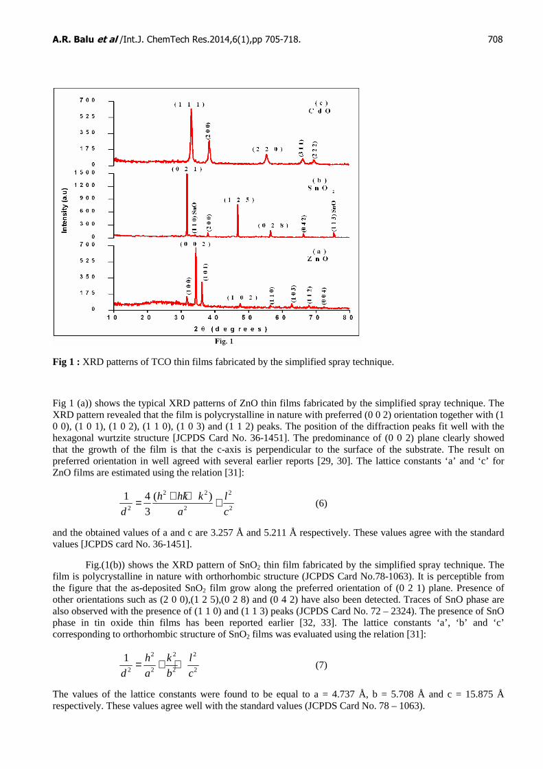
Electrical resistivity (ρ) of ZnO and SnO2 thin films were measured by two probe technique and that of CdO films by four point probe method. Fig 2 shows the variation of resistivity with temperature of the TCO films fabricated by the simplified spray technique.
ZnO SnO2 CdO d – spacing values
d – spacing values d – spacing values
Stda Obs. (h k l)
Std.b & c Obs. (h k l)
Std.d Obs. (h k l)
2.8143 2.8178 (1 0 0) 2.8089 2.817 (0 2 1) 2.712 2.709 (1 1 1) 2.6055 2.6055 (0 0 2) c2.6237 2.623 (1 1 0) 2.349 2.346 (2 0 0) 2.4759 2.4792 (1 0 1) 2.3685 2.370 (2 0 0) 1.661 1.660 (2 2 0) 1.9111 1.9125 (1 0 2) 1.9365 1.993 (1 2 5) 1.416 1.414 (3 1 1) 1.6247 1.6278 (1 1 0) 1.6285 1.627 (0 2 8) 1.355 1.353 (2 2 2) 1.4771 1.4783 (1 0 3) 1.4044 1.409 (0 4 2) --- --- --- 1.3781 1.3788 (1 1 2) c1.2578 1.261 (1 1 3) --- --- ---
Microstructural parameters ZnO SnO2 CdO Crystallite size, D (nm) 52 107 17 Strain, ε x 10-3 2.26 1.18 7.36 Dislocation density, δ x 1015 3.701 8.684 3.6412 Number of crystallites, N x 1015
1.714 0.49 0.02
A.R. Balu et al /Int.J. ChemTech Res.2014,6(1),pp 705-718. 710
Fig 2 : Variation of electrical resistivity with temperature of ZnO, SnO2 and CdO thin films
The resistivity of all the films decreases with increase in temperature indicating the semiconducting nature of these films. The average resistivity of ZnO, SnO2 and CdO thin films measured in the temperature range of 308 K – 353 K were found to be equal to 0.24 x 10² ohm-cm, 1.8 x 10⁻¹ ohm-cm and 1.351 x 10⁻³ ohm-cm respectively. In thin films, resistivity depends on film thickness. In bulk the resistance to the charge carriers is usually caused by photon scattering, impurity and defect scattering. In additional there is scattering from the film surface itself. The surface scattering decreases with increase in film thickness and is negligible if the film thickness is greater than the electron mean free path in the bulk [36].
Amanullah et al. [37] obtained a resistivity of 0.77 x 10⁻² ohm-cm for SnO2 film with thickness 130.6 nm. They reported that resistivity of tin oxide films decreases with increase in film thickness due to dominance of surface scattering. As film thickness increases surface scattering decreases with consequent reduction in the resistivity of the films. Tin oxide film obtained in this work has a thickness of 600 nm which is very much greater than 130.6 nm. Hence the resistivity obtained here is decreased nearly by one order due to negligible surface scattering.
Lamb et al. [38] obtained a resistivity of 2.3 x 10⁻³ ohm-cm for the CdO films with thickness 546 nm by metal organic chemical vapour deposition at 372ºC. In this work, the substrate temperature maintained to fabricate CdO film is 400ºC which is slightly higher than 372ºC maintained by Lamb et al., and the thickness of the CdO film obtained is 892.8 nm. Even though the film thickness is higher than that obtained by Lamb et al., a low resistivity value (1.013 x 10⁻³ ohm-cm) is achieved here. The low resistivity value obtained here can be attributed to the decreased potential barrier between grains due to the elimination of a number of charge centers located at the grain boundaries, due to high substrate temperature; or the formation of vacancies of oxygen in the structure of the material [39].
The resistivity of sprayed ZnO thin films is strongly influenced by the following factors [40]: i) interstitial incorporation of zinc and ii) presence of oxygen vacancies. The low value of resistivity obtained for the ZnO film in this work can be attributed to the desorption of oxygen at grain boundaries [41] which act as traps for electrons. The value of resistivity obtained exactly matches with the value reported earlier [42].
From the resistance values recorded at different temperatures, the temperature coefficient of resistance (TCR) of the TCO films is evaluated. The TCR values of ZnO, SnO2 and CdO thin films were found to be equal to -2.96 x 10⁻³ / K, -3.25 x 10⁻³ / K and -1.328 x 10⁻³ / K respectively. The values obtained confirm that all the films have good heat resistance property, which is one of the desirable qualities for solar cell TCO layers [43]. The magnitude of TCR of the CdO film is remarkably lesser than ZnO and SnO2 films, which concludes that CdO film fabricated in this work has better thermal stability than ZnO and SnO2 films.
A.R. Balu et al /Int.J. ChemTech Res.2014,6(1),pp 705-718. 711
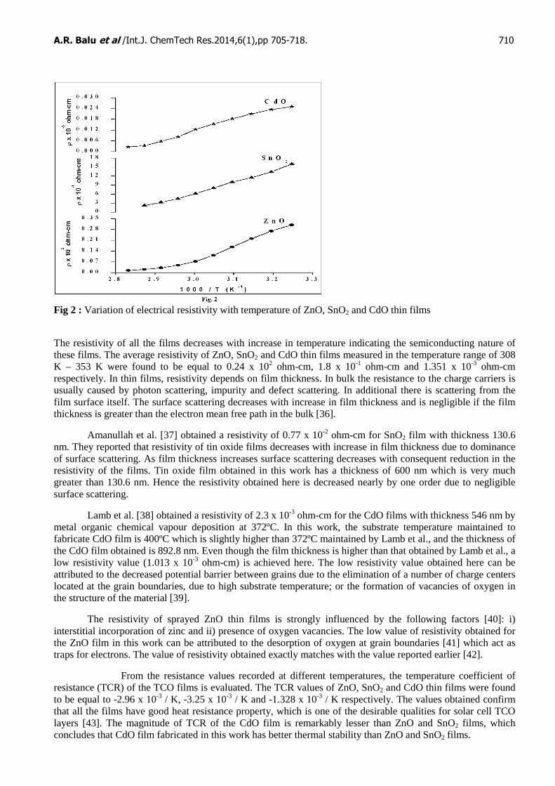
3.4 Surface Morphological Studies
The SEM images of the TCO films fabricated by the simplified spray technique are shown in Fig. 3. Nanosized grass like structures was observed on the SEM image of ZnO thin film (Fig. 3(a)).
The nanorods show no alignment and are dispersively distributed, but their diameters and lengths are rather uniform. The surface also contains polyhedral shells distributed dispersively on the substrate, with some of them line up along the nanorods. The SEM image of SnO2 thin film (Fig. 3(b)) show small granular grains distributed throughout the surface without any cracks.
However white colored patches appeared here and there on the film surface which might be due to the incomplete decomposition of the precursor salt used. The SEM image of the CdO film (Fig. 3(c)) is composed of clusters of spherical grains with size equal to 64 nm.
Fig 3 : SEM images of the as-deposited TCO films.
Film surface appears to be uniform with no holes or cracks. Grains appear to be interconnected without any holes or devoids.
3.5 Optical Studies
Fig. 4 shows the optical transmission and reflection spectra of the TCO films prepared by the simplified spray technique under same deposition conditions.
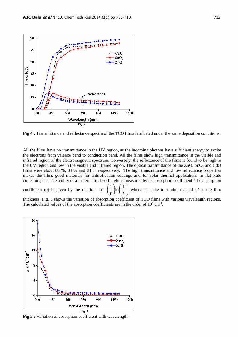
A.R. Balu et al /Int.J. ChemTech Res.2014,6(1),pp 705-718. 712
Fig 4 : Transmittance and reflectance spectra of the TCO films fabricated under the same deposition conditions.
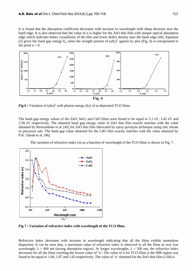
All the films have no transmittance in the UV region, as the incoming photons have sufficient energy to excite the electrons from valence band to conduction band. All the films show high transmittance in the visible and infrared region of the electromagnetic spectrum. Conversely, the reflectance of the films is found to be high in the UV region and low in the visible and infrared region. The optical transmittance of the ZnO, SnO2 and CdO films were about 88 %, 84 % and 84 % respectively. The high transmittance and low reflectance properties makes the films good materials for antireflection coatings and for solar thermal applications in flat-plate collectors, etc. The ability of a material to absorb light is measured by its absorption coefficient. The absorption
coefficient (α) is given by the relation: 1 1
lnt T
α =
where T is the transmittance and ‘t’ is the film
thickness. Fig. 5 shows the variation of absorption coefficient of TCO films with various wavelength regions. The calculated values of the absorption coefficients are in the order of 104 cm-1.
Fig 5 : Variation of absorption coefficient with wavelength.
A.R. Balu et al /Int.J. ChemTech Res.2014,6(1),pp 705-718. 713
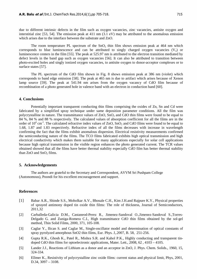
It is found that the absorption coefficient decreases with increase in wavelength with sharp decrease near the band edge. It is also observed that the value of α is higher for the ZnO thin film with steeper optical absorption edge which indicates better crystallinity of the film and lower defect density near the band edge [44]. Equation (5) gives the band gap energy Eg when the straight portion of (αhγ)2 against hγ plot (Fig. 6) is extrapolated to the point α = 0.
Fig 6 : Variation of (αhγ)2 with photon energy (hγ) of as-deposited TCO films.
The band gap energy values of the ZnO, SnO2 and CdO films were found to be equal to 3.1 eV, 3.45 eV and 2.38 eV respectively. The obtained band gap energy value of ZnO thin film exactly matches with the value obtained by Benramdane et al. [45] for ZnO thin film fabricated by spray pyrolysis technique using zinc nitrate as precursor salt. The band gap value obtained for the CdO film exactly matches with the value obtained by P.K. Ghosh et al. [46].
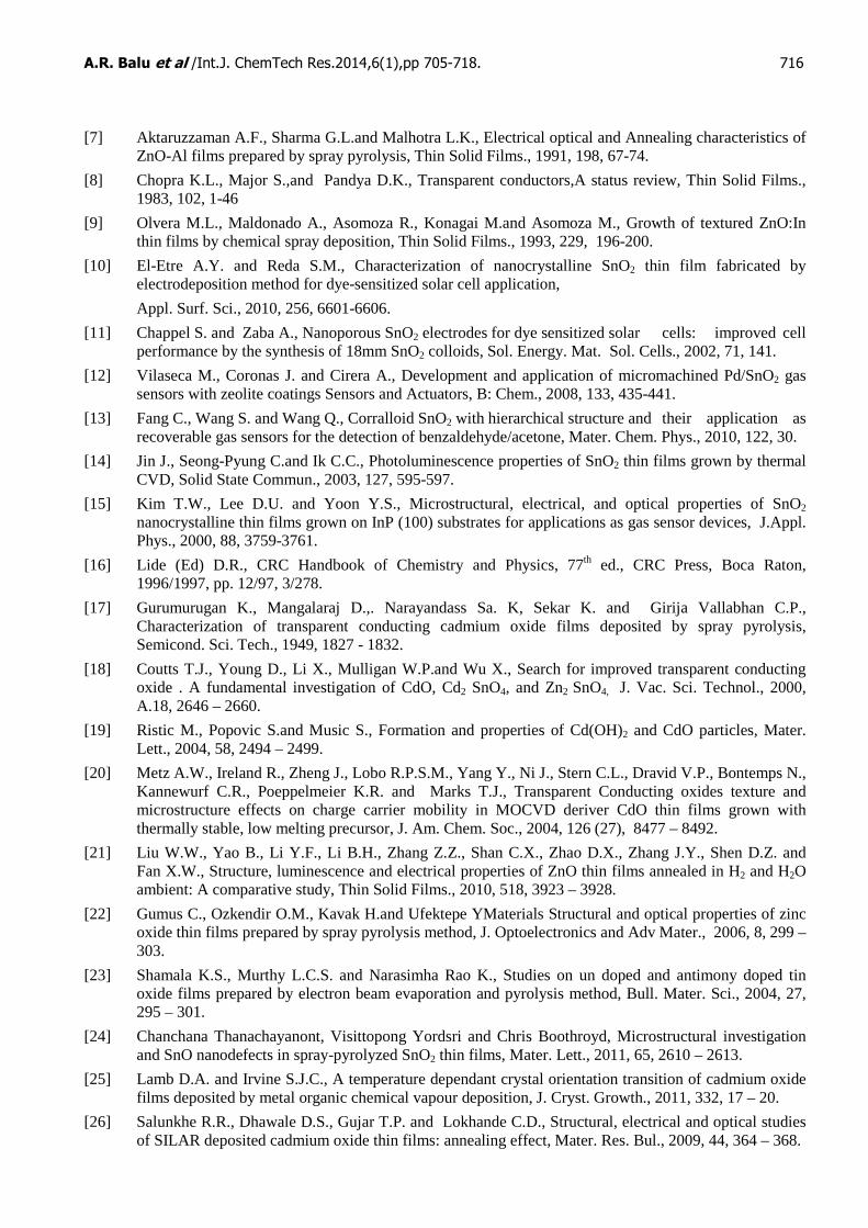
The variation of refractive index (n) as a function of wavelength of the TCO films is shown in Fig. 7.
Fig 7 : Variation of refractive index with wavelength of the TCO films.
Refractive index decreases with increase in wavelength indicating that all the films exhibit anomalous dispersion. It can be seen that, a maximum value of refractive index is observed in all the films at very low wavelength, λ ≈ 400 nm (strong absorption region). At longer wavelengths, λ > 500 nm, the refractive index decreases for all the films reaching the lowest value of ‘n’. The value of n for TCO films is the NIR region was found to be equal to 1.68, 1.87 and 1.83 respectively. The value of ‘n’ obtained for the ZnO thin film (1.68) is

A.R. Balu et al /Int.J. ChemTech Res.2014,6(1),pp 705-718. 714
lower than the value 1.89 obtained by Vindokumar et al. [47] for laser ablated nanostructured ZnO films annealed at 500ºC. The value of ‘n’ obtained for the SnO2 film (1.87) exactly matches with the value obtained by Shamala et al. [23] for tin oxide thin films prepared by electron beam evaporation technique. The value of ‘n’ obtained for SnO2 thin film makes them suitable for antireflection coatings. The value of ‘n’ obtained for CdO thin film (1.83) is slightly lower than the value obtained my Mohamed et al. [48] for CdO buffer layer formed by electron beam evaporation technique.
In many applications requiring transparent conducting films, the optical transmission and electrical conductivity should be as high as possible. This is particularly important for solar cell applications because high optical transmission in the visible region enhances the photo generated current and low sheet resistance reduces the series resistance of the cell. The interrelationship between transmission and conductivity is expressed by the figure of merit (ф). When the sheet resistance (Rsh) and the optical transmission (T) are known, the figure of merit is calculated by using the formula [49] :
10
sh
T
Rφ = (8)
The figure of merit values calculated for ZnO, SnO2 and CdO thin films were found to be equal to 2.46 x 10⁻⁹ Ω-
1, 8.314 x 10⁻⁷ Ω-1 and 6.26 x 10⁻³ Ω-1 respectively. The value of φ obtained for ZnO thin film is very low which might be due to high value of sheet resistance (0.175 x 10¹⁰ ohm/sq.) obtained. The value of φ obtained for SnO2 thin film exactly matches with the value obtained by Manifacier et al. [50] for tin oxide film fabricated by vacuum flash evaporation method. The figure of merit value obtained for the CdO film exactly matches with the value obtained in our earlier work [28].
3.6 Photoluminescence Studies
The room temperature photoluminescence spectra of the TCO films fabricated by the simplified spray technique are shown in Fig. 8.
Fig 8 : PL spectra of the TCO films. The PL spectra of ZnO thin film shows emission peaks at 2.17 eV and at 2.81 eV which corresponds to interstitial zinc or surface defects due to oxygen vacancies [51, 52]. The peaks observed at 521 nm, 544 nm and 571 nm shows that the film exhibits a deep green emission. It is reported that the green emission in ZnO can be
A.R. Balu et al /Int.J. ChemTech Res.2014,6(1),pp 705-718. 715
due to different intrinsic defects in the film such as oxygen vacancies, zinc vacancies, antisite oxygen and interstitial zinc [53, 54]. The emission peak at 411 nm (3.1 eV) may be attributed to the anomalous emission which arises due to the interface between the substrate and ZnO.
The room temperature PL spectrum of the SnO2 thin film shows emission peak at 464 nm which corresponds to blue luminescence and can be attributed to singly charged oxygen vacancies (Vo) or luminescence centers in the film [55]. The peak at 525.97 nm is attributed to the electron transition mediated by defect levels in the band gap such as oxygen vacancies [56]. It can also be attributed to transition between photo-excited holes and singly ionized oxygen vacancies, to antisite oxygen to donor-acceptor complexes or to surface states [57].
The PL spectrum of the CdO film shown in Fig. 8 shows emission peak at 386 nm (violet) which corresponds to band edge emission [58]. The peak at 465 nm is due to artifact which arises because of Xenon lamp source [59]. The peak at 541.94 nm arises from the oxygen vacancy of CdO film because of recombination of a photo generated hole in valence band with an electron in conduction band [60].
4. Conclusions
Potentially important transparent conducting thin films comprising the oxides of Zn, Sn and Cd were fabricated by a simplified spray technique under same deposition parameter conditions. All the film was polycrystalline in nature. The transmittance values of ZnO, SnO2 and CdO thin films were found to be equal to 84 %, 84 % and 88 % respectively. The calculated values of absorption coefficient for all the films are in the order of 104 cm-1. The calculated refractive index values of ZnO, SnO2 and CdO films were found to be equal to 1.68, 1.87 and 1.83 respectively. Refractive index of all the films decreases with increase in wavelength confirming the fact that the films exhibit anomalous dispersion. Electrical resistivity measurements confirmed the semiconducting nature of the films. The TCO films fabricated exhibits high optical transmission and high electrical conductivity which makes them suitable for many applications especially for solar cell applications because high optical transmission in the visible region enhances the photo generated current. The TCR values obtained showed that all the films have better thermal stability especially CdO film has better thermal stability than ZnO and SnO2 films.
5. Acknowledgements
The authors are grateful to the Secretary and Correspondent, AVVM Sri Pushpam College (Autonomous), Poondi for his excellent encouragement and support.
References [1] Babar A.R., Shinde S.S., Moholkar A.V., Bhosale C.H., Kim J.H.and Rajpure K.Y., Physical properties
of sprayed antimony doped tin oxide thin films: The role of thickness, Journal of Semiconductors, 2011,32
[2] Carballeda-Galicia D.M., Castaneod-Perez R., Jimenez-Sandoval O.,Jimenez-Sandoval S.,Torres-Delgado G. and Zuniga-Romera C.I., High transmittance CdO thin films obtained by the sol-gel method, Thin Solid Films, 2000, 371, 105-108.
[3] Caglar Y., Ilican S. and Caglar M., Single-oscillator model and determination of optical constants of spray pyrolyzed amorphous SnO2 thin films, Eur. Phys. J,.2007, B. 58, 251-256.
[4] Gupta R.K., Ghosh K., Patel R., Mishra S.R. and Kahol P.K., Highly conducting and transparent tin-doped CdO thin films for optoelectronic applications, Mater. Lett., 2008, 62 , 4103 – 4105.
[5] Lander J.J., Reactions of Lithium as a donor and an acceptor in ZnO, J. Phys. Chem. Solids., 1960, 15, 324-334.
[6] Ellmer K., Resistivity of polycrystalline zinc oxide films: current status and physical limit, Phys, 2001, D.34, 3097 – 3108.
A.R. Balu et al /Int.J. ChemTech Res.2014,6(1),pp 705-718. 716
[7] Aktaruzzaman A.F., Sharma G.L.and Malhotra L.K., Electrical optical and Annealing characteristics of
ZnO-Al films prepared by spray pyrolysis, Thin Solid Films., 1991, 198, 67-74.
[8] Chopra K.L., Major S.,and Pandya D.K., Transparent conductors,A status review, Thin Solid Films., 1983, 102, 1-46
[9] Olvera M.L., Maldonado A., Asomoza R., Konagai M.and Asomoza M., Growth of textured ZnO:In thin films by chemical spray deposition, Thin Solid Films., 1993, 229, 196-200.
[10] El-Etre A.Y. and Reda S.M., Characterization of nanocrystalline SnO2 thin film fabricated by electrodeposition method for dye-sensitized solar cell application,
Appl. Surf. Sci., 2010, 256, 6601-6606.
[11] Chappel S. and Zaba A., Nanoporous SnO2 electrodes for dye sensitized solar cells: improved cell performance by the synthesis of 18mm SnO2 colloids, Sol. Energy. Mat. Sol. Cells., 2002, 71, 141.
[12] Vilaseca M., Coronas J. and Cirera A., Development and application of micromachined Pd/SnO2 gas sensors with zeolite coatings Sensors and Actuators, B: Chem., 2008, 133, 435-441.
[13] Fang C., Wang S. and Wang Q., Corralloid SnO2 with hierarchical structure and their application as recoverable gas sensors for the detection of benzaldehyde/acetone, Mater. Chem. Phys., 2010, 122, 30.
[14] Jin J., Seong-Pyung C.and Ik C.C., Photoluminescence properties of SnO2 thin films grown by thermal CVD, Solid State Commun., 2003, 127, 595-597.
[15] Kim T.W., Lee D.U. and Yoon Y.S., Microstructural, electrical, and optical properties of SnO2 nanocrystalline thin films grown on InP (100) substrates for applications as gas sensor devices, J.Appl. Phys., 2000, 88, 3759-3761.
[16] Lide (Ed) D.R., CRC Handbook of Chemistry and Physics, 77th ed., CRC Press, Boca Raton, 1996/1997, pp. 12/97, 3/278.
[17] Gurumurugan K., Mangalaraj D.,. Narayandass Sa. K, Sekar K. and Girija Vallabhan C.P., Characterization of transparent conducting cadmium oxide films deposited by spray pyrolysis, Semicond. Sci. Tech., 1949, 1827 - 1832.
[18] Coutts T.J., Young D., Li X., Mulligan W.P.and Wu X., Search for improved transparent conducting oxide . A fundamental investigation of CdO, Cd2 SnO4, and Zn2 SnO4, J. Vac. Sci. Technol., 2000, A.18, 2646 – 2660.
[19] Ristic M., Popovic S.and Music S., Formation and properties of Cd(OH)2 and CdO particles, Mater. Lett., 2004, 58, 2494 – 2499.
[20] Metz A.W., Ireland R., Zheng J., Lobo R.P.S.M., Yang Y., Ni J., Stern C.L., Dravid V.P., Bontemps N., Kannewurf C.R., Poeppelmeier K.R. and Marks T.J., Transparent Conducting oxides texture and microstructure effects on charge carrier mobility in MOCVD deriver CdO thin films grown with thermally stable, low melting precursor, J. Am. Chem. Soc., 2004, 126 (27), 8477 – 8492.
[21] Liu W.W., Yao B., Li Y.F., Li B.H., Zhang Z.Z., Shan C.X., Zhao D.X., Zhang J.Y., Shen D.Z. and Fan X.W., Structure, luminescence and electrical properties of ZnO thin films annealed in H2 and H2O ambient: A comparative study, Thin Solid Films., 2010, 518, 3923 – 3928.
[22] Gumus C., Ozkendir O.M., Kavak H.and Ufektepe YMaterials Structural and optical properties of zinc oxide thin films prepared by spray pyrolysis method, J. Optoelectronics and Adv Mater., 2006, 8, 299 – 303.
[23] Shamala K.S., Murthy L.C.S. and Narasimha Rao K., Studies on un doped and antimony doped tin oxide films prepared by electron beam evaporation and pyrolysis method, Bull. Mater. Sci., 2004, 27, 295 – 301.
[24] Chanchana Thanachayanont, Visittopong Yordsri and Chris Boothroyd, Microstructural investigation and SnO nanodefects in spray-pyrolyzed SnO2 thin films, Mater. Lett., 2011, 65, 2610 – 2613.
[25] Lamb D.A. and Irvine S.J.C., A temperature dependant crystal orientation transition of cadmium oxide films deposited by metal organic chemical vapour deposition, J. Cryst. Growth., 2011, 332, 17 – 20.
[26] Salunkhe R.R., Dhawale D.S., Gujar T.P. and Lokhande C.D., Structural, electrical and optical studies of SILAR deposited cadmium oxide thin films: annealing effect, Mater. Res. Bul., 2009, 44, 364 – 368.
A.R. Balu et al /Int.J. ChemTech Res.2014,6(1),pp 705-718. 717
[27] Hiie J., Dedova T., Valdna V. and Muska K., Comparative study of nanostructured CdS thin films prepared by CBD and spray pyrolysis: Annealing effect, Thin Solid Films., 2006, 511 –512, 443 - 447.
[28] Usharani K., Balu A.R., Shanmugavel G., Suganya M.and Nagarethinam V.S., Transparent Conducting CdO thin films fabricated by low cost simplified spray technique using perfume atomizer, International. J. Sci. Res. Rev., 2013, 2(3), 53 – 68.
[29] Rozati S.M., Moradi S., Golshahi S., Martins R. and Fortunato E., Electrical, structural and optical properties of fluorine doped zinc oxide thin films: Effect of the solution aging time, Thin Solid Films., 2009, 518, 1279 - 1288.
[30] Kumar P.M.R., Kartha C.S., Vijayakumar K.P., Singh F. and Avasthi D.K., On the properties of indium doped ZnO thin films, Semicond. Sci. Technol., 2005, 20, 120-126.
[31] Cullity B.D., Elements of X-ray Diffraction, Addison-Wesley Publishing Company, 1978.
[32] Leja E., Korecki J., Krop K. and Toll K., Phase composition of SnOx thin films obtained by reactive d.c. sputtering, Thin Solid Films., 1979, 59, 147-155.
[33] Murthy N.S. and Jewalekar S.P., Phase conjugation in an amorphous As2S3 thin films, Thin Solid Films., 1979, 90, 147.
[34] Saha B., Das S.and Chottopadhyay K.K., Electrical and optical properties of Al doped cadmium oxide thin films deposited by radio frequency magnetron sputtering, Sol.Energy.Mater.Sol.Cells., 2007, 91,1692.
[35] Subramanyam T.K., Uthanna S.and Srinivasulu Naidu B., Preparation and characterization of CdO films deposited by dc magnetron reactive sputtering, Materials Letters., 1998,.35, 214 - 220.
[36] Berry R.W., Hall P.M. and Haris M.T., Thin Film Technology, Van Nostrand Reinbold Company, NY, 1968, p. 310.
[37] Amanullah F.M., Saleh Al-Mobarak M., Al-Dhafiri A.M. and Al-Shibani K.M., Development of spray technique for the preparation of thin films and characterization of tin oxide transparent conductors, Mat. Chem. Phys., 1999, 59, 247 – 253.
[38] Lamb D.A. and Irvine S.J.C., A temperature dependent orientation transition of cadmium oxide films deposited by metal organic chemical vapour deposition, J. Cryst. Growth., 2011, 332, 17 – 20.
[39] Ghosh P.K., Maity R. and Chattopadhyay K.K., Electrical and optical properties of highly conducting CdO:F thin film deposited by sol–gel dip coating technique
Sol. Energy, Mater. Sol. Cells., 2004, 81, 279 - 289 .
[40] Goyal D.J., Agashe C.M., Marathe B.R., Takwale M.G.and Bhinde V.G., Effect of precursor solution concentration on the structural properties of sprayed ZnO films, J. Mater. Sci. Lett, 1992,11, 708 – 710.
[41] Major S., Banerjee A. and Chopra K.L., Annealing studies of undoped and indium doped films of zinc oxide, Thin Solid Films., 1984, 41, 154.
[42] Nunes P., Fernandes B., Fortunato E., Vilarinho P. and Martins R., Performances presented by zinc oxide thin films deposited by spray pyrolysis, Thin Solid Films., 1999, 337, 176 – 179.
[43] Fukano T. and Motohiro T., Low temperature growth of highly crystallized transparent conductive fluorine doped tin oxide films by intermittent spray pyrolysis deposition, Sol. Energy. Mater. Sol. Cells., 2004, 82, 567.
[44] Malle Krunks. and Enn Mellikov, Zinc oxide thin films by spray pyrolysis method, Thin Solid Films., 1995, 278, 33.
[45] Benramdane N., Murad, W.A., Misho R.H., Ziane M. and Kebbab Z., A chemical method for the preparation of thin films of CdO and ZnO, Mater. Chem. Phys., 48 (1997) 119 – 123.
[46] Ghosh P.K., Maity R. and Chattopadhyay K.K., Electrical and optical properties of highly conducting CdO:F thin film deposited by sol–gel dip coating technique, Sol. Energy, Mater. Sol. Cells., 2004, 81, 279 - 289.
[47] Vinodkumar R., Lethy K.J., Arunkumar P.R., Renju Krishnan R., Venugopalan Pillai N., Mahadevan Pillai V.P. and Reji Philip., Effect of cadmium oxide incorporation on the microstructural and optical properties of pulsed laser deposited nanostructured zinc oxide thin films, Mater. Chem. Phys., 2010, 121, 406 – 413.

A.R. Balu et al /Int.J. ChemTech Res.2014,6(1),pp 705-718. 718
[48] Mohamed H.A. and Mahmoud Ali H., Characterization of ITO/CdO/glass thin films evaporated by electron beam technique, Sci. Technol. Adv. Mater., 2008, 9, 025016.
[49] Haacke G., New figure of merit for transparent conductors, J. Appl.Phys,1976, 47, 4086 - 4089.
[50] Manifacier J.C., Fillard P. and Bind J.M., Deposition of In2O3 – SnO layers on glass, Thin Solid Films, 1981, 77, 67.
[51] Girgis S.Y., Salem A.M.and Selim M.S., Structural characterization and refractive index dispersion analysis of HgSe thin films grown by reactive solutions, J. Phys. Condensed. Matter, 2007, 19, 116213
[52] Rani J.R., Mahadevan Pillai V.P., Ajimsha R.S., Jayaraj M.K.and Jayasree R.S., Effect of substrate roughness on photoluminescence spectra of silicon nanocrystals grown by off axis pulsed laser deposition, J. Appl. Phys, 2006, 100, 014302.
[53] Shonoya S.and Yen (Eds.) W.M., Phosphor Handbook, Chemical Rubber Cleveland, 1999.
[54] Studenikis S.A.and Cocivera M., Time-resolved luminescence and photoconductivity of polycrystalline ZnO films, J. Appl. Phys, 2002, 91, 5060-5065.
[55] Rani S., Roy S.C.and Karar N., Structure, microstructure and photoluminescence properties of Fe doped SnO2 thin films, Solid State Commun, 2007,141, 214.
[56] Gaidi M., Hajjaji A., Smirani R., Bessais B. and El Khakani M.A., Structure and photoluminescence of ultra thin films of SnO2 nanoparticles synthesized by means of pulsed laser deposition, J. Appl. Phys, 2010, 108, 063537.
[57] Lettieri S., Bismuto A., Maddalena P., Barattob C., Comini E., Faglia G., Sberveglieri G.and Zanotti L., Gas sensitivie light emission properties of tin oxide and zinc oxide nanobelts, J. Nanocrystalline solids, 2006, 352, 1457 – 1460.
[58] Ningthoujam R.S., Sudarsan V.and Kulshreshtha S.K., SnO2:Eu nanoparticles dispersed in silica: A low temperature synthesis and photoluminescence study, J. Lumin, 2007,127, 747.
[59] Lanje A.S., Ningthoujam R.S., Sharma S.J.and Pode R.B., Luminescence and electrical resistivity properties of cadmium oxide nanoparticles, Indian. J. Pure. & Appl. Physics, 2011, 49, 234 – 238.
[60] Ningthoujam R.S., Lahiri D., Sudarsan V., Poswal H., Kulshreshtha S.K., Sharma S.M., Bhushan B., Sastry M.D., Nature of Vn+ ions in SnO2: An EPR and photoluminescence study, Mater. Res. Bull, 2007, 42, 1294.
*****