Embed Size (px)
Citation preview
STM32L4
Analog Peripheral
Analog-to-digital converter (ADC)
ADC Features (1/2) 2
02/07/2015 Presentation Title
• Up to 3 ADCs:
• ADC1 & ADC2 are tightly coupled and can operate in dual mode (ADC1 is master)
• ADC3 is standalone, but it share the interface with ADC1 & 2
• Programmable Conversion resolution : 12, 10, 8 or 6 bit• Low power design
• Consumption linear vs. conversion rate : 200 µA / MSps
• ADC speed independent from CPU frequency (dual clock architecture)
• ADC conversion time:• Fast channels : up to 5.3Ms/s with 12 bit resolution in single mode• Slow channels: up to 4.8Ms/s with 12 bit resolution in single mode
• Channel-wise programmable sampling time• External Analog Input Channels for each of the 3 ADCs:
• 5 fast channels from dedicated GPIOs pads• Up to 11 slow channels from dedicated GPIOs pads
• Can manage Single-ended or differential inputs• Self-calibration
ADC Features (2/2) 3
02/07/2015 Presentation Title
• 5 internal channels connected to :
• Temperature sensor Vsense connected to ADC1 and ADC3
• Internal voltage reference VREFINT connected to ADC1
• VBAT/3 power supply connected to ADC1 and ADC3
• DAC1_int, DAC2_int connected to ADC2
• Configurable regular and injected channels• Hardware assistant to prepare the context of the injected channels to
allow fast context switching
• Single, continuous and discontinuous conversion modes
• Dual ADC mode
• Left or right Data alignment with inbuilt data coherency• Software or Hardware start of conversion
• 3 Analog Watchdog per ADC
• Auto Delay insertion between conversions
• Oversampling
• DMA capability

ADC Pins 4
02/07/2015Presentation Title
Name Signal Type Remarks
VREF+ Input, analog reference positive
The higher/positive reference voltage for the ADC, 2.0V ≤ VREF+ ≤ VDDA if VDDA ≥ 2V,VREF+ = VDDA if VDDA < 2.0V
VDDA Input, analog supply Analog power supply independent from VDD
and 1.62 V ≤ VDDA ≤ 3.6V
VREF- Input, analog reference negative
The lower/negative reference voltage for the ADC, VREF- = VSSA
VSSA Input, analog supply ground
Ground for analog power supply equal to VSS
VINP[18:0] Positive input analog channels for each ADC
Connected either to external channels: ADC_INi or internal channels.
VINN[18:0] Negative input analog channels for each ADC
Connected to VREF- or external channels: ADC_INi-1
ADCx_IN16:1 External analog input signals
Up to 16 analog input channels (x=ADC number = 1,2,3):• 5 fast channels• 11 slow channels
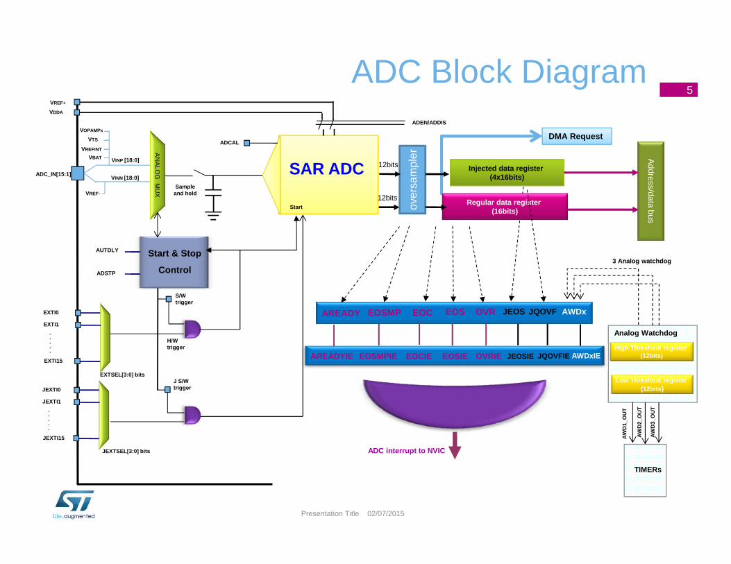
ADC Block Diagram5
02/07/2015Presentation Title
EXTI15
SAR ADC
VREF+
VDDA
EXTSEL[3:0] bits
Address/data bus
DMA Request
Analog Watchdog
High Threshold register(12bits)
Low Threshold register(12bits )
3 Analog watchdog
ADC interrupt to NVIC
EXTI0 AREADY EOSMP OVR JEOSEOS AWDx
12bits
AUTDLY
ADSTP
Start & Stop
Control
Sampleand hold
ADEN/ADDIS
Start
Injected data register(4x16bits)
AN
ALO
G M
UX
ADC_IN[15:1]
VINP [18:0]
VINN [18:0]
VOPAMPx
VTS
VREFINT
VBAT
VREF-
ADCAL
EXTI1
. . . . .
JEXTI15
JEXTI0
JEXTI1
. . . . .
S/W trigger
H/W trigger
J S/W trigger
JEXTSEL[3:0] bits
Regular data register(16bits)
EOC JQOVF
TIMERs
AW
D1_
OU
T
AW
D2_
OU
T
AW
D3_
OU
T
AREADYIE EOSMPIE EOCIE EOSIE OVRIE JEOSIE JQOVFIE AWDxIE
over
sam
pler
12bits
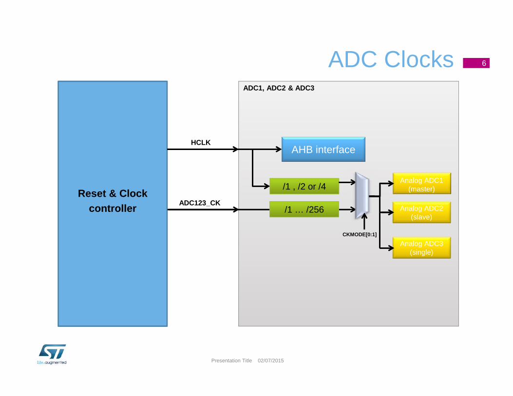
ADC Clocks 6
02/07/2015Presentation Title
Reset & Clock controller
ADC1, ADC2 & ADC3
AHB interfaceHCLK
/1 , /2 or /4
ADC123_CK
Analog ADC1 (master)
Analog ADC2 (slave)
CKMODE[0:1]
/1 … /256
Analog ADC3(single)
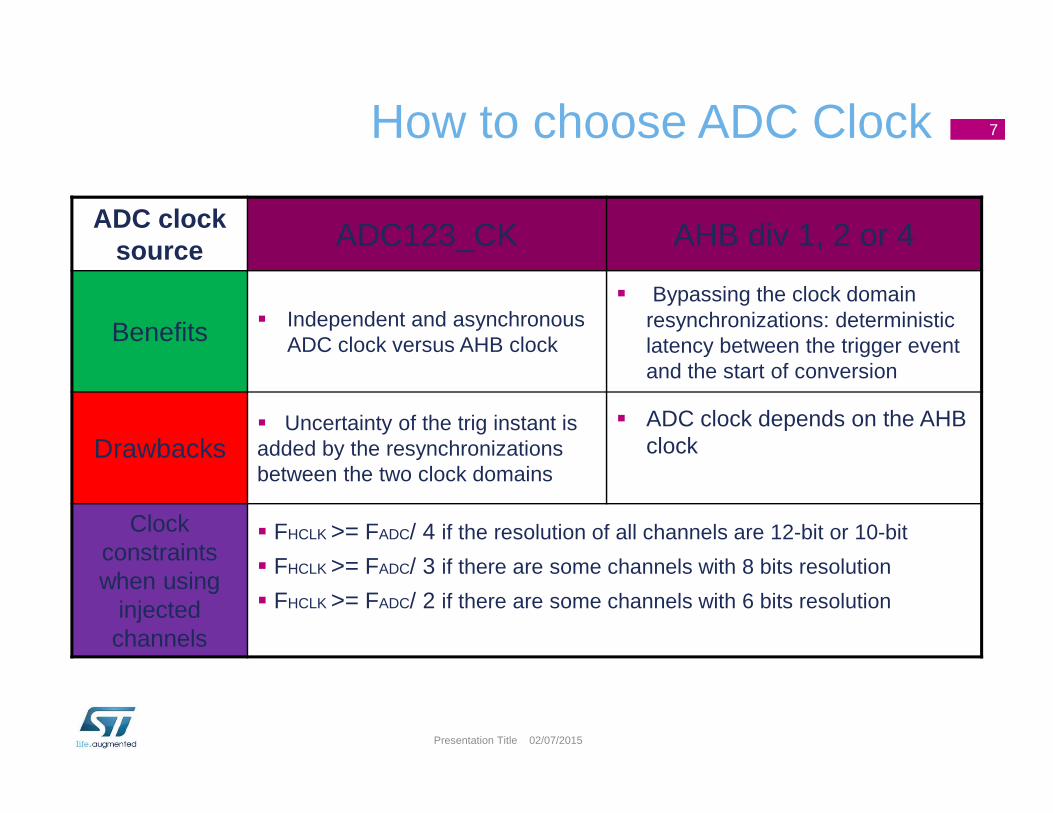
How to choose ADC Clock 7
02/07/2015Presentation Title
ADC clock source ADC123_CK AHB div 1, 2 or 4
Benefits � Independent and asynchronous ADC clock versus AHB clock
� Bypassing the clock domain resynchronizations: deterministic latency between the trigger event and the start of conversion
Drawbacks � Uncertainty of the trig instant is added by the resynchronizations between the two clock domains
� ADC clock depends on the AHB clock
Clock constraints when using
injected channels
� FHCLK >= FADC/ 4 if the resolution of all channels are 12-bit or 10-bit
� FHCLK >= FADC/ 3 if there are some channels with 8 bits resolution
� FHCLK >= FADC/ 2 if there are some channels with 6 bits resolution
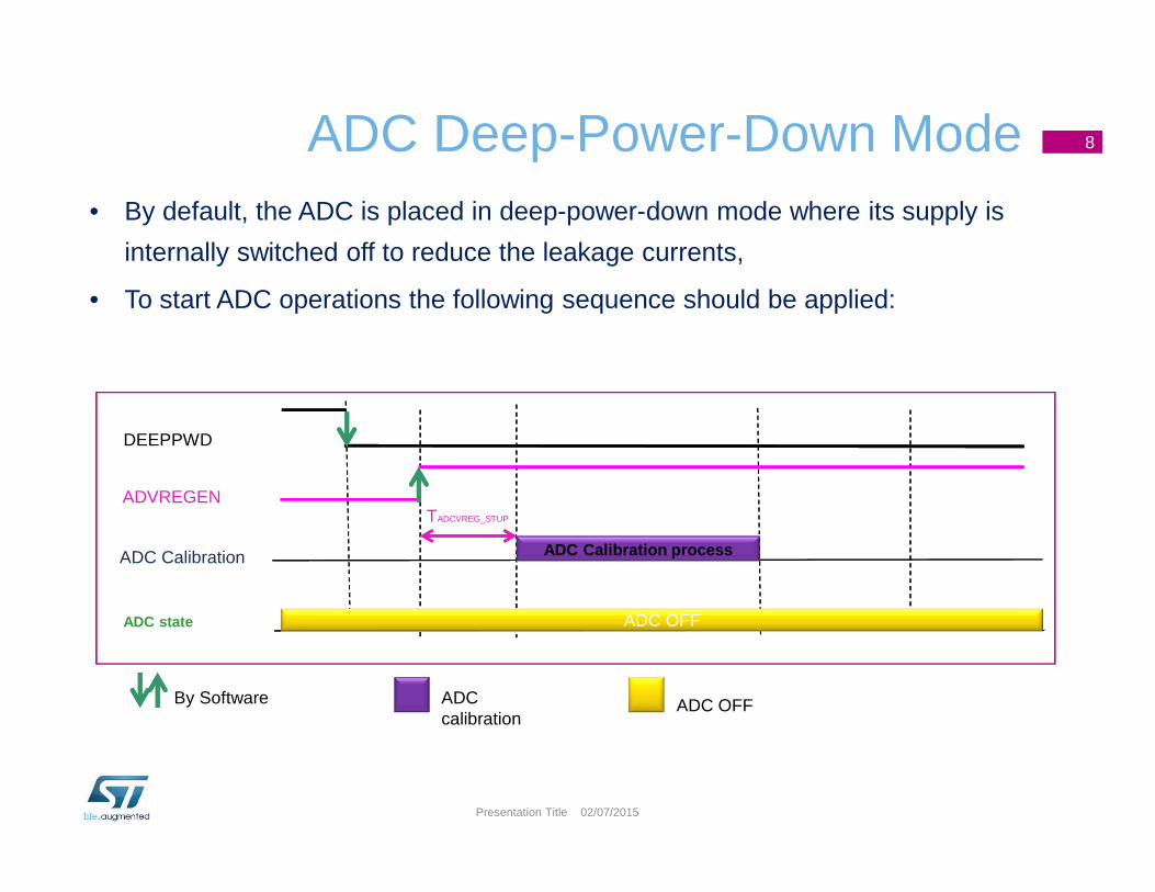
ADC Deep-Power-Down Mode 8
02/07/2015Presentation Title
• By default, the ADC is placed in deep-power-down mode where its supply is
internally switched off to reduce the leakage currents,
• To start ADC operations the following sequence should be applied:
ADC OFFADC calibration
By Software
ADVREGEN
DEEPPWD
ADC state
ADC Calibration ADC Calibration process
ADC OFF
TADCVREG_STUP

ADC Calibration 9
02/07/2015Presentation Title
• The calibration factor to be applied for single-ended input conversions is
different from the factor to be applied for differential input conversions:• If ADCALDIF=0, calibration applied for single conversion and value stored in CALFACT_S
• If ADCALDIF=1, calibration applied for differential conversion and value stored in CALFACT_D
OFF Request
ADCAL
ADCALDIF
ADC Calibration
startup
CALFACT_x[6:0]
ADC state ADC Calibration
ADC StartupBy Software By Hardware
0 : SINGLE ENDED INPUT 1 : DIFFERENTIAL INPUT
OFF OFF
0x00 Calibration factor
Note: The calibration factor is lost when entering Standby, Shutdown, Vbat mode or when the ADC enter deep power down mode. In this case it is possible to re-write the calibration factor into the ADC_CALFACT register without recalibrating.

ADC ON OFF control 10
02/07/2015Presentation Title
• To enable ADC: Set ADEN=1 then wait till ADRDY flag will be equal to 1.
• What ever is the digital and the analog clock of the ADC, ADRDY signal
guarantees that ADC data will be transmitted from one domain to the other.
• ADC cannot be re-programmed unless it is stopped (ADSTART = 0).
OFF Request
OFF
ADRDY
ADEN
ADC ready
OFF startupADC state
T STAB
ADDIS
ADC Ready to convert Req OFF
ADC StartupBy Software By Hardware
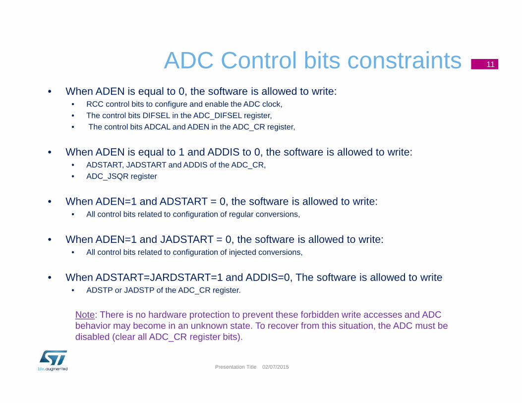
ADC Control bits constraints 11
02/07/2015Presentation Title
• When ADEN is equal to 0, the software is allowed to write:• RCC control bits to configure and enable the ADC clock, • The control bits DIFSEL in the ADC_DIFSEL register,• The control bits ADCAL and ADEN in the ADC_CR register,
• When ADEN is equal to 1 and ADDIS to 0, the software is allowed to write:• ADSTART, JADSTART and ADDIS of the ADC_CR,• ADC_JSQR register
• When ADEN=1 and ADSTART = 0, the software is allowed to write: • All control bits related to configuration of regular conversions,
• When ADEN=1 and JADSTART = 0, the software is allowed to write: • All control bits related to configuration of injected conversions,
• When ADSTART=JARDSTART=1 and ADDIS=0, The software is allowed to write • ADSTP or JADSTP of the ADC_CR register.
Note: There is no hardware protection to prevent these forbidden write accesses and ADC behavior may become in an unknown state. To recover from this situation, the ADC must be disabled (clear all ADC_CR register bits).

ADC Channel selection 12
02/07/2015Presentation Title
• Up to 16 regular and 4 injected conversions with programmable order and programmable sampling time,
Example : - Conversion of channels: 1, 2, 8, 4, 7, 3 and 11
- Different sampling time.
Ch.1 Ch.2 Ch.8 Ch.4 Ch.7 Ch.3 Ch.11
6.5 cycles2.5 cycles
47.5 cycles
2.5 cycles
92.5cycles
24.5cycles
247.5 cycles
ADC Sampling Time (TSampling) 13
02/07/2015Presentation Title
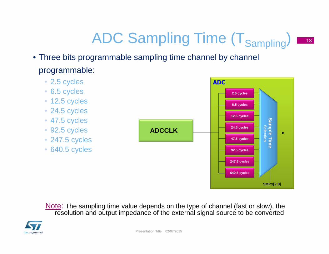
• Three bits programmable sampling time channel by channel
programmable:• 2.5 cycles• 6.5 cycles• 12.5 cycles• 24.5 cycles• 47.5 cycles• 92.5 cycles• 247.5 cycles• 640.5 cycles
ADC
92.5 cycles
6.5 cycles
247.5 cycles
47.5 cycles
12.5 cycles
24.5 cycles
2.5 cycles
640.5 cycles
Sam
pleTim
eS
election
SMPx[2:0]
ADCCLK
Note: The sampling time value depends on the type of channel (fast or slow), the resolution and output impedance of the external signal source to be converted

Total Conversion Time 14
02/07/2015Presentation Title
• Total conversion Time = TSampling + TConversion
Resolution Total conversion Time (When FADC = 80MHz)
12 bits 12.5 + 2.5 = 15cycles 18.75 us � 5.33 Msps
10 bits 10,5 + 2.5 = 13 cycles 16.25 us � 6.15 Msps
8 bits 8.5 + 2.5 = 11 cycles 13.75 us � 7.27 Msps
6 bits 6.5 + 2.5 = 9 cycles 11.25 us � 8.89 Msps
Resolution TConversion
12 bits 12.5 Cycles
10 bits 10.5 Cycles
8 bits 8.5 Cycles
6 bits 6.5 Cycles
End of sampling 15
02/07/2015Presentation Title
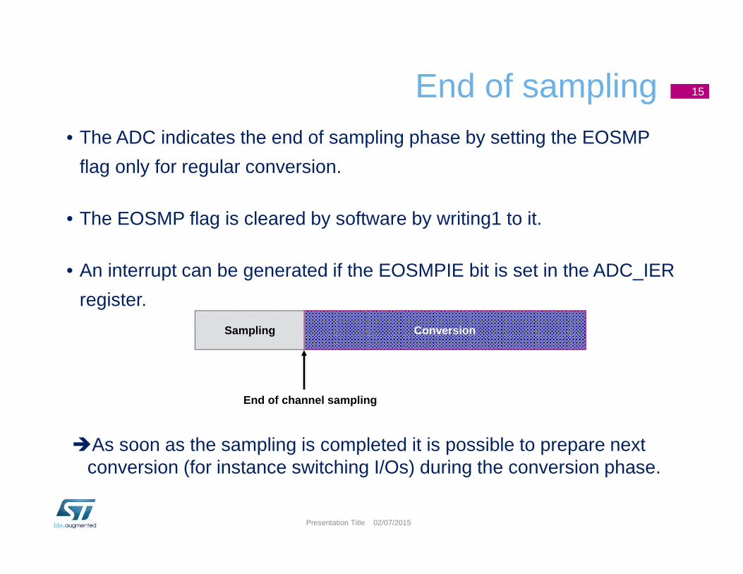
• The ADC indicates the end of sampling phase by setting the EOSMP
flag only for regular conversion.
• The EOSMP flag is cleared by software by writing1 to it.
• An interrupt can be generated if the EOSMPIE bit is set in the ADC_IER
register.
ConversionSampling
End of channel sampling
�As soon as the sampling is completed it is possible to prepare next conversion (for instance switching I/Os) during the conversion phase.

Single-ended & Differential input channels 16
02/07/2015Presentation Title
• Channels can be configured to be either single-ended or differential input by writing ADC_DIFSEL register:
• In single ended input mode, the analog voltage to be converted for channel “i” is the difference between the external voltage ADC_INi (positive input) and VREF-(negative input)
• In differential input mode, the analog voltage to be converted for channel “i” is the difference between the external voltage ADC_INi (positive input) and ADC_INi+1 (negative input)
Note 1: When configuring the channel “i” in differential input mode, channel “i+1” is no longer usable in single-ended mode or in differential mode and must never be configured to be converted.
Analog switches booster
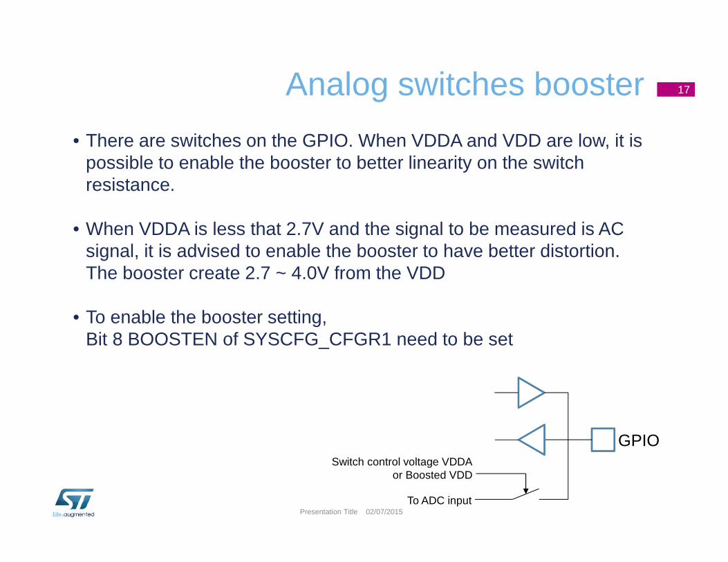
• There are switches on the GPIO. When VDDA and VDD are low, it is possible to enable the booster to better linearity on the switch resistance.
• When VDDA is less that 2.7V and the signal to be measured is AC signal, it is advised to enable the booster to have better distortion. The booster create 2.7 ~ 4.0V from the VDD
• To enable the booster setting, Bit 8 BOOSTEN of SYSCFG_CFGR1 need to be set
17
02/07/2015Presentation TitleTo ADC input
GPIOSwitch control voltage VDDA
or Boosted VDD

IO switch control
• There are two switch series on ADC input. One is in the GPIO and another is ADC input MUXblock. Due to the timing requirement, it is necessary to enable the switch on the GPIO separated from the ADC input mux control.
• The ADC input MUX is selected by the ADC block itself, but the switch in the GPIO need to control bySet the corresponds bit on GPIOx_ASCR register in GPIO block.
18
02/07/2015Presentation Title
GPIOADC input
ADC input MUX
GPIO
ADC conversion modes 19
02/07/2015Presentation Title
CHx
Start
Stop
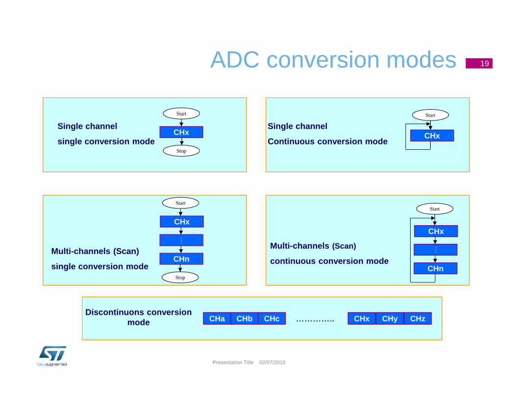
Single channel
single conversion mode
CHx
Start
Stop
...
CHnMulti-channels (Scan)
single conversion mode
CHx
Start
...
CHn
Multi-channels (Scan)
continuous conversion mode
CHx
Start
Single channel
Continuous conversion mode
…………..CHaDiscontinuons conversion
mode CHb CHc CHx CHy CHz

What is the queue of context 20
02/07/2015Presentation Title
• It is a hardware assistant to prepare the context of the injected channels to allow fast context switching
• A queue of context is implemented to anticipate up to 2 contexts for the next injected sequences of conversions,
• The context consist of:• Configuration of the injected triggers (JEXTEN[1:0] and JEXTSEL[3:0]), • Definition of the injected sequence (JSQx[4:0] and JL[1:0]),
• Context parameters are defined in ADC_JSQR register which implements a queue of 2 buffers

How to configure the queue of context 21
02/07/2015Presentation Title
• The JSQR register can be written at any moment even when injected conversions are ongoing.
• At the beginning, the Queue is empty and the first write access into the JSQR register immediately changes the context and the ADC is ready to receive injected triggers.
• Once an injected sequence is complete, the Queue is consumed and the context changes according to the next JSQR parameters stored in the Queue.
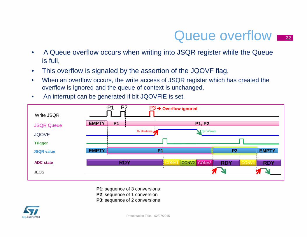
Queue overflow 22
02/07/2015Presentation Title
• A Queue overflow occurs when writing into JSQR register while the Queue is full,
• This overflow is signaled by the assertion of the JQOVF flag,• When an overflow occurs, the write access of JSQR register which has created the
overflow is ignored and the queue of context is unchanged,• An interrupt can be generated if bit JQOVFIE is set.
JSQR Queue
Write JSQR
Trigger
JQOVF
RDY CONV1
By Hardware
P1 P2 P3
EMPTYEMPTY P1P1 P1, P2P1, P2
� Overflow ignored
JSQR value EMPTYEMPTY P1P1
By Software
CONV2 CONV3 RDY
P2P2
CONV1
JEOS
ADC state
EMPTYEMPTY
RDY
P1: sequence of 3 conversionsP2: sequence of 1 conversionP3: sequence of 2 conversions

Queue empty, JQM=0 23
02/07/2015Presentation Title
• When the Queue become empty:• If JQM=0 � The Queue is maintained with the last active context,
JSQR Queue
Write JSQR
Trigger
RDY CONV1
P1 P2
EMPTYEMPTY P1P1 P1, P2P1, P2
JSQR value EMPTYEMPTY
CONV1 RDY
P2P2
ADC state
sequence of 1 conversion
sequence of 1 conversion
RDY
P1P1
P2P2
RDY CONV1
The Queue is not empty and maintains P2 because JQM=0
P1
P2
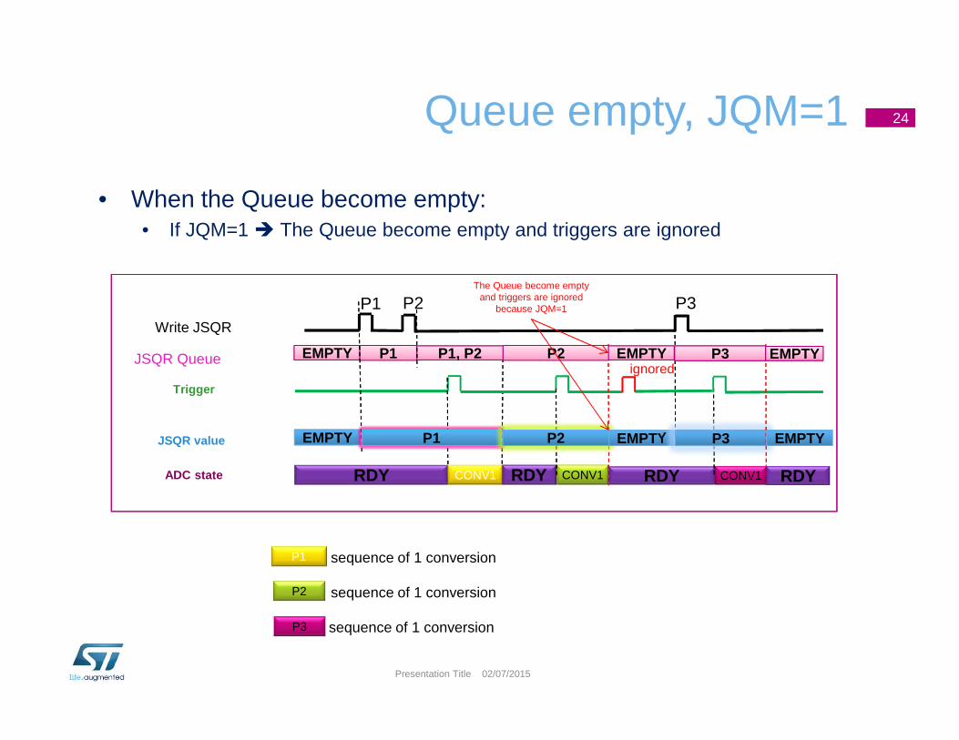
Queue empty, JQM=1 24
02/07/2015Presentation Title
• When the Queue become empty:• If JQM=1 � The Queue become empty and triggers are ignored
JSQR Queue
Write JSQR
Trigger
RDY CONV1
P1 P2
EMPTYEMPTY P1P1 P1, P2P1, P2
JSQR value EMPTYEMPTY
CONV1ADC state
sequence of 1 conversion
sequence of 1 conversion
sequence of 1 conversion
RDY
P1P1
P2P2
RDY CONV1
The Queue become emptyand triggers are ignored
because JQM=1
P1
P2
EMPTYEMPTY
P2P2
P3
P3P3
EMPTYEMPTY P3P3
EMPTYEMPTY
EMPTYEMPTY
RDY
ignored
P3

ADC Channel offset 25
02/07/2015Presentation Title
• An offset x (x=1,2,3,4) can be applied to a channel by setting the OFFSETx_EN of ADC_OFRx register.
• The channel to which the offset will be applied is programmed into the bits OFFSETx_CH of ADC_OFRx register.
• In this case, the converted value is decreased by the user-defined offset written in the OFFSETx bits.
• The result may be a negative value so the read data is signed and the SEXT bit represents the extended sign value.
Right alignment
0 0 0D11 D10 D9 D8 D7 D6 D5 D4 D3 D2 D1 D0
Left alignment
0 0 0D11 D10 D9 D8 D7 D6 D5 D4 D3 D2 D1 D0
Offset disabled, unsigned value
SEXT SEXT SEXT SEXT D11 D10 D9 D8 D7 D6 D5 D4 D3 D2 D1 D0
0 0 0 0 D11 D10 D9 D8 D7 D6 D5 D4 D3 D2 D1 D0
Offset enabled, signed value
Offset disabled, unsigned value
Offset enabled, signed value
0
SEXT
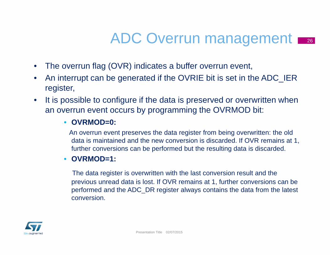
ADC Overrun management 26
02/07/2015Presentation Title
• The overrun flag (OVR) indicates a buffer overrun event,• An interrupt can be generated if the OVRIE bit is set in the ADC_IER
register,• It is possible to configure if the data is preserved or overwritten when
an overrun event occurs by programming the OVRMOD bit:• OVRMOD=0:
An overrun event preserves the data register from being overwritten: the old data is maintained and the new conversion is discarded. If OVR remains at 1, further conversions can be performed but the resulting data is discarded.
• OVRMOD=1:
The data register is overwritten with the last conversion result and the previous unread data is lost. If OVR remains at 1, further conversions can be performed and the ADC_DR register always contains the data from the latest conversion.
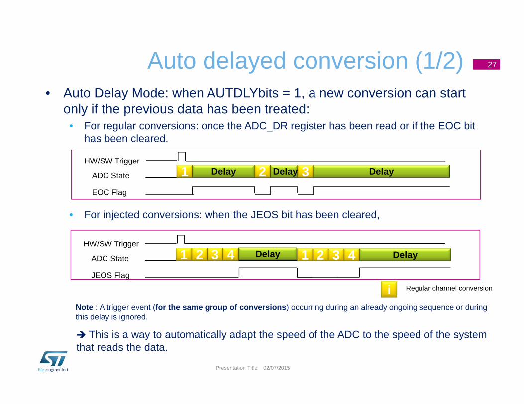
Auto delayed conversion (1/2) 27
02/07/2015Presentation Title
• Auto Delay Mode: when AUTDLYbits = 1, a new conversion can start only if the previous data has been treated:
• For regular conversions: once the ADC_DR register has been read or if the EOC bit has been cleared.
• For injected conversions: when the JEOS bit has been cleared,
i Regular channel conversion
� This is a way to automatically adapt the speed of the ADC to the speed of the system that reads the data.
Note : A trigger event (for the same group of conversions ) occurring during an already ongoing sequence or during this delay is ignored.
3 DelayDelay2Delay1ADC State
HW/SW Trigger
EOC Flag
3 Delay21ADC State
HW/SW Trigger
JEOS Flag
4 321 4 Delay

Auto delayed conversion (2/2) 28
02/07/2015Presentation Title
• No delay inserted between each conversions of different groups (a regular conversion followed by an injected conversion or conversely)
• If an injected trigger occur during the automatic delay of a regular conversion, the injected conversion starts immediately.
• Once the injected sequence is complete, ADC waits the delay of the previous regular conversion before lunching new regular conversion.
• In auto-injected mode (JAUTO=1) a new regular conversion can start only when the automatic delay of the previous injected sequence of conversion has ended (when JEOS has been cleared),

ADC Analog Watchdogs 29
02/07/2015Presentation Title
• ADC Analog Watchdog 1
• 12-bit programmable analog watchdog low and high thresholds
• Enabled on one or all converted channels
• Interrupt generation on low or high thresholds detection
• ADC Analog Watchdog 2&3
• Enabled on some selected channels by programming bits in AWDCHx[18:0],
• Resolution Limited to 8 bits and only the 8 MSBs of the thresholds can be programmed
into HTx[7:0] and LTx[7:0]
Status RegisterAnalog Watchdog
Low Threshold
ADC_IN0
ADC_IN1
ADC_IN18
AWD
High Threshold...
.
.
.
Note : The watchdog comparison is performed on the raw converted data before any alignment calculation and before applying any offsets.
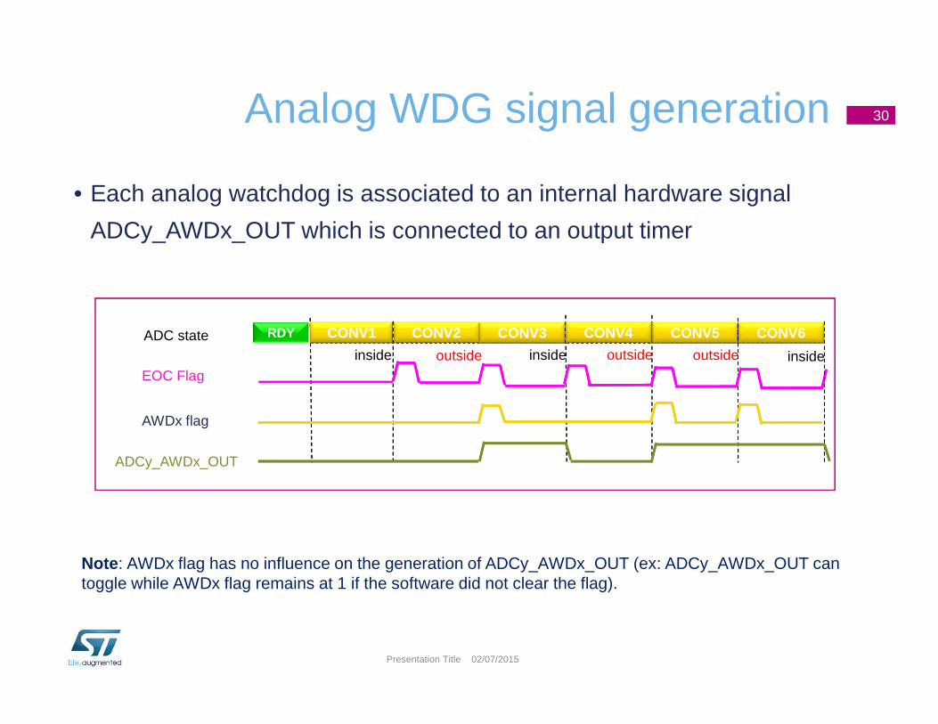
Analog WDG signal generation 30
02/07/2015Presentation Title
• Each analog watchdog is associated to an internal hardware signal
ADCy_AWDx_OUT which is connected to an output timer
Note: AWDx flag has no influence on the generation of ADCy_AWDx_OUT (ex: ADCy_AWDx_OUT can toggle while AWDx flag remains at 1 if the software did not clear the flag).
EOC Flag
ADC state RDY
AWDx flag
CONV1 CONV2 CONV3 CONV4 CONV5 CONV6
inside outside inside outside outside inside
ADCy_AWDx_OUT

DMACFG bit management 31
02/07/2015Presentation Title
• DMA can be used to manage the regular channels conversions (ADCx
DR register),
• DMA one shot mode (DMACFG = 0):
In this mode the ADC stops generating DMA requests once the DMA has reached the
last DMA transfer even if conversion has been started again.
• DMA circular mode (DMACFG=1):
In this mode, the ADC generates a DMA transfer request each time a new conversion
data is available in the data register, even if the DMA has reached the last DMA
transfer.
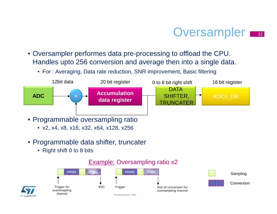
Oversampler
• Oversampler performes data pre-processing to offload the CPU. Handles upto 256 conversion and average then into a single data.
• For : Averaging, Data rate reduction, SNR improvement, Basic filtering
• Programmable oversampling ratio• x2, x4, x8, x16, x32, x64, x128, x256
• Programmable data shifter, truncater• Right shift 0 to 8 bits
32
Presentation Title
ADC + Accumulationdata register
12bit data
DATASHIFTER,
TRUNCATER
20 bit register
ADCx_DR
16 bit register0 to 8 bit right shift
CH1(0) CH1(1) CH1(0) CH1(1)
Trigger for oversmapling
channel
Sampling
ConversionEOC Trigger End of conversion for
oversampling channel
Example: Oversampling ratio x2

ADC Dual mode 33
02/07/2015Presentation Title
• ADC1 and ADC2 can be used together in Dual mode (ADC1 is the master),
• Seven possible modes are implemented:
• Injected simultaneous mode,
• Regular simultaneous mode,
• Interleaved mode,
• Alternate trigger mode
• Injected simultaneous + Regular simultaneous mode,
• Regular simultaneous + Injected Alternate trigger mode,
• Injected simultaneous + Interleave mode,
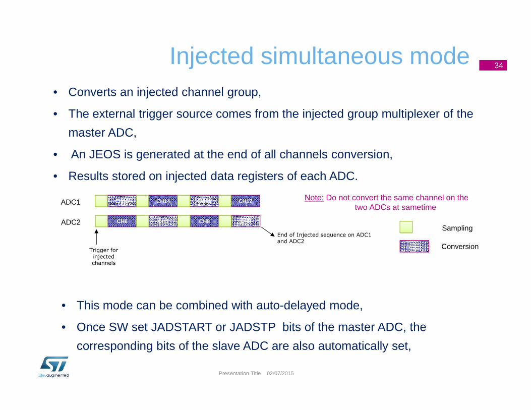
Injected simultaneous mode 34
02/07/2015Presentation Title
• Converts an injected channel group,
• The external trigger source comes from the injected group multiplexer of the
master ADC,
• An JEOS is generated at the end of all channels conversion,
• Results stored on injected data registers of each ADC.
Note: Do not convert the same channel on the two ADCs at sametime
CH15 CH14 CH13 CH12ADC1
SamplingCH6 CH7 CH8 CH9ADC2
Trigger for injected channels
End of Injected sequence on ADC1 and ADC2
Conversion
• This mode can be combined with auto-delayed mode,
• Once SW set JADSTART or JADSTP bits of the master ADC, the
corresponding bits of the slave ADC are also automatically set,
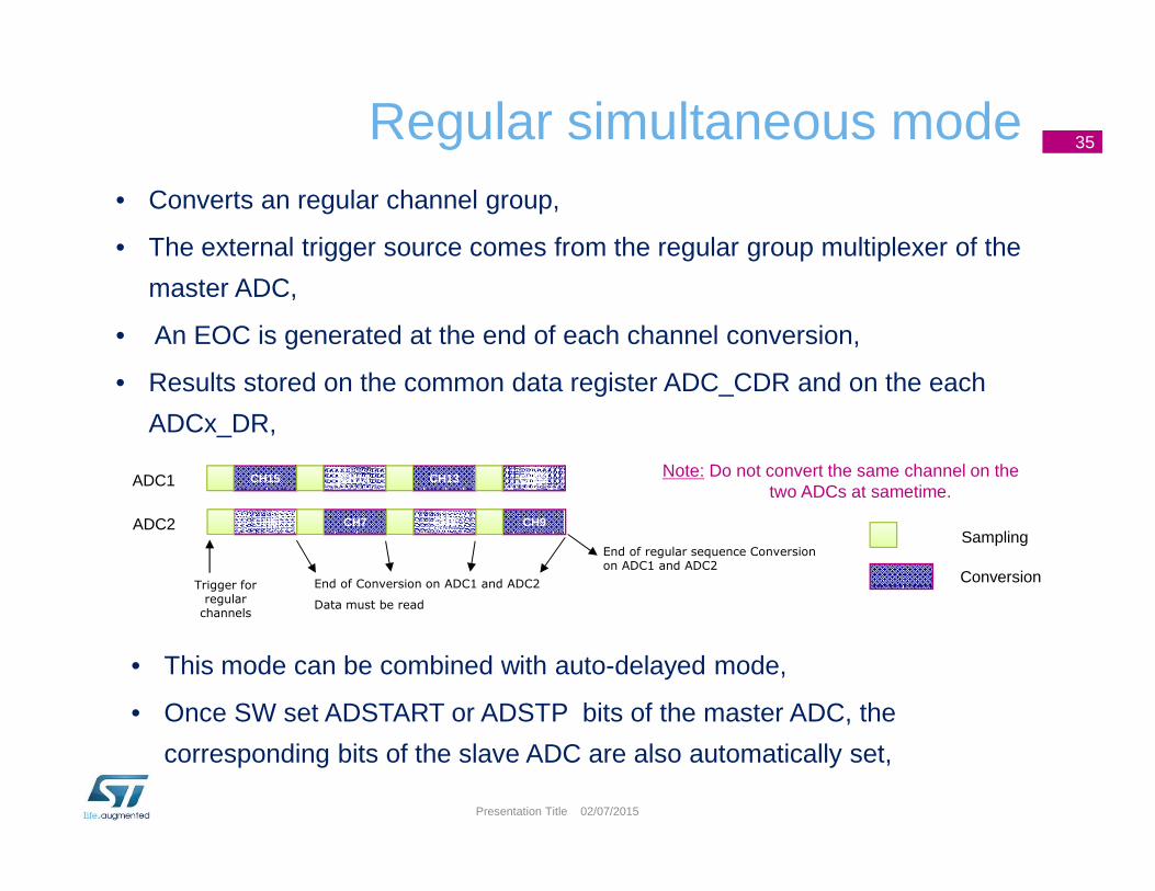
Regular simultaneous mode 35
02/07/2015Presentation Title
• Converts an regular channel group,
• The external trigger source comes from the regular group multiplexer of the
master ADC,
• An EOC is generated at the end of each channel conversion,
• Results stored on the common data register ADC_CDR and on the each
ADCx_DR,
Note: Do not convert the same channel on the two ADCs at sametime.
CH15 CH14 CH13 CH12ADC1
SamplingCH6 CH7 CH8 CH9ADC2
Trigger for regular
channels
End of regular sequence Conversion on ADC1 and ADC2
Conversion
• This mode can be combined with auto-delayed mode,
• Once SW set ADSTART or ADSTP bits of the master ADC, the
corresponding bits of the slave ADC are also automatically set,
End of Conversion on ADC1 and ADC2
Data must be read
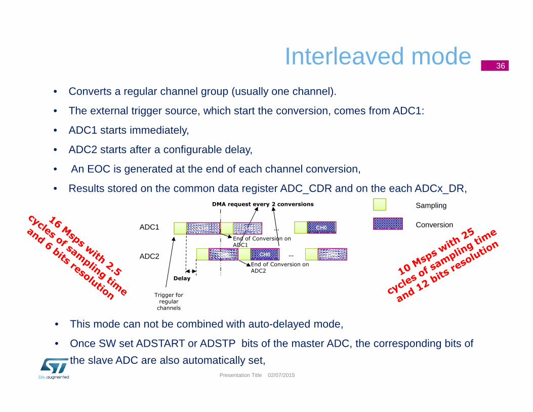
Interleaved mode 36
02/07/2015Presentation Title
• Converts a regular channel group (usually one channel).
• The external trigger source, which start the conversion, comes from ADC1:
• ADC1 starts immediately,
• ADC2 starts after a configurable delay,
• An EOC is generated at the end of each channel conversion,
• Results stored on the common data register ADC_CDR and on the each ADCx_DR,
• This mode can not be combined with auto-delayed mode,
• Once SW set ADSTART or ADSTP bits of the master ADC, the corresponding bits of
the slave ADC are also automatically set,
CH0ADC1
ADC2
Sampling
Conversion
Trigger for regular
channels
Delay
…
… CH0
CH0CH0
CH0
DMA request every 2 conversions
CH0
End of Conversion on ADC2
End of Conversion on ADC1

Alternate trigger mode 37
02/07/2015Presentation Title
• Converts an injected channel group,
• The external trigger source comes from the injected group multiplexer of the master
ADC,
• If discontinuous mode is enabled:
• This mode can not be combined with auto-delayed mode,
• Once SW set JADSTART or JADSTP bits of the master ADC, the corresponding bits
of the slave ADC are also automatically set,
CH0ADC1
ADC2
Sampling
CH11
CH1
CH12 CH13
CH2 CH3
1st
Trigger3rd
Trigger5th
Trigger
7th
Trigger
CH10
JEOC, JEOS on ADC1JEOC JEOC JEOC
JEOC JEOC JEOC JEOC, JEOS on ADC22nd
Trigger
4th
Trigger6th
Trigger
8th
Trigger
Conversion• If discontinuous mode is disabled:
CH15 CH14ADC1
CH6 CH7ADC2
1st
Trigger
CH12
CH8
2nd
Trigger
CH15 CH14
CH6 CH7
3td
Trigger
CH12
CH8
4th
Trigger
JEOC JEOC JEOC, JEOS JEOC JEOC
JEOCJEOCJEOCJEOC JEOC, JEOS JEOC, JEOS
JEOC, JEOS

Regular simultaneous + Injected simultaneous
38
02/07/2015Presentation Title
• Converts an injected and regular channel groups,
• The external trigger source comes from the master ADC,
• Results of injected channels stored on ADCx_JDRy registers, and regular channels on
each ADCx_DR register and on ADC_CDR register.
CH0 CH1 CH1 CH2
CH3 CH2 CH2 CH1
ADC1
ADC2
Trigger for regular
channels
End of Seaquence on on ADC1 and ADC2
CH10 CH11
CH15 CH14
ADC1
ADC2
Trigger for injectedchannels
End of Injected Conversion(JEOS) on ADC1 and ADC2
regular simultaneous
mode interrupted by
injected simultaneous
one
CH3
CH0
Note: Do not convert the same channel on the two ADCs at same time
Sampling
Conversion
• This mode can be combined with auto-delayed mode,
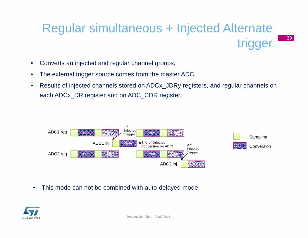
Regular simultaneous + Injected Alternate trigger
39
02/07/2015Presentation Title
• Converts an injected and regular channel groups,
• The external trigger source comes from the master ADC,
• Results of injected channels stored on ADCx_JDRy registers, and regular channels on
each ADCx_DR register and on ADC_CDR register.
• This mode can not be combined with auto-delayed mode,
CH0 CH1 CH1 CH2
CH3 CH0 CH0 CH1
ADC1 reg
ADC2 reg
ADC1 inj
ADC2 inj
CH10 2nd
injected Trigger
CH11
End of Injected Conversion on ADC1
1st
injected Trigger
Sampling
Conversion
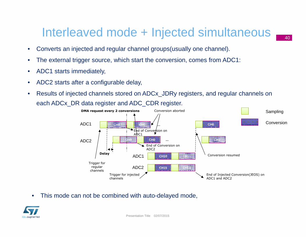
Interleaved mode + Injected simultaneous40
02/07/2015Presentation Title
• Converts an injected and regular channel groups(usually one channel).
• The external trigger source, which start the conversion, comes from ADC1:
• ADC1 starts immediately,
• ADC2 starts after a configurable delay,
• Results of injected channels stored on ADCx_JDRy registers, and regular channels on
each ADCx_DR data register and ADC_CDR register.
• This mode can not be combined with auto-delayed mode,
CH0ADC1
ADC2
Sampling
Conversion
Trigger for regular
channels
Delay
…
… CH0
CH0CH0
CH0
DMA request every 2 conversions
CH0
End of Conversion on ADC2
End of Conversion on ADC1
CH10 CH11
CH15 CH14
ADC1
ADC2
Trigger for injectedchannels
End of Injected Conversion(JEOS) on ADC1 and ADC2
Conversion aborted
Conversion resumed

DMA requests in dual ADC mode 41
02/07/2015Presentation Title
• MDMA=0b00:• One DMA channel should be configured for each ADC to transfer the data available on
ADCx_DR register,
• MDMA=0b10:• A single DMA request is generated each time both master and slave EOC events have
occurred,
• Used in interleaved and in regular simultaneous mode when ADC resolution is 10 or 12 bitsDMA request ADC_CDR[31:0] = SLV_ADC_DR[15:0] | MST_ADC_DR[15:0]
• MDMA=0b11:• A single DMA request is generated each time both master and slave EOC events have
occurred,
• Used in interleaved and in regular simultaneous mode when ADC resolution is 6 or 8 bitsDMA request ADC_CDR[15:0] = SLV_ADC_DR[7:0] | MST_ADC_DR[7:0]

ADC Flags and interrupts 42
02/07/2015Presentation Title
Interrupt enable bits
ADC
Global interrupt
(NVIC)
EOSMP
ADRDY
OVR
EOC
EOS
AWD1
Flags
ADRDY: « ADC ready »
EOC : « Regular E nd Of Conversion »
EOS : « Regular End Of Sequence »
AWD1 : « Analog watchdog 1»
OVRIE
EOCIE
EOSIE
AWD1IE
ADRDYIE
EOSMPIE
JEOC : « Injected E nd Of Conversion » JEOC JEOCIE
JEOS : « Injected End Of Sequence »JEOS JEOSIE
AWD2 : « Analog watchdog 2»
AWD3 : « Analog watchdog 3»
AWD2IEAWD2
AWD3IEAWD3
EOSMP: End Of Sampling
OVR: Overrun
JQOVF : «Injected Injected context queue overflows» JQOVF JQOVFIE
Temperature sensor and bandgap 43
02/07/2015Presentation Title
• Internal voltage reference Vrefint (bandgap) has 2 modes:• Normal mode in Run mode
• Low-power mode in all other modes including Low-power run mode• Note: Bandgap is OFF in Shutdown mode.
• When exiting Stop 1, Stop 2, Standby or Low-power run, the bandgapcannot be used during a time around TSTART 120 µs max
• Temperature sensor needs bandgap to be in Normal mode. The TSTART
temporization must be wait before converting temperature sensor• After the transition from Stop 1, Stop 2, Standby to Run mode
• In Low-power run mode, after enabling the temperature sensor• This switches the bandgap in Normal mode
• After the transition from Low-power run mode to Run mode