Embed Size (px)
Citation preview

March 2021 UM2324 Rev 4 1/43
1
UM2324User manual
STM32 Nucleo-64 boards (MB1360)
Introduction
The STM32 Nucleo-64 boards, based on the MB1360 reference board (NUCLEO-G070RB, NUCLEO-G071RB, and NUCLEO-G0B1RE order codes) provide an affordable and flexible way for users to try out new concepts and build prototypes with the STM32 microcontroller, which provide various combinations of performance, power consumption, and features.ARDUINO® Uno V3 connectivity and ST morpho headers provide easy means of expanding the functionality of the Nucleo open development platform with a wide choice of specialized shields.The STM32 Nucleo-64 boards do not require any separate probe, as they integrate the ST-LINK/V2-1 debugger/programmer. The STM32 Nucleo-64 boards come with the comprehensive free STM32 software libraries and examples that are available with the STM32CubeG0 MCU Package.
Figure 1. STM32 Nucleo-64 board top view
Picture is not contractual.
www.st.com

Contents UM2324
2/43 UM2324 Rev 4
Contents
1 Features . . . . . . . . . . . . . . . . . . . . . . . . . . . . . . . . . . . . . . . . . . . . . . . . . . . 7
2 Ordering information . . . . . . . . . . . . . . . . . . . . . . . . . . . . . . . . . . . . . . . . 8
2.1 Codification . . . . . . . . . . . . . . . . . . . . . . . . . . . . . . . . . . . . . . . . . . . . . . . . . 8
3 Development environment . . . . . . . . . . . . . . . . . . . . . . . . . . . . . . . . . . . . 9
3.1 System requirements . . . . . . . . . . . . . . . . . . . . . . . . . . . . . . . . . . . . . . . . . 9
3.2 Development toolchains . . . . . . . . . . . . . . . . . . . . . . . . . . . . . . . . . . . . . . . 9
3.3 Demonstration software . . . . . . . . . . . . . . . . . . . . . . . . . . . . . . . . . . . . . . . 9
4 Conventions . . . . . . . . . . . . . . . . . . . . . . . . . . . . . . . . . . . . . . . . . . . . . . . . 9
5 Quick start . . . . . . . . . . . . . . . . . . . . . . . . . . . . . . . . . . . . . . . . . . . . . . . . 10
5.1 Getting started . . . . . . . . . . . . . . . . . . . . . . . . . . . . . . . . . . . . . . . . . . . . . 10
6 Hardware layout and configuration . . . . . . . . . . . . . . . . . . . . . . . . . . . . 11
6.1 STM32 Nucleo-64 board mechanical drawing . . . . . . . . . . . . . . . . . . . . . 13
6.2 Default board configuration . . . . . . . . . . . . . . . . . . . . . . . . . . . . . . . . . . . 13
6.3 Cuttable PCB . . . . . . . . . . . . . . . . . . . . . . . . . . . . . . . . . . . . . . . . . . . . . . 13
6.4 Embedded ST-LINK/V2-1 . . . . . . . . . . . . . . . . . . . . . . . . . . . . . . . . . . . . . 14
6.4.1 Drivers . . . . . . . . . . . . . . . . . . . . . . . . . . . . . . . . . . . . . . . . . . . . . . . . . . 15
6.4.2 ST-LINK/V2-1 firmware upgrade . . . . . . . . . . . . . . . . . . . . . . . . . . . . . . 15
6.4.3 Using the ST-LINK/V2-1 to program/debug the STM32 on board . . . . . 15
6.4.4 Using ST-LINK/V2-1 to program/debug an external STM32 application 16
6.5 Power supply and power selection . . . . . . . . . . . . . . . . . . . . . . . . . . . . . . 17
6.5.1 External power supply input . . . . . . . . . . . . . . . . . . . . . . . . . . . . . . . . . . 17
6.5.2 External power supply output: . . . . . . . . . . . . . . . . . . . . . . . . . . . . . . . . 22
6.6 Programming/debugging when the power supply is not from ST-LINK . . 22
6.7 OSC clock sources . . . . . . . . . . . . . . . . . . . . . . . . . . . . . . . . . . . . . . . . . . 23
6.7.1 LSE: OSC 32 kHz clock supply . . . . . . . . . . . . . . . . . . . . . . . . . . . . . . . 23
6.7.2 HSE: OSC 8 MHz clock supply . . . . . . . . . . . . . . . . . . . . . . . . . . . . . . . 24
6.8 Reset sources . . . . . . . . . . . . . . . . . . . . . . . . . . . . . . . . . . . . . . . . . . . . . 24
6.9 UART2 communication . . . . . . . . . . . . . . . . . . . . . . . . . . . . . . . . . . . . . . 24
UM2324 Rev 4 3/43
UM2324 Contents
4
6.10 LEDs . . . . . . . . . . . . . . . . . . . . . . . . . . . . . . . . . . . . . . . . . . . . . . . . . . . . 25
6.11 Push-buttons . . . . . . . . . . . . . . . . . . . . . . . . . . . . . . . . . . . . . . . . . . . . . . 25
6.12 IDD measurement . . . . . . . . . . . . . . . . . . . . . . . . . . . . . . . . . . . . . . . . . . . 26
6.13 Jumper configuration . . . . . . . . . . . . . . . . . . . . . . . . . . . . . . . . . . . . . . . . 26
6.14 Configuration of the solder bridges . . . . . . . . . . . . . . . . . . . . . . . . . . . . . 26
7 Connectors . . . . . . . . . . . . . . . . . . . . . . . . . . . . . . . . . . . . . . . . . . . . . . . 28
7.1 CN2 USB Micro-B connector . . . . . . . . . . . . . . . . . . . . . . . . . . . . . . . . . . 28
7.2 ARDUINO® Uno V3 connector . . . . . . . . . . . . . . . . . . . . . . . . . . . . . . . . . 29
7.3 CN7 and CN10 ST morpho connectors . . . . . . . . . . . . . . . . . . . . . . . . . . 32
8 STM32 Nucleo-64 board information . . . . . . . . . . . . . . . . . . . . . . . . . . . 34
8.1 Product marking . . . . . . . . . . . . . . . . . . . . . . . . . . . . . . . . . . . . . . . . . . . . 34
8.2 NUCLEO-G070RB product history . . . . . . . . . . . . . . . . . . . . . . . . . . . . . . 34
8.2.1 Product identification NUG070RB$AU1 . . . . . . . . . . . . . . . . . . . . . . . . 34
8.2.2 Product identification NUG070RB$AU2 . . . . . . . . . . . . . . . . . . . . . . . . 34
8.3 NUCLEO-G071RB product history . . . . . . . . . . . . . . . . . . . . . . . . . . . . . . 35
8.3.1 Product identification NUG071RB$AU1 . . . . . . . . . . . . . . . . . . . . . . . . 35
8.3.2 Product identification NUG071RB$AU2 . . . . . . . . . . . . . . . . . . . . . . . . 35
8.4 NUCLEO-G0B1RE product history . . . . . . . . . . . . . . . . . . . . . . . . . . . . . 35
8.4.1 Product identification NUG0B1RE$AU1 . . . . . . . . . . . . . . . . . . . . . . . . 35
8.5 Board revision history . . . . . . . . . . . . . . . . . . . . . . . . . . . . . . . . . . . . . . . . 36
8.5.1 Board MB1360 revision C-01 . . . . . . . . . . . . . . . . . . . . . . . . . . . . . . . . . 36
8.5.2 Board MB1360 revision C-02 . . . . . . . . . . . . . . . . . . . . . . . . . . . . . . . . . 36
Appendix A STM32 Nucleo-64 board I/O assignment . . . . . . . . . . . . . . . . . . . . . 37
Appendix B Federal Communications Commission (FCC) and ISED Canada Compliance Statements. . . . . . . . . . . . . . . . . . . . . . . 39
B.1 FCC Compliance Statement . . . . . . . . . . . . . . . . . . . . . . . . . . . . . . . . . . . 39
B.2 ISED Compliance Statement. . . . . . . . . . . . . . . . . . . . . . . . . . . . . . . . . . . 40
Appendix C CE conformity . . . . . . . . . . . . . . . . . . . . . . . . . . . . . . . . . . . . . . . . . . 41
C.1 Warning . . . . . . . . . . . . . . . . . . . . . . . . . . . . . . . . . . . . . . . . . . . . . . . . . . . 41
C.2 Simplified declaration of conformity. . . . . . . . . . . . . . . . . . . . . . . . . . . . . . 41

Contents UM2324
4/43 UM2324 Rev 4
Revision history . . . . . . . . . . . . . . . . . . . . . . . . . . . . . . . . . . . . . . . . . . . . . . . . . . . . 42
UM2324 Rev 4 5/43
UM2324 List of tables
5
List of tables
Table 1. Ordering information . . . . . . . . . . . . . . . . . . . . . . . . . . . . . . . . . . . . . . . . . . . . . . . . . . . . . . . 8Table 2. Codification explanation . . . . . . . . . . . . . . . . . . . . . . . . . . . . . . . . . . . . . . . . . . . . . . . . . . . . 8Table 3. ON/OFF conventions . . . . . . . . . . . . . . . . . . . . . . . . . . . . . . . . . . . . . . . . . . . . . . . . . . . . . . 9Table 4. Default jump settings . . . . . . . . . . . . . . . . . . . . . . . . . . . . . . . . . . . . . . . . . . . . . . . . . . . . . 13Table 5. ST-LINK jumper configuration . . . . . . . . . . . . . . . . . . . . . . . . . . . . . . . . . . . . . . . . . . . . . . 14Table 6. CN11 debug connector (SWD) . . . . . . . . . . . . . . . . . . . . . . . . . . . . . . . . . . . . . . . . . . . . . . 16Table 7. Power supply capabilities . . . . . . . . . . . . . . . . . . . . . . . . . . . . . . . . . . . . . . . . . . . . . . . . . . 18Table 8. UART2 pins . . . . . . . . . . . . . . . . . . . . . . . . . . . . . . . . . . . . . . . . . . . . . . . . . . . . . . . . . . . . 25Table 9. Jumper configuration . . . . . . . . . . . . . . . . . . . . . . . . . . . . . . . . . . . . . . . . . . . . . . . . . . . . . 26Table 10. Solder bridge configurations and settings. . . . . . . . . . . . . . . . . . . . . . . . . . . . . . . . . . . . . . 26Table 11. USB Micro-B pinout . . . . . . . . . . . . . . . . . . . . . . . . . . . . . . . . . . . . . . . . . . . . . . . . . . . . . . 28Table 12. ARDUINO® connector pinout . . . . . . . . . . . . . . . . . . . . . . . . . . . . . . . . . . . . . . . . . . . . . . . 30Table 13. STM32 Nucleo-64 board I/O assignment . . . . . . . . . . . . . . . . . . . . . . . . . . . . . . . . . . . . . . 37Table 14. Document revision history . . . . . . . . . . . . . . . . . . . . . . . . . . . . . . . . . . . . . . . . . . . . . . . . . 42

List of figures UM2324
6/43 UM2324 Rev 4
List of figures
Figure 1. STM32 Nucleo-64 board top view . . . . . . . . . . . . . . . . . . . . . . . . . . . . . . . . . . . . . . . . . . . . 1Figure 2. Hardware block diagram. . . . . . . . . . . . . . . . . . . . . . . . . . . . . . . . . . . . . . . . . . . . . . . . . . . 11Figure 3. Top layout . . . . . . . . . . . . . . . . . . . . . . . . . . . . . . . . . . . . . . . . . . . . . . . . . . . . . . . . . . . . . . 12Figure 4. Bottom layout . . . . . . . . . . . . . . . . . . . . . . . . . . . . . . . . . . . . . . . . . . . . . . . . . . . . . . . . . . . 12Figure 5. STM32 Nucleo-64 board mechanical drawing . . . . . . . . . . . . . . . . . . . . . . . . . . . . . . . . . . 13Figure 6. USB composite device . . . . . . . . . . . . . . . . . . . . . . . . . . . . . . . . . . . . . . . . . . . . . . . . . . . . 15Figure 7. STM32 Nucleo-64 board connections image . . . . . . . . . . . . . . . . . . . . . . . . . . . . . . . . . . . 16Figure 8. ST-LINK connections image . . . . . . . . . . . . . . . . . . . . . . . . . . . . . . . . . . . . . . . . . . . . . . . . 17Figure 9. STLK power source . . . . . . . . . . . . . . . . . . . . . . . . . . . . . . . . . . . . . . . . . . . . . . . . . . . . . . 19Figure 10. JP2 [3-4]: STLK power source . . . . . . . . . . . . . . . . . . . . . . . . . . . . . . . . . . . . . . . . . . . . . . 20Figure 11. JP2 [5-6]: STLK power source . . . . . . . . . . . . . . . . . . . . . . . . . . . . . . . . . . . . . . . . . . . . . . 21Figure 12. JP2 [7-8]: CHG power source. . . . . . . . . . . . . . . . . . . . . . . . . . . . . . . . . . . . . . . . . . . . . . . 22Figure 13. CN2 USB Micro-B connector (front view) . . . . . . . . . . . . . . . . . . . . . . . . . . . . . . . . . . . . . . 28Figure 14. ARDUINO® connectors. . . . . . . . . . . . . . . . . . . . . . . . . . . . . . . . . . . . . . . . . . . . . . . . . . . . 29Figure 15. STM32 Nucleo-64 boards ARDUINO® connector pinout . . . . . . . . . . . . . . . . . . . . . . . . . . 30Figure 16. ST morpho connectors . . . . . . . . . . . . . . . . . . . . . . . . . . . . . . . . . . . . . . . . . . . . . . . . . . . . 32Figure 17. STM32 Nucleo-64 boards ST morpho connector pinout . . . . . . . . . . . . . . . . . . . . . . . . . . 33

UM2324 Rev 4 7/43
UM2324 Features
42
1 Features
• STM32 Arm®(a)-based microcontroller in LQFP64 package
• 1 user LED shared with ARDUINO®
• 1 user and 1 reset push-buttons
• 32.768 kHz crystal oscillator
• Board connectors:
– ARDUINO® Uno V3 expansion connector
– ST morpho extension pin headers for full access to all STM32 I/Os
• Flexible power-supply options: ST-LINK, USB VBUS, or external sources
• On-board ST-LINK debugger/programmer with USB re-enumeration capability: mass storage, Virtual COM port, and debug port
• Comprehensive free software libraries and examples available with the STM32Cube MCU Package
• Support of a wide choice of Integrated Development Environments (IDEs) including IAR Embedded Workbench®, MDK-ARM, and STM32CubeIDE
a. Arm is a registered trademark of Arm Limited (or its subsidiaries) in the US and/or elsewhere.

Ordering information UM2324
8/43 UM2324 Rev 4
2 Ordering information
To order the STM32 Nucleo-64 board, refer to Table 1. Additional information is available from the datasheet and reference manual of the target STM32.
2.1 Codification
The meaning of the codification is explained in Table 2.
Table 1. Ordering information
Order code Board reference Target STM32
NUCLEO-G070RB
MB1360
STM32G070RBT6
NUCLEO-G071RB STM32G071RBT6
NUCLEO-G0B1RE STM32G0B1RET6
Table 2. Codification explanation
NUCLEO-XXYYRT Description Example:
NUCLEO-G0B1RE
XX MCU series in STM32 Arm Cortex MCUs STM32G0 Series
YY MCU product line in the series STM32G0B1
R STM32 package pin count 64 pins
T
STM32 Flash memory size:
– B for 128 Kbytes
– E for 512 Kbytes
512 Kbytes

UM2324 Rev 4 9/43
UM2324 Development environment
42
3 Development environment
3.1 System requirements
• Windows® OS (7, 8, or 10), Linux® or macOS®(a)
• USB Type-A or USB Type-C® to Mini-B cable
3.2 Development toolchains
• IAR Systems- IAR Embedded Workbench®(b)
• Keil® - MDK-ARM(b)
• STMicroelectronics - STM32CubeIDE
3.3 Demonstration software
The demonstration software, included in the STM32Cube MCU Package corresponding to the on-board microcontroller, is preloaded in the STM32 Flash memory for easy demonstration of the device peripherals in standalone mode. The latest versions of the demonstration source code and associated documentation can be downloaded from www.st.com.
4 Conventions
Table 3 provides the conventions used for the ON and OFF settings in the present document.
In this document, the references for all information that is common to all sale types, are ‘STM32 Nucleo-64 board’ and ‘STM32 Nucleo-64 boards’.
a. macOS® is a trademark of Apple Inc., registered in the U.S. and other countries.
b. On Windows® only.
Table 3. ON/OFF conventions
Convention Definition
Jumper JPx ON Jumper fitted
Jumper JPx OFF Jumper not fitted
Jumper JPx [1-2] Jumper fitted between Pin 1 and Pin 2
Solder bridge SBx ON SBx connections closed by 0 Ω resistor
Solder bridge SBx OFF SBx connections left open
Resistor Rx ON Resistor soldered
Resistor Rx OFF Resistor not soldered
Quick start UM2324
10/43 UM2324 Rev 4
5 Quick start
This section describes how to start development quickly using the STM32 Nucleo-64 board.
Before installing and using the product, accept the Evaluation Product License Agreement from the www.st.com/epla web page.
For more information on the STM32 Nucleo board and to access the demonstration software, visit the www.st.com/stm32nucleo website.
5.1 Getting started
The STM32 Nucleo-64 board is a low-cost and easy-to-use development kit to quickly evaluate and start development with an STM32 microcontroller in the QFP64 package. To start using this board, follow the steps below:
1. Check the jumper position on the board, CN4 (STLK) on [1-2], [3-4], JP2 (PWR) on [1-2], JP3 (IDD) on.
2. For correct identification of all device interfaces from the host PC, install the Nucleo USB driver available on the www.st.com/stm32nucleo web page, before connecting the board.
3. To power the board, connect the STM32 Nucleo-64 board to a PC with a USB Type-A or USB Type-C® to Micro-B cable through the CN2 USB connector. As a result, the green LED LD3 (PWR) lights up, LD1 (COM) blinks.
4. Press user button B1 (blue).
5. Observe that the blinking frequency of the three green LED LD4 changes, by clicking on the button B1.
6. The demonstration software and several software examples that allow the user to use the Nucleo features are available at www.st.com/stm32nucleo.

UM2324 Rev 4 11/43
UM2324 Hardware layout and configuration
42
6 Hardware layout and configuration
The STM32 Nucleo-64 boards are designed around the STM32 microcontrollers in a 64-pin LQFP package.
Figure 2 illustrates the connections between the STM32 and its peripherals (STLINK/V2-1, pushbutton, LED, and morpho connectors).
Figure 3 and Figure 4 help the user to locate these features on the STM32 Nucleo-64 board.
Figure 2. Hardware block diagram
MSv34374V3
Embedded ST-LINK/V2-1
STM32 microcontroller
RESET
SW
D
ST
mor
pho
exte
nsio
n he
ader
ST
mor
pho
exte
nsio
n he
ader
B2RESET
B1USER
AR
DU
INO
® co
nnec
tor
LEDLD4
ST-LINK part
MCU part
Mini USB
UA
RT
IO
IO
IO
IO
AR
DU
INO
® co
nnec
tor

Hardware layout and configuration UM2324
12/43 UM2324 Rev 4
Figure 3. Top layout
Figure 4. Bottom layout

UM2324 Rev 4 13/43
UM2324 Hardware layout and configuration
42
6.1 STM32 Nucleo-64 board mechanical drawing
Figure 5. STM32 Nucleo-64 board mechanical drawing
6.2 Default board configuration
6.3 Cuttable PCB
The STM32 Nucleo-64 board is divided into two parts: the ST-LINK part and the target MCU part. ST-LINK part PCB is cuttable to reduce board size. In this case, the rest target MCU part is only powered by VIN, E5V, and 3.3V on CN7 morpho connectors, or VIN and 3.3V on CN6 ARDUINO® connector. And it is still possible to use the ST-LINK part to program the main MCU using wires between CN7 and SWD signals available on morpho connectors.
Table 4. Default jump settings
Jumper Definition Default position Comment
CN4 SWD interface ON [1-2] ON[3-4] On-board ST-LINK/V2-1 debugger
JP2 5 V Power selection ON [1-2] 5 V from ST-LINK
JP1 STLK Reset OFF No STLK Reset
JP3 IDD measurement ON STM32 VDD current measurement

Hardware layout and configuration UM2324
14/43 UM2324 Rev 4
6.4 Embedded ST-LINK/V2-1
The ST-LINK/V2-1 programming and debugging tool is integrated into the Nucleo. Compared to ST-LINK/V2 the changes are listed below.
The new features supported on ST-LINK/V2-1:
• USB software re-enumeration
• Virtual COM port interface on USB
• Mass storage interface on USB
• Registers R/W interface on USB (Not available on Nucleo)
• USB power management request for more than 100 mA power on USB
The features no more supported on ST-LINK/V2-1:
• SWIM interface
• Minimum application voltage supported by Nucleo limited to 3V
• Standalone version doesn't exist (only Nucleo and future discovery support V2-1)
For all general information concerning debugging and programming features common between V2 and V2-1 refer to ST-LINK/V2 user manual (UM1075).
The embedded ST-LINK/V2-1 is usable in two different ways according to the jumper states (Refer to Table 5):
• Program/debug the STM32 on board,
• Program/debug an STM32 in an external application board using a cable connected to the SWD connector.
Table 5. ST-LINK jumper configuration
CN Definition Default position Comment
CN4 T_SWCLK / T_SWDIO ON [1-2] ON[3-4]ST-LINK/V2-1 functions enabled for on-board programming (default)
CN4 T_SWCLK / T_SWDIO OFF [1-2] OFF[3-4]ST-LINK/V2-1 functions enabled from external connector (SWD supported)

UM2324 Rev 4 15/43
UM2324 Hardware layout and configuration
42
6.4.1 Drivers
Before connecting the STM32 Nucleo-64 board to a Windows® PC (7, 8, or 10) through USB, install the driver for the ST-LINK/V2-1 that is available at the www.st.com website.
In case the STM32 Nucleo-64 board is connected to the PC before installing the driver, the PC device manager may report some Nucleo interfaces as ‘Unknown’. To recover from this situation, after installing the dedicated driver, the association of ‘Unknown’ USB devices found on the STM32 Nucleo-64 board to this dedicated driver, must be updated in the device manager manually.
Note: It is recommended to proceed by using USB Composite Device, as shown in Figure 6.
Figure 6. USB composite device
6.4.2 ST-LINK/V2-1 firmware upgrade
The ST-LINK/V2-1 embeds a firmware upgrade mechanism for the in-situ upgrade through the USB port. As the firmware may evolve during the lifetime of the ST-LINK/V2-1 product (for example new functionalities, bug fixes, support for new microcontroller families), it is recommended to keep the ST-LINK/V2-1 firmware up to date before starting to use an STM32 Nucleo-64 board. The latest version of this firmware is available at the www.st.com website.
6.4.3 Using the ST-LINK/V2-1 to program/debug the STM32 on board
To program the STM32 on board, simply plug in the two jumpers on CN4, as shown in Figure 7 in pink, but do not use the CN11 connector as that may disturb communication with the STM32 microcontroller of the Nucleo.

Hardware layout and configuration UM2324
16/43 UM2324 Rev 4
Figure 7. STM32 Nucleo-64 board connections image
6.4.4 Using ST-LINK/V2-1 to program/debug an external STM32 application
It is easy to use the ST-LINK/V2-1 to program the STM32 on an external application. Remove the 2 jumpers from CN4 as shown in Figure 8, and connect the application to the CN11 debug connector according to Table 6.
Note: SB19 must be OFF if CN11 pin 5 is used in the external application.
MSv48501V1
CN4jumpers ON
CN11SWD connector
Table 6. CN11 debug connector (SWD)
Pin CN11 Designation
1 VDD_TARGET VDD from the application
2 SWCLK SWD clock
3 GND Ground
4 SWDIO SWD data input/output
5 NRST RESET of target MCU
6 SWO Reserved
UM2324 Rev 4 17/43
UM2324 Hardware layout and configuration
42
Figure 8. ST-LINK connections image
6.5 Power supply and power selection
6.5.1 External power supply input
The STM32 Nucleo-64 board is designed to be powered by several DC power supplies. It is possible to supply the STM32 Nucleo-64 board with any of the following sources:
• 5V_USB_STLK from the ST-LINK USB connector
• VIN (7 V - 12 V) from ARDUINO® connector or ST morpho connector
• E5V from ST morpho connector
• 5V_USB_CHG from the ST-LINK USB connector
• 3.3 V on ARDUINO® connector or ST morpho connector
Note: If an external 5 V DC power source is used, the Nucleo board must be powered by a power supply unit or by auxiliary equipment complying with the standard EN-60950-1: 2006+A11/2009 and must be safety extra-low voltage (SELV) with limited power capability.
The power supply capabilities are shown in Table 7.
MSv48502V1
CN4jumpers OFF
CN11SWD connector

Hardware layout and configuration UM2324
18/43 UM2324 Rev 4
5V_ST_LINK is a DC power with limitations from the ST-LINK USB connector (USB type Micro-B connector of ST-LINK/V2-1). In this case, the JP2 jumper must be on pins 1 and 2 to select the STLK power source on the JP2 silkscreen. This is the default setting. If the USB enumeration succeeds, the STLK power is enabled, by asserting the PWR_ENn signal (from STM32F103CBT6). This pin is connected to an STMPS2141STR power switch, which powers the board. This power switch also features a current limitation to protect the PC in case of a short-circuit on board (more than 750 mA).
The STM32 Nucleo-64 board and its shield are powerable from the CN2 ST-LINK USB connector, but only the ST-LINK circuit is powered before USB enumeration because the host PC only provides 100 mA to the board at that time. During the USB enumeration, the STM32 Nucleo-64 board requires 500 mA of current from the host PC. If the host can provide the required power, the enumeration ends by a ‘SetConfiguration’ command and then, the power transistor STMPS2141STR is switched ON, the green LED LD3 is turned ON, thus the STM32 Nucleo-64 board and its shield request no more than 500 mA current. If the host is not able to provide the required current, the enumeration fails. Therefore the power switch STMPS2141STR stays OFF and the MCU part including the extension board is not powered. As a consequence, the green LED LD3 stays turned OFF. In this case, it is mandatory to use an external power supply.
Table 7. Power supply capabilities
Input PowerConnector
pinsVoltage range
Max current
Limitation
5V_USB_STLK CN2 PIN14.75 V to 5.25 V
500 mA
Max current depends on the USB enumeration: – 100 mA without enumeration – 500 mA with enumeration OK
VINCN6 pin 8 CN7 pin 24
7 V to 12 V 800 mA
From 7 V to 12 V only and input current capability is linked to input voltage: – 800 mA input current when VIN=7 V – 450 mA input current when 7 V<VIN<9 V – 300 mA input current when 10 V>VIN>9 V – less than 300 mA input current when VIN>10 V
E5V CN7 pin 64.75 V to 5.25 V
500 mA
5V_USB_CHG CN2 pin 14.75 V to 5.25 V
500 mAMax current depends on the USB wall charger used to power the Nucleo board
3V3CN6 pin 4 CN7 pin 16 JP3 pin 1
3 V to 3.6 V -Used when ST-LINK part of PCB not used or remove SB1 and SB19

UM2324 Rev 4 19/43
UM2324 Hardware layout and configuration
42
USB power: STLK configuration: the JP2 jumper must be connected as shown in Figure 9.
Figure 9. STLK power source
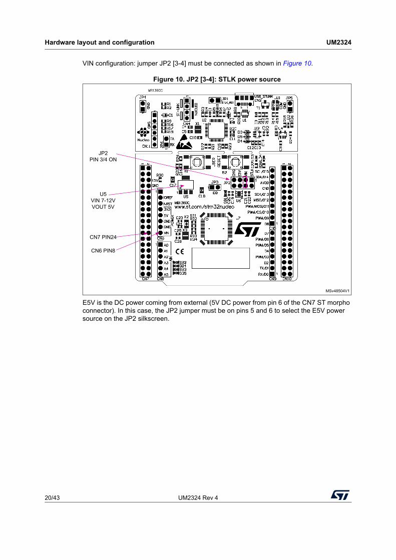
VIN is the 7 V to 12 V DC power from CN6 pin 8 named VIN on ARDUINO® connector silkscreen or from pin 24 of CN7 ST morpho connector. In this case, the JP2 jumper must be on pins 3 and 4 to select the VIN power source on the JP2 silkscreen. In that case, the DC power comes from the power supply through the ARDUINO® Uno V3 battery shield (compatible with Adafruit PowerBoost 500 shield).
MSv48503V1
CN2USB_STLINK
JP2PIN 1/2 ON
Hardware layout and configuration UM2324
20/43 UM2324 Rev 4
VIN configuration: jumper JP2 [3-4] must be connected as shown in Figure 10.
Figure 10. JP2 [3-4]: STLK power source
E5V is the DC power coming from external (5V DC power from pin 6 of the CN7 ST morpho connector). In this case, the JP2 jumper must be on pins 5 and 6 to select the E5V power source on the JP2 silkscreen.
MSv48504V1
U5VIN 7-12VVOUT 5V
JP2PIN 3/4 ON
CN7 PIN24
CN6 PIN8

UM2324 Rev 4 21/43
UM2324 Hardware layout and configuration
42
E5V configuration: Jumper JP2 [5-6] must be connected as shown in Figure 11.
Figure 11. JP2 [5-6]: STLK power source
5V_USB_CHARGER is the DC power charger connected to USB ST-LINK (CN2). To select the CHG power source on the JP2 silkscreen, the JP2 jumper must be on pins 7 and 8. In this case, if the STM32 Nucleo-64 board is powered by an external USB charger the debug is not available. If the PC is connected instead of the charger, the limitation is no more effective and the PC can be damaged.
MSv48505V1
E5V: CN7 PIN6
JP2PIN 5/6 ON

Hardware layout and configuration UM2324
22/43 UM2324 Rev 4
CHG configuration: jumper JP2 [7-8] must be connected as shown in Figure 12.
Figure 12. JP2 [7-8]: CHG power source
6.5.2 External power supply output:
• 5V: The 5V (CN6 pin 5 or CN7 pin 18) is usable as an output power supply for an ARDUINO® shield or an extension board when the STM32 Nucleo-64 board is powered by USB, VIN, or E5V. In this case, the maximum current allowed is shown in Table 7.
• 3.3V: on CN6 pin 4 or CN7 pin 16 is usable as power supply output. The current is limited by the maximum current capability of the regulator U6 (LDL112PV33R from STMicroelectronics). In this condition, the maximum consumption of the STM32 Nucleo-64 board and the connected shield must be less than 500 mA.
6.6 Programming/debugging when the power supply is not from ST-LINK
VIN or E5V is usable as an external power supply in case the current consumption of the STM32 Nucleo-64 board and its extension boards exceed the allowed current on the USB. In such a condition, it is still possible to use the USB for communication, programming, or debugging only. In this case, it is mandatory to power the board first using VIN or E5V then to connect the USB cable to the PC. Proceeding this way the enumeration succeeds, thanks to the external power source. The following power sequence procedure must be respected:
MSv48506V1
CN2USB STLK
JP2PIN 7/8 ON
UM2324 Rev 4 23/43
UM2324 Hardware layout and configuration
42
1. Connect jumper JP2 between pins 3 and 4 for VIN or pins 5 and 6 for E5V,
2. Connect the external power source to VIN or E5V,
3. Power ON the external power supply 7 V < VIN < 12 V to VIN, or 5 V for E5V,
4. Check that the green LED LD3 is turned ON,
5. Connect the PC to the CN2 USB connector.
If this sequence is not respected, the board may be powered by VBUS first from the ST-LINK, with the following risks:
• If more than 500 mA current is needed by the board, the PC may be damaged or the current supplied may be limited by the PC. As a consequence, the board is not powered correctly.
• 500 mA is requested at the enumeration (since SB15 must be OFF): this request is rejectable and the enumeration does not succeed if the PC does not provide such current, consequently, the board is not power supplied (LED LD3 remains OFF).
6.7 OSC clock sources
Three clock sources are listed below:
• LSE which is the 32.768 kHz crystal for the STM32 embedded RTC
• MCO which is the 8 MHz clock from the ST-LINK MCU for the STM32 microcontroller
• HSE which is the 8 MHz oscillator for the STM32 microcontroller. This clock is not implemented on the STM32 Nucleo-64 board
6.7.1 LSE: OSC 32 kHz clock supply
There are three ways to configure the pins corresponding to the low-speed clock (LSE):
1. LSE on-board X2 crystal (Default configuration). Refer to crystal design guide for STM8S, STM8A, and STM32 microcontrollers application note (AN2867) for crystal design guide for STM32 microcontrollers. It is recommended to use NX3215SA manufactured by NDK (32.768 kHz, 6 pF, 20 ppm).
2. Oscillator from external to PC14 input: from external oscillator through pin 25 of the CN7 connector. The following configuration is needed:
– SB23 ON
– R31 and R32 removed
3. LSE not used: PC14 and PC15 are used as GPIOs instead of low-speed clocks. The following configuration is needed:
– SB23 and SB24 ON
– R31 and R32 removed
Hardware layout and configuration UM2324
24/43 UM2324 Rev 4
6.7.2 HSE: OSC 8 MHz clock supply
There are four ways to configure the pins corresponding to the external high-speed clock (HSE):
• HSE not used (default): PF0 and PF1 are used as GPIOs instead of clocks. The configuration must be:
– SB25 and SB27 ON
– SB17 (MCO) OFF
– R33 and R34 OFF
• MCO from ST-LINK: MCO output of ST-LINK is used as an input clock. This frequency cannot be changed, it is fixed at 8 MHz and connected to the PF0-OSC_IN of the STM32 microcontroller. The configuration must be:
– SB17 ON
– SB25 and SB27 OFF
– R33 and R34 OFF
• HSE on-board oscillator from X3 crystal (not provided): for typical frequencies, capacitors, and resistors, refer to the STM32 microcontroller datasheet and the Oscillator design guide for STM8S, STM8A, and STM32 microcontrollers application note (AN2867) for the oscillator design guide. The X3 crystal has the following characteristics: 8 MHz, 8 pF, 20 ppm. It is recommended to use NX3225GD-8.000M- EXS00A-CG04874 manufactured by NIHON DEMPA KOGYO CO., LTD. The configuration must be:
– SB25 and SB27 OFF
– R33 and R34 soldered
– C24 and C25 soldered with 10 pF capacitors
– SB17 OFF
• Oscillator from external PF0: from an external oscillator through pin 29 of the CN7 connector. The configuration must be:
– SB25 ON
– SB17 OFF
– R33 and R34 removed
6.8 Reset sources
The reset signal of the STM32 Nucleo-64 board is active low and the reset sources include:
• B2 Reset button
• Embedded ST-LINK/V2-1
• Pin 3 of the CN6 ARDUINO® Uno V3 connector
• Pin 14 of the CN7 ST morpho connector
6.9 UART2 communication
The UART2 interface of the STM32 is connectible to:
• The ST-LINK/V2-1 MCU
• The ST morpho connector (CN10 pin 6 and pin 34)

UM2324 Rev 4 25/43
UM2324 Hardware layout and configuration
42
6.10 LEDs
Four LEDs are available on the STM32 Nucleo-64 board. The four LEDs are located on the top side of the board.
1. LD1 COM: LD1 is a bi-colored LED. the LD1 default status is red. LD1 turns to green to indicate that communication is in progress between the PC and the ST-LINK/V2-1 as follow:
– Slow blinking red and off: at power-on before USB initialization
– Fast blinking red and off: after the first correct communication between the PC and the STLINK/V2-1 (enumeration)
– Red LED on: when initialization between the PC and the ST-LINK/V2-1 is successfully ended
– Green LED on: after successful STM32 communication initialization
– Blinking red and green: during communication with STM32
– Green on: communication well ended
– Orange on: communication ended with failure
2. LD2: 5V_USB_CHG: this red LED is ON when overcurrent is detected on USB VBUS. The LED gives the information that more than 500 mA is requested on VBUS. In this case, it is recommended to supply the board with E5V, VIN, or in USB_CHARGER mode.
3. LD3: 5V_PWR: this green LED is ON when the STM32 Nucleo-64 board is powered by a 5 V source.
4. LD4 USER: this green LED is a user LED connected to ARDUINO® signal D13 corresponding to STM32 I/O PA5. To light the LED a high-logic state ‘1’ has to be written in the corresponding GPIO. A transistor is used to drive the LED when the I/O voltage is 1.8 V. LD4 consumption does not impact the VDD STM32 power measurement, since LD4 is isolated from it.
6.11 Push-buttons
• B1 USER: User and Wake-Up button connected to the I/O PC13 (Pin 3) of the STM32 Microcontroller.
• B2 RESET: Pushbutton connected to NRST is used to RESET the STM32 Microcontroller.
The blue and black plastic hats placed on these pushbuttons are removable if necessary when a shield or an application board is plugged on top of Nucleo. This avoids pressure on the buttons and consequently a possible permanent Target MCU RESET.
Table 8. UART2 pins
Pin name
FunctionVirtual COM port (default
configuration)ST morpho connection
PA2 UART2 TX SB16 ON SB16 OFF
PA3 UART2 RX SB18 ON SB18 OFF

Hardware layout and configuration UM2324
26/43 UM2324 Rev 4
6.12 IDD measurement
The JP3 labeled-IDD jumper allows the consumption of the STM32 Microcontroller to be measured by removing the jumper and connecting an ammeter.
• Jumper ON: STM32 Microcontroller is powered (default).
• Jumper OFF: an ammeter must be connected to measure the STM32 microcontroller current. If there is no ammeter, the STM32 microcontroller is not powered.
6.13 Jumper configuration
The default jumper positions are shown inTable 4. Table 9 describes the other available jumper settings.
6.14 Configuration of the solder bridges
Table 10 shows the solder bridge configurations and settings.
Table 9. Jumper configuration
Jumper / CN
Function State(1)
1. Default jumper state is shown in bold.
Comment
CN4T_SWCLK T_SWDIO
ON [1-2] ON [3-4]ST-LINK/V2-1 enable for on-board MCU debugger
OFF [1-2] OFF [3-4]ST-LINK/V2-1 functions enabled for external CN2 connector
JP4/JP5 GND ON GND probe
JP25 V Power selection
ON [1-2] 5 V from ST-LINK
ON [3-4] 5 V from VIN 7 V to 12 V
ON [5-6] 5 V from E5V
ON [7-8] 5 V from USB_CHG
OFF No 5 V power
JP1 STLK ResetON [1-2] STLK Reset
OFF No STLK Reset
JP3 IDD measurement
ON [1-2] VDD = 3.3 V
OFFTo connect the external source (ULPBench probe as an example)
Table 10. Solder bridge configurations and settings
Definition Bridge State(1) Comment
SWD interface (default))
SB7/SB9 /SB11/SB13
ON Reserved, do not modify.
SWD interface (reserved)
SB6/SB8 /SB10/SB12
OFF Reserved, do not modify.
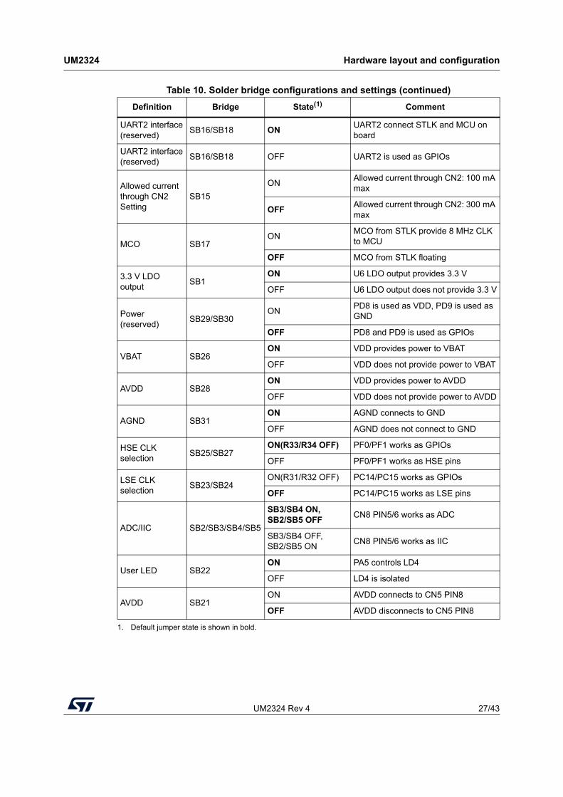
UM2324 Rev 4 27/43
UM2324 Hardware layout and configuration
42
UART2 interface (reserved)
SB16/SB18 ONUART2 connect STLK and MCU on board
UART2 interface (reserved)
SB16/SB18 OFF UART2 is used as GPIOs
Allowed current through CN2 Setting
SB15
ONAllowed current through CN2: 100 mA max
OFFAllowed current through CN2: 300 mA max
MCO SB17ON
MCO from STLK provide 8 MHz CLK to MCU
OFF MCO from STLK floating
3.3 V LDO output
SB1ON U6 LDO output provides 3.3 V
OFF U6 LDO output does not provide 3.3 V
Power (reserved)
SB29/SB30ON
PD8 is used as VDD, PD9 is used as GND
OFF PD8 and PD9 is used as GPIOs
VBAT SB26ON VDD provides power to VBAT
OFF VDD does not provide power to VBAT
AVDD SB28ON VDD provides power to AVDD
OFF VDD does not provide power to AVDD
AGND SB31ON AGND connects to GND
OFF AGND does not connect to GND
HSE CLK selection
SB25/SB27ON(R33/R34 OFF) PF0/PF1 works as GPIOs
OFF PF0/PF1 works as HSE pins
LSE CLK selection
SB23/SB24ON(R31/R32 OFF) PC14/PC15 works as GPIOs
OFF PC14/PC15 works as LSE pins
ADC/IIC SB2/SB3/SB4/SB5
SB3/SB4 ON, SB2/SB5 OFF
CN8 PIN5/6 works as ADC
SB3/SB4 OFF, SB2/SB5 ON
CN8 PIN5/6 works as IIC
User LED SB22ON PA5 controls LD4
OFF LD4 is isolated
AVDD SB21ON AVDD connects to CN5 PIN8
OFF AVDD disconnects to CN5 PIN8
1. Default jumper state is shown in bold.
Table 10. Solder bridge configurations and settings (continued)
Definition Bridge State(1) Comment

Connectors UM2324
28/43 UM2324 Rev 4
7 Connectors
Seven connectors are implemented on the STM32 Nucleo-64 board:
• CN2: ST-LINK USB connector
• CN5, CN6, CN8, and CN9: ARDUINO® Uno V3 connector
• CN7 and CN10: ST morpho connectors
7.1 CN2 USB Micro-B connector
The CN2 USB connector is used to connect the embedded ST-LINK/V2-1 to the PC for programming and debugging the STM32 Nucleo-64 board microcontroller.
Figure 13. CN2 USB Micro-B connector (front view)
The related pinout for the USB ST-LINK connector is listed in Table 11.
Table 11. USB Micro-B pinout
ConnectorPin
numberPin
nameSignal name
ST-LINKMCU pin
Function
CN2
1 VBUS5V_STLINK / 5V_USB_CHG
- 5 V power
2 DM (D-) STLINK_USB_D_N PA11 USB diff. pair M
3 DP (D+) STLINK_USB_D_P PA12 USB diff. pair P
4 ID - - -
5 GND - - GND
MSv46073V1

UM2324 Rev 4 29/43
UM2324 Connectors
42
7.2 ARDUINO® Uno V3 connector
The CN5, CN6, CN8, and CN9 ARDUINO® connectors in Figure 14 are female connectors compatible with the ARDUINO® standard. Most shields designed for ARDUINO® fit the STM32 Nucleo-64 board.
The ARDUINO® connectors on the STM32 Nucleo-64 board support the ARDUINO® Uno V3.
Figure 14. ARDUINO® connectors
MSv48507V2
CN6:Arduino_PWR
CN8:Arduino_A[0..5]
CN5:Arduino_D[8..15]
CN9:Arduino_D[0..7]

Connectors UM2324
30/43 UM2324 Rev 4
The related pinout for the ARDUINO® connector is shown in Figure 15 and Figure Note: and listed in Table 12.
Figure 15. STM32 Nucleo-64 boards ARDUINO® connector pinout
Note: ARDUINO® Uno V3 D0 and D1 signals are connected by default on USART1 (MCU I/O PC4 and PC5).
Table 12. ARDUINO® connector pinout
ConnectorPin
numberPin
nameSignal name STM32 pin Function
CN6
1 NC - - Reserved for test
2 IOREF - - I/O reference
3 NRST NRST NRST RESET
4 3V3 - - 3.3 V input/output
5 5V - - 5 V output
6 GND - - GND
7 GND - - GND
8 VIN - - 7 V to 12 V power input
CN8
1 A0 ADC PA0 ARD_A0_IN0
2 A1 ADC PA1 ARD_A1_IN1
3 A2 ADC PA4 ARD_A2_IN4
4 A3 ADC PB1 ARD_A3_IN9
5 A4 ADC PB9 or PB11 ARD_A4_IN15|| I2C_1_SCL
6 A5 ADC PB8 or PB12 ARD_A5_IN16|| I2C_1_SDA

UM2324 Rev 4 31/43
UM2324 Connectors
42
CN5
10 SCL/D15 ARD_D15 PB8 I2C_1_SCL
9 SDA/D14 ARD_D14 PB9 I2C_1_SDA
8 AVDD VREF+ - VREF+
7 GND - - GND
6 SCK/D13 ARD_D13 PA5 SPI_1_SCK
5 MISO/D12 ARD_D12 PA6 SPI_1_MISO
4 PWM/MOSI/D11 ARD_D11 PA7 SPI_1_MOSI || TIM_14_CH1
3 PWM/CS/D10 ARD_D10 PB0 SPI_1_NSS || TIM_3_CH3
2 PWM/D9 ARD_D9 PC7 TIM_3_CH2
1 D8 ARD_D8 PA9 IO
CN9
8 D7 ARD_D7 PA8 IO
7 PWM/D6 ARD_D6 PB14 TIM_15_CH1
6 PWM/D5 ARD_D5 PB4 TIM_3_CH1
5 D4 ARD_D4 PB5 IO
4 PWM/D3 ARD_D3 PB3 TIM_1_CH2
3 D2 ARD_D2 PA10 IO
2 TX/D1 ARD_D1 PC4 UART_1_TX
1 RX/D0 ARD_D0 PC5 UART_1_RX
Table 12. ARDUINO® connector pinout (continued)
ConnectorPin
numberPin
nameSignal name STM32 pin Function

Connectors UM2324
32/43 UM2324 Rev 4
7.3 CN7 and CN10 ST morpho connectors
The CN7 and CN10 ST morpho connectors are male pin headers accessible on both sides of the STM32 Nucleo-64 board (see Figure 16). All signals and power pins, except VDD_CORE 1.2 V of the STM32, are available on the ST morpho connectors. These connectors can also be probed by an oscilloscope, logical analyzer, or voltmeter.
Figure 16. ST morpho connectors
MSv48509V2
CN7:ST morpho connector
CN10:ST morpho connector
UM2324 Rev 4 33/43
UM2324 Connectors
42
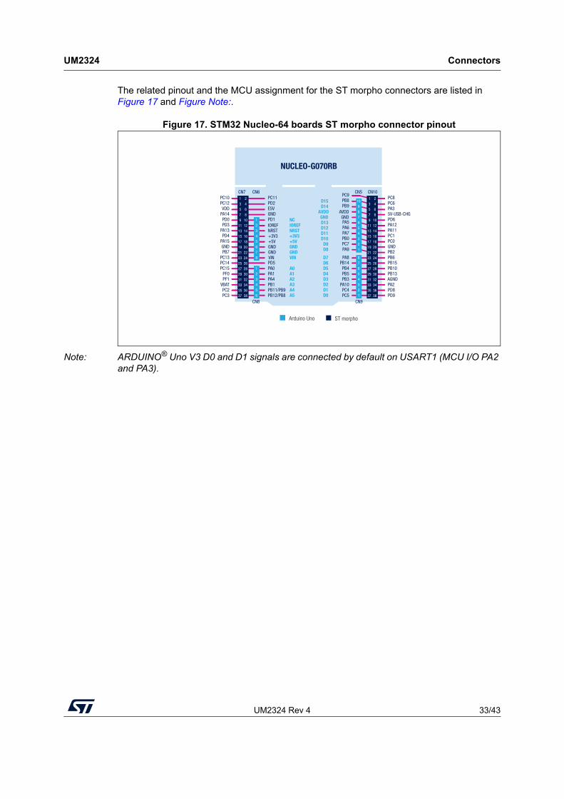
The related pinout and the MCU assignment for the ST morpho connectors are listed in Figure 17 and Figure Note:.
Figure 17. STM32 Nucleo-64 boards ST morpho connector pinout
Note: ARDUINO® Uno V3 D0 and D1 signals are connected by default on USART1 (MCU I/O PA2 and PA3).

STM32 Nucleo-64 board information UM2324
34/43 UM2324 Rev 4
8 STM32 Nucleo-64 board information
8.1 Product marking
The stickers located on the top or bottom side of the PCB provide product information:
• Product order code and product identification for the first sticker
• Board reference with revision, and serial number for the second sticker
On the first sticker, the first line provides the product order code, and the second line the product identification.
On the second sticker, the first line has the following format: “MBxxxx-Variant-yzz”, where “MBxxxx” is the board reference, “Variant” (optional) identifies the mounting variant when several exist, "y" is the PCB revision and "zz" is the assembly revision, for example B01. The second line shows the board serial number used for traceability.
Evaluation tools marked as “ES” or “E” are not yet qualified and therefore not ready to be used as reference design or in production. Any consequences deriving from such usage will not be at ST charge. In no event, ST will be liable for any customer usage of these engineering sample tools as reference designs or in production.
“E” or “ES” marking examples of location:
• On the targeted STM32 that is soldered on the board (For an illustration of STM32 marking, refer to the STM32 datasheet “Package information” paragraph at the www.st.com website).
• Next to the evaluation tool ordering part number that is stuck or silk-screen printed on the board.
Some boards feature a specific STM32 device version, which allows the operation of any bundled commercial stack/library available. This STM32 device shows a "U" marking option at the end of the standard part number and is not available for sales.
In order to use the same commercial stack in his application, a developer may need to purchase a part number specific to this stack/library. The price of those part numbers includes the stack/library royalties.
8.2 NUCLEO-G070RB product history
8.2.1 Product identification NUG070RB$AU1
This product identification is based on the MB1360-G070RB-C01 board.
It embeds the STM32G070RBT6 microcontroller with silicon revision code "B". The limitations of this silicon revision are detailed in the errata sheet STM32G070CB/KB/RB device errata (ES0468).
Product limitations
No limitation identified for this product identification.
8.2.2 Product identification NUG070RB$AU2
This product identification is based on the MB1360-G070RB-C02 board.

UM2324 Rev 4 35/43
UM2324 STM32 Nucleo-64 board information
42
It embeds the STM32G070RBT6 microcontroller with silicon revision code "B". The limitations of this silicon revision are detailed in the errata sheet STM32G070CB/KB/RB device errata (ES0468).
Product limitations
No limitation identified for this product identification.
8.3 NUCLEO-G071RB product history
8.3.1 Product identification NUG071RB$AU1
This product identification is based on the MB1360-G071RB-C01 board.
It embeds the STM32G071RBT6 microcontroller with silicon revision code "B". The limitations of this silicon revision are detailed in the errata sheet STM32G071xx device errata (ES0418).
Product limitations
No limitation identified for this product identification.
8.3.2 Product identification NUG071RB$AU2
This product identification is based on the MB1360-G071RB-C02 board.
It embeds the STM32G071RBT6 microcontroller with silicon revision code "B". The limitations of this silicon revision are detailed in the errata sheet STM32G071xx device errata (ES0418).
Product limitations
No limitation identified for this product identification.
8.4 NUCLEO-G0B1RE product history
8.4.1 Product identification NUG0B1RE$AU1
This product identification is based on the MB1360-G0B1RE-C02 board.
It embeds the STM32G0B1RET6 microcontroller with silicon revision code "A". The limitations of this silicon revision are detailed in the errata sheet STM32G0B1xB/xC/xE device errata (ES0548).
Product limitations
No limitation identified for this product identification.
STM32 Nucleo-64 board information UM2324
36/43 UM2324 Rev 4
8.5 Board revision history
8.5.1 Board MB1360 revision C-01
The revision C-01 is the initial release of the MB1360 board.
This revision C-01 is produced with the STM32G070RBT6 or STM32G071RBT6 microcontroller.
Board limitations
No limitation identified for this board revision.
8.5.2 Board MB1360 revision C-02
C23 and C24 are modified from 5.6 pF to 6.8 pF.
T2 is modified from BSN20 to BSN20BK.
This revision C-02 is produced with the STM32G070RBT6, STM32G071RBT6, or the latest STM32G0B1RET6 microcontroller.
Board limitations
No limitation identified for this board revision.

UM2324 Rev 4 37/43
UM2324 STM32 Nucleo-64 board I/O assignment
42
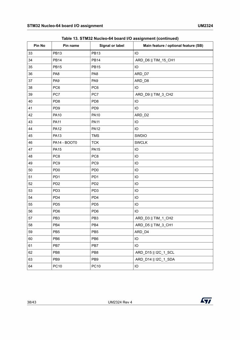
Appendix A STM32 Nucleo-64 board I/O assignment
Table 13. STM32 Nucleo-64 board I/O assignment
Pin No Pin name Signal or label Main feature / optional feature (SB)
1 PC11 PC11 IO
2 PC12 PC12 IO
3 PC13 PC13 User Button/IO
4 PC14 - OSC32_IN PC14 - OSC32_IN LSE CLK/IO
5 PC15 - OSC32_OUT PC15 - OSC32_OUT LSE CLK/IO
6 PF3 - VBAT VBAT PWR VBAT
7 PF4 - VREF+ AVDD PWR AVDD
8 VDD_1 VDD PWR VDD
9 VSS_1 GND PWR GND
10 PF0 - OSC_IN PF0 - OSC_IN HSE CLK/IO
11 PF1 - OSC_OUT PF1 - OSC_OUT HSE CLK/IO
12 PF2 - NRST PF2 - NRST RESET
13 PC0 PC0 IO
14 PC1 PC1 IO
15 PC2 PC2 IO
16 PC3 PC3 IO
17 PA0 PA0 ARD_A0_IN0
18 PA1 PA1 ARD_A1_IN1
19 PA2 UART2_TX STLK_RX
20 PA3 UART2_RX STLK_TX
21 PA4 PA4 ARD_A2_IN4
22 PA5 PA5 ARD_D13 || SPI_1_SCK
23 PA6 PA6 ARD_D12 || SPI_1_MISO
24 PA7 PA7 ARD_D11 || SPI_1_MOSI || TIM_14_CH1
25 PC4 PC4 ARD_D1 || UART_1_TX
26 PC5 PC5 ARD_D0 || UART_1_RX
27 PB0 PB0 ARD_D10 || SPI_1_NSS || TIM_3_CH3
28 PB1 PB1 ARD_A3_IN9
29 PB2 PB2 IO
30 PB10 PB10 IO
31 PB11 PB11 ARD_A4_IN15
32 PB12 PB12 ARD_A5_IN16
STM32 Nucleo-64 board I/O assignment UM2324
38/43 UM2324 Rev 4
33 PB13 PB13 IO
34 PB14 PB14 ARD_D6 || TIM_15_CH1
35 PB15 PB15 IO
36 PA8 PA8 ARD_D7
37 PA9 PA9 ARD_D8
38 PC6 PC6 IO
39 PC7 PC7 ARD_D9 || TIM_3_CH2
40 PD8 PD8 IO
41 PD9 PD9 IO
42 PA10 PA10 ARD_D2
43 PA11 PA11 IO
44 PA12 PA12 IO
45 PA13 TMS SWDIO
46 PA14 - BOOT0 TCK SWCLK
47 PA15 PA15 IO
48 PC8 PC8 IO
49 PC9 PC9 IO
50 PD0 PD0 IO
51 PD1 PD1 IO
52 PD2 PD2 IO
53 PD3 PD3 IO
54 PD4 PD4 IO
55 PD5 PD5 IO
56 PD6 PD6 IO
57 PB3 PB3 ARD_D3 || TIM_1_CH2
58 PB4 PB4 ARD_D5 || TIM_3_CH1
59 PB5 PB5 ARD_D4
60 PB6 PB6 IO
61 PB7 PB7 IO
62 PB8 PB8 ARD_D15 || I2C_1_SCL
63 PB9 PB9 ARD_D14 || I2C_1_SDA
64 PC10 PC10 IO
Table 13. STM32 Nucleo-64 board I/O assignment (continued)
Pin No Pin name Signal or label Main feature / optional feature (SB)

UM2324 Rev 4 39/43
UM2324 Federal Communications Commission (FCC) and ISED Canada Compliance Statements
42
Appendix B Federal Communications Commission (FCC) and ISED Canada Compliance Statements
B.1 FCC Compliance Statement
Part 15.19
This device complies with Part 15 of the FCC Rules. Operation is subject to the following two conditions: (1) this device may not cause harmful interference, and (2) this device must accept any interference received, including interference that may cause undesired operation.
Part 15.21
Any changes or modifications to this equipment not expressly approved by STMicroelectronics may cause harmful interference and void the user’s authority to operate this equipment.
Part 15.105
This equipment has been tested and found to comply with the limits for a Class B digital device, pursuant to part 15 of the FCC Rules. These limits are designed to provide reasonable protection against harmful interference in a residential installation. This equipment generates uses and can radiate radio frequency energy and, if not installed and used in accordance with the instructions, may cause harmful interference to radio communications. However, there is no guarantee that interference will not occur in a particular installation. If this equipment does cause harmful interference to radio or television reception, which can be determined by turning the equipment off and on, the user is encouraged to try to correct the interference by one or more of the following measures:
• Reorient or relocate the receiving antenna.
• Increase the separation between the equipment and the receiver.
• Connect the equipment into an outlet on a circuit different from that to which the receiver is connected.
• Consult the dealer or an experienced radio/TV technician for help.
Note: Use only shielded cables.
Responsible party (in the USA)
Terry Blanchard Americas Region Legal | Group Vice President and Regional Legal Counsel, The Americas STMicroelectronics, Inc. 750 Canyon Drive | Suite 300 | Coppell, Texas 75019 USA Telephone: +1 972-466-7845

Federal Communications Commission (FCC) and ISED Canada Compliance Statements UM2324
40/43 UM2324 Rev 4
B.2 ISED Compliance Statement
This device complies with FCC and ISED Canada RF radiation exposure limits set forth for general population for mobile application (uncontrolled exposure). This device must not be collocated or operating in conjunction with any other antenna or transmitter.
Compliance Statement
Notice: This device complies with ISED Canada licence-exempt RSS standard(s). Operation is subject to the following two conditions: (1) this device may not cause interference, and (2) this device must accept any interference, including interference that may cause undesired operation of the device.
ISED Canada ICES-003 Compliance Label: CAN ICES-3 (B) / NMB-3 (B).
Déclaration de conformité
Avis: Le présent appareil est conforme aux CNR d'ISDE Canada applicables aux appareils radio exempts de licence. L'exploitation est autorisée aux deux conditions suivantes : (1) l'appareil ne doit pas produire de brouillage, et (2) l'utilisateur de l'appareil doit accepter tout brouillage radioélectrique subi, même si le brouillage est susceptible d'en compromettre le fonctionnement.
Étiquette de conformité à la NMB-003 d'ISDE Canada : CAN ICES-3 (B) / NMB-3 (B).

UM2324 Rev 4 41/43
UM2324 CE conformity
42
Appendix C CE conformity
C.1 Warning
EN 55032 / CISPR32 (2012) Class B product
Warning: this device is compliant with Class B of EN 55032 / CISPR32. In a residential environment, this equipment may cause radio interference.
Avertissement : cet équipement est conforme à la Classe B de la EN 55032 / CISPR 32. Dans un environnement résidentiel, cet équipement peut créer des interférences radio.
C.2 Simplified declaration of conformity
Hereby, STMicroelectronics declares that the radio equipment types NUCLEO-G070RB and NUCLEO-G071RB comply with the applicable CE requirements stated below:
• EN 55032 (2012) / EN 55024 (2010)
• EN 60950-1 (2006 + A11/2009 + A1/2010 + A12/2011 + A2/2013)
Hereby, STMicroelectronics declares that the radio equipment type NUCLEO-G0B1REB complies with the applicable CE requirements stated below:
• EN 55032 (2012/2015) / EN 55035 (2017)
• EN 60950-1 (2006 + A11/2009 + A1/2010 + A12/2011 + A2/2013) / EN 62368-1 (2014 +A1/2017)
The complete declaration of conformity is available upon request from STMicroelectronics.

Revision history UM2324
42/43 UM2324 Rev 4
Revision history
Table 14. Document revision history
Date Revision Changes
24-Oct-2018 1 Initial version
26-Oct-2018 2 Added NUCLEO-G070RB board
19-Nov-2020 3
Added NUCLEO-G0B1RE board
Entire document reorganized
– Updated: Introduction, Features, Ordering information, Development environment, Development toolchains, and Demonstration software.
– Added: Codification, Section 8: STM32 Nucleo-64 board information, Appendix B: Federal Communications Commission (FCC) and ISED Canada Compliance Statements, and Appendix C: CE conformity.
– Removed Electrical schematics
8-Mar-2021 4
Updated:
– Figure 2: Hardware block diagram
– Section 8: STM32 Nucleo-64 board information

UM2324 Rev 4 43/43
UM2324
43
IMPORTANT NOTICE – PLEASE READ CAREFULLY
STMicroelectronics NV and its subsidiaries (“ST”) reserve the right to make changes, corrections, enhancements, modifications, and improvements to ST products and/or to this document at any time without notice. Purchasers should obtain the latest relevant information on ST products before placing orders. ST products are sold pursuant to ST’s terms and conditions of sale in place at the time of order acknowledgement.
Purchasers are solely responsible for the choice, selection, and use of ST products and ST assumes no liability for application assistance or the design of Purchasers’ products.
No license, express or implied, to any intellectual property right is granted by ST herein.
Resale of ST products with provisions different from the information set forth herein shall void any warranty granted by ST for such product.
ST and the ST logo are trademarks of ST. For additional information about ST trademarks, please refer to www.st.com/trademarks. All other product or service names are the property of their respective owners.
Information in this document supersedes and replaces information previously supplied in any prior versions of this document.
© 2021 STMicroelectronics – All rights reserved

Mouser Electronics
Authorized Distributor
Click to View Pricing, Inventory, Delivery & Lifecycle Information: STMicroelectronics:
NUCLEO-G0B1RE