Embed Size (px)
Citation preview

StimDust: A 6.5mm3, Wireless Ultrasonic PeripheralNerve Stimulator with 82% Peak Chip Efficiency
Benjamin C. Johnson*, Konlin Shen*, David Piech*, M. Meraj Ghanbari*, Ka Yiu Li*, Ryan Neely*,Jose M. Carmena*, Michel M. Maharbiz/ l, and Rikky Muller"!
"University of California, Berkeley, Berkeley, CA 94704, USAtChan-Zuckerberg Biohub, San Francisco, CA 94158
Abstract-We present a 6.Smm3 , lOmg, wireless peripheralnerve stimulator. The stimulator is powered and controlledthrough ultrasound from an external transducer and utilizes asingle 7S0x7S0x7S0pm3 piezocrystal for downlink communica-tion, powering, and readout, reducing implant volume and mass.An IC with O.06mm2 active circuit area, designed in TSMC 6SnmLPCMOS process, converts harvested ultrasound to stimulationcharge with a peak efficiency of 82%. A custom wireless protocolthat does not require a clock or memory circuits reduces on-chippower to 4pW when not stimulating. The encapsulated stimulatorwas cuffed to the sciatic nerve of an anesthetized rodent anddemonstrated full-scale nerve activation in vivo. We achieve ahighly efficient and temporally precise wireless peripheral nervestimulator that is the smallest and lightest to our knowledge.
Index Terms-Stimulation, neuromodulation, peripheral nerve,ultrasound, backscatter, low-power wireless
I. INTRODUCTION
Peripheral nerve stimulators (PNSs) have shown promisein the symptomatic treatment a variety of disorders such aschronic pain , sleep apnea, incontinence, and arthritis [I] , [2].A primary technological barrier to widespread adoption ofperipheral nerve stimulators is the need for a wireless, mm-scale system that can be implanted through minimally invasiveprocedures. Recent PNS research has focused on the develop-ment of small volume, battery-less systems that are capable ofsafe and efficient power transfer centimeters into tissue [2]-[4]. Typically, PNSs only require a single electrode pair tostimulate the nerve. Recently, ultrasound has been proposedas an efficient way to power and communicate with mm-scale implants in deep tissue, resulting in significant volumereduction [2], [3]. Compared to RF at 2GHz, ultrasound energyat 2MHz has less attenuation through tissue (I dB/cm vs.3dB/cm), a higher FDA limit (7.2mW/mm2 vs. 0.lmW/mm2 ) ,
and smaller wavelength (0.75mm vs. 25mm) [I].We present a 10mg, 6.5mm3 peripheral nerve stimulator
that uses a single piezocrystal for power and bidirectionalcommunication with ultrasound, and efficiently converts re-ceived power to provide well-controlled stimulation to thenerve. The smallest volume stimulators [3], [4] have beenimplemented with passive components, providing inefficientvoltage-mode stimulation that is sensitive to received powerand electrode impedance. Active, multi-channel neurostim-ulators utilizing inductive coupling have achieved high ef-ficiencies [5], [6], but require em-scale coils and occupy
978-1-5386-2483-8/18/$31.00 ©2018 IEEE
Fig. 1. System illustration of the implantable device. The implant is wirelesslypowered via harvested ultrasound from a piezo crystal. By detectin g theenvelope of incomin g ultrasound , the stimulation IC dynamically reconfiguresstimulation pulse width, pulse interval , interphase gap, and amplitude.
larger volumes. This work scales down the volume of theimplant by using a single piezocrystal coupled to an IC andwireless protocol that achieves high efficiency and precision.High efficiency is achieved through a combination of protocoldesign, duty cycling, active rectification, and reducing the needfor high voltage compliance stimulation. For precision, thestimulation IC utilizes a current-mode stimulator to delivera well-controlled charge independent of electrode size andimpedance, which can be highly variable at small scales. Thestimulation waveform is dynamically reconfigurable via thestructure of the input ultrasound, rather than bit packets. Theprotocol enables sub-us temporal precision of the stimulationwaveform without the need for a clock, and an inherently highdynamic range of pulse widths and frequencies (e.g. f st im =0-2kHz), while minimizing complexity and therefore power.
II . SYSTEM ARCHITECTURE
Fig. I depicts the system concept. The implanted stimulationmote is cuffed to a peripheral (e.g. sciatic) nerve whilean external transducer powers and controls the mote withultrasound. The external transducer is driven by a customASIC that level-shifts the microcontroller-generated ultrasoundtransmit signal [7]. The maximum drive voltage of the ex-
StimlC
/ ;',ct;"d;;g- - - - - - - - -"I (....T~C~I~ --- - - - - '\
I I 1I I 20"" II I 1I I 1I I 1' 1I I ..\. 1I I 1
<PSIim(jJetedion w/reduced I t I' .:_h:e~v~a~ _ _ ....1 , /1
I PowerUp I set I setup I Stirn I interphaseI Short I set I setup I S I1 1 ampi!'ude 116clksl 1 lIi!{' I lamp I 16c1ksl I,m I1 '"to'@ I \') I ® I G) I \1! I @ I (i) I ® I G) I rP_Z+~t-'-----,l":f----'
pz'1\AAAAAAAAAI_ AAAA1\JI!INW------/tAAAAAAAAy AAAhAAAAI_ D: VVVVVVVVVr--iVVVV: 1 :: VVVVVVVVn VVVV:VVVVV: L-~t-'--L.....{_~
VDD~ 1 1 I mod~ latedl Iii 1 I ez-I 1 1 I PI I I I I I I
POR I I I -3us after l I I I I I I'I--------l 1r PZklSS 1 I I I I II 1'" I I " , I
WalChdOg~I~1 II II t 1 I I I I I ,
SIale: ~J: : U J: .Llit '- -' I '.'I- -'L
enGM 1 1 I I I I !I I I 1''--_ ';-'----:----!, 1 ,
",'m: :~ '----.r-L1 I 1 I I' . i I I
" """I I] 1 I 1 I I I I II I', I I[ electrode, I I ,1 I :~e~ISI~~e~ I short I I , I
• I~I ~1 I 1 I I I 1 I1 I 1 I I I 1 I
III . SYSTEM CHARACTERIZATION
The IC is fabricated in TSMC 65nm LP-CMOS processand occupies an area of Imm' (Fig. 3). The active area is150x400p,m2 . Fig. 3 also shows the mote assembly, whichmeasures 2x3.25x Imrn:' and 10mg. The height is dominatedby the 750p,m tall piezo and wire bond on a 100p,m-thickpolyimide PCB . A 4p,F 0201 surface mount capacitor isused to store energy for high-capacity stimulation. A IOrzm-thick conformal layer of parylene is used to encapsulatethe entire mote. A thin encapsulation layer ensures goodacoustical transmission between the surrounding tissue and thepiezo. The back of the mote features two 550x550p,m 2 Auelectrodes (stirn and return) electroplated with PEDOT:PSS.The PEDOT:PSS coating reduces the electrode imped anceseveral orders of magnitude at low frequency, reducing the
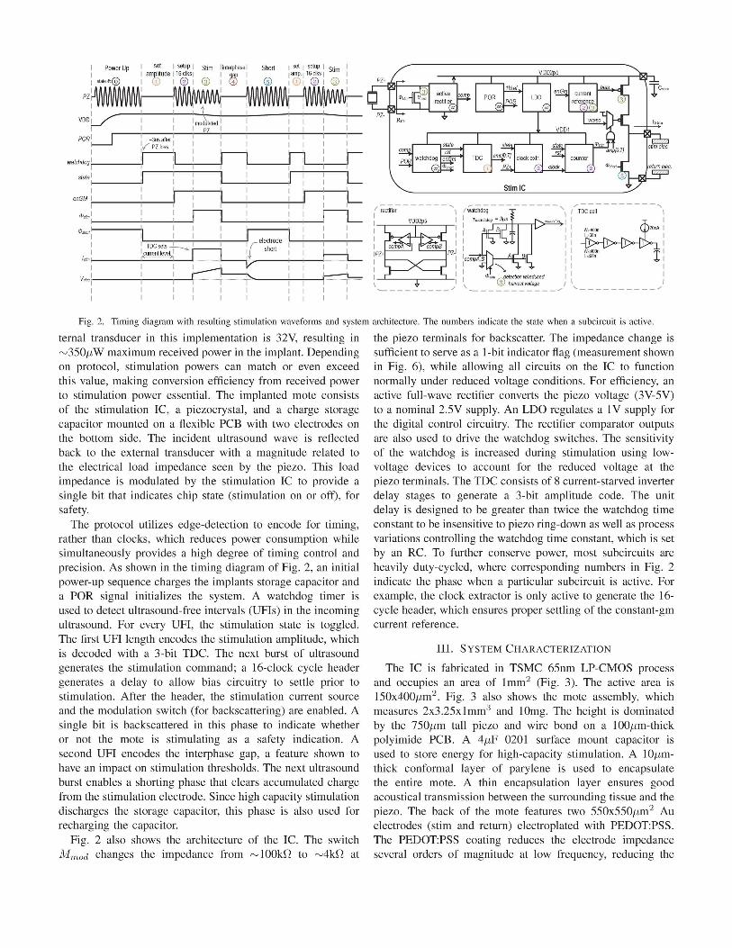
Fig. 2. Timing diagram with resulting stimulation waveform s and system architecture. The numbers indicate the state when a subcircuit is active .
ternal transducer in this implementation is 32V, resulting in the piezo terminals for backscatter. The impedance change isrv350p,W maximum received power in the implant. Depending sufficient to serve as a I-bit indicator flag (measurement shownon protocol, stimulation powers can match or even exceed in Fig. 6), while allowing all circuits on the IC to functionthis value, making conversion efficiency from received power normally under reduced voltage conditions. For efficiency, anto stimulation power essential. The implanted mote consists active full-wave rectifier converts the piezo voltage (3V-5V)of the stimulation IC, a piezocrystal , and a charge storage to a nominal 2.5V supply. An LDO regulates a IV supp ly forcapacitor mounted on a flexible PCB with two electrodes on the digital control circuitry. The rectifier comparator outputsthe bottom side. The incident ultrasound wave is reflected are also used to drive the watchdog switches. The sensitivityback to the external transducer with a magnitude related to of the watchdog is increased during stimulation using low-the electrical load impedance seen by the piezo. This load voltage devices to account for the reduced voltage at theimpedance is modulated by the stimulation IC to provide a piezo terminals. The TDC consists of 8 current-starved invertersingle bit that indicates chip state (stimulation on or off), for delay stages to generate a 3-bit amplitude code. The unitsafety. delay is designed to be greater than twice the watchdog time
The protocol utilizes edge -detection to encode for timing , constant to be insensitive to piezo ring-down as well as processrather than clocks, which reduces power consumption while variations controlling the watchdog time constant, which is setsimultaneously provides a high degree of timing control and by an Re. To further conserve power, most subcircuits areprecision. As shown in the timing diagram of Fig. 2, an initial heavily duty-cycled, where corresponding numbers in Fig. 2power-up sequence charges the implants storage capacitor and indicate the phase when a particular subcircuit is active. Fora POR signal initializes the system. A watchdog timer is example, the clock extractor is only active to generate the 16-used to detect ultrasound-free intervals (UFIs) in the incoming cycle header, which ensures proper settling of the constant-gmultrasound. For every UFI , the stimulation state is toggled . current reference.The first UFI length encodes the stimulation amplitude, whichis decoded with a 3-bit TDe. The next burst of ultrasoundgenerates the stimulation command; a 16-clock cycle headergenerates a delay to allow bias circuitry to settle prior tostimulation. After the header, the stimulation current sourceand the modulation switch (for backscattering) are enabled. Asingle bit is backscattered in this phase to indicate whetheror not the mote is stimulating as a safety indication. Asecond UFI encodes the interphase gap , a feature shown tohave an impact on stimulation thresholds. The next ultrasoundburst enables a shorting phase that clears accumulated chargefrom the stimulation electrode. Since high capacity stimulationdischarges the storage capacitor, this phase is also used forrecharging the capacitor.
Fig. 2 also shows the architecture of the K', The switchlv[m od changes the impedance from rvIOOkn to rv4kn at

2.2
100
1.8
so
I Stim,MAX
16
Rpiezo4kD,1.85MHz
Frequency (MHz)
82.8%••'.'.
Piezo Impdeance
8 2~'-'
2:l 1C »: ...rn l.-- - - - -. .' .'"0 0 -- ----- ----- -----; ._ ..,!'- ----- ---\- ---Q) " , •~ ,,' , ,E-1 •••••••• _ real v
......---- imaginary
tTDC.cell =8.21JS ± .271JS
40 60tgap(/lS)
I Stim,AVG = IStim,AMP X Tpulse X F Stim
20
[}kIN
~chip = (Pstim I Pin) x1 00
o
Chip RIN(n)
IIIIIII
Rpiezo:
Backscatter~
Mmod enableW
106Chip Input Impedance
,-.,
1M~e",bledc: 105'-'
Z~0.
:E 104U
I Stim,AVG = I Stim,AMP X T pulse X F Stim
103
10-1 10° 101 102
IS tim,AVG (IJA)
100
100 101
I Stim,AVG (IJA)
g soG53 60'u~
~ 400.
6 20
O-+n""'-><'---r"'-'rTT'I'TTT"----'r-T""TT'rTTl1r---r---T'""T'"rTT1,.,---'
1 400
'-' 350
15 300Q)
~ 250U 200"50. 150"5o 100
501-~~--.--,-~,.......,~--.--,--.--,.......,~---.--,--.--.,......,
Fig. 6. Measured chip input resistance versus stimulation load. Plot of theestimated backscatter profile based on measured chip input resistance andpiezo impedance .
Fig. 5. Stimulator output current plotted against TDC time and overall chipefficiency.
102
Frequency (Hz)
Series Electrode Impedance
TOP Ei(j
I/active area
BOnOM
103 +---.-....-TTTTrr--,-rT1Tmr--r-t-t-oTTTTn-r-rTTT-.m
10° 101
Fig. 3. Die microphotograph and board photographs .
- Gold- PEDOT:PSS
Fig. 4. tmpedance measurement of the electrodes in series before and afterelectroplating .
required stimulation headroom and eliminating the need forhigh voltage circuits, improving chip efficiency (Fig . 4). Fur-thermore, a lower supply voltage enables the use of higherdensity capacitors with lower voltage ratings.
Fig. 5 shows the measured output current versus UFI-length and the chip efficiency. While the relative error betweencurrent levels of the DAC or TDC steps is small, the absoluteerror will be sensitive to process variation. However, this iseasily calibrated by adjusting the protocol with the externalsystem. The overall chip efficiency (T]) is defined as thestimulation output power divided by the input power to thechip (82% at ISt irn ,A v e = 48{LA). The average stimulationcurrent is defined as IStirn,Ave = I S t irn ,AM p *TP ul s e *FS tirn '
When not stimulating, the DC power is measured to be 4{LW.When stimulating, the total power dissipation is roughly PTOT
=2.5V*Is t irn ,Ave I T] . Since implants are typically limited bythe amount of available power, the design is optimized forhigh efficiency for higher capacity stimulation.
In order to discriminate between shorting and stimulationstates at an external reader, the modulation switch ensuresa significant change in impedance. Backscatter amplitude ismodulated by the electrical impedance load on the piezo (chipR[ N; changes with chip load) . The impedance of the modu-lation switch is designed to approximate the series resonantresistance of the piezo , where the backscatter profile is mostsensitive to small change (Fig. 6). This allows for reader todistinguish between states even at a high load. The expectedbackscatter profile was simulated with a finite element method.
Fig. 7 shows in vitro results of the stimulation mote pow-ered and controlled via ultrasound near 1.85MHz, the piezoresonant frequency. The mote was suspended in ultrasound gelat the focal length of the extern al transducer (21.5mm). Thetransient results demonstrate the mote executing two different
I15
Ito
Io 5
T ime (ms)
average trials
T Pub..= 3 0 0 .US
150 200 250 300 350 400
Istim ( ~IA)
o 5T ime (ms)
pk-to-pk EMGvoltage-~-~
-5<0,100 200 300Time ( ~IS)
>'lsne 3 2
- 4 0 0 !1A "2 ~:~~~~r!: -'l---.J',,~~!!!"-\)_
- 150~ 0- 10 0 /!A ~ _4
- 50 )11\ I..il
'\-.-.~rrr......,~rrr"""'-rrrrr.,."~,, .6 f-.-~...~...,.,-'i'-.-~,..,...,~,..~,...,-100
- V Bar ksr,,1tr r
- V EI.EC
00Ti me (ms)
- PZ+- V DD2PS
:s '~,.
3~ '
" i=:==~11I 1I 1
L I: I : I
t~-,- L.. f "T''''T'-r-r-,-.r-r-r-j -r-r-r0 1 U 01
n. a_ 127
Time (ms)
O~ ..:
Iee
Time [ms)
I electrode
111 interphase gap , shorled
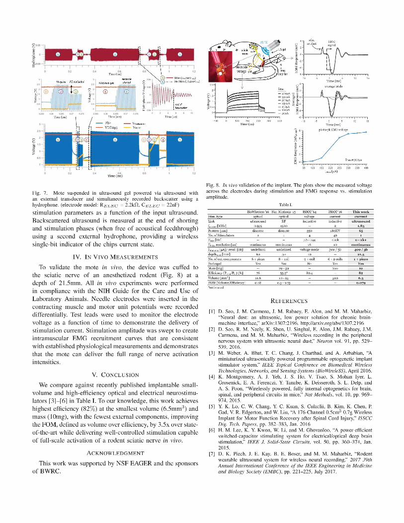
Fig. 7. Mote suspended in ultrasound gel powered via ultrasound withan external transducer and simultaneously recorded backscatter using ahydrophone. (electrode model: R EL E C = 2.2kO, C EL E C = 22nF)
stimulation parameters as a function of the input ultrasound.Backscattered ultrasound is measured at the end of shortingand stimulation phases (when free of acoustical feedthrough)using a second external hydrophone, providing a wirelesssingle-bit indicator of the chips current state.
IV. IN VIVO M EAS UREMENTS
To validate the mote in vivo, the device was cuffed tothe sciatic nerve of an anesthetized rodent (Fig. 8) at adepth of 2 I .5mm. All in vivo experiments were performedin compliance with the NIH Guide for the Care and Use ofLaboratory Animals. Needle electrodes were inserted in thecontracting muscle and motor unit potentials were recordeddifferentially. Test leads were used to monitor the electrodevoltage as a function of time to demonstrate the delivery ofstimulation current. Stimulation amplitude was swept to createintramuscular EMG recruitment curves that are consistentwith established physiological measurements and demonstratesthat the mote can deliver the full range of nerve activationintensities.
V. CONCLUSION
We compare agains t recently published implantable small-volume and high-efficiency optical and electrical neurostimu-lators [3]-[6] in Table 1. To our knowledge, this work achieveshighest efficiency (82%) at the smalle st volume (6.5mm3 ) andmass (I Omg), with the fewest external components, improvingthe FOM , defined as volume over efficiency, by 3.5x over state-of-the-art while delivering well-controlled stimulation capableof full-scale activation of a rodent sciatic nerve in vivo.
ACKNOWLEDGM ENT
This work was supported by NSF EAGER and the sponsorsof BWRC.
Fig. 8. In vivo validation of the implant. The plots show the measured voltageacross the electrodes during stimulation and EMG response vs. stimulationamplitude .
Table!.
Biowlreless tre Nat. Met hods '15 ISSCC '14 ISSCC '16 This wo rk
St irn. type opt ical op t ical voltag e cu rre nt cu rren tLink ult raso und RF induct ive indu ct ive ultrasound
f" " ,.. [MII, j 0 ·955 150 0 1.85
Process [001] discrete discrete 350 180 IIV 65No. of Stimu lators 4 40 .FSlim[II z] 7·6 - 244 <20k o-2k+
Tp lll,~ reso lution [us] continuous continuous .6 co ntinuous
ISlim.max [ IJA] / resol. [bit ] undefined undefined voltage mode 500 / 5b 400 /3bdepth lN x[0101] 60 30 10 21 ·5No. of ext . components 6 + piezo 8 + coil 9 + coil 6 + 2 coils :I.+ p lez oPackaged Yes Yes No Yes Ves
Mass [mg] 20 -50 70 0 10
Efficiency (P.lim/ Pin) [%] 76 33 ·3* 80 04 8.
Volu me [01013] 21.6 10- 25 500 6 .5FOM (Volume/ Efficiency) 0 .28 0 ·3 - 0·75 0.079"estimated
R EFERE NCES
[I] D. Seo, J. M. Carmena, J. M. Rabaey, E. Alon, and M. M. Maharbiz,"Neural dust: an ultrasonic, low power solution for chronic brain-machine interface ," arXiv:1307:2196. http://arxiv.org/abs/ 1307.2196
[2] D. Seo, R. M. Neely, K. Shen, U. Singhal, E. Alan, J.M. Rabaey, J.M.Carmena , and M. M. Maharbiz, "Wireless recording in the peripheralnervous system with ultrasonic neural dust," Neuro n vol. 91, pp. 529-539, 2016.
[3] M. Weber, A. Bhat, T. C. Chang, J. Charthad, and A. Arbabian, "Aminiaturized ultrasonically powered programmable optogenetic implantstimulator system," IEEE Topical Confe rence on Biomedical WirelessTechnologies. Ne tworks. and Sensing Systems (BioWireleSS) , April 2016.
[4] K. Montgomery, A. J. Yeh, J. S. Ho, V. Tsao, S. Mohan Iyer, L.Grosenick, E. A. Ferenczi, Y. Tanabe, K. Deisseroth, S. L. Delp, andA. S. Poon, "Wirelessly powered, fully internal optogenetics for brain,spinal, and peripheral circuits in mice," Nat Methods, vol. 10, pp. 969-974,2015.
[5] Y. K. Lo, C. W. Chang, Y. C. Kuan, S. Culaclii , B. Kim, K. Chen, P.Gad, V. R. Edgerton, and W. Liu, "A 176-Channel 0.5cm3 0.7g WirelessImplant for Motor Function Recovery after Spinal Cord Injury," ISSCCDig. Tech. Papers, pp. 382-383, Jan. 2016
[6] H. M. Lee, K. Y. Kwon, W. Li, and M. Ghovanloo, "A power-efficientswitched-capacitor stimulating system for electrical/optical deep brainstimulation," IEEE J. Solid -State Circuits, vol. 50, pp. 360-374, Jan.2015.
[7] D. K. Piech, J. E. Kay, B. E. Boser, and M. M. Maharbiz, "Rodentwearable ultrasound system for wireless neural recording," 2017 39thAnnual International Confe rence of the IEEE Engineering in Medicineand Biology Society (EMBC) , pp. 22 1-225 , July 2017.