Embed Size (px)
Citation preview

Status of the CSC Track-FinderStatus of the CSC Track-Finder
Darin Acosta
University of Florida

CMS Week, 25 Feb 2003
D.Acosta, University of Florida
2
CSC Muon Trigger SchemeCSC Muon Trigger Scheme
CSC
CFEBCFEBCFEB CFEB
ALCT1 of 24
CFEB
1 of 2
LVDB
1 of 5
1 of 5
Anode Front-end Board
Cathode Front-end Board
Anode LCT Board
MPC
DMB
TMB
DMB
TMB
DMB
TMB
DMB
TMB
DMB
TMB
DMB
TMB
DMB
TMB
DMB
TMB
DMB
TMB
CCBC
ONTROLLER
Peripheral Crate on iron disk (1 of 48)
Trigger Timing & Control
CSC Track-Finder Crate (1)
Trigger Motherboard (9)
DAQ Motherboard (9)Clock Control Board
Optical link
In underground counting room
On detector
Muon Portcard (1)
EMU part: mostly in productionTriDAS part: Second generation prototypes
Trigger Primitives
3-D Track-Finding and Measurement
Sector Processor (12)
Muon Sorter (1)

CMS Week, 25 Feb 2003
D.Acosta, University of Florida
3
11stst Prototype Track-Finder Tests (2000) Prototype Track-Finder Tests (2000)
Sector ProcessorSector Processor(Florida)(Florida)
Sector ReceiverSector Receiver(UCLA)(UCLA)
Clock Control Clock Control Board (Rice)Board (Rice)
Bit3 Bit3 VME VME InterfaceInterface
Custom Custom ChannelLinkChannelLinkBackplaneBackplane(Florida)(Florida)
Muon Port CardMuon Port Card(Rice)(Rice)
Very Very successful, successful, but overall but overall
CSC latency CSC latency was too high --was too high --
New 2002 New 2002 design design
improves improves latencylatency
Results included in Trigger L1 TDR

CMS Week, 25 Feb 2003
D.Acosta, University of Florida
4
CSC Track-Finder CrateCSC Track-Finder Crate
SR /
SP
SR /
SP
SR /
SP
SR /
SP
SR /
SP
SR /
SP
SR /
SP
SR /
SP
SR /
SP
SR /
SP
SR /
SP
SR /
SP
CC
B
SB
S 6
20 C
ontr
olle
r
Sector Processor
Clock and Control Board
Muon Sorter
From MPC (chamber 4)
From MPC (chamber 3)
From MPC (chamber 2)
From MPC (chamber 1B)
From MPC (chamber 1A)
To DAQ
MS
Single Track-Finder Crate Design with 1.6 Gbit/s optical links
Second generation prototypes
4 merged boards
CMS Week, 25 Feb 2003
D.Acosta, University of Florida
5
Combined SR/SP 2002 PrototypeCombined SR/SP 2002 Prototype
Problems encountered attempting layout using in-house tools
Sent to industry for completion of layout using Cadence Allegro
Final board takes 16 layers
Cost of manufacture, assembly, and parts is about $20K / board

CMS Week, 25 Feb 2003
D.Acosta, University of Florida
6
SP2002 Main Board (SR Logic)SP2002 Main Board (SR Logic)
3 SRs
Optical Transceivers
•15 x 1.6 Gbit/s Links
Front FPGA
TLK2501 Transceiver
Phi Local LUT
Eta Global LUT
Phi Global LUT
EEPROM
VME/CCB
FPGA
DC-DC Converter

CMS Week, 25 Feb 2003
D.Acosta, University of Florida
7
SP Trigger LogicSP Trigger Logic
From SP2000 to SP2002 mezzanine card
Xilinx Virtex-2 XC2V4000~800 user I/O
(Mezzanine card also used for CSC sorter)
CMS Week, 25 Feb 2003
D.Acosta, University of Florida
8
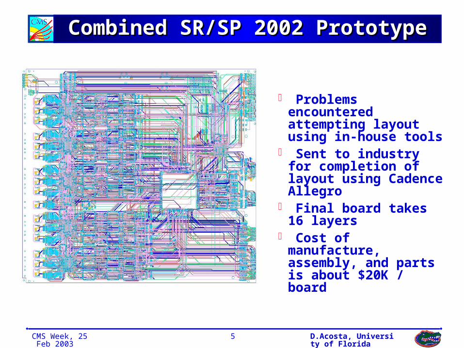
Tests underway…Tests underway…

CMS Week, 25 Feb 2003
D.Acosta, University of Florida
9
Optical Link Test ResultsOptical Link Test ResultsUsing pseudo-random test built into TLK2501 chipset
SP02 optical loopback test over 1 m optical cable No errors!
SP02 optical loopback test over 100 m cable BER = 1012
MPCSP02 optical test over 100 m cable BER = 3×10¹³
Controlled MPCSP02 chain test Download 255 bx of data for one MPC (3 muons × 32 bits),
preceding each iteration with a L1 Reset Send data over three 100 m cables into SP, and readout
Counting the 0’s transmitted between iterations, 30 link errors observed in total from 3 links over 16 hours (3×1014 bits) BER = 1013
Thus, about 1 error / hour, likely from clock jitter

CMS Week, 25 Feb 2003
D.Acosta, University of Florida
10
Optical Link Tests (Cont’d)Optical Link Tests (Cont’d)Controlled MPCSP02 chain test without L1 Reset
This is how we would like to operate Explicitly check data sent vs. data received Tests underway, code still needs improvements (e.g. to issue
L1 Reset if link fails and does not recover)

CMS Week, 25 Feb 2003
D.Acosta, University of Florida
11
ScheduleScheduleProposed schedule as of Feb-2003:
Feb.’03: SP02 prototype completed, initial tests begin Mar.’03: MPCSP optical link tests Apr.’03: SP memory and trigger logic tests May.’03: CSC system tests with cosmic rays and
beam tests at CERN
June ’03… : Tests with Muon Sorter and DT Track-Finder
√
√ (April)

CMS Week, 25 Feb 2003
D.Acosta, University of Florida
12
Test Beam PlansTest Beam PlansPlan to test CSC Trigger all the way to the Track-Finder in May/June beam tests Complete chain test from 2 detectors to peripheral crate
electronics to Track-Finder crate electronics!
Structured beam period: 23 May 1 June Two DAQ systems will run concurrently: CSC DAQ and
Track-Finder DAQ Track-Finder will just log inputs, not generate a track trigger Goal is to validate trigger primitives are found efficiently on
correct bx and successfully received over optical links Record as much data as possible under various detector
configurations for future track identification studies
Asynchronous beam period: 13 June 1 July Possibility to test a unified DAQ using “slice test” software
developed in XDAQ

CMS Week, 25 Feb 2003
D.Acosta, University of Florida
13
ConclusionsConclusionsSecond generation CSC Track-Finder prototype completed
Optical link tests between Port Card and Sector Receiver successful Measurable (but small ~10-13) bit error rate seen
Plan to take T-F to beam test later this monthTests of SR memories and SP trigger logic to followInterface tests with CSC Sorter and DT T-F also planned