Embed Size (px)
Citation preview

CMOS
Analog to Digital Converters :
State-of-the-Art and Perspectives
in Digital Communications
Hussein Fakhoury and Hervé Petit
C²S Research Group
ADC

Presentation Outline
Introduction
Basic concepts of A/D Conversion
ADC in digital radio receivers
Time-Interleaved ADC
Frequency synthesis for A/D Conversion

Introduction
The “practical” A/D Converter has 60 years old
1975
The first commercial ADC: “DATRAC” 11-bit, 50-kSPS SAR ADC (vacum tube)
Designed by Bernard M. Gordon at EPSCO
Dimensions: 48cmx38cmx66cm
Price : 8500$
Power : 500W
1954
“VHS 675” 6-bit, 75-MSPS FLASH ADC (hybrid ICs)
Designed by Computer Labs
Dimensions: 48cmx43cmx17cm
Price : 10000$
Power : 130W (linear power supplies included)

The first complete monolithic ADC “ADC 571”
10-bit, 40-kSPS SAR ADC in Bipolar Process
Designed by Analog Devices (Paul Brokaw)
Introduction
1978
The most power efficient DS ADC IP
~12-bit,BW=18MHz,3.9mW,0.08mm²
Designed by MediaTek in 28nm CMOS
2013
The “practical” A/D Converter has 60 years old

Basic concepts of A/D Conversion
‘1’
‘0’ ‘0’ ‘1’ N
quantization
noise
Modulated Signal x(t)
f f f
|X(f)| |X(f)| |X(f)|
fs -fs
Sampling
(fs>2xfb)
image
Due to quantization only (for a full-scale sine wave input):
SNR(dB)=6.02xN+1.76dB+10xlog(OSR)
Two fundamental steps Sampling : Shannon's theorem must be followed to avoid aliasing
Quantization : assumed to be an additive white noise process
Quantization
fb -fb
resolution Over-Sampling Ratio
fb -fb
clock signal (fs)
fb -fb
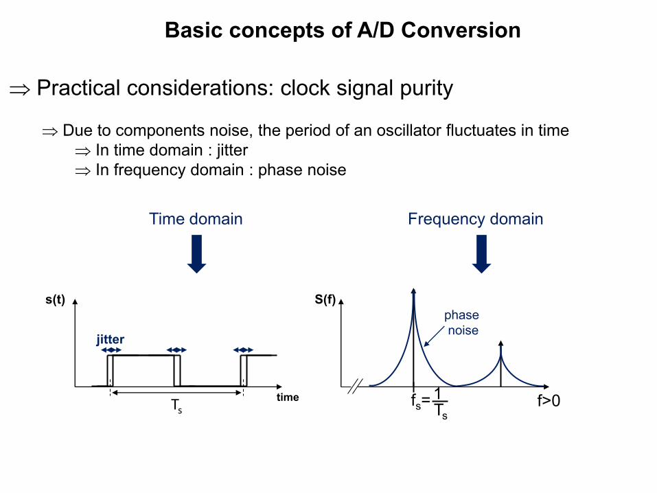
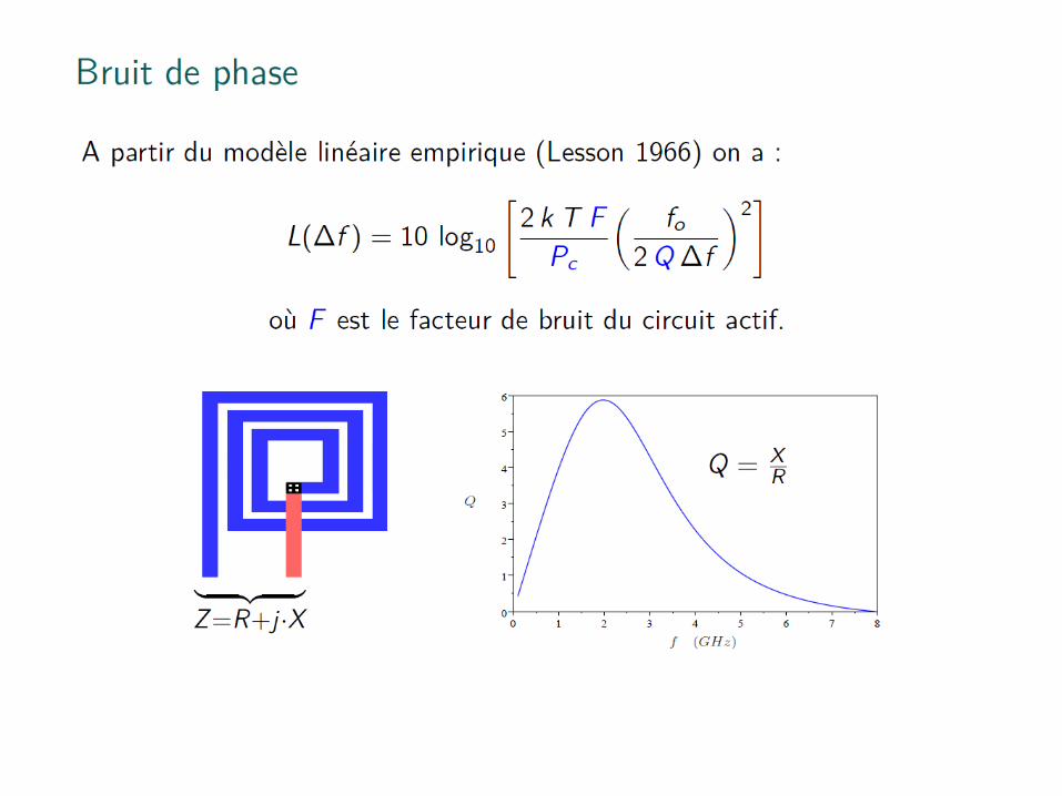
Practical considerations: clock signal purity
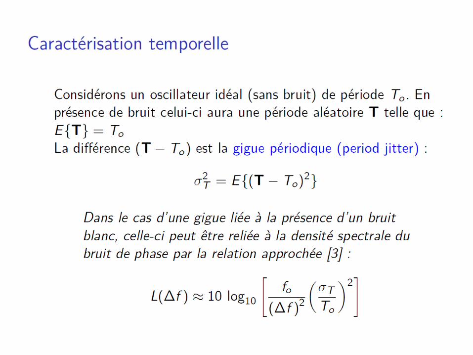
Due to components noise, the period of an oscillator fluctuates in time
In time domain : jitter
In frequency domain : phase noise
Time domain Frequency domain
Basic concepts of A/D Conversion
phase
noise
Ts
jitter
s(t)
time fs=
S(f)
f>0 Ts
1

Basic concepts of A/D Conversion
sinusoid input
x(t)
Sampling with
jittered-clock
Due to clock-jitter only (full-scale sine wave input) : SNRj=
Clock jitter is critical in wideband application !
Practical considerations: clock signal
Effect of clock jitter : in the time domain, the sampling process can bee seen as a
mixing of the input signal with the clock signal
Non-uniform sampling x(nTs+Ɛn)
f>0
|X(f)|
*
Signal corrupted
by phase noise
1
(2pfinsjitter)²
f>0 fs f>0 fin
phase noise
fin

Basic concepts of A/D Conversion
‘1’
‘0’ ‘0’ ‘1’ N
quantization noise
+ thermal noise
+ flicker noise
+ phase noise
+ distortion
Modulated Signal x(t)
f f f
|X(f)| |X(f)| |X(f)|
sampling
fb -fb
Effective resolution : SNDR=
+ thermal noise
+ flicker noise
+ phase noise
+ distortion
Practical considerations: components noise and distortion
Noise of active and passive components : thermal and flicker noise
Non-linear behavior of active components : harmonic distortion
Noise
+
quantization
Noise
+
Signal Power
Power of (all noise sources+Distortion)
-fb fb -fb fb

How to judge if an ADC is good or not ?
The Figure of Merit (FoM) is mostly used as the comparison metric
The FoM judges the power efficiency of an ADC
Basic concepts of A/D Conversion
FoM= Power
fs_nyquistx2ENOB [J/conversion-step]
ADC architectures :
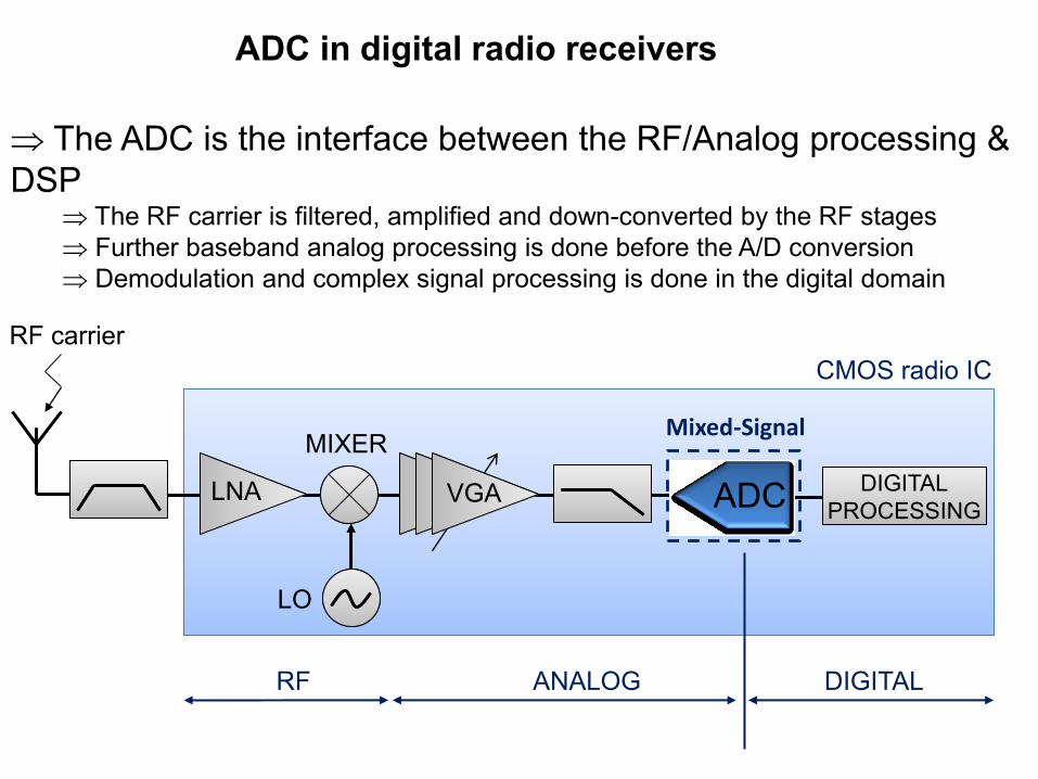
ADC in digital radio receivers
RF ANALOG DIGITAL
The ADC is the interface between the RF/Analog processing &
DSP The RF carrier is filtered, amplified and down-converted by the RF stages
Further baseband analog processing is done before the A/D conversion
Demodulation and complex signal processing is done in the digital domain
DIGITAL
PROCESSING
DIGITAL
PROCESSING VGA ADC
LO
MIXER
LNA
RF carrier
Mixed-Signal
CMOS radio IC

Problematic of RF/Analog processing in Rx Area of Analog/RF blocks do not scale as fast as digital gates
Passive components (capacitors, resistors, inductors) consumes a large area
Must be redesigned for each CMOS node : increased risks & time-to-market
QUALCOMM ATHEROS
L. Nathawad et al., ISSCC 2006
ADC in digital radio receivers
RF/Analog
~30% chip area
RF/Analog
~31% chip area
MARVELL SEMICONDUCTOR
A. Shirvani et al., CICC 2006
MEDIATEK
J-W. Lay et al., ASSCC 2008
RF/Analog
~42% chip area
Example : scaling of a 802.11 a/b/g SoC
180nm CMOS 90nm CMOS 130nm CMOS

Why do we need analog conditioning before the ADC:
ADC in digital radio receivers
ANALOG CONDITIONING
DIGITAL
PROCESSING
DIGITAL
PROCESSING VGA ADC
LO
MIXER
LNA
RF carrier

Without filtering
- Potential aliasing into signal
- Saturation of the Rx chain
Why do we need analog conditioning before the ADC: the wanted signal is often received in the presence of strong interferers
the received power can be much higher than the ADC Full-Scale
Weak signal
ADC in digital radio receivers
Strong
signal ADC
Full-Scale
Without VGA
- Saturation of the ADC
- Low SNR when the signal is weak
Strong interferers
f
f ADC
Full-Scale
f
Case 1
weak
signal
Case 2
Case 3

Why do we need analog conditioning before the ADC: the wanted signal is often received in the presence of strong interferers
the received power can be much higher than the ADC Full-Scale
Weak signal
ADC in digital radio receivers
Filter and VGA in front of the ADC Robust and High-dynamic range Rx
VGA tracks the optimal SNR
Area & Power consuming
VGA
f>0
ADC
Full-Scale
f
Case 1 Case 2 & 3
AAF

ADC in digital radio receivers
What not digitizing at antenna ?
VGA
LO
MIXER
LNA
Ideal-ADC characteristics
- Bandpass shaping
- Robust to interferers
- Very fast
DIGITAL
PROCESSING
DIGITAL
PROCESSING ADC
ADC DIGITAL
PROCESSING
DIGITAL
PROCESSING
Bandpass DS +
advanced CMOS process
- Very high dynamic range
- Low Power How much ???

ADC in digital radio receivers
What not digitizing at antenna ?
Design case: computation of the Dynamic Range (DRADC) required at the antenna
for a GSM-compliant mobile handset (800-900MHz band)
DIGITAL
PROCESSING
DIGITAL
PROCESSING ADC
Estimation of the ADC power consumption: PowerADC=FoMxfsamplingx2ENOB
fsampling=1.8GHz
FOM =50fJ/conversion-step (state-of-the-art ADC [ISSCC 2012])
PowerADC=1.6W !
State-of-the-art GSM Rx power~100mW [ISSCC 2011]
Not realistic for portable handsets, but for a non-mobile platform…
Sensitivity
@antenna
Max Power
@antenna
-102dBm
-15dBm
DRADC=87dB

Architectural trend in low-power low-cost mobile application
ADC in digital radio receivers
VGA
LO
MIXER
LNA DIGITAL
PROCESSING
DIGITAL
PROCESSING ADC
LO
MIXER
LNA DIGITAL
PROCESSING
DIGITAL
PROCESSING ADC
Baseband-ADC
High dynamic range to digitize
wanted signal+interferers
Channel selection is done in the digital domain
Increase the DR of the ADC is less expensive than increase the order of the
filtering
However an AAF must be used : CT DS ADC are good candidate !

VGA N
Improvements
IIP3 ↑ 10dB
FOM ↓ 33%
Area ↓ 22%
ADC CORE
+ 2nde order AAF
+VGA (0-18dB)
AAF ADC
CORE
N
Chip micrograph (0.13µm CMOS)
State-of-the-art A 5mW CT DS ADC with Embedded 2nd-Order Active Filter and VGA
Achieving 82dB DR in 2MHz BW”, R. Rajan, S. Pavan [ISSCC 2014]
Gain=0-18dB 2nde order
ADC in digital radio receivers

State-of-the-art “A DC-to-1GHz Tunable RF DS ADC Achieving DR = 74dB and BW = 150MHz
At f0=450MHz Using 550mW, H. Shibata et al., Analog Devices [ISSCC 2012]
ADC in digital radio receivers
VGA
LO
MIXER
LNA
Tunable blocker-tolerant bandpass ADC
with integrated LNA and variable gain
f0=300-3000 MHz
BW~100MHz
ADC DIGITAL
PROCESSING
DIGITAL
PROCESSING
DIGITAL
PROCESSING
DIGITAL
PROCESSING ADC

State-of-the-art “A DC-to-1GHz Tunable RF DS ADC Achieving DR = 74dB and BW = 150MHz
At f0=450MHz Using 550mW, H. Shibata et al., Analog Devices [ISSCC 2012]
Chip micrograph (65nm CMOS)
ADC in digital radio receivers
- fc =0-1GHz
- BW =35-100MHz
- DR =69-80dB
- Filtering=3rd-6th order
- Power =550-750mW
- Area =5.5mm²
Area is acceptable for integration in a SoC for mobile application, but the
power consumption is too high
Performances Summary
ADC

Time-Interleaved ADC
Concept : Introduced by W. C. Black and D. A. Hodges, “Time-interleaved converter arrays,
[JSSC 1980]
M-channel are time-interleaved to increase the speed of the ADC by a factor M
while the speed of each individual channel is fixed
Mxfs
M
U
X
ADC 1
ADC 2
ADC M
fs
fs
fs
F1
F2
FM
F1
F2 FM
F1
ts=1/fs
F1
F2 FM
F1
time
ts=1/fs
M samples
X(n)
X(t)

Power consumption : single-channel vs TI channels
Time-Interleaved ADC
F1
ADC
fs
ADC 1
fs/M
ADC 2
ADC M
F2
FM
F1
fs_critical fs
Single-channel
interleaved
Mxfs_critical
fs
M
U
X
Specific
processing
CLOCK
GEN fs
overhead
F1 F2
FM
Power/fs
Single-channel ADC Time-Interleaved ADC

Time-Interleaved ADC
Performance limitation Mismatch between channels due to the fabrication process
Introduce spurious tones at the reconstructed output : a specific correction
procedure is needed
Example : representation of mismatch errors in a 2x Time-Interleaved ADC (M=2):
Gain
Offset
Bandwidth
Clock skew
offset1
offset2
ADC 1
ADC 2
Mxfs fs
M
U
X
fs
Specific
processing
G2
+
+
G1
BW1
BW2
F1+DF1
F2+DF2

Time-Interleaved ADC
Example with a 2-channel Time-Interleaved ADC : M=2, channel resolution=10-bit, VREF=1V
Offset value in channel 1=1mV, the second channel is free of offset
Mxfs F1
ADC 1
fs
ADC 2
M
U
X F2
M tones are created at ixfs/M, with 0 < i < M − 1, [1]
The SFDR of the ADC is severely degraded
Offset=1mV
+ SFDR =63dBc
spurious
tone @fs/2
spurious
tone @DC
fs

Two approaches for the correction of mismatch-induced errors Mixed : digital estimation and analog correction
Fully-digital : Fully-digital : digital estimation and correction
Time-Interleaved ADC
INPUT
DAC Digital
estimation
TI ADC
Digital
estimation
Digital
correction TI ADC INPUT
Robust
Compatible with CMOS scaling
May be complex
Simple
Area & power
Portability
David Camarero et. al, [2] Han Le Duc et. al, [3]

Time-Interleaved ADC
Which architecture is best suited to TI channels ?
ADC 1
ADC 2
DSP M
U
X
what architecture ?
FLASH SAR PIPELINE DS
A few analog components
Power efficient
Area efficient
Robust
Slow

Time-Interleaved ADC
Which architecture is best suited to TI ADC ?
Single-channel CMOS ADCs presented at ISSCC/VLSI 1997-2014
≤ 11-bit
≤ 11-bit

12-bit 80-MSPS
PIPELINE ADC
12-bit 80-MSPS
SAR ADC
to 28nm CMOS
State-of-the-art
Synopsys new ADC IP generation in 28nm CMOS:
Time-Interleaved ADC
Power ↓x3
Area ↓x6
IP : 4-channel Time-Interleaved
12-bit 4x80-MSPS SAR ADC

State-of-the-art
“A 1.62GS/s Time-Interleaved SAR ADC with Digital Background Mismatch
Calibration Achieving Interleaving Spurs Below 70dBFS”,
Nicolas Le Dortz et al., ST Microelectronics & Supelec, [ISSCC 2014]
Time-Interleaved ADC
Chip micrograph (40nm CMOS)
Applications : broadband satellite, cable TVs, SDR
ISSCC’13
[1]
ISSCC’13
[2]
ISSCC’14
THIS WORK
Correction type digital
CMOS node 65nm 65nm 40nm
Speed [GS/s] 3.6 2.6 1.6
ENOB [bit] 7.5 7.8 7.6
Mismatch tones [dBFS] 50 55 70
Power [mW] 667 480 93
FOM [fJ/conv.-step] 1207 801 283
Area [mm²] 7.4 5.1 0.83
Digital part
- Area = 53%
- Power= 40%

Time-Interleaved ADC
State-of-the-art
“A 90GS/s 8b 667mW 64× Interleaved SAR ADC in 32nm Digital SOI CMOS”,
Lukas Kull et al., IBM Research & EPFL, [ISSCC 2014]
Application : optical communication
Chip micrograph (32nm CMOS SOI)
Process 32nm CMOS SOI
Supply 1.2V
Input range 0.8Vpp-diff
Speed 90 GS/s
ENOB ~5-bit
Power 667mW
FOM 203fJ/conv.-step
Area 0.45mm²