Embed Size (px)
Citation preview

ISSN (Online) : 2319 - 8753 ISSN (Print) : 2347 - 6710
International Journal of Innovative Research in Science, Engineering and Technology
Volume 3, Special Issue 3, March 2014
2014 International Conference on Innovations in Engineering and Technology (ICIET’14)
On 21st&22ndMarch Organized by
K.L.N. College of Engineering, Madurai, Tamil Nadu, India
Copyright to IJIRSET www.ijirset.com 79
M.R. Thansekhar and N. Balaji (Eds.): ICIET’14
ABSTRACT— Peak current mode control of a buck-
boost converter along with the load and transient analysis
using a PIC microcontroller is done. The new elucidation
includes a discrete time controller using digital slope
compensation technique which removes all the sub-
harmonic oscillations using a discrete staircase ramp.
Combining a digital controller with peak current control
gives a number of benefits which is implemented by a
new single chip solution with on chip comparators
without any external analog ICs. Digital slope
compensation is implemented within the PIC controller as
a digital staircase ramp using the on board modules.
KEYWORDS— DC–DC switch mode power supplies
(SMPS), peak current mode control, digital slope
compensation, transient analysis and load variation.
I. INTRODUCTION
Voltage mode control and current mode control are the
two most popular control methods used in DC-DC
converters. For controlling switched mode power
supplies, current mode control is the commonly used
method because of its advantageous features like better
dynamic performance and natural protection from short
circuit. This method can again be classified into average
and peak current mode control. A control reference is
used to regulate the peak current in peak current mode
control which has benefits likeimproved load line
regulation, better flux balancing, inherent cycle by cycle
current limiting and protection. This control is commonly
used in converters operating in continuous conduction
mode. Here, when the duty cycle becomes more than 0.5,
the feedback loop becomes highly unstable and this
instability is called as sub harmonic oscillations. By using
slope compensation technique an external ramp is added
to reduce this oscillation.
In continuous conduction mode, the current will flow
continuously throughout the switching period and one of
its advantages over discontinuous conduction mode is that
the dc conversion ratio is independent of the load, making
the analysis simpler. Also peak currents are higher in
discontinuous conduction mode which leads to heavy
losses in the path of conduction affecting the efficiency
and leading to switching stresses with higher ripples. A
switched mode power supply (SMPS) is an electronic
power supply that includes a switching regulator that
converts electric power skillfully and this high efficiency
is one of its important benefits. Source to load power flow
is the main application of SMPS; (for eg: from the main
power supply to any household appliance). During this
transfer voltage and current characteristics are adjusted
frequently. SMPS dissipates no energy when it is ideal
and is the best alternative for linear regulator that controls
the output voltage by dropping power frequently in the
pass transistor because it reduces the unwanted wastage of
energy and is highly efficient and is adaptive to usage
when smaller size and lighter weights are considered.
Peak current mode control is mainly required in
order to save the devices from damaging. In this control,
two rapidly changing ramp signals are compared and
thepeak current limit is said to be reached when these two
ramps are equal. The two ramp signals considered are the
slope compensated reference voltage signal and sensed
output inductor current. Digital control of peak current
with the implementation of slope compensation had been
a very tedious task till recent days because of the unique
Application of Digital Slope Compensation
in Peak Current Mode Control of Buck-
Boost Converter
Nikhila N,A. Rajalakshmi
Department of EEE, Rajalakshmi Engineering College, Anna University, Thandalam, Chennai, India
Department of EEE, Rajalakshmi Engineering College, Anna University, Thandalam, Chennai, India
Application of Digital Slope Compensation in Peak Current Mode Control of Buck-Boost Converter
Copyright to IJIRSET www.ijirset.com 80
M.R. Thansekhar and N. Balaji (Eds.): ICIET’14
features of the control technique and its need for extra
support circuits which made it very expensive. But
nowadays we can see that with the arrival of digital signal
processors and microcontrollers with strong performance
graphs, use of digital architecture for control has become
very simple. Microcontrollers available today are very
cheap, easier to get hold of and are of very high accuracy.
So these are used in large number of applications that
include power systems, industrial production and supply,
rectifier supplies, medical applications etc [3].
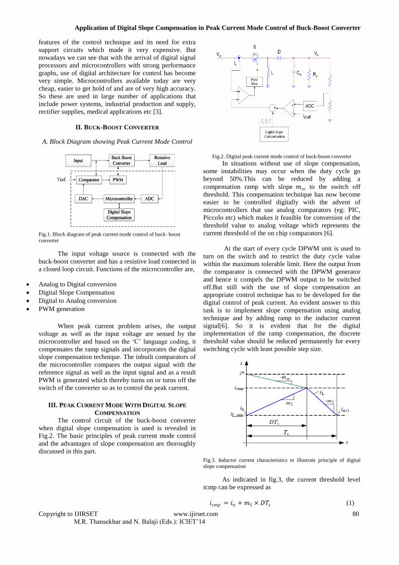
II. BUCK-BOOST CONVERTER
A. Block Diagram showing Peak Current Mode Control
Fig.1. Block diagram of peak current mode control of buck- boost
converter
The input voltage source is connected with the
buck-boost converter and has a resistive load connected in
a closed loop circuit. Functions of the microcontroller are,
Analog to Digital conversion
Digital Slope Compensation
Digital to Analog conversion
PWM generation
When peak current problem arises, the output
voltage as well as the input voltage are sensed by the
microcontroller and based on the ‘C’ language coding, it
compensates the ramp signals and incorporates the digital
slope compensation technique. The inbuilt comparators of
the microcontroller compares the output signal with the
reference signal as well as the input signal and as a result
PWM is generated which thereby turns on or turns off the
switch of the converter so as to control the peak current.
III. PEAK CURRENT MODE WITH DIGITAL SLOPE
COMPENSATION
The control circuit of the buck-boost converter
when digital slope compensation is used is revealed in
Fig.2. The basic principles of peak current mode control
and the advantages of slope compensation are thoroughly
discussed in this part.
Fig.2. Digital peak current mode control of buck-boost converter
In situations without use of slope compensation,
some instabilities may occur when the duty cycle go
beyond 50%.This can be reduced by adding a
compensation ramp with slope 𝑚𝑠𝑐 to the switch off
threshold. This compensation technique has now become
easier to be controlled digitally with the advent of
microcontrollers that use analog comparators (eg: PIC,
Piccolo etc) which makes it feasible for conversion of the
threshold value to analog voltage which represents the
current threshold of the on chip comparators [6].
At the start of every cycle DPWM unit is used to
turn on the switch and to restrict the duty cycle value
within the maximum tolerable limit. Here the output from
the comparator is connected with the DPWM generator
and hence it compels the DPWM output to be switched
off.But still with the use of slope compensation an
appropriate control technique has to be developed for the
digital control of peak current. An evident answer to this
task is to implement slope compensation using analog
technique and by adding ramp to the inductor current
signal[6]. So it is evident that for the digital
implementation of the ramp compensation, the discrete
threshold value should be reduced permanently for every
switching cycle with least possible step size.
Fig.3. Inductor current characteristics to illustrate principle of digital slope compensation
As indicated in fig.3, the current threshold level
icmp can be expressed as
𝑖𝑐𝑚𝑝 = 𝑖𝑛 + 𝑚1 × 𝐷𝑇𝑠 (1)
Application of Digital Slope Compensation in Peak Current Mode Control of Buck-Boost Converter
Copyright to IJIRSET www.ijirset.com 81
M.R. Thansekhar and N. Balaji (Eds.): ICIET’14
𝑖𝑐𝑚𝑝 = 𝑖∗ − 𝑚𝑠𝑐 × 𝐷𝑇𝑠 (2)
From (1) and (2) we get
𝐷𝑇𝑠 =𝑖∗−𝑖𝑛
𝑚1+𝑚𝑠𝑐 (3)
Using (3) to eliminate 𝐷𝑇𝑠 from (2) we get
𝑖𝑐𝑚𝑝 = 𝑖∗ − 𝑚𝑠𝑐𝑖∗−𝑖𝑛
𝑚1+𝑚𝑠𝑐 (4)
Now a compensating factor 𝑘𝑠𝑐 is introduced which is,
𝑘𝑠𝑐 =𝑚𝑠𝑐
𝑚1 (5)
Thus (4) can be expressed as
𝑖𝑐𝑚𝑝 = 𝑖∗ −𝑘𝑠𝑐
1+𝑘𝑠𝑐 𝑖∗ − 𝑖𝑛 (6)
So the threshold value of the comparator current
can be measured by considering the reference value 𝑖∗ which we get from the voltage controller and this is now
transferred to the digital control through the analog to
digital converter (ADC). Choosing of the compensating
factor should be appropriate in order to adjust the
obtained current threshold value with the slope
compensation technique used [6].
IV.DESIGN EXAMPLE
A. Calculation Of Duty Cycle
After choosing the various parameters of the
converter the next priority objective is to obtain the duty
cycle for the buck mode which is minimum and for the
boost mode which is maxima [10].
𝐷𝑏𝑢𝑐𝑘 =𝑉0 × ɳ
𝑉𝑠𝑚𝑎𝑥
(7)
𝐷𝑏𝑜𝑜𝑠𝑡 = 1 −𝑉𝑠𝑚𝑖𝑛 × ɳ
𝑉0
(8)
Where ɳ is the estimated efficiency.
B. Inductor Selection
We know that as the inductance value increases
the higher is the maximum output current that is plausible
since the ripple currentlessens[10].
In the buck mode the inductor value can be
calculated properly and correctly calculated using the
equation:
𝐿 >𝑉𝑜×(𝑉𝑠 𝑚𝑎𝑥 −𝑉𝑜 )
𝑘𝑖𝑛𝑑 ×𝐹𝑠𝑤 ×𝑉𝑠 𝑚𝑎𝑥 ×𝐼𝑜 (9)
Similarly in the boost modethe following
equation is a fine [10] estimate for the appropriate
inductance value:
𝐿 >𝑉𝑠 𝑚𝑖𝑛
2 ×(𝑉𝑜−𝑉𝑠 𝑚𝑖𝑛 )
𝑓𝑠×𝑘𝑖𝑛𝑑 ×𝐼𝑜×𝑉𝑜2 (10)
When the ripple current shown in the inductor is
20or 40 percentage of the output current it is noted to be a
proper calculation.
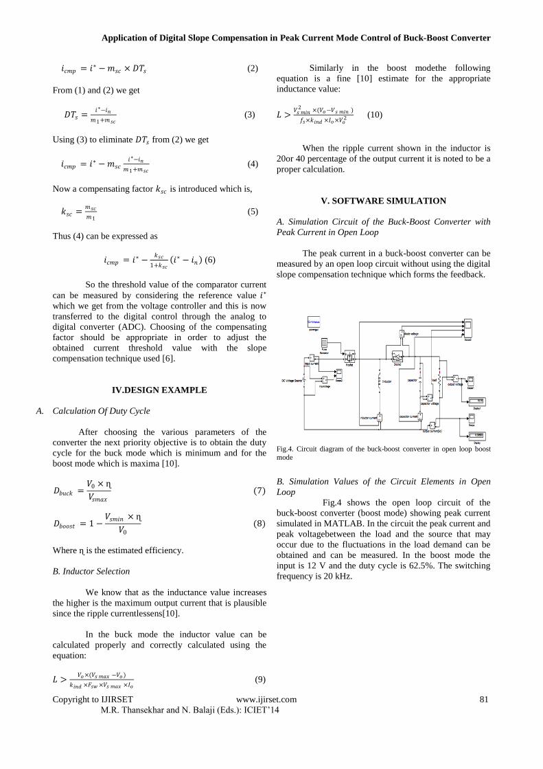
V. SOFTWARE SIMULATION
A. Simulation Circuit of the Buck-Boost Converter with
Peak Current in Open Loop
The peak current in a buck-boost converter can be
measured by an open loop circuit without using the digital
slope compensation technique which forms the feedback.
Fig.4. Circuit diagram of the buck-boost converter in open loop boost
mode
B. Simulation Values of the Circuit Elements in Open
Loop
Fig.4 shows the open loop circuit of the
buck-boost converter (boost mode) showing peak current
simulated in MATLAB. In the circuit the peak current and
peak voltagebetween the load and the source that may
occur due to the fluctuations in the load demand can be
obtained and can be measured. In the boost mode the
input is 12 V and the duty cycle is 62.5%. The switching
frequency is 20 kHz.
Application of Digital Slope Compensation in Peak Current Mode Control of Buck-Boost Converter
Copyright to IJIRSET www.ijirset.com 82
M.R. Thansekhar and N. Balaji (Eds.): ICIET’14
Table.I shows the specifications of the buck-boost
converter in open loop circuit. Using these values the
simulation has been done and the waveforms are
analyzed.
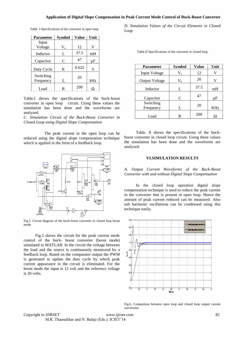
C. Simulation Circuit of the Buck-Boost Converter in
Closed Loop using Digital Slope Compensation
The peak current in the open loop can be
reduced using the digital slope compensation technique
which is applied in the form of a feedback loop.
Fig.5. Circuit diagram of the buck-boost converter in closed loop boost
mode
Fig.5 shows the circuit for the peak current mode
control of the buck- boost converter (boost mode)
simulated in MATLAB. In the circuit the voltage between
the load and the source is continuously monitored by a
feedback loop. Based on the comparator output the PWM
is generated to update the duty cycle by which peak
current appearance in the circuit is eliminated. For the
boost mode the input is 12 volt and the reference voltage
is 20 volts.
D. Simulation Values of the Circuit Elements in Closed
Loop
Table.II Specifications of the converter in closed loop
Table. II shows the specifications of the buck-
boost converter in closed loop circuit. Using these values
the simulation has been done and the waveforms are
analyzed.
VI.SIMULATION RESULTS
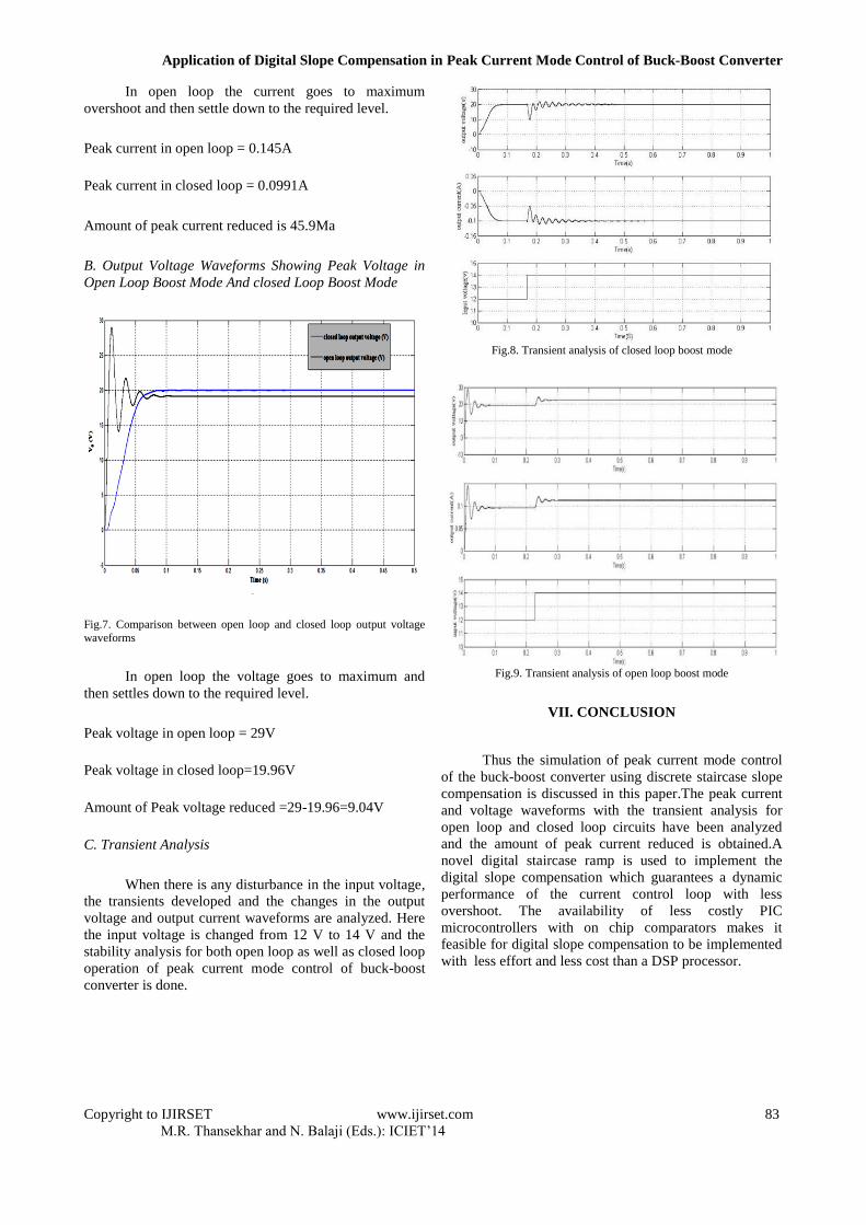
A. Output Current Waveforms of the Buck-Boost
Converter with and without Digital Slope Compensation
In the closed loop operation digital slope
compensation technique is used to reduce the peak current
in the converter that is present in open loop. Hence the
amount of peak current reduced can be measured. Also
sub harmonic oscillations can be condensed using this
technique easily.
Fig.6. Comparison between open loop and closed loop output current
waveforms
Parameter Symbol Value Unit
Input
Voltage Vs 12 V
Inductor L 37.5 mH
Capacitor C 47 µF
Duty Cycle K 0.625 S
Switching
Frequency fs 20
kHz
Load R 200 Ω
Parameter Symbol Value Unit
Input Voltage Vs 12 V
Output Voltage V0 20 V
Inductor L 37.5 mH
Capacitor C 47
µF
Switching
Frequency fs 20
KHz
Load R 200 Ω
Table. I Specifications of the converter in open loop
Application of Digital Slope Compensation in Peak Current Mode Control of Buck-Boost Converter
Copyright to IJIRSET www.ijirset.com 83
M.R. Thansekhar and N. Balaji (Eds.): ICIET’14
In open loop the current goes to maximum
overshoot and then settle down to the required level.
Peak current in open loop = 0.145A
Peak current in closed loop = 0.0991A
Amount of peak current reduced is 45.9Ma
B. Output Voltage Waveforms Showing Peak Voltage in
Open Loop Boost Mode And closed Loop Boost Mode
Fig.7. Comparison between open loop and closed loop output voltage
waveforms
In open loop the voltage goes to maximum and
then settles down to the required level.
Peak voltage in open loop = 29V
Peak voltage in closed loop=19.96V
Amount of Peak voltage reduced =29-19.96=9.04V
C. Transient Analysis
When there is any disturbance in the input voltage,
the transients developed and the changes in the output
voltage and output current waveforms are analyzed. Here
the input voltage is changed from 12 V to 14 V and the
stability analysis for both open loop as well as closed loop
operation of peak current mode control of buck-boost
converter is done.
Fig.8. Transient analysis of closed loop boost mode
Fig.9. Transient analysis of open loop boost mode
VII. CONCLUSION
Thus the simulation of peak current mode control
of the buck-boost converter using discrete staircase slope
compensation is discussed in this paper.The peak current
and voltage waveforms with the transient analysis for
open loop and closed loop circuits have been analyzed
and the amount of peak current reduced is obtained.A
novel digital staircase ramp is used to implement the
digital slope compensation which guarantees a dynamic
performance of the current control loop with less
overshoot. The availability of less costly PIC
microcontrollers with on chip comparators makes it
feasible for digital slope compensation to be implemented
with less effort and less cost than a DSP processor.

Application of Digital Slope Compensation in Peak Current Mode Control of Buck-Boost Converter
Copyright to IJIRSET www.ijirset.com 84
M.R. Thansekhar and N. Balaji (Eds.): ICIET’14
ACKNOWLEDGMENT
The authors wish to acknowledge the
management of Rajalakshmi Engineering College and
especially the faculties of EEE department for their full
support during the course of this project phase. Also
gratefully thank the helpful comments and suggestions of
the reviewers which have greatly improved the
presentation.
REFERENCES [1 ]Brad Bryant and Marian Kazimierczuk, k. (2005) ‘Modellingthe
Closed-Current Loop of PWM Boost DC–DC ConvertersOperating in CCM With Peak Current-Mode Control’, IEEE Transactions on
circuits and systems—I: regular papers, vol 52, no.11
[2] Brad Bryant and Marian Kazimierczuk, k. (2005) ‘Open- Loop Power-Stage Transfer Functions Relevant to Current-Mode
Control of Boost PWM Converter Operating in CCM’, IEEE
Transactions on Circuits and Systems—I: regular papers, vol 52,no.10 [3]
[3]Brett Novak (2012) ‘Implementing peak current mode control of a
switch mode power supply with a single microcontroller’, Texas
Instrument
[4] [4] Everrert Rogers (2002) ‘Understanding Buck-Boost Power Stages in Switch Mode Power Supplies’, Application Report
SLVA059A
[5] GiridharanShanmugavel( 2012)‘Using a Peak-Current-Mode Controller to Design aBoost Converter’, Application Note 5503
[6] Grote, T. ,Schafmeister, F. , Figge1, H. , Fröhleke1, N. and Ide,
P. (2004) ‘Adaptive Digital Slope Compensation for Peak Current Mode’, University of Paderborn, Power Electronics and Electric
Drives, Germany
[7] Hyoung Cho, Y. and Enrico Santi (2009) ‘ Peak Current Mode-Controlled Buck Converter with Positive Feed forward Control’,
University of South Carolina
[8] Jian Li and Fred Lee, C. (2010) ‘New Modelling Approach and Equivalent Circuit Representation for Current-Mode
Control’, IEEE Transactions on Power Electronics, vol 25,no.5
[9] Jian Li (1990) ‘Current Mode Control: Modeling and its Digital Application’, Dissertation submitted to Virginia Polytechnic
Institute and State University
[10] Michael Green (2012) ‘Design Calculations for Buck-Boost
Converters’, Application Report SLVA535A
[11] Ray Ridley (2001) ‘A More Accurate Current Mode Control
Model’, Ridley Engineering Inc. [12] SouvikChattopadhyay and Somshubhra Das (2006) ‘ A
Digital Current-Mode Control Technique for DC–DC
Converters’, IEEE Transactions on Power Electronics, vol 21, no.6
[13] Ting Qian (2013) ‘Subharmonic Analysis for Buck Converters
with Constant On-Time Control and Ramp Compensation’, IEEE Transactions on Industrial Electronics, vo 60, no4
[14] Robert Sheehan (2007) ‘Understanding and Applying Current-
Mode Control Theory’, Practical Design Guide For Fixed-Frequency, Continuous Conduction-Mode Operation
[15] RichardPoley and Ali Shirsavar (2012) ‘Digital Peak Current
Mode Control With Slope Compensation Using the TMS320F2803x’,Application Report SPRABE7A