Embed Size (px)
Citation preview

The 1st Global COE International SymposiumSatellite meeting “Recent activities of IDER units”
Y. Miura, M. Imade, H. Kakigano, Y. Kamakura, F. Kawamura, O. Saeki, H. Sugihara, R. Simanjorang, T. Ise, H. Iwamoto
Osaka University, Mitsubishi Electric Corp.
Jan. 18, 2008

IntroductionGoal of our IDER unitMembersTargets Present activitiesSummary
2

Power Electronics engineering is one of the promising solutions for problems of energy saving and CO2 reduction.Motor drivesPower systemsDistributed generations
High efficiency, High performance
3

Higher efficiency, lower volume→ Higher power density
G. Majumdar, “Power Modules As Key Component Group For Power Electronics,” the Proceedings of PCC 2007, Nagoya.(c) 2007 IEEE)
Limit of Si based device
• GaN• SiC
Shift to next generation devices
4

Higher voltageHigher frequency smaller L and CHigher operating temperatureLower losses smaller cooling componentsConducting lossesSwitching losses
Bandgap(eV)
Breakdownstrength(MV/cm)
Electronmobility(cm2/Vs)
Electronsaturationvelocity(x107cm/s)
Thermalconductivity(W/cm deg)
GaN 3.43 3.0 1200 2.7 1.3SiC 3.26 2.8 1000 2 4.9Si 1.12 0.3 1350 1 1.51
Higher power density
5

Establishment of the concept of GaN devices for power electronics applications
Driving force for development and application of GaN devices
“Application‐driven” development6

Name Specialty areaYushi Miura Power Electronics (PE) Engineering, Unit LeaderMamoru Imade GaN crystallizationHiroaki Kakigano PE Engineering, Distributed GenerationsYoshinari Kamakura Device simulationFumio Kawamura GaN crystallizationOsamu Saeki Optimization AnalysisHideharu Sugihara Optimization AnalysisRejeki Simanjorang PE Engineering, Switching power suppliesToshifumi Ise PE Engineering, Unit AdvisorHideo Iwamoto Power Device Application, Unit Advisor
7

1. Market research and Evaluation of required performance of next generation devices
Feedback to crystallization engineering
2. Literature research and construction knowledge database
3. Prediction of device performances and development of device design methodology
Device simulation and optimization technique
4. Establishment of implementation technology8
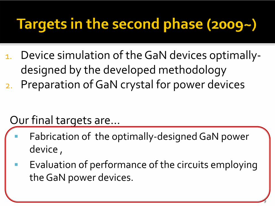
1. Device simulation of the GaN devices optimally‐designed by the developed methodology
2. Preparation of GaN crystal for power devices
Our final targets are…Fabrication of the optimally‐designed GaN power device ,Evaluation of performance of the circuits employing the GaN power devices.
9

Literature research and construction of the knowledge base on the Web.Evaluation of performance of the next generation power devices at present.Dynamic performance of passive circuit components such as inductors, capacitors, and resistors will be also investigated.
10

For Knowledge management, knowledge base has been constructed on the Web using Blog technology.
Literature informationTechnical intelligenceSeminar and lecture informationActivity reports
11

Literature research and construction of the knowledge base on the Web.Evaluation of performance of the next generation power devices at present.Dynamic performance of passive circuit components such as inductors, capacitors, and resistors will be also investigated.
12

passive components
SiC devices
GaN devices performance measurement
Measurement of Dynamic characteristics
Drive circuit
Voltage and current
Test Circuit
Osc.
Probes
DSP board
◆Measurement and evaluation of performance
◆ Loss estimation◆modeling of switch devices
and passive components 13

To establish the concept for application of the GaNpower devices, our IDER unit has been organized by the experts in different engineering fields.
The device simulation method, the device design methodology and the circuit implementation technology, which will be interdisciplinary developed in this unit, will be novel tools for development and application of the power devices.
14