Embed Size (px)
Citation preview

EE130 Lecture 35, Slide 1Spring 2007
Lecture #35
OUTLINE
The MOS Capacitor: Final comments
The MOSFET:
• Structure and operation
Reading: Chapter 17.1
EE130 Lecture 35, Slide 2Spring 2007
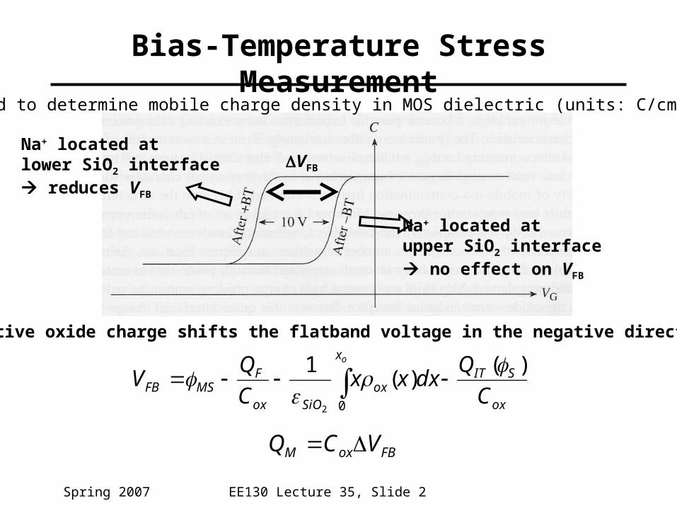
Bias-Temperature Stress Measurement
FBoxM VCQ
Na+ located at upper SiO2 interface no effect on VFB
Na+ located at lower SiO2 interface reduces VFB
VFB
ox
SIT
x
oxSiOox
FMSFB C
Qdxxx
C
QV
o )()(
1
02
Used to determine mobile charge density in MOS dielectric (units: C/cm2)
Positive oxide charge shifts the flatband voltage in the negative direction:

EE130 Lecture 35, Slide 3Spring 2007
Clarification: Effect of Interface Traps
Traps cause “sloppy” C-V and also greatly degrade mobility in channel
ox
SITG C
QV
)(
“Donor-like” traps arecharge-neutral whenfilled, positively chargedwhen empty
Positive oxide chargecauses C-V curve toshift toward left (more shift as VG decreases)
(a)
(a) (b)
(b)
(c)
(c)

EE130 Lecture 35, Slide 4Spring 2007
In 1935, a British patent was issued to Oskar Heil. A working MOSFET was not demonstrated until 1955.
Invention of the Field-Effect Transistor
EE130 Lecture 35, Slide 5Spring 2007
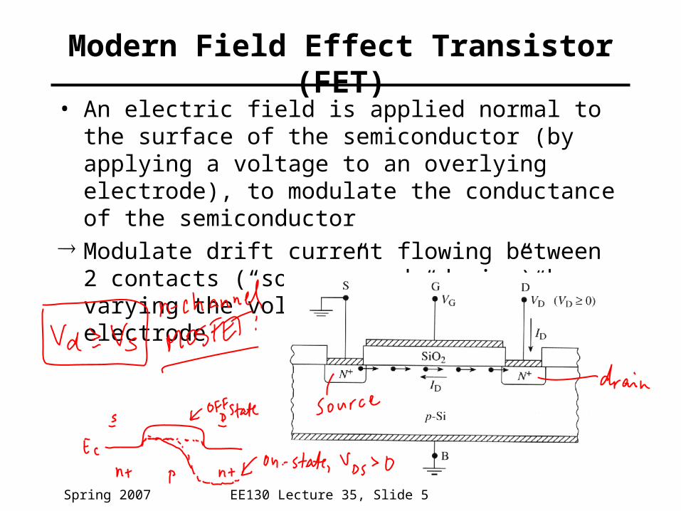
Modern Field Effect Transistor (FET)• An electric field is applied normal to the surface of the
semiconductor (by applying a voltage to an overlying electrode), to modulate the conductance of the semiconductor
Modulate drift current flowing between 2 contacts (“source” and “drain”) by varying the voltage on the “gate” electrode

EE130 Lecture 35, Slide 6Spring 2007
The Bulk-Si MOSFET
• Current flowing between the SOURCE and DRAIN is controlled by the voltage on the GATE electrode
Substrate
Gate
Source Drain
Metal-Oxide-Semiconductor Field-Effect Transistor:
GATE LENGTH, Lg
OXIDE THICKNESS, Tox
JUNCTION DEPTH, Xj
M. Bohr, Intel DeveloperForum, September 2004
Desired characteristics:• High ON current• Low OFF current
• “N-channel” & “P-channel” MOSFETs operate in a complementary manner“CMOS” = Complementary MOS |GATE VOLTAGE|
CU
RR
ENT
VT

EE130 Lecture 35, Slide 7Spring 2007
N-channel vs. P-channel
• For current to flow, VGS > VT
• Enhancement mode: VT > 0
• Depletion mode: VT < 0
– Transistor is ON when VG=0V
P-type Si
N+ poly-Si
n-type Si
P+ poly-Si
NMOS PMOS
N+ N+ P+ P+
• For current to flow, VGS < VT
• Enhancement mode: VT < 0
• Depletion mode: VT > 0
– Transistor is ON when VG=0V

EE130 Lecture 35, Slide 8Spring 2007
Enhancement Mode vs. Depletion Mode
Enhancement Mode Depletion Mode
Conduction between source and drain regions is enhanced by applying a gate voltage
A gate voltage must be appliedto deplete the channel region in order to turn off the transistor
EE130 Lecture 35, Slide 9Spring 2007
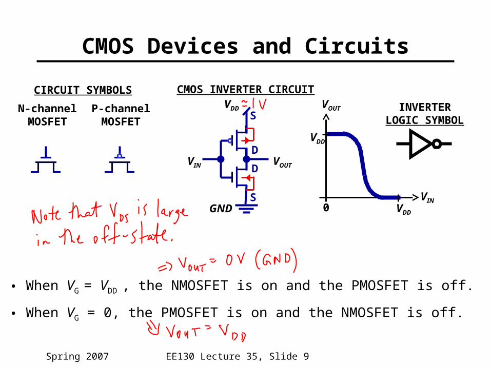
CMOS Devices and Circuits
CIRCUIT SYMBOLS
N-channelMOSFET
P-channelMOSFET
GND
VDDS
S
D
D
CMOS INVERTER CIRCUIT
VIN VOUT
VOUT
VIN0 VDD
VDD
INVERTERLOGIC SYMBOL
• When VG = VDD , the NMOSFET is on and the PMOSFET is off.
• When VG = 0, the PMOSFET is on and the NMOSFET is off.

EE130 Lecture 35, Slide 10Spring 2007
“Pull-Down” and “Pull-Up” Devices• In CMOS logic gates, NMOSFETs are used to connect the output to
GND, whereas PMOSFETs are used to connect the output to VDD.– An NMOSFET functions as a pull-down device when it is turned
on (gate voltage = VDD)– A PMOSFET functions as a pull-up device when it is turned on
(gate voltage = GND)
F(A1, A2, …, AN)
PMOSFETs only
NMOSFETs only…
…
Pull-upnetwork
Pull-downnetwork
VDD
A1
A2
AN
A1
A2
AN
input signals

EE130 Lecture 35, Slide 11Spring 2007
CMOS NAND Gate
A B F0 0 10 1 11 0 11 1 0
A
F
B
A B
VDD

EE130 Lecture 35, Slide 12Spring 2007
CMOS NOR Gate
A
F
B
A
B
VDD A B F0 0 10 1 01 0 01 1 0

EE130 Lecture 35, Slide 13Spring 2007
CMOS Pass Gate
A
X Y
A
Y = X if A