Embed Size (px)
Citation preview

Spider
Place and Route Training Part I

Spider Place and Route Training - 2 -
Day 1 Introduction to Place and Route
Overview Additional Terminology & Concepts Background
Background Channel vs. Area Place & Route
Interface Standards GDSII, LEF/DEF, Liberty .lib, verilog, SDF, SPICE,
and DSPF Design Methods
Logical vs. Physical Synthesis Methods Chips vs. Blocks Net-Length vs. Congestion Driven Methods The Clock-Tree Concept and Methods Timing-Driven vs. Non-Timing-Driven Methods Avoiding vs. Fixing Antenna and SI Issues VDSM For Beginners
Design Flow Process The Need for Frame Views and Abstraction Handling Designs with Macros Handling Large Designs (Hierarchical Methods) Power Planning 101 Handling Design Changes (ECOs) The Need for Placement Optimization Design Closure Verification and STA
Product Overview of Spider Netlist Import Management Library Data Prep Design Planning and Prototyping Placement Optimization CTS Chip Finishing and Assembly Verification RC and Timing Extraction LOAD_DESIGN SLNET GDSGDL GDLPDL Data Prep Lab1 (1hr) SDL / CDL / TDL / PDL / DDL PCOMP LIB2DDL DDLLOAD Data Prep Lab2 (1hr)

Spider Place and Route Training - 3 -
Day 2 NTPGEN TIMELOAD PGREDIT / PGROUTE GPLACE Placement Lab (1hr) CLKTREE SDLGEN / VGEN GRDGEN GAROUT REDIT / RROUTE PGRLOAD / PGRDUMP / RLOAD /
RDUMP Routing Lab (1hr)
Day 3 MASKOUT VERIFY VERCON GADELAY CAPCLC EXPERT / GUARDIAN / HIPEX-RC ACCUCORE STA Design Strategies and Workarounds Tapeout Final (Lab) 4hrs
Day 4 (AEs ONLY) Design Strategies and Workarounds

Spider
Introduction to Place and Route
- 4 -

Introduction to Place and Route
Overview
- 5 -

Spider Place and Route Training
This section is intended to provide an introduction to the evolution and explanation of the main concepts and issues associated with place and route based design flows and the placement and routing process
For additional details on specific features of specific design tools or training guidance, please see the respective training manuals for each tool including their “intro” and “quickstart” guides
A “boot camp” on details of the Silvaco Spider place and route design flow follows this section
- 6 -

Introduction to Place and Route
Additional Terminology and Concepts
- 7 -

Spider Place and Route Training
Register Transfer Level (RTL) – Typical verilog syntax used to describe the functionality of a design in high level constructs, which must be synthesized into a gate level netlist in the target cell library technology
Scan insertion – Design-For-Test (DFT) method where registers (latches/flip-flops) in the design are converted to “muxed” versions that directly interconnect through special paths “chains” to permit loading and reading the stored state of a chip in a special test mode to check for manufacturing defects
Regression simulation(analysis) – Vector based method of validating that RTL and a gate-level netlist match in behavior
Formal verification – Vector-less method of mathematically validating that RTL and a gate-level netlist match in behavior
Static Timing Analysis(STA) – Vector-less method of validating the timing characteristics of a design based on cell function and pre-characterized timing characteristics and netlist connectivity
“Doubleback” rows – Two standard cell placement row regions, which abut or overlap sharing a common power rail (“head-to-head” or “tail-to-tail” or both).
Dummy metal fill – Additional geometry to assure small features manufacture as defined in the chip layout
Antenna effect – Destructive effect during manufacturing due to static buildup
- 8 -

Introduction to Place and Route
Background
- 9 -

Spider Place and Route Training
Chip design originated with the use of “full-custom” transistor-level layout. But as design size and complexity grew, automated layout (and design) methods became a necessity
The use of predefined functions and cell layouts eased the design burden permitting “design-reuse” of logic gate library primitives
To keep the number of cells in the library reasonable, a standard set of functions and drive strengths were defined that were most commonly required and could be easily described with a basic logical function to permit easy construction of random logic
Verilog Register Transfer Level(RTL) was much faster to simulate than a gate level structural verilog netlist but required that the chip be designed twice: once at the RTL level and once at the gate level. The two were then compared by regression simulation to assure equivalence. RTL, however, is a functional only check, whereas the regression simulation could also include gate-level timing
To address timing verification, SDF timing data was backannotated into the gate level netlist in the regression simulations, but this slowed down simulation significantly
- 10 -

Spider Place and Route Training
Large and complex clock networks resulted requiring Clock-Tree-Synthesis (CTS) to handle idealized clock nets that required detailed placement information to be addressed adequately
Automation caught up with the logic design process and logic synthesis took over the gate level design process with a subset of the simulation language, which became a functional description Hardware Description Language (HDL)
Logic synthesis could translate RTL into a gate level netlist using the target library technology and meet a defined timing requirement to the extent that the RTL structure and the library timing characteristics were able to do
To assure that the “golden” simulated RTL and the synthesized gate level netlist behaved as intended regression, simulation continued to be used. To address the slow simulations, however, STA methods took over timing verification in most situations
As chips grew, post-manufacture testing became problematic and resulted in “scan” based methods to permit easy and automated design and testing, but at the cost of increased die size to fit the larger circuitry it required to implement
Automated Test Pattern Generation (ATPG) developed to address the complexity of designing the massive vector sets required
- 11 -

Spider Place and Route Training
Automation again caught up and mathematical based “proof” methods using formal verification took over the need for regression simulations in most situations
Logic synthesis was replaced by physical synthesis, which merged placement into the logic design process improving timing convergence
Initially, physical synthesis capacities lagged significantly behind that of logic synthesis because of additional data management and processing complexity. But, advanced algorithms and data management methods largely resolved most of the limitations
To address the need to exchange physical synthesis results with backend tools, LEF/DEF instead of verilog and GDSII (or LEF) became the interface method. This adds placement (and floorplanning) details
Hierarchical design methods with advanced floorplanning features were developed into the backend tools to address data management limitations due to the ever increasing chip gate counts that advanced technologies could provide
Throughout all this, backend tools continuously adapted to the ever constant changing design and interface requirements of the design process
- 12 -

Spider Place and Route Training
Not only were the front-end methods and interfaces changing, also additional backend design requirement were added to address an ever new and increasing set of design problems
Advanced technologies required new and complex layout design rules and changes in physical library design methods and formats (LEF/DEF were constantly being updated)
Additional data “views” of cell characteristics and process modeling required inclusion to enable design closure in the backend
Detailed obstruction modeling, timing, antenna effects, functional behavior, test features, power and EM characteristics, noise modeling, and other design details became part of the data to handle and was required to achieve design closure on large and complex designs
Backend place and route tools no longer had the “simple” job of just placing and routing the design but instead became “design closure” tools
Features like Power Network Analysis (PNA) and Power Network Synthesis (PNS) were added to aid and automate the design of ever increasing complex PWR and GND sizing and routing, power pad insertion and placement optimization, IR drop and EM analysis as power densities climbed and chip size (not just gate count) grew
- 13 -

Spider Place and Route Training
Hierarchical design planning and prototyping became requirements to address the size and complexity of state-of-the-art chips requiring features like “on-the-fly” quick synthesis and area estimation and handling incomplete netlists and multi-view physicals of macros
Netlist management to address difference and changes between the logic and the physical partitioning and large netlist change updates (not just 1-2% ECOs) became necessary
Re-sizing and re-structuring of the original design netlist to address timing errors became an increasing challenge and requirement, not just on a local level but also on a global chip level
Detailed timing estimation and extraction requirements increased as wire delays and loading forced backend tools to integrate STA timing engines and RC extraction details into the place and route design problem to aid design closure
Noise and SI effects due to routing (and logic design/placement interactions) required fast and detailed RC estimation and extraction capabilities to avoid and fix physical and logical-physical interaction problems due to parasitic coupling effects
- 14 -

Spider Place and Route Training
VDSM brought new challenges including variable design rules based on line and via density since what was designed in layout and what was manufactured for the masks and the chip became increasingly abstract due to significant post-layout “proximity” correction between the delivered GDSII and the generated masks. Design-For-Manufacture (DFM) and Design-For-Yield (DFY) became realities that place and route tools needed to address as process and lithographic variability moved from the FAB process and into the design process
The result of all these issues has driven what was mostly a three step design process (front-end, backend, and FAB) into one step, requiring complex, integrated, cooperative, and expensive design methodology to address latest process technologies
The System-on-a-Chip (SoC) concept enabled by these latest technologies have resulted in fewer and fewer tapeouts as one chip replaces many and bifurcated place and route requirements between the “bleeding edge” and “mainstream” (0.13um and above) mixed-signal designs
Silvaco’s Spider place and route design flow system is targeted at providing the best of these advances without the expensive design flow complexity needed to support VDSM and mega-million gate chip design requirements
Designing chips should be simple and NOT require expert knowledge and huge budgets to do so
- 15 -

Spider Place and Route Training
Channel based methods are based on alternating rows of standard cells with “channels” of (typically) horizontal routing in 2-metal (or possibly 3-metal) technologies where cell wiring would otherwise restrict routing “over-the-cell”
Channels often vary in height, which is controlled by the place and route process that results in a “variable-die-size” layout
Channel based technologies often use channel based cell libraries that have poly gate extensions beyond the top or bottom or both sides of the cell since they expect a channel to be present
Area based (Fixed) methods are based on floorplans where two or more “doubleback” rows may be combined to produce a channel-less design
Since there are no channels, horizontal routing must occur over-the-cell and routing requirements must be balanced with a “fixed” number of routing “tracks”
Placement density control assures that this “track” limit does not exceed on both global and local levels
To assure this, a placement optimization step “tunes” the overall placement to eliminate “hot-spots” where local routing congestion is occurring
Unlike the channel based variable die method, which is assures route completion (but not achieving target die size), fixed die area based methods always achieve their target die size (but may not assure route completion)
- 16 -

Introduction to Place and Route
Interface Standards
- 17 -

Spider Place and Route Training
GDSII – Graphical Design System II LEF – Library Exchange Format DEF – Design Exchange Format Liberty .lib – Timing Library Format Verilog – Netlist format for gate level circuit description also a simulation
description language for RTL SDC – Synopsys Design Constraints SDF – Standard Delay Format, gate level timing SPICE – Netlist format for LVS and transistor circuit description DSPF – Detailed Standard Parasitic Format, R & C wiring effects
- 18 -

Spider Place and Route Training
Contains physical description data of objects Contains placement location (and orientation) data SREFs of instances of objects Netlist information (connectivity) is not part of the standard PATHS define wires, have layers, width and joint and end-style attributes, and are defined by
vertex coordinates (they are the majority of the design data) BOUNDARIES (polygons) define most other data structures. (Boxes are a special case sub-
structure in most layout tools, but are not part of the GDSII standard) A manufacturing grid is defined (but not enforced). Objects should remain “on-grid” to avoid
manufacturing differences with the GDSII The manufacturing grid is different from the routing grid Layers range from 0-63 (optionally 0-255) Data-types (per layer) range from 0-63, giving a total “layer count” of 256 *?"|:;,.\/=<>() are illegal in cell names Cell names limited to '1' - '9', 'A' - 'Z', '_' and '$‘ are recommended and should be unique
within the first 20 chars for maximum compatibility Hierarchy and arrays of objects (instances) are permitted but recursion is not A technology file, which defines graphical and layer use details for a given technology and
design, must often accompany GDSII data for correct interpretation
- 19 -

Spider Place and Route Training - 20 -
2K chars / line distance in microns TECHNOLOGY LEF defines:
measurement method manufacturing grid unit scale factors default and nondefault
via construction & Rvalue Layer (cut & routing)
width, spacing antenna rules basic RC & EM properties
LIBRARY LEF defines: via definition site details
Class (pad,core) symmetry(x, y, r90) rowpattern size
MACRO class(core,block,pad,core), type, and
equivalent cells origin, offset, symmetry, site, size, and
density (per layer) pin details (name, direction, taper, use,
shape, layers (width, paths, rectangles, polygons, vias), and antenna details)
obstruction details (layers (overlap, width, spacing, paths, rectangles, polygons, vias))

Spider Place and Route Training - 21 -
[‘VERSION’ <number>‘;’] [‘BUSBITCHARS’ ‘“’<delimiterPair>‘”’‘;’] [‘DIVIDERCHAR’ ‘“’<character>‘”’‘;’] [<UNITS_statement>] [‘MANUFACTURINGGRID’ <value>‘;’] [‘USEMINSPACING’ ‘OBS’ {‘ON’|‘OFF’}‘;’] [‘CLEARANCEMEASURE’ {‘MAXXY’|‘EUCLIDEAN’}‘;’] [<PROPERTYDEFINITIONS_statement>] [<LAYER_(Nonrouting)_statement> | <LAYER_(Routing)_statement>]… [<SPACING_statement>] [‘MAXVIASTACK’ <value> [‘RANGE’ <bottomLayer> <topLayer>]‘;’] [<VIA_statement>]… [<VIARULE_statement>]… [<VIARULE_GENERATE_statement>]… [<NONDEFAULTRULE_statement>]… [<SITE_statement>]… [‘BEGINEXT’ ‘“’<tag>‘”’ <extension> ‘ENDEXT’]… [‘END LIBRARY’]

Spider Place and Route Training - 22 -
<UNITS_statement> ::= ‘UNITS’ [‘TIME’‘NANOSECONDS’ <convertFactor>‘;’] [‘CAPACITANCE’ ‘PICOFARADS’ <convertFactor>‘;’] [‘RESISTANCE’ ‘OHMS’ <convertFactor>‘;’] [‘POWER’ ‘MILLIWATTS’ <convertFactor>‘;’] [‘CURRENT’ ‘MILLIAMPS’ <convertFactor>‘;’] [‘VOLTAGE’ ‘VOLTS’ <convertFactor>‘;’] [‘DATABASE’ ‘MICRONS’ <LEFconvertFactor>‘;’] [‘FREQUENCY’ ‘MEGAHERTZ’ <convertFactor>‘;’] ‘END UNITS’ <PROPERTYDEFINITIONS_statement> ::= ‘PROPERTYDEFINITIONS’ [<objectType> <propName> <propType> [‘RANGE’ <min> <max>] [<value> | ‘“’<stringValue>‘”’]‘;’]… ‘END PROPERTYDEFINITIONS’

Spider Place and Route Training - 23 -
<LAYER_cut_statement> ::= [{‘LAYER’ <layerName> ‘TYPE’ ‘CUT’‘;’ [‘SPACING’ <minSpacing> [{‘LAYER’ <2ndLayerName>} | {‘ADJACENTCUTS’ {‘3’|‘4’} ‘WITHIN’ <distance>} | ‘CENTERTOCENTER]‘;’]… [‘WIDTH’ <minWidth>‘;’] [‘ENCLOSURE’ [‘ABOVE’|‘BELOW’] <overhang1> <overhang2> [WIDTH <minWidth>]‘;’]… [‘PREFERENCLOSURE’ [‘ABOVE’|‘BELOW’] <overhang1> <overhang2> [‘WIDTH’ <minWidth> ]‘;’]… [‘RESISTANCE’ <resistancePerCut>‘;’] [‘PROPERTY’ <propName> <propVal>‘;’]… [‘ACCURRENTDENSITY’ {‘PEAK’|‘AVERAGE’|‘RMS’} {<value> | {‘FREQUENCY’ <freq_1> <freq_2> [<freq_m>]…‘;’ [‘CUTAREA’ <cutArea_1> <cutArea_2> [<cutArea_n>]…‘;’] ‘TABLEENTRIES’ <v_freq_1_cutArea_1> <v_freq_1_cutArea_2> [<v_freq_1_cutArea_n>]… [<v_freq_2_cutArea_1>] [<v_freq_2_cutArea_2>] [<v_freq_2_cutArea_n>]… [<v_freq_m_cutArea_1>] [<v_freq_m_cutArea_2>] [<v_freq_m_cutArea_n>]… …}}‘;’]
[‘DCCURRENTDENSITY’ ‘AVERAGE’ {<value> | {‘CUTAREA’ <cutArea_1> <cutArea_2> [<cutArea_n>]…‘;’ ‘TABLEENTRIES’ <value_1> <value_2> [<value_n>]…}}‘;’]

Spider Place and Route Training - 24 -
[‘ANTENNAMODEL’ {‘OXIDE1’|‘OXIDE2’|‘OXIDE3’|‘OXIDE4’}‘;’]… [‘ANTENNAAREARATIO’ <value>‘;’]… [‘ANTENNADIFFAREARATIO’ {<value> | {‘PWL’ ‘((’<d1> <r1>‘)’‘(’<d2> <r2>‘)’[‘(’<dn> <rn>‘)’]…)’}}‘;’]… [‘ANTENNACUMAREARATIO’ <value>‘;’]… [‘ANTENNACUMDIFFAREARATIO’ {<value> | {‘PWL’‘((’<d1> <r1>‘)’‘(’<d2> <r2>‘)’[‘(’<dn> <rn>‘)’]…‘)’}}‘;’]… [‘ANTENNAAREAFACTOR’ <value> [‘DIFFUSEONLY’]‘;’]… ‘END’ <layerName>} <LAYER_implant_statement> ::= ‘LAYER’ <layerName> ‘TYPE’ ‘IMPLANT’‘;’ [‘WIDTH’ <minWidth>‘;’] [‘SPACING’ <minSpacing> [‘LAYER’ <layerName2>]‘;’]… [‘PROPERTY’ <propName> <propVal>‘;’]… ‘END’ <layerName> <LAYER_masterslice_or_overlap_statement> ::= ‘LAYER’ <layerName> ‘TYPE’ {‘MASTERSLICE’|‘ OVERLAP’}‘;’
[‘PROPERTY’ <propName> <propVal>‘;’]… ‘END’ <layerName>

Spider Place and Route Training - 25 -
<LAYER_routing_statement> ::= ‘LAYER’ <layerName> ‘TYPE’ ‘ROUTING’‘;’ ‘DIRECTION’ {‘HORIZONTAL’ | ‘VERTICAL’ | ‘DIAG45’ | ‘DIAG135’}‘;’ ‘PITCH’ {<distance> | <xDistance> <yDistance>}‘;’ [‘DIAGPITCH’ {<distance> | {<diag45Distance> <diag135Distance>}}‘;’] ‘WIDTH’ <defaultWidth>‘;’ [‘OFFSET’ {<distance> | {<xDistance> <yDistance>}}‘;’] [‘DIAGWIDTH’ <diagWidth>‘;’] [‘DIAGSPACING’ <diagSpacing>‘;’] [‘DIAGMINEDGELENGTH’ <diagLength>‘;’] [‘AREA’ <minArea>‘;’] [‘MINSIZE’ <minWidth> <minLength> [<minWidth2> <minLength2>]…‘;’] [[‘SPACING’ <minSpacing> [‘RANGE’ <minWidth> <maxWidth> [‘USELENGTHTHRESHOLD’ | {‘INFLUENCE’ <value> [‘RANGE’ <stubMinWidth> <stubMaxWidth>]} | {‘RANGE’ <minWidth> <maxWidth>]} | {‘LENGTHTHRESHOLD’ <maxLength> [‘RANGE’ <minWidth> <maxWidth>]}]‘;’]… | [‘SPACINGTABLE’ ‘PARALLELRUNLENGTH’ <length> [<length>]… ‘WIDTH’ <width> <spacing> [<spacing>]… [‘WIDTH’ <width> <spacing> [<spacing>]…]…‘;’ [‘SPACINGTABLE’ ‘INFLUENCE’ ‘WIDTH’ <width> ‘WITHIN’ <distance> ‘SPACING’ <spacing> [‘WIDTH’ <width> ‘WITHIN’ <distance> ‘SPACING’ <spacing>]…‘;’]]] [‘WIREEXTENSION’ <value> ‘;’]

Spider Place and Route Training - 26 -
[‘MINIMUMCUT’ <numCuts> ‘WIDTH’ <width> [‘FROMABOVE’|‘FROMBELOW’] [‘LENGTH’ <length> ‘WITHIN’ <distance>]‘;’]… [‘MAXWIDTH’ <width>‘;’] [‘MINWIDTH’ <width>‘;’] [‘MINSTEP’ <minStepLength> [‘INSIDECORNER’|‘OUTSIDECORNER’|‘STEP’] [‘LENGTHSUM’ <maxLength>]‘;’] [‘MINENCLOSEDAREA’ <area> [‘WIDTH’ <width> ]‘;’]… [‘PROTRUSIONWIDTH’ <width1> ‘LENGTH’ <length> ‘WIDTH’ <width2>‘;’] [‘RESISTANCE’ ‘RPERSQ’ <value>‘;’] [‘CAPACITANCE’ ‘CPERSQDIST’ <value>‘;’] [‘HEIGHT’ <distance>‘;’] [‘THICKNESS’ <distance>‘;’] [‘SHRINKAGE’ <distance>‘;’] [‘CAPMULTIPLIER’ <value>‘;’] [‘EDGECAPACITANCE’ <value>‘;’] [‘SLOTWIREWIDTH’ <minWidth>‘;’] [‘SLOTWIRELENGTH’ <minLength>‘;’] [‘SLOTWIDTH’ <minWidth>‘;’] [‘SLOTLENGTH’ <minLength>‘;’] [‘MAXADJACENTSLOTSPACING’ <spacing>‘;’] [‘MAXCOAXIALSLOTSPACING’ <spacing>‘;’] [‘MAXEDGESLOTSPACING’ <spacing>‘;’]

Spider Place and Route Training - 27 -
[‘SPLITWIREWIDTH’ <minWidth>‘;’] [‘MINIMUMDENSITY’ <minDensity>‘;’] [‘MAXIMUMDENSITY’ <maxDensity>‘;’] [‘DENSITYCHECKWINDOW’ <windowLength> <windowWidth>‘;’] [‘DENSITYCHECKSTEP’ <stepValue>‘;’] [‘FILLACTIVESPACING’ <spacing>‘;’] [‘ANTENNAMODEL’ {‘OXIDE1’|‘OXIDE2’|‘OXIDE3’|‘OXIDE4’}‘;’]… [‘ANTENNAAREARATIO’ <value>‘;’]… [‘ANTENNADIFFAREARATIO’ {<value> | {‘PWL’‘((’<d1> <r1>‘)’‘(’<d2> <r2>‘)’[‘(’<dn> <rn>‘)’]…‘)’}}‘;’]… [‘ANTENNACUMAREARATIO’ <value>‘;’]… [‘ANTENNACUMDIFFAREARATIO’ {<value> | {‘PWL’‘((’<d1> <r1>‘)’‘(’<d2> <r2>‘)’[‘(’<dn> <rn>‘)’]…‘)’}}‘;’]… [‘ANTENNAAREAFACTOR’ <value> [‘DIFFUSEONLY’]‘;’]… [‘ANTENNASIDEAREARATIO’ <value>‘;’]… [‘ANTENNADIFFSIDEAREARATIO’ {<value> | {‘PWL’‘((’<d1> <r1>‘)’‘(’<d2> <r2>‘)’[‘(’<dn> <rn>‘)’]…‘)’}}‘;’]… [‘ANTENNACUMSIDEAREARATIO’ <value>‘;’]… [‘ANTENNACUMDIFFSIDEAREARATIO’ {<value> | {‘PWL’‘((’<d1> <r1>‘)’‘(’<d2> <r2>‘)’[‘(’<dn> <rn>‘)’]…‘)’}}‘;’]… [‘ANTENNASIDEAREAFACTOR’ <value> [‘DIFFUSEONLY’]‘;’]… [‘PROPERTY’ <propName> <propVal>‘;’]…

Spider Place and Route Training - 28 -
[‘ACCURRENTDENSITY’ {‘PEAK’|‘AVERAGE’|‘RMS’} {<value> | {‘FREQUENCY’ <freq_1> <freq_2> [<freq_m>]…‘;’ [‘WIDTH’ <width_1> <width_2> [<width_n>]…‘;’] ‘TABLEENTRIES’ <v_freq_1_width_1> <v_freq_1_width_2> [<v_freq_1_width_n> ]… <v_freq_2_width_1> <v_freq_2_width_2> [<v_freq_2_width_n> ]… [<v_freq_m_width_1> <v_freq_m_width_2> [<v_freq_m_width_n>]…]…}}‘;’] [‘DCCURRENTDENSITY’ ‘AVERAGE’ { <value> | {‘WIDTH’ <width_1> <width_2> [<width_n>]…‘;’ ‘TABLEENTRIES’ <value_1> <value_2> [<value_n>]…}}‘;’] ‘END’ <layerName>}] <SPACING_statement> ::= ‘SPACING’ [‘SAMENET’ <layerName> <layerName> <minSpace> [‘STACK’]‘;’]… ‘END SPACING’

Spider Place and Route Training - 29 -
<VIA_statement> ::= ‘VIA’ <viaName> [‘DEFAULT’]{ {‘VIARULE’ <viaRuleName>‘;’ ‘CUTSIZE’ <xSize> <ySize>‘;’ ‘LAYERS’ <botMetalLayer> <cutLayer> <topMetalLayer>‘;’ ‘CUTSPACING’ <xCutSpacing> <yCutSpacing>‘;’ ‘ENCLOSURE’ <xBotEnc> <yBotEnc> <xTopEnc> <yTopEnc>‘;’ [‘ROWCOL’ <numCutRows> <numCutCols>‘;’ [‘ORIGIN’ <xOffset> <yOffset>‘;’] [‘OFFSET’ <xBotOffset> <yBotOffset> <xTopOffset> <yTopOffset>‘;’] [‘PATTERN’ <cutPattern>‘;’]} | {[‘RESISTANCE’ <resistValue>‘;’] {‘LAYER’ <layerName>‘;’ {‘RECT’ <pt> <pt>‘;’ | {‘POLYGON’ <pt> <pt> <pt> [<pt>]…‘;’} }… } }… } [‘PROPERTY’ <propName> <propVal>‘;’]… ‘END’ <viaName>

Spider Place and Route Training - 30 -
<VIARULE_statement> ::= ‘VIARULE’ <viaRuleName> ‘LAYER’ <layerName>‘;’ ‘DIRECTION’ {‘HORIZONTAL’|‘VERTICAL’}‘;’ [‘WIDTH’ <minWidth> ‘TO’ <maxWidth>‘;’] ‘LAYER’ <layerName>‘;’ ‘DIRECTION’ {‘HORIZONTAL’|‘VERTICAL’}‘;’ [‘WIDTH’ <minWidth> ‘TO’ <maxWidth>‘;’] {‘VIA’ <viaName>‘;’}… [‘PROPERTY’ <propName> <propVal>‘;’]… ‘END’ <viaRuleName> <VIARULE_GENERATE_statement> ::= ‘VIARULE’ <viaRuleName> ‘GENERATE’ [‘DEFAULT’] ‘LAYER’ <routingLayerName>‘;’ ‘ENCLOSURE’ <overhang1> <overhang2>‘;’ [‘WIDTH’ <minWidth> ‘TO’ <maxWidth> ‘;’] ‘LAYER’ <routingLayerName>‘;’ ‘ENCLOSURE’ <overhang1> <overhang2>‘;’ [‘WIDTH’ <minWidth> ‘TO’ <maxWidth>‘;’] ‘LAYER’ <cutLayerName>‘;’ ‘RECT’ <pt> <pt>‘;’ ‘SPACING’ <xSpacing> ‘BY’ <ySpacing>‘;’ [‘RESISTANCE’ <resistancePerCut>‘;’] ‘END’ <viaRuleName>

Spider Place and Route Training - 31 -
<NONDEFAULTRULE_statement> ::= ‘NONDEFAULTRULE’ <ruleName> [‘HARDSPACING’‘;’] {‘LAYER’ <layerName> ‘WIDTH’ <width>‘;’ [‘DIAGWIDTH’ <diagWidth>‘;’] [‘SPACING’ <minSpacing>‘;’] [‘WIREEXTENSION’ <value>‘;’] ‘END’ <layerName>}… [<VIA_statement>]… [‘USEVIA’ <viaName>‘;’]… [‘USEVIARULE’ <viaRuleName>‘;’]… [‘MINCUTS’ <cutLayerName> <numCuts>‘;’]… [‘PROPERTY’ <propName> <propValue>‘;’]… ‘END’ <ruleName> <SITE_statement> ::= ‘SITE’ <siteName> ‘CLASS’ {‘PAD’|‘CORE’}‘;’ [‘SYMMETRY’ {‘X’|‘Y’|‘R90’}…‘;’] [‘ROWPATTERN’ {<existingSiteName> <siteOrient>}…‘;’] ‘SIZE’ <width> ‘BY’ <height> ‘;’ ‘END’ <siteName>

Spider Place and Route Training - 32 -
[‘VERSION’ <number>‘;’] [‘BUSBITCHARS’ ‘“’<delimiterPair>‘”’‘;’] [‘DIVIDERCHAR’ ‘“’<character>‘”’‘;’] [<VIA_statement>]… [<SITE_statement>]
[<MACRO_statement>]…
[‘BEGINEXT’ ‘“’<tag>‘”’ <extension> ‘ENDEXT’]… [‘END LIBRARY’]

Spider Place and Route Training - 33 -
<VIA_statement> ::= ‘VIA’ <viaName> [‘DEFAULT’]{ {‘VIARULE’ <viaRuleName>‘;’ ‘CUTSIZE’ <xSize> <ySize>‘;’ ‘LAYERS’ <botMetalLayer> <cutLayer> <topMetalLayer>‘;’ ‘CUTSPACING’ <xCutSpacing> <yCutSpacing>‘;’ ‘ENCLOSURE’ <xBotEnc> <yBotEnc> <xTopEnc> <yTopEnc>‘;’ [‘ROWCOL’ <numCutRows> <numCutCols>‘;’ [‘ORIGIN’ <xOffset> <yOffset>‘;’] [‘OFFSET’ <xBotOffset> <yBotOffset> <xTopOffset> <yTopOffset>‘;’] [‘PATTERN’ <cutPattern>‘;’]} | {[‘RESISTANCE’ <resistValue>‘;’] {‘LAYER’ <layerName>‘;’ {‘RECT’ <pt> <pt>‘;’ | {‘POLYGON’ <pt> <pt> <pt> [<pt>]…‘;’} }… } }… } [‘PROPERTY’ <propName> <propVal>‘;’]… ‘END’ <viaName>

Spider Place and Route Training - 34 -
<SITE_statement> ::= ‘SITE’ <siteName> ‘CLASS’ {‘PAD’|‘CORE’}‘;’ [‘SYMMETRY’ {‘X’|‘Y’|‘R90’}…‘;’] [‘ROWPATTERN’ {<existingSiteName> <siteOrient>}…‘;’] ‘SIZE’ <width> ‘BY’ <height>‘;’ ‘END’ <siteName> <MACRO_statement> ::= ‘MACRO’ <macroName> [‘CLASS’ {{‘COVER’ [‘BUMP’]} | ‘RING’ | {‘BLOCK’ [‘BLACKBOX’|‘SOFT’]} | {‘PAD’ [‘INPUT’|‘OUTPUT’|‘INOUT’|‘POWER’|‘SPACER’|‘AREAIO’]} | {‘CORE’ [‘FEEDTHRU’|‘TIEHIGH’|‘TIELOW’|‘SPACER’|‘ANTENNACELL’|‘WELLTAP’]} | {‘ENDCAP’ {‘PRE’|‘POST’|‘TOPLEFT’|‘TOPRIGHT’|‘BOTTOMLEFT’|‘BOTTOMRIGHT’}}} [<PIN_statement>]… [<OBS_statement>]…]…‘;’] [‘FOREIGN <foreignCellName> [<pt> [<orient>]]‘;’]… [‘ORIGIN <pt>‘;’] [‘EEQ <macroName>‘;’] [‘SIZE’ <width> ‘BY’ <height>‘;’] [‘SYMMETRY’ {‘X’|‘Y’|‘R90’}…‘;’] [‘SITE’ <siteName> [<sitePattern>]‘;’]… [<PIN_statement>]… [<OBS_statement>]… [<DENSITY_statement>]… [‘PROPERTY’ <propName> <propVal>‘;’]… ‘END’ <macroName>]

Spider Place and Route Training - 35 -
<DENSITY_statement> ::= ‘DENSITY’ {‘LAYER’ <layerName>‘;’ {‘RECT’ <x1> <y1> <x2> <y2> <densityValue>‘;’}…}… ‘END’ <PIN_statement> ::= ‘PIN’ <pinName> [‘TAPERRULE’ <ruleName>‘;’] [‘DIRECTION’ {‘INPUT’|{‘OUTPUT’ [‘TRISTATE’]}|‘INOUT’|‘FEEDTHRU’}‘;’] [‘USE’ {‘SIGNAL’|‘ANALOG’|‘POWER’|‘GROUND’|‘CLOCK’}‘;’] [‘NETEXPR’ ‘“’<netExprPropName> <defaultNetName>‘”’‘;’] [‘SUPPLYSENSITIVITY’ <powerPinName> ‘;’] [‘GROUNDSENSITIVITY’ <groundPinName> ‘;’] [‘SHAPE’ {‘ABUTMENT’|‘RING’|‘FEEDTHRU’}‘;’] [‘MUSTJOIN’ <pinName>‘;’] {‘PORT’ [‘CLASS’ {‘NONE’|‘CORE’}‘;’] {<LAYER_statement>}… ‘END’}… [‘PROPERTY’ <propName> <propVal>‘;’]… [‘ANTENNAPARTIALMETALAREA’ <value> [‘LAYER’ <layerName>]‘;’]… [‘ANTENNAPARTIALMETALSIDEAREA’ <value> [‘LAYER’ <layerName>]‘;’]… [‘ANTENNAPARTIALCUTAREA’ <value> [‘LAYER’ <layerName>]‘;’]… [‘ANTENNADIFFAREA’ <value> [‘LAYER’ <layerName>]‘;’]… [‘ANTENNAMODEL’ {‘OXIDE1’|‘OXIDE2’|‘OXIDE3’|‘OXIDE4’}‘;’]… [‘ANTENNAGATEAREA’ <value> [‘LAYER’ <layerName>]‘;’]… [‘ANTENNAMAXAREACAR’ <value> [‘LAYER’ <layerName>]‘;’]… [‘ANTENNAMAXSIDEAREACAR’ <value> [‘LAYER’ <layerName>]‘;’]… [‘ANTENNAMAXCUTCAR’ <value> [‘LAYER’ <layerName>]‘;’]… ‘END’ <pinName>]

Spider Place and Route Training - 36 -
<OBS_statement> ::= ‘OBS’ <LAYER_statement> ‘END’ <LAYER_statement> ::= {‘LAYER’ <layerName> [{‘SPACING’ <minSpacing>} | {‘DESIGNRULEWIDTH’ <value>}]‘;’ [‘WIDTH’ <width>‘;’] {{‘PATH’ <pt> [<pt>]…‘;’} | {‘PATH’ ‘ITERATE’ <pt> [<pt>]… <stepPattern>‘;’} | {‘RECT’ <pt> <pt>‘;’} | {‘RECT’ ‘ITERATE’ <pt> <pt> <stepPattern>‘;’} | {‘POLYGON’ <pt> <pt> <pt> [<pt>]…‘;’} | {‘POLYGON’ ‘ITERATE’ <pt> <pt> <pt> [<pt>]… <stepPattern>‘;’}}… | {‘VIA’ <pt> <viaName>‘;’} | {‘VIA’ ‘ITERATE’ <pt> <viaName> <stepPattern>‘;’}}…

Spider Place and Route Training - 37 -
2K chars/line, distance in microns Must define before referencing No expressions or wildcards
(except in SPECIALNETS) Defines placement and routing
details design name diearea (size and offset) row structure(location, orientation,
site, and step) track (routing) structure (location,
step, layer) regions (type(fence/guide)) and
groups (region) blockages(layer and placement) component definitions
(equivalent, status/type, halo, weight, region, location, and orientation)
Layers (width and spacing)
fills/slots (layer, rectangles, and polygons) via construction nets (name and connectivity)
subnets (virtual) pins direction use antenna details Layer (width and spacing) status/type
wiring (layer, rectangles, polygons, wires (styles, vertexes, taper), and vias))
use, pattern, estimated cap, weight, and shielding,
specialnets(name, voltage, use pattern, estimated cap, weight, wiring (layer, shape, status/type, rectangles, polygons, wires (styles, vertexes, taper), vias)
scanchains(partitions, status, and component pin order)

Spider Place and Route Training - 38 -
[‘VERSION’ <versionNumber>‘;’] [‘DIVIDERCHAR’ ‘“’<character>‘”’‘;’] [‘BUSBITCHARS’ ‘“’<delimiterPair>‘”’‘;’] ‘DESIGN’ <designName>‘;’ [‘TECHNOLOGY’ <technologyName>‘;’] [<UNITS_statement>]
[‘HISTORY’ <anyText>‘;]… [<PROPERTYDEFINITIONS_statement>]
[‘DIEAREA’ <pt> <pt> [<pt>]…‘;’] [<ROWS_statement>]…
[<TRACKS_statement>]…
[<GCELLGRID_statement>]…
[<VIAS_statement>]
[<STYLES_statement>]
[<NONDEFAULTRULES_statement>]
[<REGIONS_statement>]
[<COMPONENTS_statement>]
[<PINS_statement>]
[<PINPROPERTIES_statement>]
[<BLOCKAGES_statement>]
[<SLOTS_statement>]
[<FILLS_statement>]
[<SPECIALNETS_statement>]
[<NETS_statement>]
[<SCANCHAINS_statement>]
[<GROUPS_statement>]
[<BEGINEXT_statement>]…
‘END DESIGN’ <designName>

Spider Place and Route Training - 39 -
<UNITS_statement> ::= ‘UNITS’ [‘TIME’‘NANOSECONDS’ <convertFactor>‘;’] [‘CAPACITANCE’ ‘PICOFARADS’ <convertFactor>‘;’] [‘RESISTANCE’ ‘OHMS’ <convertFactor>‘;’] [‘POWER’ ‘MILLIWATTS’ <convertFactor>‘;’] [‘CURRENT’ ‘MILLIAMPS’ <convertFactor>‘;’] [‘VOLTAGE’ ‘VOLTS’ <convertFactor>‘;’] [‘DATABASE’ ‘MICRONS’ <convertFactor>‘;’] [‘FREQUENCY’ ‘MEGAHERTZ’ <convertFactor>‘;’] ‘END UNITS’ <PROPERTYDEFINITIONS_statement> ::= ‘PROPERTYDEFINITIONS’ [<objectType> <propName> <propType> [‘RANGE’ <min> <max>] [<value> | ‘“’<stringValue>‘”’]‘;’]… ‘END PROPERTYDEFINITIONS’ <ROWS_statement> ::= ‘ROW’ <rowName> <siteName> <origX> <origY> <siteOrient> [‘DO’ <numX> ‘BY’ <numY> [‘STEP’ <stepX> <stepY>]] [‘+’ ‘PROPERTY’ {<propName> <propVal>}…]…‘;’ <TRACKS_statement> ::= ‘TRACKS’ [{‘X’|‘Y’} <start> ‘DO’ <numtracks> ‘STEP’ <space> [‘LAYER’ <layerName>]…‘;’]… <GCELLGRID_statement> ::= ‘GCELLGRID’ {{‘X’ <start> ‘DO’ <numColumns+1> ‘STEP’ <space>} | {‘Y’ <start> ‘DO’ <numRows+1> ‘STEP’ <space>}}‘;’

Spider Place and Route Training - 40 -
<VIAS_statement> ::= ‘VIAS’ <numVias>‘;’ [‘–’ <viaName> [‘+’ ‘VIARULE’ <viaRuleName> ‘+’ ‘CUTSIZE’ <xSize> <ySize> ‘+’ ‘LAYERS’ <botmetalLayer> <cutLayer> <topMetalLayer> ‘+’ ‘CUTSPACING’ <xCutSpacing> <yCutSpacing> ‘+’ ‘ENCLOSURE’ <xBotEnc> <yBotEnc> <xTopEnc> <yTopEnc> [‘+’ ‘ROWCOL’ <numCutRows> <NumCutCols>] [‘+’ ‘ORIGIN’ <xOffset> <yOffset>] [‘+’ ‘OFFSET’ <xBotOffset> <yBotOffset> <xTopOffset> <yTopOffset>] [‘+’ ‘PATTERN’ <cutPattern>]] | [{‘+’ ‘RECT’ <layerName> <pt> <pt>} |{‘+’ ‘POLYGON’ <layerName> <pt> <pt> [<pt>]…} ]… ]‘;’ ]… ‘END VIAS’] <STYLES_statement> ::= ‘STYLES’ <numStyles>‘;’ {‘-’ ‘STYLE’ <styleNum> <pt> <pt> [<pt>]…‘;’}… ‘END STYLES’

Spider Place and Route Training - 41 -
<NONDEFAULTRULES_statement> ::= ‘NONDEFAULTRULES’ <numRules>‘;’ {‘-’ <ruleName> [‘+’ ‘HARDSPACING’] {‘+’ ‘LAYER’ <layerName> ‘WIDTH’ <minWidth> [‘DIAGWIDTH’ <diagWidth>] [‘SPACING’ <minSpacing>] [‘WIREEXT’ <wireExt>] }… [‘+’ ‘VIA’ <viaName>]… [‘+’ ‘VIARULE’ <viaRuleName>]… [‘+’ ‘MINCUTS’ <cutLayerName> <numCuts>]… [‘+’ ‘PROPERTY’ {<propName> <propVal>}…]… ‘;’}… ‘END NONDEFAULTRULES’ <REGIONS_statement> ::= ‘REGIONS’ <numRegions>‘;’ [‘-’ <regionName> {<pt> <pt>}… [‘+’ ‘TYPE’ {‘FENCE’|‘GUIDE’}] [‘+’ ‘PROPERTY’ {<propName> <propVal>}…]… ‘;’]… ‘END REGIONS’

Spider Place and Route Training
<COMPONENTS_statement> ::= ‘COMPONENTS’ <numComps>‘;’ [‘–’ <compName> <modelName> [‘+’ ‘EEQMASTER’ <macroName>] [‘+’ ‘SOURCE’ {‘NETLIST’|‘DIST’|‘USER’|‘TIMING’}] [‘+’ {{‘FIXED’ <pt> <orient>} | {‘COVER’ <pt> <orient>} | {‘PLACED’ <pt> <orient>} |‘UNPLACED’}] [‘+’ ‘HALO’ <left> <bottom> <right> <top>] [‘+’ ‘WEIGHT’ <weight>] [‘+’ ‘REGION’ <regionName>] [‘+’ ‘PROPERTY’ {<propName> <propVal>}…]… ‘;’]… ‘END COMPONENTS’
- 42 -

Spider Place and Route Training
<PINS_statement> ::= ‘PINS’ <numPins>‘;’ [[‘–’ <pinName> + ‘NET’ <netName>] [‘+’ ‘SPECIAL’] [‘+’ ‘DIRECTION’ {‘INPUT’|‘OUTPUT’|‘INOUT’|‘FEEDTHRU’}] [‘+’ ‘NETEXPR’ ‘“’<netExprPropName> <defaultNetName>‘”’] [‘+’ ‘SUPPLYSENSITIVITY’ <powerPinName>] [‘+’ ‘GROUNDSENSITIVITY’ <groundPinName>] [‘+’ ‘USE’ {‘SIGNAL’|‘POWER’|‘GROUND’|‘CLOCK’|‘TIEOFF’|‘ANALOG’|‘SCAN’|‘RESET’}] [‘+’ ‘ANTENNAPINPARTIALMETALAREA’ <value> [‘LAYER’ layerName]]… [‘+’ ‘ANTENNAPINPARTIALMETALSIDEAREA’ <value> [‘LAYER’ layerName]]… [‘+’ ‘ANTENNAPINPARTIALCUTAREA’ <value> [‘LAYER’ layerName]]… [‘+’ ‘ANTENNAPINDIFFAREA’ <value> [‘LAYER’ layerName]]… [‘+’ ‘ANTENNAMODEL’ {‘OXIDE1’|‘OXIDE2’|‘OXIDE3’|‘OXIDE4’}]… [‘+’ ‘ANTENNAPINGATEAREA’ <value> [‘LAYER’ layerName]]… [‘+’ ‘ANTENNAPINMAXAREACAR’ <value> ‘LAYER’ layerName]… [‘+’ ‘ANTENNAPINMAXSIDEAREACAR’ <value> ‘LAYER’ <layerName>]… [‘+’ ‘ANTENNAPINMAXCUTCAR’ <value> ‘LAYER’ <layerName>]… [‘+’ ‘LAYER’ <layerName> [‘SPACING’ <minSpacing> | ‘DESIGNRULEWIDTH’ <effectiveWidth>] <pt> <pt> | ‘+’ ‘POLYGON’ <layerName> [{‘SPACING’ <minSpacing>}|{‘DESIGNRULEWIDTH’ <effectiveWidth>}] <pt> <pt> [<pt>]…]… [‘+’ {‘COVER’ <pt> <orient>}|{‘FIXED’ <pt> <orient>}|{‘PLACED’ <pt> <orient>}] ‘;’]… ‘END PINS’
- 43 -

Spider Place and Route Training
<PINPROPERTIES_statement> ::= ‘PINPROPERTIES’ <num>‘;’ [‘-’ {{<compName> <pinName>}|{‘PIN’ <pinName>}} [‘+’ ‘PROPERTY’ {<propName> <propVal>}…]…‘;’]… ‘END PINPROPERTIES’ <BLOCKAGES_statement> ::= ‘BLOCKAGES’ <numBlockages>‘;’ [‘-’ ‘LAYER’ <layerName> [‘+’ {‘COMPONENT’ <compName>}|‘SLOTS’|‘FILLS’|‘PUSHDOWN’}] [‘+’ {{‘SPACING’ <minSpacing>}|{‘DESIGNRULEWIDTH’ <effectiveWidth>}}] {{‘RECT’ <pt> <pt>}|{‘POLYGON’ <pt> <pt> <pt> [<pt>]…}}…‘;’]… [‘-’ ‘PLACEMENT’ [‘+’ {{‘COMPONENT’ <compName>}|‘PUSHDOWN’}] {‘RECT’ <pt> <pt>}…‘;’]… ‘END BLOCKAGES’ <SLOTS_statement> ::= ‘SLOTS’ <numSlots>‘;’ [‘-’ ‘LAYER’ <layerName> {{‘RECT’ <pt> <pt>}|{‘POLYGON’ <pt> <pt> <pt> [<pt>]…}…‘;’]… ‘END SLOTS’ <FILLS_statement> ::= ‘FILLS’ <numFills>‘;’ [‘-’ ‘LAYER’ <layerName> {‘RECT’ <pt> <pt>}|{‘POLYGON’ <pt> <pt> <pt> [<pt>]}…}…‘;’]… ‘END FILLS’
- 44 -

Spider Place and Route Training
<SPECIALNETS_statement> ::= ‘SPECIALNETS’ <numNets> ‘;’ [‘–’ <netName> [‘(’<compNameRegExpr> <pinName> [‘+’ ‘SYNTHESIZED’]‘)’]… [‘+’ ‘VOLTAGE’ <volts>] [‘+’ ‘SOURCE’ {‘DIST’|‘NETLIST’|‘TIMING’|‘USER’}] [‘+’ ‘FIXEDBUMP’] [‘+’ ‘ORIGINAL’ <netName>] [‘+’ ‘USE’ {‘ANALOG’|‘CLOCK’|‘GROUND’|‘POWER’|‘RESET’|‘SCAN’|‘SIGNAL’|‘TIEOFF’}] [‘+’ ‘PATTERN’ {‘BALANCED’|‘STEINER’|‘TRUNK’|‘WIREDLOGIC’}] [‘+’ ‘ESTCAP’ <wireCapacitance>] [‘+’ ‘WEIGHT’ <weight>] [‘+’ ‘PROPERTY’ {propName propVal}…]… [<specialWiring>]…‘;’]… ‘END SPECIALNETS’ <specialWiring> ::= [‘+’{‘POLYGON’ <layerName> <pt> <pt> <pt> [<pt>]…} | ‘RECT’ <layerName> <pt> <pt> | {‘COVER’|‘FIXED’|‘ROUTED’|{‘SHIELD’ <shieldNetName>} <layerName> <routeWidth> [‘+’ ‘SHAPE’ {‘RING’|‘PADRING’|‘BLOCKRING’|‘STRIPE’|‘FOLLOWPIN’|‘IOWIRE’ |‘COREWIRE’|‘BLOCKWIRE’|‘BLOCKAGEWIRE’|‘FILLWIRE’|‘DRCFILL’}] [‘+’ ‘STYLE’ <styleNum>] <routingPoints> [‘NEW’ <layerName> <routeWidth> [‘+’ ‘SHAPE’ {‘RING’|‘PADRING’|‘BLOCKRING’|‘STRIPE’|‘FOLLOWPIN’|‘IOWIRE’ |‘COREWIRE’|‘BLOCKWIRE’|‘BLOCKAGEWIRE’|‘FILLWIRE’|‘DRCFILL’}] [‘+’ ‘STYLE’ <styleName>] <routingPoints>]…]…} <routingPoints>::=‘(’<x> <y> [<extValue>]‘)’{‘(’<x> <y> [<extValue>]‘)’ |{<viaName> [‘DO’ <numX> ‘BY’ <numY> ‘STEP’ <stepX> <stepY>]}}…
- 45 -

Spider Place and Route Training
<NETS_statement> ::= ‘NETS’ <numNets>‘;’ [‘–’ {{<netName> [‘(’{{<compName> <pinName>}|{‘PIN’ <pinName>}} [‘+’ ‘SYNTHESIZED’]‘)’]…} | {‘MUSTJOIN’ ‘(’<compName> <pinName>‘)’}} [‘+’ ‘SHIELDNET’ <shieldNetName>]… [‘+’ ‘VPIN’ <vpinName> [‘LAYER’ <layerName>] <pt> <pt> [{‘PLACED’ <pt> <orient>}|{‘FIXED’ <pt> <orient>}|{‘COVER’ <pt> <orient>}]]… [‘+’ ‘SUBNET’ <subnetName> [‘(’{<compName> <pinName>}|{‘PIN’ <pinName>|‘VPIN’ <vpinName>}‘)’]… [‘NONDEFAULTRULE’ <rulename>] [<regularWiring>]…]… [‘+’ ‘XTALK’ <class>] [‘+’ ‘NONDEFAULTRULE’ <ruleName>] [<regularWiring>]… [‘+’ ‘SOURCE’ {‘DIST’|‘NETLIST’|‘TEST’|‘TIMING’|‘USER’}] [‘+’ ‘FIXEDBUMP’] [‘+’ ‘FREQUENCY’ <frequency>] [‘+’ ‘ORIGINAL’ <netName>] [‘+’ ‘USE’ {‘ANALOG’|‘CLOCK’|‘GROUND’|‘POWER’|‘RESET’|‘SCAN’|‘SIGNAL’|‘TIEOFF’}]
[‘+’ ‘PATTERN’ {‘BALANCED’|‘STEINER’|‘TRUNK’|‘WIREDLOGIC’}] [‘+’ ‘ESTCAP’ <wireCapacitance>] [‘+’ ‘WEIGHT’ <weight>] [‘+’ ‘PROPERTY’ {<propName> <propVal>}…]…‘;’]… ‘END NETS’
- 46 -

Spider Place and Route Training
<regularWiring> ::= ‘+’ {‘COVER’|‘FIXED’|‘ROUTED’|‘NOSHIELD’} <layerName> [‘TAPER’|{‘TAPERRULE’ <ruleName>}] [‘STYLE’ <styleNum>] <routingPoints> [‘NEW’ <layerName> [‘TAPER’|{‘TAPERRULE’ <ruleName>}] [‘STYLE’ <styleNum>] <routingPoints>]… <SCANCHAINS_statement> ::= ‘SCANCHAINS’ <numScanChains>‘;’ [‘-’ <chainName> [‘+’ ‘PARTITION’ <partitionName> [‘MAXBITS’ <maxbits>]] [‘+’ ‘COMMONSCANPINS’ [‘(’‘IN’ <pin>‘)’][‘(’‘OUT’ <pin>‘)’]] ‘+’ ‘START’ {<fixedInComp>|‘PIN’} [<outPin>] [‘+’ ‘FLOATING’ {<floatingComp> [‘(’‘IN’ <pin>‘)’][‘(’‘OUT’ <pin>‘)’][‘(’‘BITS’ <numBits>‘)’]}…]
[‘+’ ‘ORDERED’ {<fixedComp> [‘(’‘IN’ <pin>‘)’][‘(’‘OUT’ <pin>‘)’][‘(’‘BITS’ <numBits>‘)’]}…]… ‘+’ ‘STOP’ {<fixedOutComp> |‘PIN’} [<inPin>]]‘;’ ‘END SCANCHAINS’ <GROUPS_statement> ::= [‘GROUPS’ <numGroups>‘;’ [‘–’ <groupName> <compNameRegExpr>… [‘+’ ‘REGION’ <regionNam>] [‘+’ ‘PROPERTY’ {<propName> <propVal>}…]…’;’]… ‘END GROUPS’ <BEGINEXT_statement> ::= ‘BEGINEXT’ ‘“’<tag>‘”’ <extension> ‘ENDEXT’
- 47 -

Spider Place and Route Training
Used to drive synthesis, test, place and route, and STA Defines cell function and cell and macro (pins (with direction and loading),
timing, switching power, state leakage, noise behavior, area, and footprint) Blackbox modeling is an option for large/complex blocks/macros. 2D and 3D tables of cell delay, transition delay, and power values:
Input transition, which is output load for 2D equal_or_opposite output load for 3D “dependent” delays
Setup/Hold and Recovery/Removal timing for sequential cells Table limits are also defined by max_capacitance and max_transition For advanced process libraries, Composite Current Source (CCS)
modeling is an option for cells Data sets are defined for each PVT corner (e.g., SS_125_1v98,
FF_0_1v62, HL_125_1v198)
- 48 -
Spider Place and Route Training
Verilog is also a structural netlist format for defining gate level circuits with “Modules” defining: hierarchical groups of cells and individual cell declarations (components), pin directions and bus structure, and connectivity between cell instance pins
Pin lists can be based on order alone in implicit syntax (like SPICE netlists) “my_net1, my_net2”. It is more common to use explicit syntax, which includes both the pin name and the net together to avoid misconnection during design “.my_pin(my_net),”
“wire” can (optionally) be used to declare local nets or just be implied “\” is used to declare a net with “illegal” chars as an “escaped” name and is terminated by
a required “ “(space) that is part of the escaped name “/” is the default hierarchical separator in “expanded” net and instance names “[]” and “[:]” define bus elements and ranges respectively (unless part of an escaped
name) “\my_escaped_name[] ” and “\my_escaped_name []” are different nets.
While verilog supports the use of all/most characters (through use of the escaped name system) and case-sensitive, it is not recommended to use these features since downstream tools have additional restrictions causing netlist “translation” issues
- 49 -

Spider Place and Route Training
<module_def> ::= ‘module(’<port_list>‘);’ <port_dir_def>… [<wire_def>]… <instance>… ‘endmodule;’
<port_list> ::= <port> [‘,’<port>] <port> ::= <implicit_port> | <explicit_port> // you cannot mix types in the same instance <implicit_port> ::= <net> <explicit_port> ::= {‘.’<pin>} ‘(’<net>‘)’ <port_dir_def> ::= [<inputs>]|[<outputs>]|[<bidirects>]|<pwr_highs>|<gnd_lows> <inputs> ::= ‘input’ [<bus_range>] <input> [‘,’<input>]‘;’ <outputs> ::= ‘output’ [<bus_range>] <output> [‘,’<output>]‘;’ <bidirects> ::= ‘bidirect’ [<bus_range>] <bidirect> [‘,’<bidirect>]‘;’ <pwr_highs> ::= ‘supply1’ <pwr_high> [‘,’<pwr_high>]‘;’// power nets and tie highs <gnd_lows> ::= ‘supply0’ <gnd_low> [‘,’<gnd_low>]‘;’// ground nets and tie lows <wire_def> ::= ‘wire’ [<bus_range>] <internal_net> [‘,’<internal_net>]‘;’ <instance> ::= <cell_type> <cell_inst> ‘(’<port_list>‘);’ <bus_range> ::= ‘[’<num>‘:’<num>‘]’
- 50 -

Spider Place and Route Training
SDC is a Tcl based format with five directive groups (general-purpose, object access, timing constraints, environment and multi-voltage & power optimization)
The two most commonly used directives are set_load and set_resistance which specify lumped RC net conditions during backannotation to timing engines
The syntax of these two commands are shown below and should be referenced from a separate file from the file with the rest of the SDC cmds
set_load [-min] [-max] [-subtract_pin_load] [-pin_load] [-wire_load] value objects!
set_resistance [-min] [-max] value net_list!
Options are enclosed in [] and parameters are in italics! Many other directives exist to support a wide variety of uses for SDC, so the look and content
of SDC files can be very different from each other depending on the intended use As a result, it is common for different tools to support different groups of SDC keywords Backslash (\) is a line continuation Hierarchy separators: (default) slash (/), at (@), caret (^), mesh (#), period (.), pipe (|) Busses follow Verilog-style naming convention name[index] enclose in curly braces ({}) Character wildcards ? Matches exactly one, * Matches zero or more SDC does NOT allow command abbreviation exit and quit do not cause the application to exit, only the reading of the SDC file to stop
- 51 -

Spider Place and Route Training
General-Purpose Group expr arg1 arg2 ... argn! list arg1 arg2 ... argn! set variable_name value! set_hierarchy_separator separator! (1.7) set_units [-capacitance cap_units] [-resistance res_unit] [-time time_unit] [-voltage voltage_units] [-current current_unit] [-power power_unit] (ignored by PT?)!
Object Access Group all_clocks! all_inputs [-level_sensitive] [-edge_triggered] [-clock clock_name]! all_outputs [-level_sensitive] [-edge_triggered] [-clock clock_name]! (1.7) all_registers [-no_hierarchy] [-clock clock_name] [-rise_clock clock_name] [-fall_clock clock_name] [-cells] [-data_pins] [-clock_pins] [-slave_clock_pins] [-async_pins] [-output_pins] [-level_sensitive] [-edge_triggered] [-master_slave]!
current_design! current_instance [instance]! get_cells [-hierarchical] [-hsc separator] (1.5) [-regexp] [-nocase] (<1.5) -of_objects objects patterns!
get_clocks (1.5) [-regexp] [-nocase] (<1.5) patterns (use instead of PT get_generated_clocks cmd, since generated clocks are simply clocks with additional attributes)!
get_lib_cells [-hsc separator] (1.5) [-regexp] [-nocase] (<1.5) patterns! get_lib_pins [-hsc separator] (1.5) [-regexp] [-nocase] (<1.5) patterns! get_libs (1.5) [-regexp] [-nocase] (<1.5) patterns! get_nets [-hierarchical] [-hsc separator] (1.5) [-regexp] [-nocase] (<1.5) -of_objects objects patterns!
get_pins [-hierarchical] [-hsc separator] (1.5) [-regexp] [-nocase] (<1.5) -of_objects objects patterns!
- 52 -

Spider Place and Route Training
Design Objects design current_design!A container for cells. A block. clock get_clocks! A clock in a design.!! ! all_clocks! ! All clocks in a design. port get_ports! ! An entry point to or exit point from a design.!! ! all_inputs! ! All entry points to a design.!! ! all_outputs ! All exit points from a design.! cell get_cells! ! An instance of a design or library cell. pin get_pins! ! An instance of a design port or library cell pin. net get_nets! ! A connection between cell pins and design ports. library get_libs! ! A container for library cells. lib_cell get_lib_cells! A primitive logic element. lib_pin get_lib_pins! An entry point to or exit point from a lib_cell. register all_registers! A sequential logic cell.
- 53 -

Spider Place and Route Training
Timing Constraints Group create_clock -period period_value [-name clock_name] [-waveform edge_list] [-add] [source_objects]
create_generated_clock [-name clock_name] -source master_pin [-edges edge_list] [-divide_by factor] [-multiply_by factor] [-duty_cycle percent] [-invert] [-edge_shift shift_list] [-add] [-master_clock clock] source_objects (1.7)[-combinational]!
(1.7) group_path [-name group_name] [-default] [-weight weight_value] [-from from_list] [-rise_from from_list] [-fall_from from_list] [-to to_list] [-rise_to to_list] [-fall_to to_list] [-through through_list] [-rise_through through_list] [-fall_through through_list]!
set_clock_gating_check [-setup setup_value] [-hold hold_value] [-rise] [-fall] [-high] [-low] [object_list]!
(1.7) set_clock_groups [-name name] [-logically_exclusive] [-physically_exclusive] [-asynchronous] [-allow_paths] -group clock_list!
set_clock_latency [-rise] [-fall] [-min] [-max] [-source] [-late] [-early] (1.5) [-clock clock_list] delay object_list!
(1.7) set_clock_sense [-positive] [-negative] [-pulse pulse] [-stop_propagation] [-clock clock_list] pin_list!
set_clock_transition [-rise] [-fall] [-min] [-max] transition clock_list! set_clock_uncertainty [-from from_clock] (1.7) [-rise_from rise_from_clock] [-fall_from fall_from_clock] [-to to_clock] [-rise_to rise_to_clock] [-fall_to fall_to_clock] [-rise] [-fall] [-setup] [-hold] Uncertainty [object_list]!
(1.4) set_data_check [-from from_object] [-to to_object] [-rise_from from_object] [-fall_from from_object] [-rise_to to_object] [-fall_to to_object] [-setup] [-hold] [-clock clock_object] value!
set_disable_timing [-from from_pin_name] [-to to_pin_name] cell_pin_list! set_false_path [-setup] [-hold] [-rise] [-fall] [-from from_list] [-to
- 54 -

Spider Place and Route Training
Timing Constraints Group (cont’d) (1.7) set_ideal_latency [-rise] [-fall] [-min] [-max] Delay object_list (ignored in PT?)!
(1.7) set_ideal_network [-no_propagate] object_list (ignored in PT?)! (1.7) set_ideal_transition [-rise] [-fall] [-min] [-max] transition_time object_list (ignored in PT?)!
set_input_delay [-clock clock_name] [-clock_fall] [-level_sensitive] [-rise] [-fall] [-max] [-min] [-add_delay] [-network_latency_included] [-source_latency_included] delay_value port_pin_list!
set_max_delay [-rise] [-fall] [-from from_list] [-to to_list] [-through through_list] delay_value (1.7) [-rise_from rise_from_list] [-rise_to rise_to_list] [-rise_through rise_through_list] [-fall_from fall_from_list] [-fall_to fall_to_list] [-fall_through fall_through_list]!
set_max_time_borrow delay_value object_list! set_min_delay [-rise] [-fall] [-from from_list] [-to to_list] [-through through_list] delay_value (1.7) [-rise_from rise_from_list] [-rise_to rise_to_list] [-rise_through rise_through_list] [-fall_from fall_from_list] [-fall_to fall_to_list] [-fall_through fall_through_list]!
set_multicycle_path [-setup] [-hold] [-rise] [-fall] [-start] [-end] [-from from_list] [-to to_list] [-through through_list] path_multiplier (1.7) [-rise_from rise_from_list] [-rise_to rise_to_list] [-rise_through rise_through_list] [-fall_from
- 55 -

Spider Place and Route Training
Environment Group set_case_analysis value port_or_pin_list! set_drive [-rise] [-fall] [-min] [-max] resistance port_list! set_driving_cell [-lib_cell lib_cell_name] [-rise] [-fall] [-min] [-max] [-library lib_name] [-pin pin_name] [-from_pin from_pin_name] [-multiply_by factor] [-dont_scale] [-no_design_rule] [-clock clock_name] [-clock_fall] [-input_transition_rise rise_time] [-input_transition_fall fall_time] port_list!
set_fanout_load value port_list! set_input_transition [-rise] [-fall] [-min] [-max] [-clock clock_name] [-clock_fall] transition port_list!
set_load [-min] [-max] [-subtract_pin_load] [-pin_load] [-wire_load] Value objects!
set_logic_dc port_list (ignored in PT)! set_logic_one port_list (ignored in PT but supported in AccuCore STA)! set_logic_zero port_list (ignored in PT but supported in AccuCore STA)! set_max_area area_value (ignored in PT)! set_max_capacitance value object_list! set_max_fanout value object_list! set_max_transition (1.5) [-clock_path] [-data_path] [-rise] [-fall] (<1.5) Value object_list!
set_min_capacitance value object_list! set_operating_conditions [-library lib_name] [-max max_condition] [-min min_condition] [-max_library max_lib] [-min_library min_lib] (1.5) [-object_list objects] [condition]!
set_port_fanout_number value port_list! set_resistance [-min] [-max] Value net_list! (1.5) set_timing_derate [-cell_delay] [-cell_check] [-net_delay] [-data] [-clock] [-early] [-late] derate_value [object_list]!
- 56 -

Spider Place and Route Training
Environment Group (cont’d) set_wire_load_min_block_size size! set_wire_load_mode mode_name! set_wire_load_model -name model_name [-library lib_name] [-min] [-max] [object_list]!
set_wire_load_selection_group [-library lib_name] [-min] [-max] group_name [object_list]!
Multi-voltage and Power Optimization Group (1.6) create_voltage_area -name name [-coordinate coordinate_list] [-guard_band_x float] [-guard_band_y float] cell_list!
(1.6) set_level_shifter_strategy [-rule rule_type]! (1.6) set_level_shifter_threshold [-voltage float] [-percent float]! set_max_dynamic_power power [unit]! set_max_leakage_power power [unit]!
- 57 -

Spider Place and Route Training
SDF can be used as either a fwd constraint control method or for backannotation of timing results
Cell entries are design/instance-specific or library/type-specific and include instances, paths, nets, and associate delay and timing checks
Delays can be either absolute or incremental and target a module path, device, interconnect, or port behavior
Timing checks: setup, hold, recovery, skew, width, and period Timing constraints: path and skew Conditional and unconditional module path delays and timing checks Typical unsupported keywords include: NETDELAY, PATHPULSE, GLOBALPATHPULSE, SKEWCONSTRAINT, NOCHANGE, PATHCONSTRAINT, SUM, DIFF
The $sdf_annotate system task is used to specify the SDF file: $sdf_annotate(“file_name”, module_instance);
EDA tools use this information in different ways during the design process: Simulation tools are warned of signal transitions that violate timing checks Synthesis and Timing analysis tools identify paths with violations and generate constraints Layout tools use constraints to try to generate layouts without violations
- 58 -

Spider Place and Route Training
1. Path delay is described between any input (or bi-directional) port to any output (or bi-directional) port in the same cell
2. Multiple path delays can be defined for any output (or bi-directional) port 3. Multiple path delays can be defined between any pair of ports only by using
state dependent delays 4. Path delay can have 12 transition states with 12 different delay values 5. Negative timing values for absolute path delays may default to zero in
certain application tools 6. Interconnect delay is described between any output (bi-directional) port of a cell
to any input (bi-directional) port of any cell 7. Multiple interconnect delays from different sources can be described for any
input (bi-directional) port, destination port 8. Depending on the type of the timing check, you can apply it to a single or a pair
of ports 9. Timing checks are allowed from an output port to another output port
- 59 -

Spider Place and Route Training
10. Timing checks are applied after the INTERCONNECT delays are applied 11. Negative timing checks are allowed. Some application tools may use the
negative values, while others may compile them as zero values 12. INTERCONNECT delays cannot be used if NETDELAY or PORT delays or both
are specified between the same source and destination signals 13. Similarly, NETDELAY or PORT delays or both cannot be used if INTERCONNECT delay is specified between the same source and destination signals
14. IOPATH delay cannot be used if DEVICE delay is specified between the same ports within the same cell
15. Similarly, DEVICE delay cannot be used if IOPATH delay is specified between the same ports within the same cell
16. All timing objects using the internal nodes may be ignored by application tools that have no concept of the internal nodes
17. For the same timing object, delay annotation is executed in the sequential order as encountered in a single SDF file
- 60 -

Spider Place and Route Training
<delay_file>::=‘(DELAYFILE’ [<sdf_version>] [<design_name>] [<date>] [<vendor>] [<program_name>] [<program_version>] [<hierarchy_divider>] [<voltage>] [<process>] [<temperature>] [<time_scale>] <cell> [<cell>]‘)’
<sdf_version>::=‘(SDFVERSION’ [<qstring>]‘)’ <design_name>::=‘(DESIGN’ [<qstring>]‘)’ <date>::=‘(DATE’ [<qstring>]‘)’ <vendor>::=‘(VENDOR’ [<qstring>]‘)’ <program_name>::=‘(PROGRAM [<qstring>]‘)’ <program_version>::=‘(VERSION’ [<qstring>]‘)’ <hierarchy_divider>::=‘(DIVIDER’ [<hchar>]‘)’ <voltage>::=‘(VOLTAGE’ [<rexpression>]‘)’ <process>::=‘(PROCESS’ [<qstring>]‘) <temperature>::=‘(TEMPERATURE’ [<rexpression>]‘)’ <time_scale>::=‘(TIMESCALE’ [<tsvalue>]‘)’ <cell>::=‘(CELL’ <celltype> <instance> [<instance>] [<correlation>] <timing_spec> [<timing_spec>]‘)’
<celltype>::=‘(CELLTYPE’ <qstring>‘)’ <instance>::=‘(INSTANCE’ [<path>]‘)’ <correlation>::=‘(CORRELATION’ <qstring> [<corr_factor>]‘)’ <corr_factor>::=‘(<number>‘)’ | ‘(<number>:<number>:<number>‘)’
- 61 -

Spider Place and Route Training - 62 -
<timing_spec>::=‘(DELAY’ <deltype> [<deltype>]‘)’ | ‘(TIMINGCHECK’ <tc_def> [<tc_def>]‘)’ <deltype>::=‘(PATHPULSE’ <port_path> [<port_path>] ‘(’<expression>‘)’ [‘(’<expression>‘)’]‘)’
| ‘(GLOBALPATHPULSE’ <port_path> [<port_path>] ‘(’<expression>‘)’ [‘(’<expression>‘)’]‘)’
| ‘(ABSOLUTE’ <absvals> [<absvals>]‘)’ | ‘(INCREMENT’ <incvals> [<incvals>]‘)’ <absvals>::=‘(IOPATH’ <port_spec> <port_path> <rvalue>‘)’ | ‘(COND’ <conditional_port_expr> ‘(IOPATH’ <port_spec> <port_path> <rvalue>))’ | ‘(PORT’ <port_path> <rvalue>‘)’ | ‘(INTERCONNECT’ <port_instance> <port_instance> <rvalue>‘)’ | ‘(NETDELAY’ <name> <rvalue>‘)’ | ‘(DEVICE’ [<port_instance>] <rvalue>‘)’ <incvals>::=‘(IOPATH’ <port_spec> <port_path> <rvalue>‘)’ | ‘(COND’ <conditional_port_expr> ‘(IOPATH’ <port_spec> <port_path> <rvalue>‘))’ | ‘(PORT’ <port_path> <rvalue>‘)’ | ‘(INTERCONNECT’ <port_instance> <port_instance> <rvalue>‘)’ | ‘(NETDELAY’ <name> <rvalue>‘)’ | ‘(DEVICE’ [<port_instance>] <rvalue>‘)’

Spider Place and Route Training
<conditional_port_expr>::=<simple_expression> | ‘(’<conditional_port_expr>‘)’ | <unary_operator> ‘(’<conditional_port_expr>‘)’ | <conditional_port_expr> <binary_operator> <conditional_port_expr> <simple_expression>::=‘(’<simple_expression>‘)’ | <unary_operator> ‘(’<simple_expression>‘)’ | <port> | <unary_operator> <port> | <scalar_constant> | <unary_operator> <scalar_constant> | <simple_expression> ‘QM’ <simple_expression> ‘CLN’ <simple_expression> | {<simple_expression> [<concat_expression>]} | {<simple_expression> {<simple_expression> [<concat_expression>]}} <concat_expression>::=‘,’ <simple_expression> <name>::=<port_instance> | <net_instance> <net_instance>::=<net> | <instance> <net>
- 63 -

Spider Place and Route Training
<tc_def>::=‘(SETUP’ <port_tchk> <port_tchk> <tc_rvalue>‘)’ | ‘(HOLD’ <port_tchk> <port_tchk> <tc_rvalue>‘)’ | ‘(SETUPHOLD’ <port_tchk> <port_tchk> <tc_rvalue> <tc_rvalue>‘)’ | ‘(RECOVERY’ <port_tchk> <port_tchk> <tc_rvalue>‘)’ | ‘(SKEW’ <port_tchk> <port_tchk> <tc_rvalue>‘)’ | ‘(WIDTH’ <port_tchk> <tc_rvalue>‘)’ | ‘(PERIOD’ <port_tchk> <tc_rvalue>‘)’ | ‘(NOCHANGE’ <port_tchk> <port_tchk> <tc_rvalue> <tc_rvalue>‘)’ | ‘(PATHCONSTRAINT’ <port_instance> <port_instance> [<port_instance>] <tc_rvalue> <tc_rvalue>‘)’
| ‘(SUM’ ‘(’<port_instance> <port_instance>‘)’ ‘(’<port_instance> <port_instance>‘)’ [‘(’<port_instance> <port_instance>‘)’] <tc_rvalue>‘)’
| ‘(DIFF’ ‘(’<port_instance> <port_instance>‘)’ ‘(’<port_instance> <port_instance>‘)’ <tc_rvalue>‘)’
| ‘(SKEWCONSTRAINT’ <port_spec> <tc_rvalue>‘)’ <port_tchk>::=<port_spec> | ‘(COND’ <timing_check_condition> <port_spec>‘)’
- 64 -

Spider Place and Route Training
<timing_check_condition>::=<scalar_port> | <unary_operator> <scalar_port> | <scalar_port>‘==’<scalar_constant> | <scalar_port>‘===’<scalar_constant> | <scalar_port>‘!=’<scalar_constant> | <scalar_port>‘!==’<scalar_constant> <port_spec>::=<port_path> | <port_edge> <port_path>::=[<path>] <port> <port_edge>::=‘(’ <edge_identifier> <port_path>‘)’ <port>::=<identifier> | <identifier> [<dnumber>] | <identifier> [<dnumber>:<dnumber>] <scalar_port>::=<identifier> | <identifier> [<dnumber>] <port_instance>::=<port_path> | <instance_port_path> <tc_value>::=‘(’<number>‘)’ | ‘(’<expression>‘)’ <value>::=‘(’<number>‘)’ | <exp_list>
- 65 -

Spider Place and Route Training
<exp_list>::=‘(’<expression>‘)’ | ‘(’[<expression>]‘)’ ‘(’<expression>‘)’ | ‘(’[<expression>]‘)’ ‘(’[<expression>])’ ‘(’<expression>‘)’ | ‘(’[<expression>]‘)’ ‘(’[<expression>])’ ‘(’[<expression>]‘)’ (’<expression>)’
| ‘(’[<expression>]‘)’ ‘(’[<expression>])’ ‘(’[<expression>]‘)’ ‘(’[<expression>]‘)’ ‘(’<expression>‘)’
| ‘(’[<expression>]‘)’ ‘(’[<expression>]‘)’ ‘(’[<expression>]‘)’ ‘(’[<expression>]‘)’ ‘(’[<expression>]‘)’ ‘(’<expression>‘)’
| ‘(’[<expression>]‘)’ ‘(’[<expression>]‘)’ ‘(’[<expression>]‘)’ ‘(’[<expression>]‘)’ ‘(’[<expression>]‘)’ ‘(’[<expression>]‘)’ ‘(’<expression>‘)’ ‘(’<expression>‘)’ ‘(’<expression>‘)’ ‘(’<expression>‘)’ ‘(’<expression>‘)’ ‘(’<expression>)’
<expression>::=<number>‘:’[<number>]‘:’[<number>] | [<number>]‘:’<number>‘:’[<number>] | [<number>]‘:’[<number>]‘:’<number>
- 66 -

Spider Place and Route Training
Uses “.SUBCKT .ENDS .END * + $ R L C M Q D X”. Max 256 <char> per line and max 1000 continued lines with “+” as line
continue if the 1st character is in a line! Syntax does not show line continues or comments for readability but may
be inserted between objects (but not inside of one) anywhere in the file with limited exceptions
Gate-level netlists support only “.SUBCKT .ENDS .END * + $ X”
- 67 -

Spider Place and Route Training
<unit>::=‘K’|‘M’|‘U’|‘N’|‘P’|‘F’ // SI notation <enumber>::=<real>‘E’<number> // exponential number <rvalue>::=<number> [<unit>] // Ohms <lvalue>::=<number> [<unit>] [‘H’]| <enumber> [‘H’] // Henries <cvalue>::=<number> [<unit>] [‘F’]| <enumber> [‘F’] // Farads <instname>::=<identifier> // unique instance name <netname>::=<identifier> // unique net name <ref>::=<identifier> // unique reference designator <resistor>::=‘R’<ref> <netname> <netname> <rvalue> <inductor>::=‘L’<ref> <netname> <netname> <lvalue> <cap>::=‘C’<ref> <netname> <netname> <cvalue> <mosfet>::=‘M’<ref> <netname> <netname> <netname> [<netname>] <mtype> [<param>]… <bipolar>::=‘Q’<ref> <netname> <netname> <netname> <qtype> [<param>]… <diode>::=‘D’<ref> <netname> <netname> <dtype> [<param>]… <inst>::=‘X’<ref> [<net_def>]… <subckt_name> <inst_type>::=<cap>|<diode>|<mosfet>|<bipolar>|<resistor>|<inst> <subckt>::=‘.SUBCKT’ <subckt_name> [<netname>]… // (period) <end_subckt>::=‘.ENDS’ [<subckt_name>] // (period) <subcircuit>::=<subckt> {[<subcircuit>]|[<inst_type>]|[<comment>]}… <end_subckt> <spice_file>::={<comment>|[<subcircuit>]|[<inst_type>]}… [‘.END’] // (period)
- 68 -

Spider Place and Route Training
SPICE compatible style syntax designed to provide RC parasitic details for either a gate-level or transistor-level netlist
Syntax does NOT show line continues or comments for readability but they may be inserted BETWEEN objects (but not inside of one) anywhere in the file with limited excepts
Uses “.SUBCKT .ENDS .END * + $ R C M Q D X” NOT “L” Max 256 <char> per line & max 1000 continued lines with “\” as line continue! “*|S” “*|I” “*|P” “*|NET” “*|GROUND_NET” “*|DELIMITER” “*|DIVIDER” “*|VERSION” “*|PROGRAM” “*|VENDOR” “*|DATE” “*|DESIGN” “*|DSPF” “*|RSPF” are additional keywords in the syntax
“*|NET” provides an overall net cap and “*|P” provides pin specific cap The default net divider is “/” and is used to define net hierarchy The default net delimiter is “:” and is used to refer to subnodes of a net “*|S” defines net subnodes and “*|I” defines instance specific details Reduced Standard Parasitic Format(RSPF) is an alternate form of DSPF that has been
simplified into a compressed net model for easier analysis but retains ALL the pin-pairs in the DSPF version, but NOT all subnodes
Traditional DSPF is a “ladder network” RC netlist w/o DIRECT coupling caps Extended DSPF permits coupled netlists
- 69 -

Spider Place and Route Training
<xcoord> ::= <real> // x pin location! <ycoord> ::= <real> // y pin location! <coord> ::= <xcoord> <ycoord> <unit> ::= ‘K’|‘M’|‘U’|‘N’|‘P’|‘F’ // SI notation! <number> ::= <real> // >=0! <enumber> ::= <real>‘E’<number> // exponential number! <cvalue> ::= <number> [<unit>] [‘F’] | <enumber> [‘F’] // Farads! <rvalue> ::= <number> [<unit>] // ohms! <rcpair> ::= <rvalue> <cvalue> <pincap> ::= <cvalue> [‘(’<rcpair>‘)’] // multiple pairs allowed <pinname> ::= <identifier> // unique pin name! <netcap> ::= <cvalue> // total net capacitance! <path> ::= <divider> <instancename> [<path>] // path does NOT include the top level block! <divider> ::= // user defined character default is ‘/’ (slash)! <instname> ::= [<path> <divider>] <identifier> // unique instance name! <net> ::= [<path> <divider>] <identifier> // unique net name! <instpinname> ::= <instname> <delimiter> <pinname> <netname> ::= <net> | <instpinname> | <pinname> <subnodename> ::= <netname> <delimiter> <subnode_number> <subnode_element> ::= <subnodename> [<coord>]
- 70 -

Spider Place and Route Training - 71 -
<subnode_def> ::= ‘*|S’ <subnode_element> [<subnode_element>] //(asterisk)(pipe)(sierra)!<instpin_element> ::= ‘(’<instpinname> <instname> <pinname> <pintype> <pincap> [<coord>]“)” // multiple <coord> allowed!
<instpin_def> ::= ‘*|I’ <instpin_element> [<instpin_element>] //(asterisk)(pipe) (india)!<pinname> ::= // name of the pin!<pintype> ::= ‘I’|‘O’|‘B’|‘X’|‘S’|‘J’ // (I)nput (O)utput (B)idir (X)don’t care (S)witch (J)umper!<pin_element> ::= ‘(’<pinname> <pintype> <pincap> [<coord>]‘)’ // multiple <coord>
allowed <pin_def> ::= ‘*|P’ <pin_element> [<pin_element>] // (asterisk) (pipe) (papa) <pin_instpin_def> ::= <pin_def> | <instpin_def> <net_def> ::= ‘*|NET’ <netname> <netcap> // (asterisk) (pipe) NET!<ref_des> ::= <qstring> // reference designator!<resistor_def> ::= ‘R’<ref_des> <netname> <netname> <rvalue> <cap_def> ::= ‘C’<ref_des> <netname> <netname> <cvalue> <net_block> ::= <net_def> [<pin_instpin_def>] [<subnode_def>] [<cap_def>] [<resistor_def>]
<gnet_def> ::= ‘*|GROUND_NET’ <netname> // (asterisk) (pipe)!<inst_block> ::= ‘X’<ref_des> <netname> [<netname>] <subckt_name> // SPICE subckt
call syntax

Spider Place and Route Training - 72 -
<subckt_def> ::= ‘.SUBCKT’ <subckt_name> // (period) SPICE syntax!<end_subckt> ::= ‘.ENDS’ [<subckt_name>] // (period) SPICE syntax <subckt> ::= <subckt_def> <gnet_def> [<gnet_def>] <net_block> [<net_block>] <inst_block> [<inst_block>] <end_subckt>
<delimiter> ::= <char> <name_delimiter> ::= ‘*|DELIMITER’ [<delimiter>] // (asterisk) (pipe) default is ‘:’ (colon)!<hierarchy_divider> ::= ‘*|DIVIDER’ <divider> // (asterisk) (pipe) default is ‘/’ (slash)!<qstring> ::= <char> [<char>] <program_version> ::= ‘*|VERSION’ <qstring> // (asterisk) (pipe) SPF generator!<program_name> ::= ‘*|PROGRAM’ <qstring> // (asterisk) (pipe) SPF generator <vendor> ::= ‘*|VENDOR’ <qstring> // (asterisk) (pipe) SPF generator!<date> ::= ‘*|DATE’ <qstring> // (asterisk) (pipe) SPF generation date & time!<design_name> ::= ‘*|DESIGN’ <qstring> // (asterisk) (pipe) name of the design!<spf_version> ::= {‘*|’ {‘DSPF’|‘RSPF’}} [<qstring>] // (asterisk) (pipe)!<end> ::= ‘.END’ // (period) SPICE syntax!<dspf_file> ::= <spf_version> [<design_name>] [<date>] [<vendor>] [<program_name>] [<program_version>] [<hierarchy_divider>] [<name_delimiter>] <subcircuit> [<end>]

Introduction to Place and Route
Design Methods
- 73 -

Spider Place and Route Training
Logical vs. Physical Synthesis Methods Chips vs. Blocks Net-Length vs. Congestion Driven Methods The Clock-Tree Concept and Methods Timing-Driven vs. Non-Timing-Driven Methods Avoiding vs. Fixing Antenna and SI Issues VDSM For Beginners
- 74 -

Spider Place and Route Training
Logic synthesis methods only have statistical wireload models to use as the basis for placement and net-length effects on circuit loading and timing
Physical synthesis methods use actual or estimated placement details to estimate individual wire lengths and improve cell drive selections and path/net structure choices Instead of providing only a verilog netlist, LEF (or GDSII), and a basic “paper”
floorplan, this method uses DEF to provide detailed initial (or final) cell placement based on a netlist with an idealized clk network or High-Fanout Nets or both (Set/Reset/Scan_enable/etc)
Since detailed initial placement information is available to the synthesis tool, the netlist (and placement) should be good AS-IS (or with minimal changes) only requiring limited re-buffering in the place and route tool after clktree synthesis and routing
Since the physical synthesis tool and the place and route tool can’t communicate through DEF, the “global” routing solution is used to estimate the wire lengths difference that can still occur, which may result in timing problems on tightly constrained designs
- 75 -

Spider Place and Route Training
Net-length only placement methods will likely result in excessive routing congestion and must be scaled with an adjustment factor
Congestion only methods regardless of net length typically require greater area and have worse timing
Minimizing both congestion and net length yields improved results The basic “min-cut” algorithm (and its derivatives) is the basis for most
placement methods is indirectly a “congestion” oriented method but uses “connectivity” and “binning” rather than congestion as its metric, which lacks spatial awareness in its basic form
Extensions to the basic “min-cut” adding net-length and congestion analysis (especially 2-D analysis) significantly improve placement results
Methods based on netbox perimeters (good), steiner-tree routing estimates (better), or global routing cells (best) instead of placement “bins” achieve correspondingly better results
- 76 -

Spider Place and Route Training
Design chips and designing blocks may seem to be similar. The only difference would be additional or different difficulties that occur for each type
Chips tend to have greater global routing problems Blocks have pins assignment and optimization issues and top level loading
and timing constraint issues Chips have data management issues because of their larger size Blocks have aspect ratio issues Chips have floorplanning issues Blocks have local congestion difficulties and typically reduce routing
resources Chips have power planning issues Blocks have routing obstacle constraints Chips have macro placement issues Chips have clock skew issues
- 77 -

Spider Place and Route Training
Clock distribution is a critical step in synchronous designs Common methods include meshes, clock-trees, and local re-timing
schemes Clock-trees are the most common and come in various forms but all are
based on the same basic principles of domain based “divide-n-conquer” and “load-balancing” using Clock-Tree Synthesis (CTS) method
Critical to CTS is accurate RC wire modeling, cell timing, and pin loading data
You are provided different methods of controlling the structure or the timing characteristics or both to meet required design goals
Common steps include synthesis, placement, and routing as either separate or unified steps in the overall design process
Since the original netlist is modified by the clock-tree process, a backannotation netlist is provided (commonly in verilog format) to permit detailed regression simulation or STA
- 78 -

Design Methods
Timing-Driven vs. Non-Timing-Driven Methods
- 79 -

Spider Place and Route Training
When A to B Isn’t Enough Net-Length Optimization Routing Order Control Wireload Models Congestion-Driven vs. Timing-Driven Non-Linear Net Weighting vs. Timing-Driven Timing-Driven vs. Timing Closure Timing Constraint Worst-case vs. Best-case analysis (Setup and Hold) OCV, CPPR, and MCMM Analysis
- 80 -

Spider Place and Route Training
Getting the design placed in the required area and even completing routing is a significant accomplishment. But, what happens when you check the post-route and it fails timing? What are your options?
You can try to manually ECO the design to fix the remaining timing errors with either cell drive-strength edits or manual re-routing
If the timing errors are small enough, you can just tapeout AS-IS and hope the process design margins are large enough to enable the design to work (yield), since chips often run faster than the worst-case timing checks. But what about hold timing errors? You can eliminate this by ensuring the netlist is valid, even with “zero” wire-
length You can try to re-synthesis only parts of the design with more margin and
incrementally place and route only the failed parts of the design. But when doing so, you may be unable to fit the new design in the existing area
You can try to perform an In-Place-Optimization and hope you can squeeze the increased drive-strength cells into the same or a near locations and complete routing of the changes
- 81 -

Spider Place and Route Training
You can try modifying (or customizing) the wireload models to see if the design can be better synthesized without increasing the margin, which may increase the area required
You can redo floorplanning or create a new floorplan to better account for the wire length estimates
You can define and add timing constraints to meet timing. The design, however, may change significantly. It Is also very time consuming to define and check that all the constraints are correct and properly applied. You can try only applying timing constraints to parts of the design that failed
(and maybe some known critical nets) and applying a general default value to the rest of the design
You can redesign the problem circuits to make them work
- 82 -

Spider Place and Route Training
This is the main method of quickly optimizing placement beyond the basic connectivity driven “min-cut” method
Both “min-cut” (and its derivatives) and net-length optimization are the “heart” of most placement algorithms. These are variations on these basic methods with various non-linear controls
Methods without net-length optimization rely upon the number of net connections (i.e., netlist connectivity) to assess routability through intervening areas between points A and B This produces placement results that are difficult to route requiring additional
area or routing layers to complete, since it is an “indirect” metric of routability. Methods with net-length optimization provide a more “direct” metric of routability
Since loading and timing are a direct metric of net length (net length controls timing “indirectly”), using net length as a control parameter typically assures that designs meet their timing requirements
- 83 -

Spider Place and Route Training
Placement optimization aids routing completion and timing closure. It does not address routing order dependency on route length estimation from a given placement during detailed routing completion
Routing order control adds an additional method of prioritizing nets to assure critical nets complete as estimated. It does not address routing completion or the requirements of all nets that are equally critical
Without a method of automatically calculating which nets (for reasons, such as timing, congestion, or net-length) should be prioritized over others, this often leads to “balloon squeezing” and just transfers the problem from one net to another, hoping that net will be easier to route
- 84 -

Spider Place and Route Training
Logic synthesis methods only have statistical wireload models to use as the basis for placement and net-length effects on circuit loading and timing Using “Custom” wireload models for various sections of the design helps. But, it
does not directly address the wire length estimation problem Using both backannotation and forward annotation timing methods helps. But
again, it does not directly address the wire length estimation problem Using Timing-Closure methods can aid in reducing synthesis and placement
“cycles” but not in eliminating them fully in designs with tight timing constraints
- 85 -

Spider Place and Route Training
Placement solutions based only on Timing-Driven methods will likely result in excessive routing congestion and must be scaled with an adjustment factor (just like net-length based methods)
Congestion only methods regardless of net length or timing constraints typically require greater area and worse timing
Minimizing congestion, net length, or timing effects, or all yields improved results where the netlist can be In-Place-Optimized (IPO) to address remaining timing errors. This is not always the case and requires a new cycle to complete if net length based
- 86 -

Spider Place and Route Training
This process is almost “Timing-Driven” where it permits the assignment of variable “net weightings” in a non-linear fashion to constrain/control net-lengths on a relative basis with differing scale factors
The main difference between net length and non-net timing is the control method and that it is a relative vs. absolute control metric
Cell drive characteristics are ignored and are excluded from the scale factor calculation
Net based methods do not understand the concept of “paths” or “timing-arcs” between “register” elements.
Cell functionality and edge or transition behavior is irrelevant
- 87 -

Spider Place and Route Training
Timing-Driven refers to the ability to use timing constraints as a partial or indirect non-linear control method of the design process
Timing-Closure refers to the ability to ensure that timing constraints: use all phases of the design process directly controls the final outcome:
with automated methods to reach completion involves the use of feedback and feed-forward mechanisms includes gate design changes for:
re-buffering, drive-strength changes and path restructuring/cloning and other elements logic changes or register re-timing (that’s logic synthesis) are ignored
The greater the number of feedback and feed-forward control points in the design process, the more integrated the solution the quicker and easier the method (in theory) should be However, added complexity can counter this benefit so methods should be designed to
only be as complex as necessary to achieve a solution
- 88 -
Spider Place and Route Training
Timing constraints are an excellent way of directly communicating design timing intent to the tools: they are not the entire solution to timing closure they do not solve the actual problem they only define the timing failure point
They are subject to Garbage-In-Garbage-Out (GIGO) and sometimes their creation is complex and prone to error and require an extra layer of verification
Timing constraints are only as useful as the optimization algorithms that they drive for a given design
If a design has uniform constraints over the whole design for every net, then they are unnecessary in aiding optimization
With most timing constraint control optimization engines, the entire design must be constrained or the process will produce “wrong” or “odd” results. (Simply having a default value to catch what’s left after binding the constraints to the design will not assure quality results in difficult cases.)
- 89 -

Spider Place and Route Training
Worst-case analysis is largely considered to be an analysis of Setup timing checks
Best-case analysis is largely considered to be an analysis of Hold timing checks
While the process can exhibit an range of characteristics, these two corner models are designed to bound all effects between the upper and lower limits defined by these models
As a result, much of the design space covered by these model limits is empty (zero probability) and results in over-design
If the process and design sensitivity is controlled well, this is a reasonable method given adherence to assumptions. But if this is not controlled well and when process/design “tracking” assumptions are no longer valid, then this method fails or results in extreme constraints and design requirements to remain contained
- 90 -

Spider Place and Route Training
These methods expand on the single/dual corner timing check concept to include corrections for the limitations and assumptions of earlier methods (Best-case/Worst-case Setup/Hold)
On-Chip Variation (OCV) Common Path Pessimism Removal (CPPR) Multi-Corner Multi-Mode (MCMM) analysis These issues are related by their interaction during timing analysis and are
all verification enhancement or design optimization methods or both Rather than analyzing the design’s timing behavior at a single PVT corner
at a time (worst-case or best-case), they attempt to perform the analysis/optimization concurrently across multiple corners
OCV addresses cell instance level corner to corner checks CPPR addressed causality and infeasible combination effects MCMM extends both by addressing functional differences
- 91 -

Design Methods (cont’d)
Antenna & SI / VDSM
- 92 -

Spider Place and Route Training
Antenna and SI issues tend to be correlated in that they are often the result of long wires with light pin loading.
Solutions have two categories (avoiding and fixing) Avoiding solutions seek to prevent issues from occurring by design planning and
implementation control Fixing solutions instead seek to address specific issues if and when they occur Either avoiding or fixing are valid methods and both can be used together Avoiding methods can be complicated and require additional up-front efforts to setup
and manage but address the issue systemically Fixing methods only require additional efforts when stated in the outcome. But, they are
only able to address the issue locally Fixing methods come into two groups (wiring related and non-wiring related) Wiring methods rip-up and re-route nets to control wire lengths and layer usage (or may
add shielding in the case of noise / SI issues) Non-wiring related methods seek to add circuitry (re-buffering, drive-strength changes,
or protection diodes (for antenna issues) and redesign the net logic or structure to correct the problem
- 93 -

Spider Place and Route Training
Very Deep Sub-Micron (VDSM) (90nm and below) Issues tend to fall into two categories: DRC and Performance Complex DRC issues include metal and via density/fill, End-Of-Line (EOL),
via enclosure, antenna, variable width and spacing rules, and Design-For-Manufacture (DFM)/Design-For-Yield (DFY)
Performance issues include RC parasitic extraction accuracy, noise delay/Signal-Integrity (SI), On-Chip-Variation (OCV), Power Network Analysis (PNA) (i.e., ElectroMigration (EM) and IR drop), and extreme timing and skew constraints
Many of these issues tend to exist in larger geometries, however, their degree and extent are significantly greater in VDSM so that workarounds, ECOs, and over-design are no longer viable options
- 94 -

Introduction to Place and Route
The Design Flow Process
- 95 -

Spider Place and Route Training
The Need For Frame Views and Abstraction and the BPV Process Handling Designs with Macros Handling Large Designs (Hierarchical Methods) Power Planning 101 Handling Design Changes (ECOs) The Need For Placement Optimization Design Closure Verification and STA
- 96 -
Spider Place and Route Training
As stated earlier, place and route typically involves large volumes of data from many sources of many types. For this abstraction, we only focus down on what is needed for a specific task. Also, data is organized into a data model or database to enable creating and linking relationships between the datasets
A frame view (typically generated from LEF data) is one key example where physical data regarding: placement and routing (B)lockages (P)in locations, types, and shapes/sizes and attributes (V)ias used are BPV processed to provide the necessary details to drive the placer and router
The BPV process also typically checks the cells for pin route access problems, and the cell abutment issues on a layer by layer basis across the entire library
By pre-checking cells for establishing valid placement boundary conditions and for routing target locations on a relative basis library wide, the BPV process simplifies the task of determining what cells can be used and in what combinations
BPV also measures cell degree of porosity and density against a set of predefined rules Cells (and cell combinations) violating the rule set are noted during the data prep phase
enabling early feedback of potential problems before actually encountering them during the actual place and route cycle
- 97 -
Spider Place and Route Training
Unlike std cells, macros present special problems for place and route tools During the dataprep phase and placement phases, their significant data complexity and
variable size and shape require different processing solutions to be used effectively without requiring excessive memory or calculation time
Special abstraction methods help but make sure you preserve all required information while eliminating needless details
Since there total number in a design is considerably less than the number of std cells, they are often “pre-placed” by either the designer or the tool during a floorplaning phase before detailed cell placement
SRAMs and analog blocks are typical macros where the interface is a significant dataflow and timing constraint and causing interruption of the std power grid
Two common placement strategies are: clustering of all macros into a group that optimizes area at the expense of routability and timing distributing them around the edge and into the corners of the design arranging them on the basis of
connectivity and timing requirements Both these methods seek to create large uninterrupted regions of std cells to manage both
signal routability between cells and power routing SRAMs commonly have significant power requirements and benefit from being located near
primary power supply sources
- 98 -

Spider Place and Route Training - 99 -
Normally flat gate-level design methods provide an ideal means of designing and optimizing a std cell based chip
The place and route tools work with the design in this form but using this method has its limits
When designs exceed the size limits for “pure” flat methods, hierarchical processing is required
Four problems arise from this: Required additional time to determine the proper partitioning of the design and
creating additional “artificial” physical and timing restrictions Interactions, order sequencing, and dependence of processing occur:
Top down, bottom-up and top-down-bottom-up methods exist in an attempt to address the design closure issues created by these interactions between design partitions
The same flow tasks must be repeated multiple times: once or more for each separate block of the design until the entire design is
complete You would need to intervene more, which slows down the process
One significant difference in using hierarchical methods is the need for block level pin placement and management between blocks

The Design Flow Process
Power Planning 101
- 100 -

Spider Place and Route Training
Rings, Straps, and Rails IR Drop and ElectroMigration (EM) Matrix Vias Power Planning Design and Technology Factors Power Planning without Macros Power Planning without Macros Flat vs. Hierarchical Power Planning “Cover” Cells
- 101 -

Spider Place and Route Training - 102 -
Rings – come in two forms: chip level “core” rings that contour around the core perimeter or padframe or both and
large pre-placed macros Block/macro level that surround the outer edge
Embedded “floating” macros can have power rings as one of the following: a part of the macro planned at the chip level after placement with “in-place” methods
Straps – augment the primary chip/block power rings/ports and act as secondary sources for row rails. Depending on their design, width, and layers, they may (or may not) block cell placement or reduce placement density for routability reasons. Straps normally are part of the chip level plan and are “pushed” down into blocks as both
power resources and signal routing blockages Rails – provide power to the std cells (typically in metal1) and connect into straps
and macro and chip power rings They do not normally block cell placement and integrate with/into the intra cell P & G rails
of the cells matching or expanding their width depending on ROW spacing In all cases, IR drop and ElectroMigration (EM) are the primary concerns that
control their design conditions Rings, straps, and rails intersect a “matrix via” and generate a “tower” that typically covers
the entire intersection region to minimize IR and EM effects

Spider Place and Route Training
These two issues are the main design factors for P&G networks and are significant reliability concerns in large or high-power chips
The clock network is also another part of the design, where these issues must be reviewed and addressed since they: are the fastest moving “signals” (by definition) in the design are always switching consume a significant part of the overall chip core power
Both AC and DC current conditions must be analyzed They ultimately determine the number (and location) of pwr and gnd core
power pads that the chip requires Typically, this can account for up to 1/3 of the total chip pads in the design
dedicated for P&G that must be inserted into the padframe Design equations and coefficients details required for the design process
are normally provided in the Design Rules documentation or technology Process Design Kit (PDK) tool files
- 103 -

Spider Place and Route Training - 104 -
As already mentioned, a set of “matrix vias” are typically generated at the junctions/intersections of P&G rings, straps, and rails A matrix via is a cluster of vias intended to enhance the electrical properties of the
connection to minimize IR drop or address EM requirements due to the large currents they need to handle
If you need P&G wires are large or if advanced (VDSM) technology design rules, use restrictions or their construction differ from a “fully flooded” version
Since the cell rails are typically in metal1 and the primary P&G rings are typically in the top one or two metal layers, you need a “tower” (or “via stack”) in multi-layer technologies to bridge between these layers Design rules may restrict depending what is permitted
These via stacks also create significant routing blockages that must be minimized and controlled with a regular pattern to assure adequate routability in the location where they occur
It is usually better to use more and narrower (2-3 via wide) connections or straps or both with reduced pitch than to use a few large (10um or greater) widely spaced straps to improve both IR drop and routability, until there is a balance between IR drop and EM requirements

Spider Place and Route Training - 105 -
As already mentioned, both the design and the process technology control the final power planning solution Ideally, most of this takes place during the floorplaning phase. However, the unforeseen
design issues that only become visible post detail placement (or even post-route) may occur
Therefore, it is important that the place and route tool environment have the flexibility to be able to change the P&G network at various points in the design flow Since the P&G network is an “idealized” set of nets, these changes do not constitute an
ECO that alters the netlist The main cause of P&G “ECOs” is a failure to review the technology limitations vs.
design requirements In modern chip design on advanced technology nodes, “back-of-hand” and “rules-of-
thumb” will commonly lead to serious under or over design costing time and area The design of the P&G network should not be an “afterthought” or based on “the previous
design” and copied. You must (re)examine them for each design if you expect an optimal chip design
Even for the same design but with a new floorplan, significant design requirement differences may result

Spider Place and Route Training
Without macros, an automatic “regular” core row structure exists and you can perform power planning relatively easily if required design details are available
However, early in the design process and when significant differences exist between clock speeds (or differing operating voltages) for different sections of the design, problems may occur later if not address correctly from the start
If the number of metal layers to be used changes, this may often result in the need to completely redesign the P&G “grid” that commonly results from the design of a regular core region
Additional requirements may include: Required changes in ROW structure to accommodate routability requirements in
2 or 3 metal technologies Changes in chip aspect ratio due to design content changes or global routability
issues
- 106 -

Spider Place and Route Training
When designing with macros, you must do careful planning and allocation for required P&G distribution and “pick-up” to avoid overloading sections of the P&G network at “pinch-points” caused by routing limitations around and “over” macros
Also, the macros themselves now impose additional requirements for P&G sourcing and a regular “grid” is typically no longer an option. Thereby, you need to do more design and analysis to account for the “excepts” created by the macros
The absence of macro power electrical or physical details or both and the need to either generate or integrate existing macro power rings can create additional work and complications such as: “mirror” or “out-of-phase” issues with straps between that side (or edge)
supplies power and ground (even when P&G are always run in pairs) Overly abstracted LEF BLOCKS that require reviewing the GDSII to gain
insights
Spider Place and Route Training
When dealing with a flat design layout, everything is at the top level and designed simultaneously
When dealing with a hierarchical layout, it’s just the opposite and addition work and coordination is typically required to address even minor P&G changes
Iterations are also commonly required as changes in one block may effect others and require reanalysis additional blocks, even though they may not have changed Reanalysis may find the need for a change in design due to the change in block
boundary conditions This may cause other changes (i.e., “ripple effect”) if not accounted for in a well defined
“spec” for block boundaries
As a result, the use of “push-down” methods from a single top-level P&G network design into the lower level blocks is common You address “push-down” by either using this feature in DEF or using a block
level “cover” cell
- 108 -
Spider Place and Route Training
A cover cell is a single fixed cell that acts as an overlay to the existing design (typically a block)
The cover cell commonly contains all boundary condition physical and timing related details that have been “pushed-down” from a top-level design for both the P&G network and required pin locations and layers
In a bottom-up design flow, the cover cell is commonly used as the abstract “frame” for the block during chip level assembly and integration
In some cases, only the P&G network is contained in the cover cell and block pins are defined as “virtual” placement objects to be optimized
Cover cells do not normally contain pads or macros, since they normally do not contain any logical netlist content (excepts are possible in extreme situations)
Occasionally, you can use cover cells to contain ECOs or GDSII post processing data like decoupling caps, spare gates, (antenna, std, and pad) fill cells, and metal fill patterns
- 109 -

The Design Flow Process (cont’d)
ECOs / Placement Optimization / Design Closure / Verification & STA
- 110 -

Spider Place and Route Training
Design changes are an inevitable circumstance of the design process since not all design variables are known from the start and interactions are unavoidable
Each tool has its own method(s) of handling Engineering Change Orders(ECOs)
The exact method is unimportant. What is important is that the method is well-established and follows accordingly to avoid design discrepancies at the end of the design process. Also, the method has be able to accommodate the needed changes with minimal re-design impact
- 111 -

Spider Place and Route Training
Digital standard cell place and route design tools have to handle a significant amount of data and deal with all the design permutations and combinations in which this data interacts (called the NP complete problem)
As a result, heuristic algorithms have been optimized to quickly and efficiently handle the vast majority of the design process and data
These algorithms quickly get the design “close” to complete and reduce the problem down to just a local size where different algorithms specialized for addressing “local” issues can further optimize the design to a final state
Since the results of the initial process are to some extent “random in nature” (by deliberate design), they cannot be predicted ahead of time and optimized directly
To complete the design process, a user-directed placement optimization method bridges between these separate design requirements and algorithms
Allowing you to control placement optimization at this critical point of the design process enables you to make “fuzzy-logic” and “soft-decision making” choices to solve this problem
- 112 -
The Design Flow Process (cont’d)
Design Closure
- 113 -

Spider Place and Route Training
What is Design Closure? And Why is it a Problem? What are the Three Main Phases of Design Closure? What Makes a Design Easy vs. Hard to Complete? How Can I Assure Predictable Results?
- 114 -

Spider Place and Route Training
“Design Closure” is the process of assuring that all design constraints/ requirements are met concurrently (e.g., Placement, Routing, Timing, DRC)
When attempting to address one factor, other factors are influenced by adjustments leading to closure “cycles”
When predictions (without details) are made they establish requirements to effect completion. Without understanding the details of these requirements, they may not be achievable
Wide design margins and unconstrained conditions are inefficient and in some cases counter-productive to the design closure process
- 115 -

Spider Place and Route Training
Placement Complete Good Floorplan Global Routing Timing and Congestion Estimation In-Place Optimization(IPO)
Routing Complete Track Assignment / Detail Routing Rip-Up and Re-Route Manual Edits
Verification Complete Worst-case Timing (Setup) – Buffering and Drive/Threshold Enhancement/
Optimization Best-case Timing (Hold Fixing) Signal-Integrity(SI) and Noise Delay Analysis & Control DRC/Antenna Fixing
- 116 -

Spider Place and Route Training
An “easy” design is one in which everything goes as planned and the tool does most of the work
A “hard” design is just the opposite Hard designs occur is when you fail to comprehend problems, to
understand their causes, and to predict when they will occur Proper design exploration “prototyping” is a key factor (i.e., understanding
the limits of the design and the design process) Another way a hard design occurs is attempting to drive a design too far
too fast and expecting the solution to remain viable (i.e., narrowing constraints and design options to finalize a design before all key factors are under control)
A third way a hard design occurs is failing to direct the tools to address the correct cause of a problem with the correct solution (i.e., under designing or over designing the solution to an expected problem or one-size fits all approach)
- 117 -

Spider Place and Route Training
Know your tools Know your design Check everything and don’t rush through hoping it works out (unidentified
errors early in the process will hamper even the best plans and design methods)
Identify all problem areas ASAP and validate a “working” solution before you need it (“pipeclean” the design)
Get and maintain control over key factors adding increasing constraints incremental and stop when difficulties arise
Don’t experiment “late” in the design cycle Stick with what works (post-mortem after the design is complete to
determine what could be done better next time)
- 118 -

Spider Place and Route Training
Most of the verification effort focuses on timing effects but Design Rule Checking (DRC) and Netlist Checking (LVS) are critical aspects since the data used for place and route is based on abstract views of the GDSII
Assumptions in the place and route process can permit DRC/LVS errors to occur if the assumptions are invalid (even in a correct-by-construction methodology Garbage-In-Garbage-Out (GIGO) is a concern)
Independent checking and correction of post-route GDSII data results is an industry standard method even when the place and route tool includes “on-line” checking utilities and algorithms
Attempting to perform the same level of checks during place and route will result in excessively slow run-times with the volume of data to be checked during execution
Static Timing Analysis(STA) is the process of analyzing the design with a vectorless method based on the structure of the design and a known set of design rules and constraints to assess and assure their validity on a design
When properly used, STA methods are quick and easy once properly defined and setup For more information on STA, see Silvaco’s “Intro to Static Timing Analysis”
- 119 -

Spider
Product Overview of Place and Route Design Flow
- 120 -

Spider Place and Route Training
Spider is the industry’s leading and affordable netlist-to-GDSII design environment, speeding concept-to-silicon
Spider’s advanced features enable: Higher productivity Faster turn-around-time Eased design closure High quality of silicon Predictable Results
- 121 -

Spider Place and Route Training
Verilog LEF/DEF GDSII Liberty .lib SPICE DSPF SDF SDC
- 122 -

Spider Place and Route Training
Physical Design Flow with n-layer design capabilities ensures the expandability and flexibility needed to meet your tapeout requirements
Advanced Capabilities, enabled by the direct database system, permits unrestricted review and editing of design data and parameters without requiring time-consuming data import and export format translation
Synthesis Support integrates with third-party tools and legacy data through support for industry standard formats
Floorplanning with Mixed-Signal Support within the toolset includes automatic placement and hypothetical analysis giving designers an early assessment of timing and area and providing predictable design closure
Placement Optimization features like its automatic net-length and congestion minimization algorithms optimize cell placement
Automated CTS features of Spider enable Clock Tree (CT) and High Fanout Net (HFN) Synthesis
130nm Routing on cost effective server farms. RC & Timing Extraction incorporating both embedded SPICE and RC extraction
engines eliminating the need for external tools
- 123 -
Spider Place and Route Training
Physical layout with n-layer design capabilities User definable parameters with layout generation coding features Supports gate-array, structured-ASIC, and standard-cell SoC design styles Facilitates control of every aspect of design process Highlight nets for easy review
- 124 -

Spider Place and Route Training
The advanced direct database system permits unrestricted review and editing of design data and parameters without requiring time-consuming data import and export format translation
Self-Checking Correct-by-Construction Methodology Warns of potential problems without external post-process checking Dual GUI and command-line interface with “replay” log scripting for run-
time automation
- 125 -

Spider Place and Route Training
Integrates with third-party tools and legacy data through support for industry standard formats
Imports verilog netlists Liberty.lib timing library support LEF/DEF physical and technology library and design exchange format
support
- 126 -

Spider Place and Route Training
Automatic placement and hypothetical analysis Real-time netlist enforced layout and ECO processes assure error free
connectivity control with on-line independent verification and correction utilities
Built-in netlist, constraint, library and database checking and correction utilities assure valid place and route starting conditions and updates
Automatic design partitioning Logical hierarchy netlist management Navigate and organize your design with advanced filtering and grouping
options Padframe generation Chip and macro power planning and generation Automatic utilization estimation and aspect ratio control
- 127 -

Spider Place and Route Training
Support for multiple macro physical cell-types for easy hypothetical floorplanning analysis
Placement and routing obstruction control features including rectilinear support for macros and regions with partial obstruction and overlap management
Region controlled floorplanning GUI driven macro placement Displayed flylines during floorplanning allow you to place blocks to
correctly minimize congestion Advanced visualization support permits viewing layout details at any
desired detail or abstraction level with node highlighting
- 128 -

Spider Place and Route Training
Enables Clock Tree (CT) and High Fanout Net (HFN) Synthesis Automatically optimizes insertion delay, skew, and inter-clock skew Provides delay, transition, skew, and load net details
- 129 -

Spider Place and Route Training
Automatic net-length and congestion minimization algorithms optimize cell placement
2D congestion map of placement Size or instance or both controlled clustering Programmable placement strategies permit mixed free-form and datapath-
like cell placement methods
- 130 -

Spider Place and Route Training
Performs automatic standard cell and padframe routing 130nm design rules support Real-time design rule enforced layout and ECO processes assure error
free geometry design with on-line independent verification and correction utilities
Mark specific nets for advanced automatic rip-up and re-route without needing to completely re-run placement or routing or do both on the entire design or area
Programmable automated contour, embedded block, ring, strap, and rail routers allow easy power and ground design and editing
Easily performs interactive editing of either power and ground or signal nets with advanced placement and routing editors
Snap, select, split, move, add corners, and change layers during routing simply and quickly
- 131 -

Spider Place and Route Training
Embedded SPICE and RC extraction engines enable accurate and efficient post-route timing analysis including crosstalk effects
- 132 -

Spider Place and Route Training
Advanced physical view modeling and checking support Easy hypothetical floorplanning analysis capabilities Automatic layout generators Powerful UPI and scripting lets you create macros and advanced custom
automation environments Macro automation to simplify repetitive tasks Easily replace cells and update the netlist at any time in the design flow Simplified top-level assembly and planning with automatic object snapping
(gravity) Performs select, shift, move, rotate, flip, mirror and cell physical-type
operations and edits with ease
- 133 -

Spider Place and Route Training - 134 -
Complete Physical Design Flow Complete physical layout with n-layer design
capabilities ensures the expandability and flexibility needed to meet your tapeout requirements.
Advance user definable parameters and layout generation coding features ensure the ease and flexibility required to complete complex design and chip finishing tasks.
Optimization happens throughout the flow (i.e., placement, CTS, route).
Supports today’s demanding IC designs with physical design tools that maximize efficiency
Supports gate-array, structured-ASIC, and standard-cell SoC design styles
Facilitates control of every aspect of design process
Performs Engineering Change Orders (ECOs) and highlight nets for review with ease
Advanced Capabilities The advanced direct database Graphical
Engineering Access Routines Scripting (GEARS) system permits unrestricted querying and editing of design data and parameters for inspection and correction without requiring time-consuming data import and export format translation.
Self-Checking Correct-by-Construction Methodology
Supports physical synthesis methods Built-in cross-talk extraction and reporting warns of
potential problems without external post-process checking
Very accurate full-chip multi-threaded 2.5D parallel RC netlist extraction for post-route sign-off timing, power and noise/SI checks.
GUI and command-line interface with “replay” log scripting for run-time automation

Spider Tool Set
Modules and Utilities
- 135 -

Spider Place and Route Training
LOAD_DESIGN SLNET PCOMP LIB2DDL DDLLOAD NTPGEN / TIMELOAD GPLACE PGREDIT / PGROUTE PGRDUMP / PGRLOAD CLKTREE VERILOGGEN GRDGEN GAROUT REDIT / RROUTE RDUMP / RLOAD MASKOUT VERIFY / VERCON GADELAY CAPCLC
- 136 -
Spider Design Flow
Overview
- 137 -

Netlist Import Management and Library Data Prep
LOAD_DESIGN / GDSGDF / GDFPDL / SLNET / LIB2DDL / PCOMP / DDLLOAD / VERCON
- 138 -

Spider Place and Route Training - 139 -
Verilog LEF / DEF LOAD_DESIGN .LIS Report files GDSGDF
.LYR GDFPDL
.NAM .WID
SDL / CDL / TDL / PDL / DDL SLNET
.NDB Liberty .lib LIB2DDL PCOMP
.DFF DDLLOAD VERCON

Design Planning and Prototyping
GPLACE / PGREDIT / PGROUTE / PGRLOAD / PGRDUMP
- 140 -

Spider Place and Route Training - 141 -
GPLACE Floorplanning Mode
.FIF / .FOF .KIF / .KOF
Cell Placement Mode .PIF / .POF .OBS .NOF .BACDLY
.NIC / .NOC PGREDIT
RINGS / STRAPS / RAILS / TIE-OFFS .NET .SRF .NIC / .NOC
PGROUTE PGRLOAD PGRDUMP

CTS
CLKTREE / NTPGEN / TIMELOAD
- 142 -

Spider Place and Route Training - 143 -
CLKTREE .CLKINP .CLKNET
NTPGEN .NTP
TIMELOAD .TIM

Placement Optimization
GPLACE / TIMELOAD / VERILOGGEN
- 144 -

Spider Place and Route Training
GPLACE Placement Optimization Mode IPO ECO
VERILOGGEN TIMELOAD
- 145 -

Routing
PGREDIT / VERIFY / REDIT / GAROUT
- 146 -
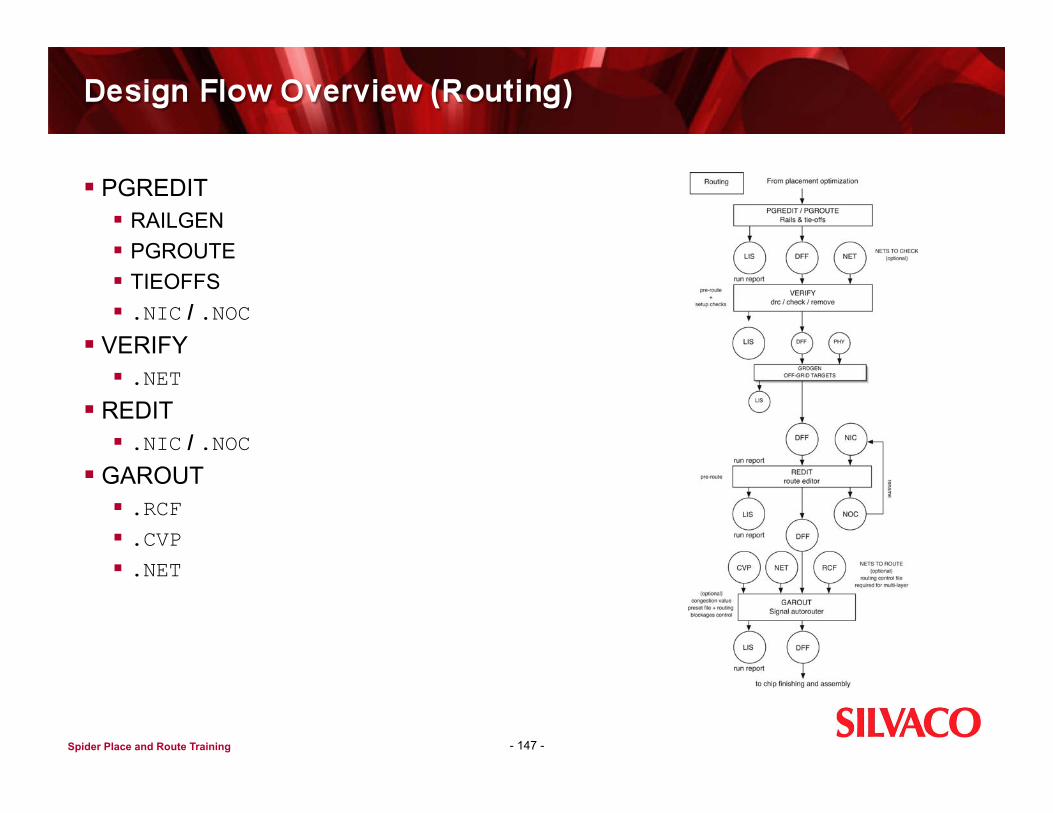
Spider Place and Route Training - 147 -
PGREDIT RAILGEN PGROUTE TIEOFFS .NIC / .NOC
VERIFY .NET
REDIT .NIC / .NOC
GAROUT .RCF .CVP .NET

Chip Finishing & Assembly Verification and RC Extraction
REDIT / RROUTE / RDUMP / RLOAD / MASKOUT / Expert / Guardian / HIPEX-RC / CLARITY-RLC
- 148 -

Spider Place and Route Training - 149 -
REDIT RROUTE
RDUMP RLOAD PDKs / PCELLs Expert
.TCN .GDS
Guardian DRC / LVS .LISA .NET
HIPEX-RC .SPICE .SPEF .DSPF
CLARITY-RLC .PORTS
RC & Timing Extraction
GADELAY / CAPCALC / SLTOSDF / WRITE_SYNOPSYS_PARASITICS / ACCUCORE STA
- 150 -

Spider Place and Route Training - 151 -
GADELAY .BACDLY .CLKDLY .PINDLY .PTHDLY .SUMDLY .SPICE
CAPCLC .REF .XTK .OVP .CAP
SLTOSDF (future update) .SDF
WRITE_SYNOPSYS_PARASITICS (future update) .DCS
ACCUCORE STA Verilog .v Liberty .lib SPICE / DSPF .spice .dspf

Spider GUI and Help System
GUI and Help Basics
- 152 -
Spider Place and Route Training
Press: Press a mouse button without releasing it often used to select an object
Release: Release a mouse button after pressing it often used to perform the action initiated by “dragging”
Click: Press and release a mouse button without moving the pointer. selects an object or performs an action The activation actually occurs on the release of the mouse button.
Double-click: Press and release a mouse button twice without moving the pointer combines selection and action in some dialog boxes
Drag: Press a mouse button without releasing it and then move the pointer position The drag action ends with a release action selects a range of objects or moves through a cascading menu
Select: Click on an item to select it
- 153 -
Spider Place and Route Training
ALL Spider Setup Parameter GUIs (except LOAD_DESIGN) can be accessed by typing:
> spider <module_name> <design> -setup ALL Spider Help can be accessed by typing: > spider <module_name> <design> -help ALL Spider Parameter status can be accessed by typing: > spider <module_name> <design> -info Modules having Run-time GUIs in addition to their Setup GUIs are:
GPLACE, PGREDIT, and REDIT
- 154 -

Spider Place and Route Training
Menu Bar – Drag left mouse to access menus from here. Status Bar – Details of Current Command State and XY position Display Area – Main graphic results display Scale Area – Displays current window relative to design space. Message Output Area – Non-Command messages Command Input Area – Text based entry and Command History XY-Ruler Areas – Left and Bottom of the Display Area Menus – Popup (press and hold right mouse button) and Cascading Dialog Boxes – parameters, values, and select objects Do not use the Full-Screen Cross-Hair at this time. Accessing the Spider GUI Command Line and History Dialog
DISPLAY -> Setup -> Command Input Area
- 155 -

Spider Place and Route Training - 156 -

Spider Place and Route Training
Control Buttons – OK (accept and close), Apply (accept and open), Filter (Open Dialog to control selection options), and Cancel (reset changes and close)
Scroll Bar – Slider is proportional to the displayed list size vs. total. Check Buttons – Filled is ON, unfilled is OFF (non-exclusive group) Radio Buttons – Filled is ON, unfilled is OFF (exclusive group) List Box – Displays a list of selectable data or selected data.
Filter based lists are NOT directly selectable (use By Net/Comp Name) Text Entry Box – Editable alpha-numeric data Number Entry Box – Editable number values Option Menu – Cascading sub-menu Command Button – Left-click to execute the specific command. Text Labels – Non-editable status information
- 157 -

Spider Place and Route Training - 158 -
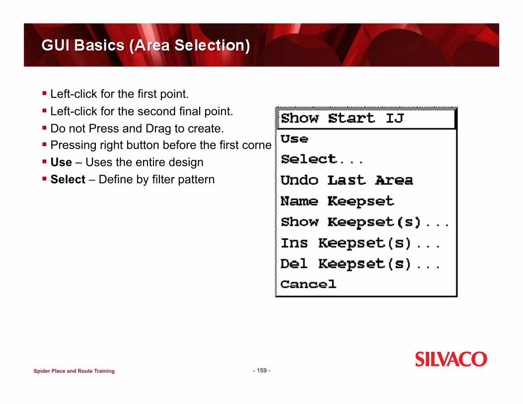
Spider Place and Route Training
Left-click for the first point. Left-click for the second final point. Do not Press and Drag to create. Pressing right button before the first corner selection displays ->. Use – Uses the entire design Select – Define by filter pattern
- 159 -

Spider Place and Route Training
When selecting Nets/Components, remember that direct list selection is impossible
Use the Filter to make selections and either add or delete them from the displayed list
Resetting the select list only resets Nets To Select display list
The main difference between Nets and Component selection are the Filtering options
- 160 -

Spider Place and Route Training
A: FILTER => A(keep); ADD; OK NOT(A): FILTER => A(remove); ADD; OK or ADD; FILTER => A(keep); DEL; OK A and B: FILTER => A(keep); FILTER => B(keep); ADD; OK A or B: FILTER => A(keep); ADD; RESET; FILTER => B(keep); ADD; OK A and NOT(B): FILTER => A(keep); FILTER => B(remove); ADD; OK or FILTER => A(keep); ADD; FILTER => B(keep); DEL; OK A or NOT(B): FILTER => A(keep); ADD; RESET; FILTER => B(remove); ADD; OK
- 161 -

Spider Place and Route Training
Keep – The matching filtered objects from the current “to select” list.
Remove – The matching filtered object from the current “to select” list.
Delete Item – Deletes highlighted objects from the current “selected” list.
Wildcards “*” Any number of characters (including
none) “-” Any one characters
- 162 -

LOAD_DESIGN
Netlist Import Management and Library Data Prep
- 163 -

Spider Place and Route Training
LOAD_DESIGN reads the input library and design files creating the *dl files necessary to initialize and compile the design
The DDL file is created separately by the LIB2DDL process and is required if you need to run CLKTREE
Using full path names is recommended if files are not in the current SPIDER working directory
- 164 -

Spider Place and Route Training
> spider load_design <design> -input <load_design>.load
- 165 -

Spider Place and Route Training
All values are in DF (microns*1000 by default). All parameters must end with “;”. Syntax must be exactly as shown with delimiter spacing as defined between ‘ ’, which define literal strings. “[ ]” define optional zero or more times. “#” is a comment
‘top_name = “’<top_level_module_name>‘” ;’
[‘verilog = “’<verilog_file>[‘ ’<verilog_file>]‘” ;’] [‘lef = “’<lef_file>[‘ ’<lef_file>]‘” ;’] [‘def = “’<def_file>‘” ;’] [‘tech = “’<technology_file>‘” ;’] [‘gridX = ’{‘off_by_halfgrid’ | ‘halfgrid’ | ‘fullgrid’}‘ ;’] [‘gridY = ’{‘off_by_halfgrid’ | ‘halfgrid’ | ‘fullgrid’}‘ ;’]
‘xsize = ’<int_number>‘ ;’ ‘ysize = ’<int_number>‘ ;’ [‘xoffset = ’<int_number>‘ ;’] (default 0) [‘yoffset = ’<int_number>‘ ;’] (default 0) ‘core_to_left = ’<int_number>‘ ;’ ‘core_to_bottom = ’<int_number>‘ ;’ ‘core_to_right = ’<int_number>‘ ;’
‘core_to_top = ’<int_number>‘ ;’ [‘unit = ’<units for micron>‘ ;’] (default 1000) [‘filler = “’<fill_cell_list>‘” ;’
- 166 -

Spider Place and Route Training
top_name : Specifies the name of the top level module for the design verilog : Specifies the file(s) containing the gate level netlist in verilog format.
Generates <design_name>.spider.def, if verilog = is specified lef : Specifies the file(s) containing the physical Blockage/Pin/Via (BPV)
information for the cells in the library in LEF format When LEF data is provided, all library cells in the LEF are processed regardless of use in
the netlist Also, a pin access check and report is performed on all the cells in the LEF Pins will be “on grid” the maximum extent possible
tech : Specifies the file containing the LEF technology header information (non-cell section). May be the same file as the lef = file
- 167 -

Spider Place and Route Training
gridX (gridY) : Specifies the vertical (horizontal) routing grid. fullgrid : Specifies to start the routing grid at the placement grid and step in unit tile
(i.e.,"fullgrid“) increments at the pitch specified in the LEF technology header section. halfgrid : Specifies to start the routing grid at the placement grid and step in half the
unit tile (i.e.,"halfgrid“) increments at half the pitch specified in the LEF technology header section Using this option permits wire spreading and additional spacing or wire width without
losing a full routing track wide Permits support for cells designed on a half grid pitch without needing to resort to "offgrid"
routing methods using GRDGEN off_by_halfgrid (default): Specifies to start the routing grid with half a unit tile
(i.e.,"halfgrid“) to offset from the placement grid and step in unit tile (i.e.,"fullgrid“) increments at the pitch specified in the LEF technology header section
xsize, ysize : Specifies the design space limits for the chip or block (DIEAREA) While not required to be units of the routing pitch (or cell pitch), blocks should be unit to
allow easy integration in hierarchical designs xoffset, yoffset : Specifies the offsetting of the GDSII origin of the design
space to ease final chip assembly Origin offset for xsize and ysize DIEAREA It has no other purpose or impact to the design process
- 168 -

Spider Place and Route Training
core_to_left, core_to_bottom, core_to_right, core_to_top : These four parameters specify the start and stop limits of the placement grid relative to the defined design limits of the chip or block They should be used together as a group The placement grid starts bottom left justified and extends in unit tile values of the
placement grid until reaching the placement limits It is recommended that the values be units of the routing pitch
unit : Specifies the ratio of design units to physical units in the database. Normally, the default value should be used An alternate value could be 10000 or 100 as suitable for a given technology
filler : Specifies an optional list of GDSII cell library filler cells to occupy unplaced row locations in a design. Filler cells should be listed in order from smallest to largest. MASKOUT will insert these filler cells from largest to smallest in available ROW placement locations, minimizing the number of filler cells inserted
- 169 -

Spider Place and Route Training
verilog : When specifying verilog =, def = cannot be used. When defining multiple files the list must be enclosed in “”.
lef : When defining multiple files, the list must be enclosed in “”. You can accommodate pins “off grid” by running GRDGEN before the routing
phase. Only a limited number of total grids in X and in Y are permitted 20000 in each direction for the entire chip/block Pin access checks are not performed on GDSII converted to PDL directly through
the GDSGDL and GDLPDL conversion utilities LEF data should be processed before any GDSII to provide .wid information to the
GDSII conversion process, so PDLs can be easily merged Any changes to the physical data may require you to reprocess all physical data to
assure proper wire width index definition control, unless you don’t need any new wire widths.
def : When specifying def =, verilog = cannot be used While reading DEF is supported, not all features of the DEF syntax are
Currently, only COMPONENTS, DIEAREA, NETS, PINS, SPECIALNETS and pre-routing are supported. ROWS, REGIONS, and other floorplanning related features including pre-placement from physical synthesis are not
tech : This is required if lef = is specified
- 170 -

Spider Place and Route Training
gridX, gridY halfgrid : Selecting this option reduces the maximum chip size by half since a max of
20000 routing grids is permitted in the X direction core_to_left, core_to_bottom, core_to_right, core_to_top : The
placement grid is rectangular only Unused sections should be defined with placement obstructions (or another method) in
GPLACE and can be read or written to an .obs file Do not allow placement grids to start and end at the chip or block extent limits. ROWS always:
run in the horizontal direction "doubleback" 100% placement density the first row is "normal" (non-rotated) orientation
If you want to run ROWS vertically, then swap the desired X and Y dimensions and rotate the final block or the padframe reference point accordingly
No mixed orientations of ROWS is allowed However, you make separate block sections to allow this effect during the final chip
assembly by using hierarchical methods
- 171 -

GDSGDF and GDFPDL
GDSII Physical Modeling Blockage / Pin / Via (BPV)
- 172 -

Spider Place and Route Training - 173 -
Run GDSGDF first one time to pre-filter layers unneeded for P and R view generation
Run the GDFPDL process without any width information defined in the WID file. At the bottom of the created PDL (in a comment) will be the required .wid file information to eliminate automatically created OBSTRUCTION data
OBSTRUCTION data is not associated with any pins (even if required to be)
Add the auto created .wid information to the .wid file (remembering to exclude the comment markers) and then re-run GDFPDL only with the new .wid file
If any new .obs data is present at the end of the .pdl file, repeat the process including the new .wid information

Spider Place and Route Training - 174 -
Run GDSGDF first one time to pre-filter layers unneeded for P and R view generation
Run GDFPDL the same as before for without LEF, except start by including the required .wid data by editing the data in the generated TDL into .wid format and then run through the SAME GDFPDL processing steps
Doing this will ensure that the PDL created by the LOAD_DESIGN process from the LEF data remains correct regarding width index references
Do not try to process the GDSII first before the LEF! Otherwise, attempts to merge the two resulting PDLs will be problematic due to different width reference data and will need significant editing to correct!

Spider Place and Route Training
> spider gdsgdf <design> [<parameters>]
- 175 -

Spider Place and Route Training - 176 -
-gds_file <file_name>.gds -listing <file_name>.lis -layer_file <file_name>.lyr -gdf_file <file_name>.gdf
-filter_layers {‘t’|‘f’} -overwrite {‘t’|‘f’}

Spider Place and Route Training - 177 -
For GDSGDF to pre-filter layer data, a LYR file must define the data in the GDSII relative to Spider required layers
This is a simple file like shown below: ! This is a comment in a LYR file
M1 DATA <layer_#> <data_type_#> so is this
V1 DATA <layer_#> <data_type_#>
M2 DATA <layer_#> <data_type_#> … TRGM1 TEXT <layer_#> <data_type_#>
… ! Does NOT control placement
OUTLINE DATA <layer_#> <data_type_#>
Other special layers exist for special modeling options, see the Spider Reference Manual for details

Spider Place and Route Training
GDSGDF converts GDSII and pre-filters unnecessary data to simplify the BPV process in creating P and R cell views
GDFPDL performs the actual BPV process extracting connectivity from the geometry and formatting the resulting physical data into Physical Design Library (PDL) syntax
Cell names must be unique within the first 20 characters and names less than 20 characters will be truncated and converted to uppercase
Do not flatten data! This will complicate BPV processing Any change in any physical cell requires that you reprocess all cells if any TDL
widths or WID file changes are required to do so Non-orthogonal geometry (X and Y only) will be converted to a “bounding box”,
possibly creating pin access issues. Pre-edit the GDSII data to minimize this problem by breaking down geometry into rectangles whereever possible. Expert can easily perform this task to the entire GDSII file in one simple pass
If the LEF contains required polygon objects, then GDSII -> PDL conversion is the only option here
- 178 -

Spider Place and Route Training
> spider gdfpdl <design> [<parameters>]
- 179 -

Spider Place and Route Training - 180 -
-listing <file_name>.lis -gdf_file <file_name>.gdf -namelist <file_name>.nam -widthlist <file_name>.wid -pdl <file_name>.pdl
-autointern {‘t’|‘f’} -expandall {‘t’|‘f’} -expandtarg {‘f’|‘t’} -genconpads {‘f’|‘t’} -nca_naming {‘f’|‘t’}

Spider Place and Route Training - 181 -
Case independent and limited to 80 characters/lines (other than comments) You can process illegal SDL characters in cell names by adding BADCHARWARN
as the first line. But this results in editing PDL before running PCOMP This is a simple file like shown below: ! This is a comment line ! See the Spider Reference Manual for additional details ! (especially for PADCELLs) PADCELL <cell_name> optional … (list all support “rectangle” cells (not I/O pad cells) PDLCELL <cell_name> … (list all primitive gates “cells” to process) VIA1CELL <via1_cell_name> optional (one time only) VIA2CELL <via2_cell_name> optional (one time only) … (list all via cells, one per via layer) GLOBALNAME VDD VDD use VCC or some other name as required GLOBALNAME VSS VSS use GND or some other name as required … (list all global nets common to all cells)

Spider Place and Route Training - 182 -
Limited to 500 characters/lines and 500 widths per layer Width index 1 is reserved so .wid values start at the 2nd index value UNITS are in DF (i.e., 1000 per micron) This is a simple file like shown below: ! This is a comment line
! See the Spider Reference Manual for additional details
METAL1 <width_list> (space separated)
… (specify multiple times as needed in order but not required to be in size sequence) METAL2 <width_list>
… (list all routing layers not vias) ! set other than 1 (max min_width/2)
! if targets exist not on geometry
TARGETSIZE 1
Spider Place and Route Training - 183 -
Carefully review all warnings. Most routing problems trace back to modeling. GDFPDL is not intended to model complex soft macros in full detail. Also,
processing full detail SRAMs is possible but may require long run-times. Pre-editing SRAMs to replace the bitcell array with a single blockage is the best way to do this, but this is optional. You can use the Spider OBSM<#> LYR object to “clip” unneeded detail data from a general obstruction region
OBSM<#> objects must be rectangles (or orthogonal wires) When using PDL from GDFPDL, make sure that in the TDL file “OBSTRUCTION_BOUNDARY METAL_EDGE” is defined and not “LITERAL” Only Routing layers and cuts (vias/contacts) are modeled and connectivity cannot
be derived from other layers Model Poly (if required) as the first routing layer and reference it to M1 (really
LAYER1). M1 then references to M2 (really LAYER2) and so on Be very carefully if you model with Poly to avoid diffusion related errors. Poly
should only be used if necessary (i.e., M1 (or M2) only process) You should not include Poly for RC timing purposes only
Spider Place and Route Training
Spider is a GRIDDED router and works based on “targets” and “obstructions”, not actual geometry
Routing is complete if a target is reached. The max grids in X (or Y) are each 20000 You should use a regular grid network Targets (in different layers) are prohibited to co-locate at the same exact X and Y
for different pins. Targets, however, are permitted for the same pin if you define a “multi-layer” target instead of two (or more) single-layer targets (e.g., TRGM12 vs. TRGM1 and TRGM2)
Define multi-layer targets using separate layer assignments from different GDSII layers without auto-infer
Define optional geometry separately from different GDSII layers. Both multi-layer targets and optional geometry are advanced topics and are not
covered here. Consult an AE if they are required. The first target defines:
placement wire length calculations between pins various Spider features
- 184 -

Common *DL File Syntax
CDL / TDL / PDL / DDL
- 185 -

Spider Place and Route Training
“PAD” as it relates to *DL files refers to a rectangular geometry object It is not an I/O pad “SEG” or “SEGMENT” that refers to a wire or “path” object As it relates to <number_range>
<count> is the number of items, including the one at <start_number>. A missing <step> is equivalent to ‘!1’.
{A:Z | a:z | 0:9 | ‘_’ | ‘#’ | ‘$’ | ‘<’ | ‘>’} <'any'_name> ::= 1 to 20 characters from the set: <digit> ::= {0:9} <number> ::= [‘-’]<digit>[<digit>] <delay> ::= {0:15} <orientation> ::= {0:7} <np> ::= <number>‘.’<number> <number_range> ::= <number> | {<start_number>‘-’<end_number>[‘!’[‘!’]<step>]} | <start_number>‘*’<count>[‘!’[‘!’]<step>] <number_list> ::= <number_range>[‘,’<number_range>] <np-range_pair> ::= <number_range>‘.’<number_range> <np-list> ::= <np-range_pair>[‘,’<np-range_pair>] <np_ori_list> ::= <np-range_pair>‘+’<orientation>[‘,’<np-range_pair>‘+’ <orientation>]
<string> ::= 0 to 200 chars from the set of all printable characters
- 186 -

Spider Place and Route Training
<attribute> ::= <attribute_name>‘=’{‘<string>’|“<string>”}] <attribute_list> ::= ‘(’<attribute>[‘,’<attribute>]‘)’ <layer> ::= <layer_name> <layer_range> ::= ‘[’<layer>‘–’<layer>‘]’ <obstlayer> ::= {<layer> |<layer_range> |‘PLACEMENT’ |‘ALL’ |‘VIA’[‘[’{<layer>|<layer_range>|‘ALL’}']']} <obstruction_definition> ::= ‘OBST:’{<obstlayer>|{‘DELAY’‘+’<delay>}}‘*’<np> ‘@’<np-list>‘;’
<target_statement> ::= {‘TARGET:’|‘OPTTARGET:’}<target_layer>‘@’<np-list>‘;’ <target_layer> ::= <layer> |<layer_range> |‘ALL’ |{‘CONTACT’‘*’<pad_name>‘+’ <orientation>} <segment_definition> ::= {‘SEG:’|‘OPTSEG:’|‘UNCSEG:’}<layer>‘*’ <line_width_index>‘@’<start_np>‘-’<end_np>‘;’
<via_definition> ::= {‘VIA:’|‘OPTVIA:’|‘UNCVIA:’} [‘[’<layer>‘]’[‘+’<orientation>]‘@’]<np-list>‘;’ <pad_definition> ::= {‘PAD:’|‘OPTPAD:’|‘UNCPAD:’}<layer>‘*’<pad_name>‘+’ <orientation>‘@’<np-list>‘;’
- 187 -

Spider Place and Route Training
<physical_routing> ::= [<segment_definition> | <via_definition> | <pad_definition>]
<cell_net> ::= ‘CELLNET’ [<attribute_list>]; (* Attributes are ignored *) <physical_routing> ‘ENDNET;’
<global_net> ::= ‘GLOBALNET:’ <chip_physical_type_pin_name> ‘;’ [<target_statement>] <physical_routing> ‘ENDNET;’
- 188 -

CDL Syntax
Chip Description Library
- 189 -

Spider Place and Route Training
The Chip Description Library (CDL) describes routing layers, preferred routing direction on layer 1, usable chip area, and fixed-location cells for placement purposes
Additionally, the CDL refers to the physical type (base array or master slice) containing chip routing and chip obstructions and specifies the technology used on the chip
LOAD_DESIGN generates the CDL in only a limited design style for chip initialization (uniform single “doubleback” horizontal row area) Spider supports many other design styles, however, you must manually edit/
create them in the CDL to use them DATAPATH style Irregular/non-uniform ROW locations and orientations Gate-array style Special macro floorplanning options Other design styles
- 190 -
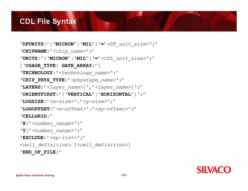
Spider Place and Route Training
‘DFUNITS:’{‘MICRON’|‘MIL’}‘=’<DF_unit_size>‘;’ ‘CHIPNAME:’<chip_name>‘;’ ‘UNITS:’{‘MICRON’|‘MIL’}‘=’<CDL_unit_size>‘;’ [‘USAGE_TYPE: GATE_ARRAY;’] ‘TECHNOLOGY:’<technology_name>‘;’ ‘CHIP_PHYS_TYPE:’<phystype_name>‘;’ ‘LAYERS:’<layer_name>[‘,’<layer_name>]‘;’ ‘ORIENTFIRST:’{‘VERTICAL’|‘HORIZONTAL’}‘;’ ‘LOGSIZE:’<x-size>‘.’<y-size>‘;’
‘LOGOFFSET:’<x-offset>‘.’<xy-offset>‘;’ ‘CELLGRID:’ ‘X:’<number_range>‘;’ ‘Y:’<number_range>‘;’ ‘EXCLUDE:’<np-list>‘;’ <cell_definition> [<cell_definition>]
‘END_OF_FILE;’
- 191 -

Spider Place and Route Training
CELLNAME:<cell_name> ‘;’ SIZE:<x-size>‘.’<y-size>‘;’ [OFFSET:<x>‘.’<y>‘;’] [POS:<np-range_pair>‘+’<orientation>][‘,’<np-range_pair>‘+’ <orientation>]‘;’]
[MATRIXSIZE:<I> ‘.’ <j>; [CUTOUT:<np-list>] [EXCLUDE:<np-list>] MATRIXPOS:<offset>‘+’<ori>‘@’<np-list>‘;’ [MATRIXPOS:<offset>‘+’<ori>‘@’<np-list>‘;’]] [<global_net>]
[<cell_net>]
[<obstruction_definition>]
‘ENDCELL;’
- 192 -

TDL Syntax
Technology Description Library
- 193 -

Spider Place and Route Training
The Technology Description Library (TDL) describes the technology aspects of the design
The TDL allows you to describe the grid size, line widths, line-to-line spacing, line-to-pad spacing, pad-to-pad spacing, and pad sizes used on the chip
Additionally, the TDL allows you to specify via pad sizes for each routing layer
Since vias are symbolic, any via design rule can be supported including multiple vias per connection for redundancy
- 194 -

Spider Place and Route Training
Manual edits to the LOAD_DESIGN automatically create TDL from the LEF may be required to address “special” Design Rule issues
Only either a single via per layer or a single via per layer per width pair combination is supported If the LEF contains multiple via definitions for the same via, you will need to edit the TDL to use
only one (typically the default) Matrix vias (for wide metal) are supported by reference to multiple individual vias only. Vias are symbolic in Spider. Only cell references (SREFs) are provided in the GDSII and
must be replaced like all other cells with their final GDSII versions Make sure the via definitions in the TDL and the actual vias used for the GDSII match in
footprint or DRC issues can occur If via adjacency design rules limit due to density and not by metal spacing:
Then to ensure compliance when defining the routing grid structure and via adjacency rules in the TDL, define routing grids in a manner that vias can be dropped as follows: without rotation without offset and on grid
Wire routing always terminates with a W/2 extension on grid. End-of-line and min-area rules are supported through via definitions only or existing cell pin
geometry
- 195 -

Spider Place and Route Training
‘TECHNOLOGYLIB:’<tech_library_name>‘;’ (* For reference only *) ‘UNITS:’{‘MICRON’|‘MIL’}‘=’<number>‘;’ <technology_description> [<technology_description>]
<spec_set_definition> [<spec_set_definition>]
<pad_definition> [<pad_definition>]
‘END_OF_FILE;’
- 196 -

Spider Place and Route Training
TECHNAME: <technology_name>‘;’ [{<regular_grid>|<variable_grid>}] (* A global grid is optional *) [TOLERANCE:<number>‘;’ ‘CONTACTMASK:’{‘FIXED’|‘PROGRAMMABLE’}‘;’ [‘VIAS_ON_CONTACTS:’ {‘YES’|‘NO’}‘;’] (* A global rule is optional *) [‘NO_ADJ_SAME_NET_VIAS:’{‘YES’|‘NO’}‘;’] ‘OBSTRUCTION_BOUNDARY:’{‘LITERAL’|‘METAL_EDGE’}‘;’ [‘ONE_PIN_NET_HANDLING:’ {‘GEN_OPT_FEATURES’ | ‘GEN_UNC_FEATURES’|‘NO_OPT_UNC_FEATURES’}‘;’] <layer_specs> ‘ENDTECH;’
<regular_grid> ::= ‘GRIDSIZE:’<number>[‘.’<number>]‘;’ <variable_grid> ::= ‘VARIABLEGRID:’ ‘X_GRID:’<number_list>‘;’ ‘Y_GRID:’<number_list>‘;’ <layer_specs> ::= ‘ALL’ ‘=’ <spec_set_name> | <layer>‘=’<spec_set_name>[‘,’<layer>‘=’<spec_set_name>]‘;’
- 197 -

Spider Place and Route Training
‘SPECSETNAME:’<spec_set_name>‘;’ [‘GRID:’<number_list>‘;’] (* Per-layer preferred grid *) ‘LINE_PAD:’<number>‘;’ ‘PAD_PAD:’<number>‘;’ ‘VIAPAD:’<pad_name>‘+’<orientation>[‘,’<pad_name>‘+’<orientation>]‘;’ [‘STACK_OK:’{‘YES’|‘NO’}‘;’] (* Defaults to VIAS_ON_CONTACTS *) ‘LINE_SPECS:’<line_width> ‘&’ <line-line_spacing> [‘,’<line_width>‘&’<line-line_spacing> ]; ‘ENDSPECSET;’
Either the old global regular/variable grid or the GRID statement per layer is used but not both If a global grid is specified, all odd-numbered layers will have the same preferred grid in one
direction and all even-numbered layers will have the same preferred grid in the other direction Per-layer grids are prohibited for one-layer designs Assume N layers [1 : N] Layer 1 spec set needs only one pad (bottom pad of 1:2 via), and Layer M (M = [2 : N-1]) spec set needs two pads:
1st pad: top pad of M-1:M via 2nd pad: bottom pad of M:M+1 via
Layer N spec set needs only one pad (top pad of N-1:N via)
- 198 -

Spider Place and Route Training
‘PADNAME:’<pad_name>‘;’ ‘PADSIZE:’<width>‘.’<height>[‘.’<x_offset>]‘;’ [‘CUTPAD:’<pad_name>[‘+’<orientation>]‘;’] [‘VIASTACK:’<layer>‘*’<np>‘@’<np>[‘,’<layer>‘*’<np>‘@’<np>]‘;’] ‘ENDPAD;’
VIASTACK is used to define the via stacking rules using explicit via obstructions in remote higher-numbered layers (e.g., 2:3 vias over layer 1 pads) and should be associated with CONTACT pads or the top pad of any via
The stacking of vias/contacts sharing a common layer is controlled by that layer's STACK_OK statement (or VIAS_ON_CONTACTS)
Interaction with contacts of vias starting in lower-numbered layers is defined by the VIASTACK statements for those lower-layer objects
The explicit reference to the obstructed layer will probably mean that in designs with less than 2 layers (the only ones where VIASTACK is valid), same size pads but in different layers should be different Spider pads
- 199 -

PDL Syntax
Physical Description Library
- 200 -

Spider Place and Route Training
The Physical Description Library (PDL) describes the physical characteristics of the logical types used in the design
It defines the logical-physical correspondence and the layout of the physical types
You should have cell library pin target locations be accessible on grid with a regular matrix structure
- 201 -

Spider Place and Route Training
While support for OFF GRID pins exists in Spider, it is limited to 20000 grids in each of X and Y for the entire design including any regular matrix grid locations
Libraries with irregular grid pin access will likely require modification for full support and maximum route completion and design density
LOAD_DESIGN performs a pin access and grid check on the LEF it uses to generate PDL. However, GDSGDF & GDFPDL do not and are driven by text labeling or a dedicated GRID layer during import and conversion
Spider does not check cell physical geometry vs. cell physical geometry.Therefore, cells must be DRC clean when placed in all possible cell locations, combinations, and orientations
Connections by abutment (or overlap) are not allowed Placement obstructions are only permitted in the chip_physical_type
- 202 -

Spider Place and Route Training
‘PHYSICALLIB:’<physical_library_name>‘;’ (* For reference only *) ‘UNITS:’{‘MICRON’|‘MIL’}‘=’<number>‘;’ <logical-physical_matching>
‘END;’ <physical_type_definition> [<physical_type_definition>]
‘END_OF_FILE;’
<logical-physical_matching> ::= <logical_type_name>‘=’ <physical_type_name>[‘,’<physical_type_name>]‘;’
<physical_type_definition> ::= <primitive_physical_type>
| <chip_physical_type>
- 203 -

Spider Place and Route Training
‘PHYSICALNAME:’ <physical_type_name>‘;’ ‘CELL:’<celltype_name>‘;’ [‘OUTLINE:’<np-list>‘;’] ‘NPINS:’<number>‘;’ [‘NAME_OFFSET:’<np>‘;’] [‘EXTNAME_OFFSET:’<np>‘;’] (* Syntax correction *) [<target_net>]
[<global_net>] (* Added for PG taper *) [<internal_net>]
[<obstruction_definition>]
‘ENDPHYSICAL;’
- 204 -

Spider Place and Route Training
‘PHYSICALNAME:’<chip_physical_type_name>‘;’ [‘OUTLINE:’<np-list>‘;’] ‘NPINS:’<number>‘;’ [<target_net>]
[<internal_net>]
[<obstruction_definition>]
‘ENDPHYSICAL;’
- 205 -

Spider Place and Route Training - 206 -
<target_net> ::= ‘TARGETNET:’ <pin_name> [<attribute_list>]‘;’ <target_statement> [<target_statement>]
[<physical_routing>]
‘ENDNET;’
<internal_net> ::= ‘INTERNALNET’ [<attribute_list>]; (* Attributes *) (* ignored w/ warning *) <physical_routing>
‘ENDNET;’

DDL Syntax
Delay Description Library
- 207 -

Spider Place and Route Training
The Delay Description Library (DDL) specifies the scale and resolution of time, capacitance, and resistance values, specifically: sheet resistance and per-unit area capacitance of all layers electrical properties of contacts and vias electrical properties and pin-to-pin delays of each macro in the library
This information is necessary to perform clock-tree synthesis using CLKTREE and delay analysis for each net and path using GADELAY or CAPCLC
Spider constructs an RC tree of all wiring segments and contacts for pin-to-pin delay calculation
A SPICE-like simulation is performed on the RC tree in the context of the driving function and the receiving inputs
During this time domain simulation, delays are measured when input signals reach the appropriate threshold level
LIB2DDL will generate the “macro model” section of this file
- 208 -

Spider Place and Route Training
If an <rc_specification> section is included in the DDL file, then each <macro model> section must also include RC statements
Calculating CONTACTCAP and VIACAP values can be tedious Make sure they will have a significant effect before performing the calculations
Consider all potential error sources when constructing a DDL RC header and margin accordingly
- 209 -

Spider Place and Route Training
‘TIMINGLIB:’<timing_library_name>‘;’ ‘TIME_BASE:’<number>‘;’ ‘TIME_RESOLUTION:’<number>‘;’ ‘CAP_BASE:’<number>‘;’ (* -12 is std *) ‘CAP_RESOLUTION:’<number>‘;’ (* -21 is std *) ‘CAPTOBULK:’<layer>‘=’<cnumber>[‘,’<layer>‘=’<cnumber>]‘;’ [‘SQRUNITCAP:’<layer_range>‘=’<cnumber> [‘,’<layer_range>‘=’<cnumber>]‘;’] [‘FRINGECAP:’<layer>‘=’<cnumber>[‘,’<layer>‘=’<cnumber>]‘;’]
‘CONTACTCAP:’<cnumber>‘;’ ‘VIACAP:’<layer>‘=’<cnumber>[‘,’<layer>‘=’<cnumber>]‘;’ [<rc_specification>]
<macro_model> [<macro_model>]
‘END_OF_FILE;’ NOTE: <layer_range> ::= [<layer>‘-’<layer>] Example: [METAL1 – METAL2]
- 210 -

Spider Place and Route Training
‘RCTIMING;’ ‘RES_BASE:’<number>‘;’ (* 0 is std *) ‘RES_RESOLUTION:’<number>‘;’ (* -3 is std *) ‘THRESHOLD_PERCENT:’‘LH’‘=’<number>‘,’‘HL’‘=’<number>‘;’ (* 50 is std *) ‘SHEET_RESISTANCE:’<layer>‘=’<rnumber>[‘,’<layer>‘=’<rnumber>]‘;’ ‘CONTACTRES:’<rnumber>‘;’ ‘VIARES:’<layer>‘=’<rnumber>[‘,’<layer>‘=’<rnumber>]‘;’ ‘END;’
- 211 -

Spider Place and Route Training
‘PHYSICALNAME:’<physical_type_name>‘;’ [<input_model> | <output_model> | <bidirect_model>] [<intrinsic_delay_spec> | <setup_delay_spec>] ‘ENDPHYSICAL;’
<input_model> ::= ‘INPUT:’{<input_pin_name>|‘*’}‘;’ ‘CIN:’<cnumber>‘;’ [‘RC:’‘RIN’‘=’<rnumber>‘;’] ‘END;’
<output_model> ::= ‘OUTPUT:’{<output_pin_name>|‘*’}‘;’ ‘INC_CAP:’<cnumber>‘;’ ‘INC_TLH:’<tnumber>‘;’ ‘INC_THL:’<tnumber>‘;’ [‘CIN:’<cnumber>‘;’] [‘RC:’‘COUT’‘=’<cnumber>‘,’‘RLH’‘=’<rnumber>‘,’‘RHL’‘=’<rnumber>‘;’] ‘END;’
- 212 -

Spider Place and Route Training
‘BIDIRECT:’{<bidirectional_pin_name>|‘*’} ‘;’ ‘INC_CAP:’<cnumber>‘;’ ‘INC_TLH:’<tnumber>‘;’ ‘INC_THL:’<tnumber>‘;’ ‘CIN:’<number>‘;’ [‘RC:’‘RIN’‘=’<rnumber>‘,’‘COUT’‘=’<cnumber>‘,’ ‘RLH’‘=’<rnumber>‘,’‘RHL’‘=’<rnumber>‘;’] ‘END;’
- 213 -

Spider Place and Route Training
‘INT_DLY:’{<input_pin_name>|<bidirect_pin_name>|‘*’}‘–’ {<output_pin_name>|<bidirect_pin_name>|‘*’}‘=’{‘I’|‘N’|‘X’} ‘,’‘TLH’‘=’<tnumber>‘,’‘THL’‘=’<tnumber>‘;’
NAND3 Example: INT_DLY: A - Z = I,
TLH = 0.21,
THL = 0.26;
INT_DLY: B - Z = I,
TLH = 0.27,
THL = 0.22;
INT_DLY: C - Z = I,
TLH = 0.33,
THL = 0.19;
- 214 -
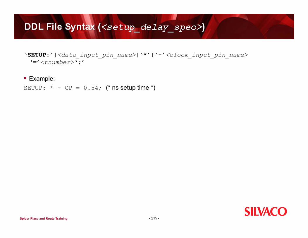
Spider Place and Route Training
‘SETUP:’{<data_input_pin_name>|‘*’}‘-’<clock_input_pin_name> ‘=’<tnumber>‘;’
Example: SETUP: * - CP = 0.54; (* ns setup time *)
- 215 -

SDL Syntax
Structure Description Library Spider Netlist Format
- 216 -

Spider Place and Route Training
Comments begin with “(*” and end with “*)” are block style and may be embedded except within a name.
All statements (not lines) end with “;”. Lines must be less than 80 characters. Valid characters: 0…9 A…Z _ # @ $ / “< >” or “[ ]” are Bus Elements. “<:>” or “[:]” and “<,>” or “[,]” are Buses (Ranges and Lists). Arrays are prohibited. Case independent Names are limited to 20 characters for uniqueness (or translated to be
so). No embedded spaces Global Nets are defined by “@” prefix.
- 217 -

Spider Place and Route Training - 218 -
ALIAS BIDIRECT CEND COMPSEGMENT END ENDC ENDCOMPS ENDIMPLS ENDMARCO ENDNETS END_OF_FILE EQUIVALENCE EXT EXTCONNECTOR
FROM IMPLSEGMENT INPUTS LEVEL MACRO NETSEGMENT NULL OUTPUTS PURPOSE TO TYPES USER USERNAME

Spider Place and Route Training
‘USER:’ <user>‘;’ <circuit> [<circuit>]… ‘END_OF_FILE;’
- 219 -
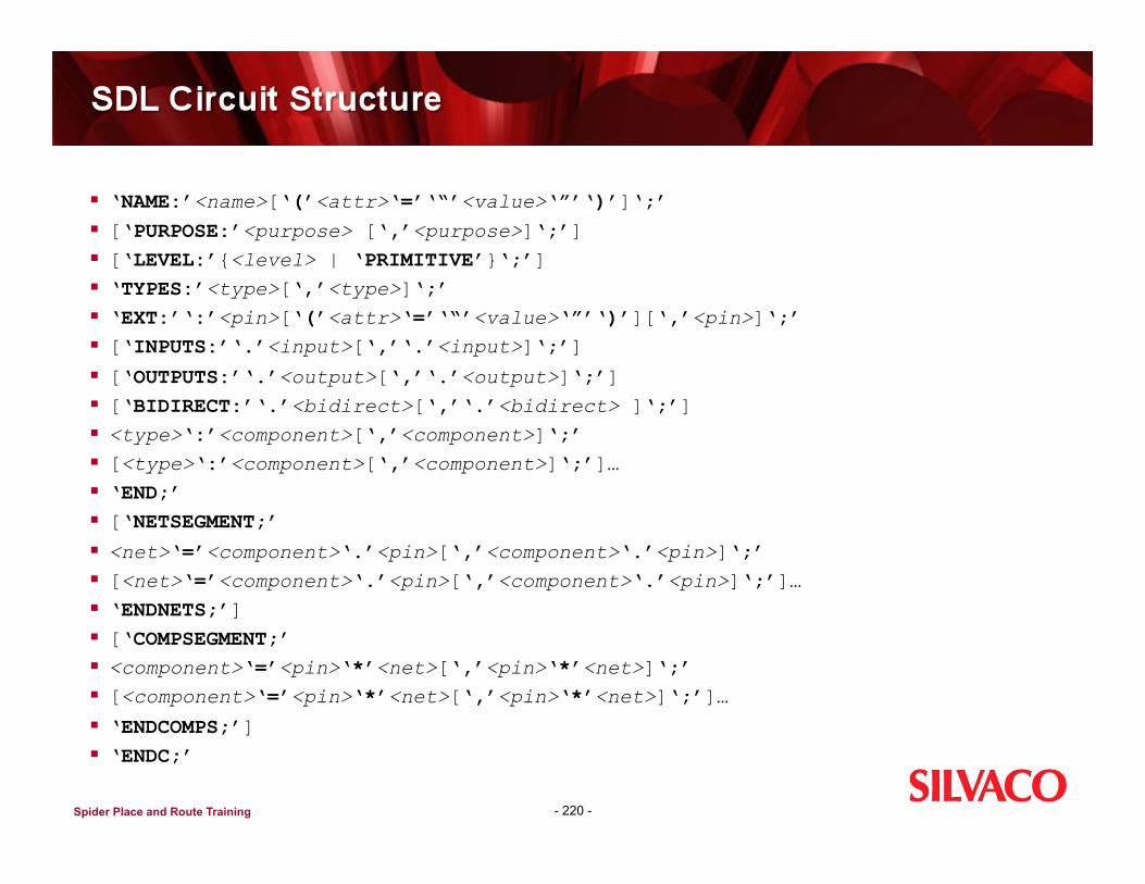
Spider Place and Route Training
‘NAME:’<name>[‘(’<attr>‘=’‘“’<value>‘”’‘)’]‘;’ [‘PURPOSE:’<purpose> [‘,’<purpose>]‘;’] [‘LEVEL:’{<level> | ‘PRIMITIVE’}‘;’] ‘TYPES:’<type>[‘,’<type>]‘;’ ‘EXT:’‘:’<pin>[‘(’<attr>‘=’‘“’<value>‘”’‘)’][‘,’<pin>]‘;’ [‘INPUTS:’‘.’<input>[‘,’‘.’<input>]‘;’] [‘OUTPUTS:’‘.’<output>[‘,’‘.’<output>]‘;’] [‘BIDIRECT:’‘.’<bidirect>[‘,’‘.’<bidirect> ]‘;’] <type>‘:’<component>[‘,’<component>]‘;’ [<type>‘:’<component>[‘,’<component>]‘;’]… ‘END;’ [‘NETSEGMENT;’ <net>‘=’<component>‘.’<pin>[‘,’<component>‘.’<pin>]‘;’ [<net>‘=’<component>‘.’<pin>[‘,’<component>‘.’<pin>]‘;’]… ‘ENDNETS;’] [‘COMPSEGMENT;’ <component>‘=’<pin>‘*’<net>[‘,’<pin>‘*’<net>]‘;’ [<component>‘=’<pin>‘*’<net>[‘,’<pin>‘*’<net>]‘;’]… ‘ENDCOMPS;’] ‘ENDC;’
- 220 -

Spider Place and Route Training
Component NAME Attributes (TYPE = “EMBEDDED”) (SL_SIZE = “10”)
EXT Pin Attributes (GARDS_SAVE = “ ”) (EQ_CLASS = “<logic_type_class>”) (GEN_EXT_NAME = “<pad_name>”)
For a “cell” to be defined as a block, it must: have a (TYPE = “EMBEDDED”) attribute
Only “embedded” blocks can use the Block Ring Router in PGREDIT. To support P and G routing including “tie-offs”, these nets must:
be declared as top-level EXT pins must have a GARDS_SAVE attribute be located at “legal” pin sites
- 221 -

Spider Place and Route Training
PCOMP ignores top-level EXT pins without a GARDS_SAVE attribute “1 pin” nets
To enable “pin-swapping” EXT pins must: have the EQ_CLASS attribute defined in the SDL component section
To add LVS text names to the layout generated by MASKOUT: I/O Bond Pads should use the GEN_EXT_NAME attribute
- 222 -

Spider Place and Route Training - 223 -

Spider Place and Route Training - 224 -
USER: "SDL DOCUMENTATION"; NAME: M82;
PURPOSE: SIMULATION;
LEVEL: GATE;
TYPES: XOR2, XNOR2, INVERTER, A05;
EXT: :B<1>, A<1>, B<0>, A<0>, CI, S<1>, CO, S<0>;
INPUTS: .B<1>, .A<1>, .B<0>, .A<0>, .CI;
OUTPUTS: .S<1>, .CO, .S<0>;
XOR2: X3, X2, X1;
XNOR2: XN1;
INVERTER: INV2, INV1;
A05: COMP2, COMP1;
END;
NETSEGMENT;
NB1= INV1.A, X3.2, .B<1>; NA1= X3.1, INV2.A, .A<1>;
NX3= X3.3, XN1.2;
NXN1= .S<1>, XN1.3;
NX2= .S<0>, X2.3;
CN= COMP1.Z, COMP2.A, XN1.1;
NB0= COMP1.C, .B<0>, X1.2;
NA0= COMP1.B, .A<0>, X1.1;
NX1= X1.3, X2.2;
NC0= COMP1.A, .CI, X2.1;
NI2= INV2.Z, COMP2.B;
NI1= INV1.Z, COMP2.C;
COMP2_Z= COMP2.Z, .CO;
ENDNETS;
ENDC;
END_OF_FILE;

SLNET
Netlist Pre-Processor / Compiler
- 225 -

Spider Place and Route Training
Expands a hierarchical SDL netlist flattening (and “bit-blasting”) the design (and buses) down to gate level library primitives and single pins (bus pins are not supported in layout)
Defines additional cells for synthesis/optimization operations Creates an NDB file for use by PCOMP Stores hierarchical cross-reference information for the flatten netlist for use
by GPLACE Incomplete netlists with missing ports are unsuitable for use with Spider
- 226 -

Spider Place and Route Training
> spider slnet <design> [<parameters>] slnet > select <clktree_cell> slnet > save … (repeat for ALL CLKTREE cells) slnet > select <top_level> slnet > expand downto primitive slnet > save … slnet > quit
- 227 -

Spider Place and Route Training - 228 -
-source <file_name>.sdl -listing <file_name>.lis -cross_ref <file_name>.xrf -special_nets <file_name>.spn -control <file_name>.ctrl -output_format {‘ndb’|‘sdl’} -segment {‘net’|‘component’} -netlist {‘expanded’|‘hierarchical’}
-net_scheme {‘longname’|‘shortname’}
-comp_scheme {‘longname’|‘shortname’} -net_prefix <net_prefix> {‘N’} -comp_prefix <comp_prefix> {‘C’} -name_limit {‘f’|‘t’} -recreate_hierarchy {‘f’|‘t’} -net_width <net_width> {‘5’|<value>} -comp_width <comp_width> {‘5’|<value>} -mode {tty}

Spider Place and Route Training
> spider slnet <design> [<parameters>] < slnet.inp
- 229 -

Spider Place and Route Training
expand downto
primitive list save select quit
- 230 -

Spider Place and Route Training
P[G] <global_net> C[LK] | C[LOCK] <clk_net> F[ORCE] <clktree_cell>
Each directive may be specified as many times as necessary and in any order
Also used with PCOMP
- 231 -

PCOMP
Physical-logical Compiler
- 232 -

Spider Place and Route Training
Compiles “Binds” the logical and physical cell/block view information and the netlist producing a Spider DFF database file.
DDL Timing Library data can be included either: during the PCOMP process running DDLLOAD (at a later time) without requiring a new PCOMP compile
only if updating timing views Logical cell views may have more than one physical view associated with
it by defining multiple associations in the PDL logical-physical header section This feature facilitates easy hypothetical analysis during the Design Planning
and Prototyping phase in the GPLACE Floorplanning Mode Ex. A RAM with multiple aspect ratios Each instance can pick a unique physical view
- 233 -

Spider Place and Route Training
Most PCOMP error and warning messages are easily understood once you understand the design import/compile process.
Errors during PCOMP “invalidate” the DFF database file. Warnings do not (but may indicate a potential serious problem later). Examine the PCOMP .lis file carefully before proceeding.
For logical and physical views to “bind” during PCOMP, they must: have matching numbers of pins in the SDL as in the PDL, ignoring any
“global nets” Remember to run SLNET to update the NDB after a netlist ECO /
SDL edit (PCOMP uses the NDB, not the SDL). When running PCOMP from a script, remember that PCOMP will
prompt for which logical view to compile when more than one logical view SDL structure has been saved in SLNET.
- 234 -
Spider Place and Route Training
> spider pcomp <design> [<parameters>]
- 235 -

Spider Place and Route Training - 236 -
-design_file <file_name>.dff -listing <file_name>.lis -chiplib <file_name>.cdl -physlib <file_name>.pdl -netlistdb <file_name>.ndb -specialnets <file_name>.spn -sysplib <file_name>.pdl -techlib <file_name>.tdl -timinglib <file_name>.ddl
-ext_ignore {‘t’|‘f’} -warnings {‘f’|‘t’} -exact_obst_messages {‘f’|‘t’} -subchip {‘f’} -loadnethier {‘1’|‘2’}

LIB2DDL
Timing Library Pre-Processor
- 237 -

Spider Place and Route Training
OBSOLETE LIB2DDL converts a Liberty syntax timing file into SPIDER DDL format. This process can be performed either before or after PCOMP Pre-PCOMP, if the DDL file is available, will be automatically included
during the compile process in generating a DFF database file In either case, if CLKTREE is required, then both:
the DDL file must have been compiled TIMELOAD must have been run before running CLKTREE
Currently, the DDL file must contain references to all cells. Only data for cells used in CLKTREE will be relevant (remaining cells can
contain dummy data) An RC parameter header section for the created DDL file is included at the
beginning of the file. This header section, however, is only a basic template and should be replaced or edited with the proper RC parameters for the process
SPIDER enabled Silvaco PDKs include this DDL header information - 238 -

Spider Place and Route Training
> spider lib2ddl <design> [<parameters>]
Creates output file <design>.ddl by default
- 239 -

Spider Place and Route Training - 240 -
-listing <file_name>.lis -synopsyslib <file_name>.lib -timinglib <file_name>.ddl
-num_layers {‘3’|<value>} -cap_base {‘-12’|<value>} -cap_resolution {‘-21’|<value>}

DDLLOAD
Timing Library (Re)Loader
- 241 -

Spider Place and Route Training
Loads the information from a timing library into an existing design file, eliminating the need to recompile the design with PCOMP when you change the timing information or add timing information for the first time
You can also use it to reload changed timing information This information is necessary only if you need to run CLKTREE
- 242 -

Spider Place and Route Training
> spider ddlload <design> [<parameters>]
- 243 -

Spider Place and Route Training
-design_file <file_name>.dff -listing <file_name>.lis -timinglib <file_name>.ddl
- 244 -

Spider Place and Route Training
Part I – End of Training
- 245 -