Embed Size (px)
Citation preview
Speedy FPGA-Based Packet Classifiers with Low On-Chip Memory RequirementsAuthor: Chih-Hsun Chou, Fong Pong, and Nian-Feng TzengPublisher: FPGA 2012Presenter: Yu Hao, TsengDate: 2013/10/23
1
Outline• Introduction• HaRP• FPGA-based Design and Implementation• Implementation Evaluation
2
Introduction• Given its low memory requirement, HaRP lends itself
particularly suitable for FPGA implementation, with an entire rule dataset held in FPGA on-chip memory to exhibit high performance classification.
3
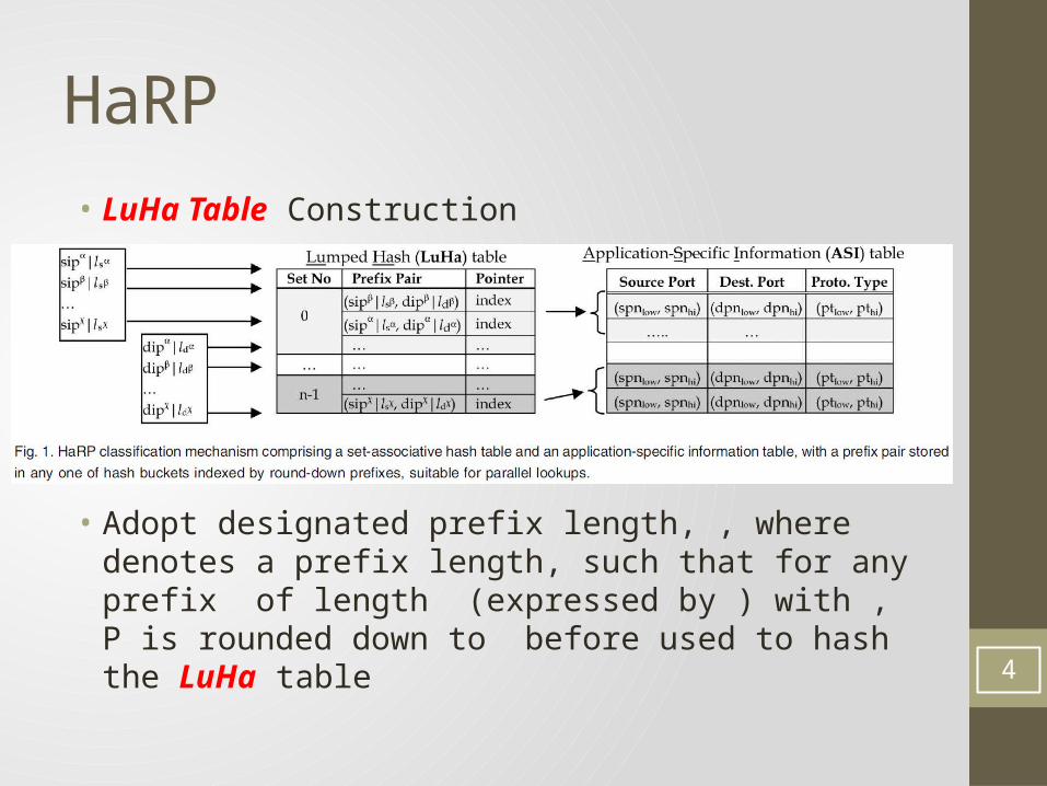
HaRP• LuHa Table Construction
• Adopt designated prefix length, , where denotes a prefix length, such that for any prefix of length (expressed by ) with , P is rounded down to before used to hash the LuHa table
4
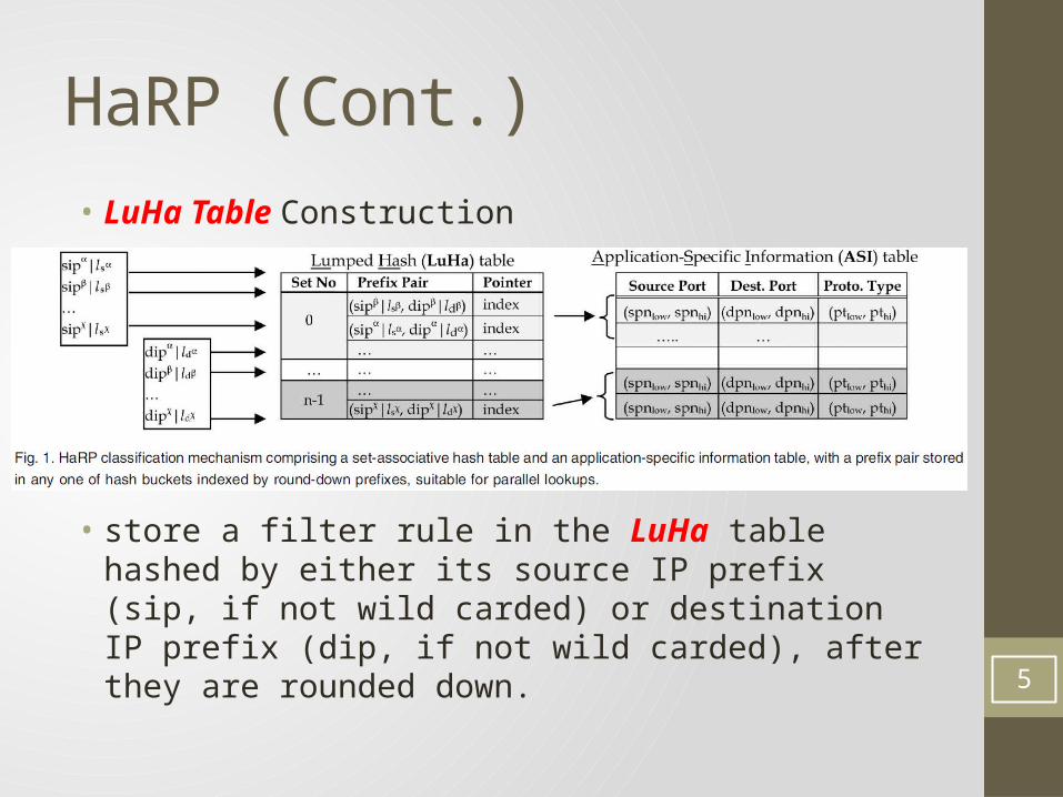
HaRP (Cont.)• LuHa Table Construction
• store a filter rule in the LuHa table hashed by either its source IP prefix (sip, if not wild carded) or destination IP prefix (dip, if not wild carded), after they are rounded down.
5
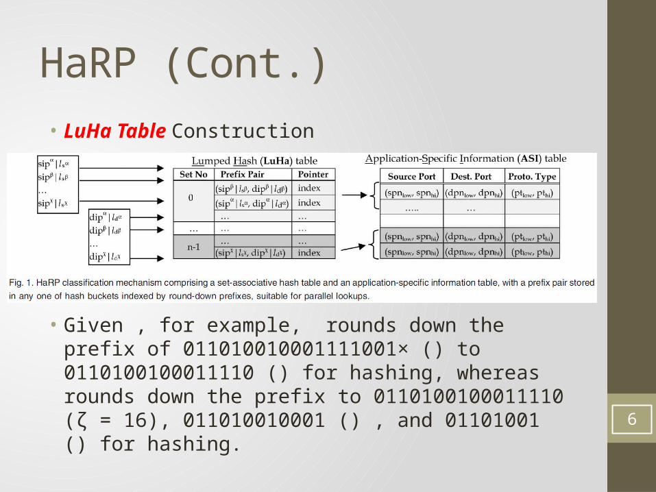
HaRP (Cont.)• LuHa Table Construction
• Given , for example, rounds down the prefix of 011010010001111001× () to 0110100100011110 () for hashing, whereas rounds down the prefix to 0110100100011110 (ζ = 16), 011010010001 () , and 01101001 () for hashing. 6
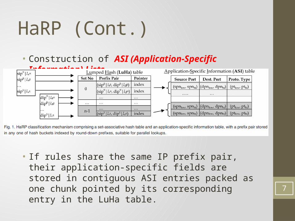
HaRP (Cont.)• Construction of ASI (Application-Specific Information) Lists
• If rules share the same IP prefix pair, their application-specific fields are stored in contiguous ASI entries packed as one chunk pointed by its corresponding entry in the LuHa table.
7

FPGA-based Design and Implementation• Layouts of Data Structures in Memory Blocks
• There are four major tables involved, the LuHa table, the PASI table, the SASI table, and the Pointer table.
8
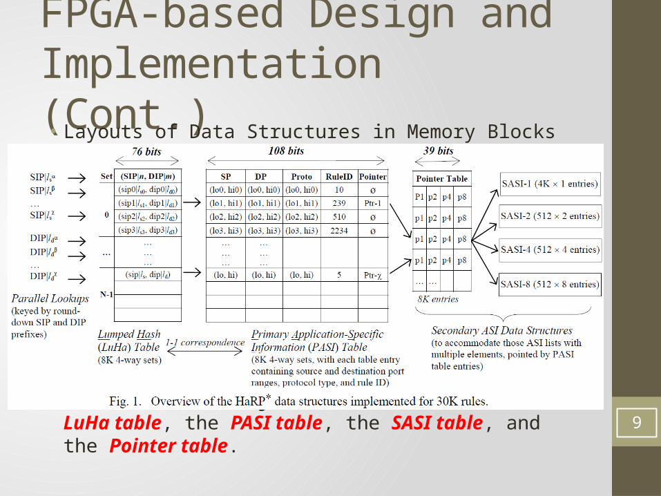
FPGA-based Design and Implementation (Cont.)• Layouts of Data Structures in Memory Blocks
• There are four major tables involved, the LuHa table, the PASI table, the SASI table, and the Pointer table.
9
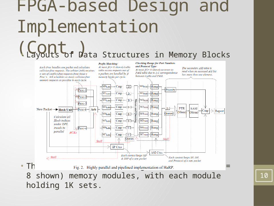
FPGA-based Design and Implementation (Cont.)• Layouts of Data Structures in Memory Blocks
• The LuHa table shown in Fig. 2 consists of (= 8 shown) memory modules, with each module holding 1K sets.
10

FPGA-based Design and Implementation (Cont.)• Layouts of Data Structures in Memory Blocks
• Each of the memory module is made to output 306 bits per read access, rendering four (SIP|n, DIP|m) pairs resided in one set of the 4-way LuHa table as depicted in Fig. 3.
11

FPGA-based Design and Implementation (Cont.)• Layouts of Data Structures in Memory Blocks
• The primary ASI (PASI) table has a 1-1 correspondence relationship to the LuHa table.
12

FPGA-based Design and Implementation (Cont.)• Layouts of Data Structures in Memory Blocks
• While the PASI table keeps the first element, the additional elements of an ASI entry are kept in the four secondary ASI component tables, which are referred to as the SASI table for simplicity.
13
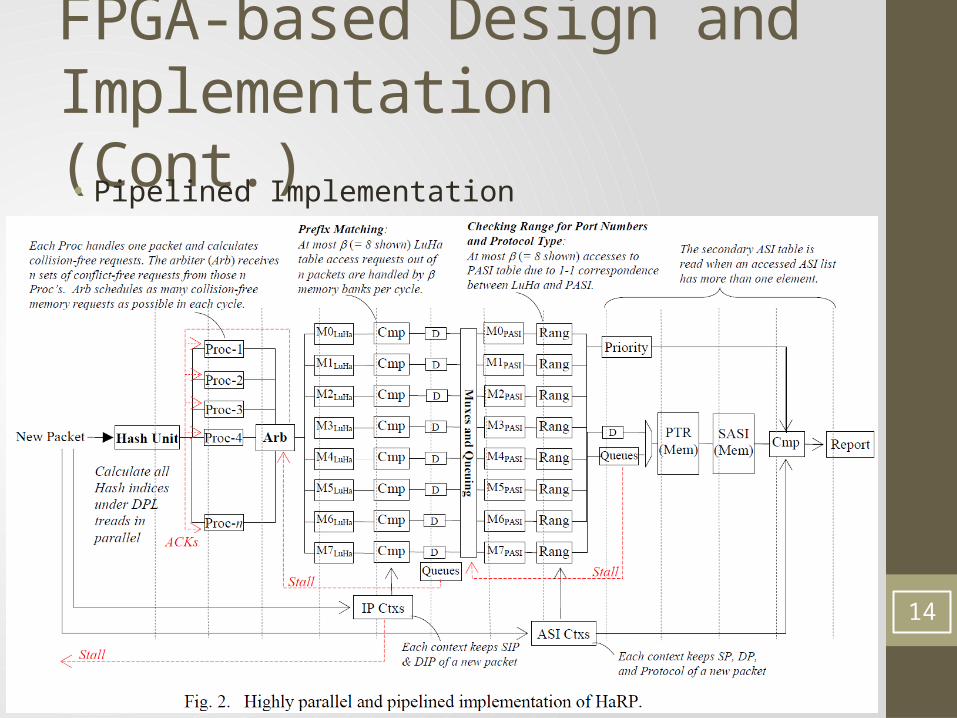
FPGA-based Design and Implementation (Cont.)• Pipelined Implementation
14
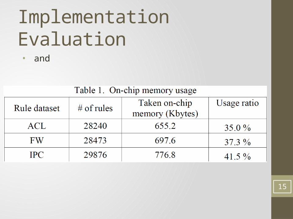
Implementation Evaluation• and
15
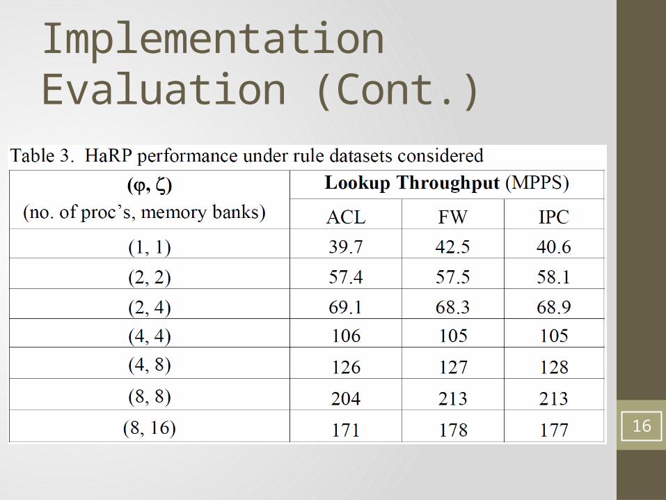
Implementation Evaluation (Cont.)
16
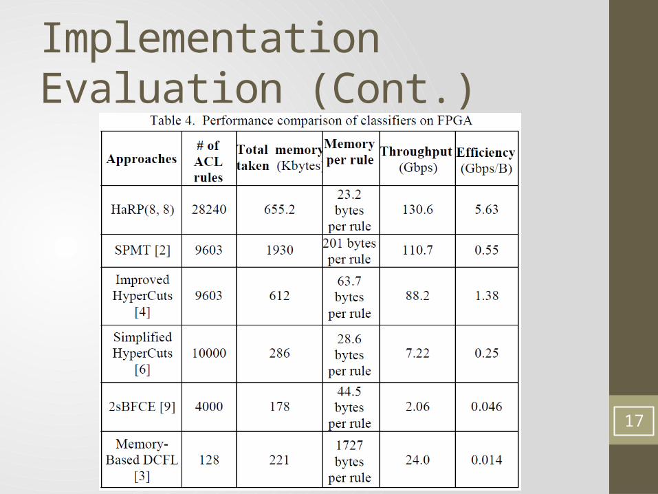
Implementation Evaluation (Cont.)
17