Embed Size (px)
Citation preview

UG028, November 24, 2015 1
Speedster22i SerDes User Guide
UG028 (v2.2) – November 24, 2015
2 UG028, November 24, 2015
Table of Contents
List of Figures .................................................................................................................................... 5
List of Tables ..................................................................................................................................... 6
Overview ............................................................................................................ 7
Physical Media Attachment (PMA) ..................................................................................................... 7
Clocking ............................................................................................................................................. 8
Physical Coding Sublayer (PCS)........................................................................................................ 8
Debug and Test ................................................................................................................................. 8
Major standards supported ................................................................................................................ 9
SerDes Placement ........................................................................................................................... 11
SerDes Architecture Overview ......................................................................................................... 12
Physical Media Attachment (PMA) ................................................................. 13
1. Common .................................................................................................................................. 13
2. Receiver (RX)/Transmitter (TX) ................................................................................................ 14
3. Digital PMA (DPMA) ................................................................................................................. 14
PCS Blocks in the Transmitter (TX) ............................................................... 16
PCS Self Test Logic ......................................................................................................................... 16
Polarity bit reversal (PBR) #0 and #1 ............................................................................................... 16 Polarity and Bit Inversion – 10/20 bit Operation ............................................................................................. 17 Polarity and Bit Inversion – 8/16 bit Operation ............................................................................................... 18
Interface Encapsulation ................................................................................................................... 20
8b/10b Encoder ............................................................................................................................... 20 Symbols and Comma Character ..................................................................................................................... 20
Running Disparity ............................................................................................................................ 20
PCS Blocks in the Receiver (RX) .................................................................... 22
Transition Density Checker (TDC) ................................................................................................... 22
Polarity Bit Reversal (PBR) .............................................................................................................. 23
Symbol Alignment ............................................................................................................................ 23 Modes of Operation ........................................................................................................................................ 24
Deskew FIFO ................................................................................................................................... 25 Functional Description .................................................................................................................................... 26
Lane-to-Lane Deskew Modes of Operation ...................................................................................... 26
UG028, November 24, 2015 3
The deskew module can work in three modes: .............................................................................................. 26 Standards Supported by Deskew Module ...................................................................................................... 27
Elastic FIFO (Elastic Buffer) ............................................................................................................. 27 EFIFO Standards and Skip Characters .......................................................................................................... 28 EFIFO Operation ............................................................................................................................................. 29 Overflow/Underflow ......................................................................................................................................... 31
8b/10b Decoder ............................................................................................................................... 31
Bit Slider .......................................................................................................................................... 31
Interface Encapsulation ................................................................................................................... 32
PCS Self Test Checker .................................................................................................................... 32
PCS Interface ................................................................................................... 33
Gigabit Ethernet Interface ................................................................................................................ 33
XAUI ................................................................................................................................................ 34
PIPE Interface .................................................................................................................................. 34
Clocking ........................................................................................................... 36
Debug and Test ............................................................................................... 38
Loopback Modes ............................................................................................................................. 38 PMA loopback modes: .................................................................................................................................... 39 PCS loopback modes: .................................................................................................................................... 39
PMA Test Pattern Generator ............................................................................................................ 39
PMA Test Pattern Checker .............................................................................................................. 40
PCS Test Pattern Generator ............................................................................................................ 40
PRBS Generator .............................................................................................................................. 40
PCS Test Pattern Checker ............................................................................................................... 41
Latency............................................................................................................. 42
PMA Latency ................................................................................................................................... 42
PCS Latency .................................................................................................................................... 42
Configurations Supported .............................................................................. 45
Design Flow: Creating a SerDes Design ........................................................ 49
Generating SerDes Wrapper using ACE GUI ................................................................................... 49
Single-Lane Serdes Wrapper ........................................................................................................... 50 Overview Section: ........................................................................................................................................... 53 Section on PMA Settings: ............................................................................................................................... 57 RX PMA Equalization ...................................................................................................................................... 59 RX PMA PLL ................................................................................................................................................... 60 TX PMA Driver ................................................................................................................................................ 62 TX PMA PLL ................................................................................................................................................... 62 Section on PCS Settings: ................................................................................................................................ 63
4 UG028, November 24, 2015
RX PCS Settings ............................................................................................................................................. 64 RX PCS Symbol Alignment ............................................................................................................................. 66 TX PCS Settings ............................................................................................................................................. 68 Section on Manually Overriding PMA/PCS Register Values: ......................................................................... 69 Generation of Wrapper Files: .......................................................................................................................... 70
Files Generated by ACE-GUI ........................................................................................................... 71
Integration of SerDes Wrapper in a Design ...................................................................................... 72 Design and Wrapper Files .............................................................................................................................. 72 Dynamically Changing the SerDes Register Values....................................................................................... 75 Using sBus module to enable internal loopback ............................................................................................. 75
Placement of SerDes ....................................................................................................................... 77 Timing Constraints .......................................................................................................................................... 78 Test bench Setup for Simulation ..................................................................................................................... 79
Design Guidelines ............................................................................................................................ 80 Reset Sequence ............................................................................................................................................. 80 SerDes Placement and Clocking Limitations .................................................................................................. 83 Wide Bus ......................................................................................................................................................... 88 Design Tips ..................................................................................................................................................... 89
Variants of the Simple Design .......................................................................................................... 90 Design Bypassing PCS: .................................................................................................................................. 95 Bypassing PCS by Manually Overriding Corresponding Register .................................................................. 97
Dynamic Read/Write of SerDes Registers via SBUS .................................. 100
Overview ........................................................................................................................................ 100 Alternatives for using SBUS interface for SerDes register access: .............................................................. 100
ACX_SERDES_SBUS_IF Module ................................................................................................. 101 The Ports of ACX_SERDES_SBUS_IF Module: .......................................................................................... 102 Loopback Modes ........................................................................................................................................... 104
SerDes Registers ........................................................................................... 105
Electrical Specifications ............................................................................... 106
Operating Conditions ..................................................................................................................... 106
Transmitter .................................................................................................................................... 107
Receiver ........................................................................................................................................ 110 Eye Diagram ................................................................................................................................................. 112
Reference Clock ............................................................................................................................ 113 Jitter Specification ......................................................................................................................................... 114
Revision History ............................................................................................ 115
UG028, November 24, 2015 5
List of Figures
Figure 1: Location of SerDes Lanes ...................................................................................................................................... 11 Figure 2: SerDes Architecture................................................................................................................................................ 12 Figure 3: PMA Architecture .................................................................................................................................................. 13 Figure 4: Synthesizer Architecture ....................................................................................................................................... 14 Figure 5: Receiver Architecture ............................................................................................................................................. 15 Figure 6: PCS Transmitter Block Overview ......................................................................................................................... 16 Figure 7: 20 bit Order Reversal ............................................................................................................................................. 17 Figure 8: 20-bit Byte Order Swap/Reversal ......................................................................................................................... 17 Figure 9: Polarity Inversion (16-bit Word) .......................................................................................................................... 18 Figure 10: Bit Order Inversion (16-bit Word) ...................................................................................................................... 18 Figure 11: Word Order Inversion (16-bit Word) ................................................................................................................. 19 Figure 12: 8b/10b Encoding Process ..................................................................................................................................... 21 Figure 13: PCS Receive Block Overview .............................................................................................................................. 22 Figure 14: Operating principle of deskew technique ......................................................................................................... 25 Figure 15: EFIFO SKP Addition/Removal ........................................................................................................................... 29 Figure 16: EFIFO SKP Addition/Removal: PCIE, GigE (802.3) and XAUI (802.3) ......................................................... 30 Figure 17: SerDes RX and TX clocks ..................................................................................................................................... 36 Figure 18: PMA Loopback Modes ........................................................................................................................................ 39 Figure 19: PCS Loopback Modes .......................................................................................................................................... 39 Figure 20: Worst-case latency across PMA and PCS (in terms of clock-cycles) ............................................................. 44 Figure 21: Opening IP Configuration Perspective .............................................................................................................. 50 Figure 22: New IP Configuration Window ......................................................................................................................... 51 Figure 23: New IP Configuration Window- Overview Page ............................................................................................ 52 Figure 24: Outline Window ................................................................................................................................................... 52 Figure 25: IP Diagran Window ............................................................................................................................................. 52 Figure 26: New IP Configuration Window – Populating Overview Page ...................................................................... 53 Figure 27: Issues with Setting TX/RX data rate and reference clock frequency ............................................................. 56 Figure 28: Unavailable Fields ................................................................................................................................................ 57 Figure 29: PMA Settings Window – First page ................................................................................................................... 58 Figure 30: Outline Window, When Lane-Specific PMA Settings are Enabled ............................................................... 59 Figure 31: PCS Settings Window – First page ..................................................................................................................... 63 Figure 32: PCS Settings for Receiver – Default Settings .................................................................................................... 64 Figure 33: PCS Settings for Receiver – Symbol Alignment ............................................................................................... 66 Figure 34: PCS Settings for Receiver – TX PCS Settings .................................................................................................... 68 Figure 35: Generating the Wrapper Files ............................................................................................................................. 70 Figure 36: TCL console message upon successful generation of wrapper files .............................................................. 71 Figure 37: Timing Requirements for Reset Signals ............................................................................................................ 80 Figure 38: Clock Region View ............................................................................................................................................... 84 Figure 39: Physical assignment of SerDes Lanes ................................................................................................................ 86 Figure 40: SerDes Placement Guidelines ............................................................................................................................. 87 Figure 41: PCS Settings for Receiver – Configurations for Decoder and Elastic FIFO .................................................. 93 Figure 42: Disabling PCS from ACE GUI ............................................................................................................................ 97 Figure 43: Modifying Register Settings from ACE GUI .................................................................................................... 98 Figure 44: Changing Value of Register 17A to bypass PCS block .................................................................................... 99 Figure 45: Disabling PCS Decoder (default ACE Setting) ............................................................................................... 101 Figure 46: Connections for ACX_SERDES_LOOPBACK_CTRL .................................................................................... 103 Figure 47: Receiver (RX) Eye Diagram Specification ....................................................................................................... 112
6 UG028, November 24, 2015
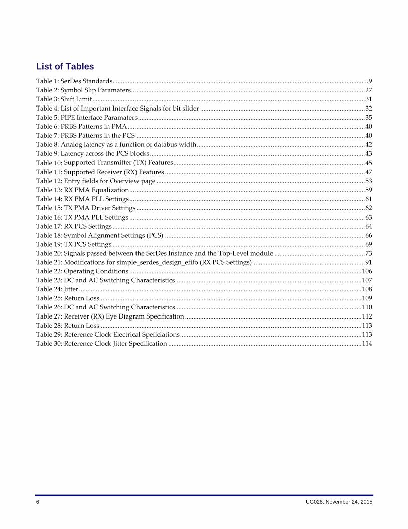
List of Tables
Table 1: SerDes Standards........................................................................................................................................................ 9 Table 2: Symbol Slip Paramaters........................................................................................................................................... 27 Table 3: Shift Limit .................................................................................................................................................................. 31 Table 4: List of Important Interface Signals for bit slider .................................................................................................. 32 Table 5: PIPE Interface Paramaters ....................................................................................................................................... 35 Table 6: PRBS Patterns in PMA ............................................................................................................................................. 40 Table 7: PRBS Patterns in the PCS ........................................................................................................................................ 40 Table 8: Analog latency as a function of databus width .................................................................................................... 42 Table 9: Latency across the PCS blocks ................................................................................................................................ 43
Table 10: Supported Transmitter (TX) Features .................................................................................................................. 45 Table 11: Supported Receiver (RX) Features ....................................................................................................................... 47 Table 12: Entry fields for Overview page ............................................................................................................................ 53 Table 13: RX PMA Equalization ............................................................................................................................................ 59 Table 14: RX PMA PLL Settings ............................................................................................................................................ 61 Table 15: TX PMA Driver Settings ........................................................................................................................................ 62 Table 16: TX PMA PLL Settings ............................................................................................................................................ 63 Table 17: RX PCS Settings ...................................................................................................................................................... 64 Table 18: Symbol Alignment Settings (PCS) ....................................................................................................................... 66 Table 19: TX PCS Settings ...................................................................................................................................................... 69 Table 20: Signals passed between the SerDes Instance and the Top-Level module ...................................................... 73 Table 21: Modifications for simple_serdes_design_efifo (RX PCS Settings)................................................................... 91 Table 22: Operating Conditions .......................................................................................................................................... 106 Table 23: DC and AC Switching Characteristics .............................................................................................................. 107 Table 24: Jitter ........................................................................................................................................................................ 108 Table 25: Return Loss ........................................................................................................................................................... 109 Table 26: DC and AC Switching Characteristics .............................................................................................................. 110 Table 27: Receiver (RX) Eye Diagram Specification ......................................................................................................... 112 Table 28: Return Loss ........................................................................................................................................................... 113 Table 29: Reference Clock Electrical Speficiations ............................................................................................................ 113 Table 30: Reference Clock Jitter Specification ................................................................................................................... 114
UG028, November 24, 2015 7
Chapter 1 – SerDes Architecture
Overview
Achronix Speedster22i FPGAs provide very high core fabric and I/O performance which exceeds the system bandwidth requirements of various high end applications. The Speedster22i device family supports up to 64 full-duplex SerDes lanes, each supporting up to 11.3 Gbps data rate.
The Physical Coding Sublayer (PCS) and Physical Media Attachment (PMA) sub-blocks together comprise a single SerDes block. The SerDes PCS has explicit support for PCIe, 10GBASE-R, 1G Ethernet and XAUI. It also has some support for various other interconnect protocols through PCS such as Interlaken, SPI4.2, Infiniband, Fiber-Channel, SAS/SATA, SONET, OC, OBSAI and CPRI. The SerDes can be connected either to the embedded Hard-IPs (PCIe, Interlaken, and 10/40/100G MAC) or to the FPGA Fabric for soft implementation of any other protocol supported.
Physical Media Attachment (PMA)
Data rates supported
o 1.0625 – 11.3 Gbps
o 531.25 – 1062.5 Mbps using 2X over-sampling
o 265.625 – 531.25 Mbps using 4X over-sampling
Independent lane architecture with dedicated synthesizer for each lane with no off-chip components required
Low power architecture (<100mW at 10Gbps)
Support both AC and DC coupling
Input driver with Continuous Time Linear Equalizer (CTLE) and Decision Feedback Equalizer (DFE)
o Input voltage: 50 – 2000 mVp-p differential
o Auto-calibrating CTLE and DFE
o CTLE with up to 20dB gain tuned for key data rates
o Pulse-shaped 5-tap DFE
Output driver with 4-tap Finite Input Response (FIR) filter with Feed Forward Equalizer (FFE)
o Output voltage: 400 – 1500 mVp-p differential
o Slew rate: 31 – 170 ps
Highly digital PLL architecture for the Synthesizer and CDR
o Accuracy & low jitter of an analog PLL
o Tuning range of a digital PLL
8 UG028, November 24, 2015
o Programmable spread spectrum generation
o Support for 16-bit fractional multiplication factors
o Programmable spread spectrum clocking
o Support for fast lock mode for EPON/GPON
On-chip scope in the receiver for measuring eye width, eye height and BER for the incoming signal
On-chip calibrated 100 ohm termination
Transparent calibration engine to compensate for PVT variation
Clocking
Support for external reference clock from 50 MHz – 300 MHz
Support for recovered reference clock for loop timing and re-timer type applications that eliminates the need for a cleanup PLL
Physical Coding Sublayer (PCS)
Bypassable and Modular PCS architecture
Support for 8b/10b and 128b/130b encoding
Symbol alignment
Clock and phase compensation FIFO
Lane to lane de-skew
Polarity inversion
Bit reversal
Lane bonding
Low/Deterministic latency modes for protocols such as CPRI and OBSAI
Debug and Test
Up to seven different near-end and far-end loopback modes in PMA and PCS
Built-in self test (BIST)
o PRBS 7, 15, 23, 31 and 40-bit user defined pattern generators and checkers in the PCS
o PRBS 7, 23, 31 and 40-bit user defined pattern generators and checkers in the PMA

UG028, November 24, 2015 9
Major standards supported
Table 1: SerDes Standards
Standards Variation Data Rate(s)
PCI Express
Gen1 2.5 Gbps
Gen 2 5.0 Gbps
Gen 3 8.0 Gbps
Gigabit Ethernet 1000BASE-CX 1.25 Gbps
SGMII 1.25 Gbps
10 Gigabit Ethernet
XAUI (802.3ae) 3.125 Gbps
XFI 10.3125 Gbps
SFI over SFP+ (SFF-8431) 10.3125 Gbps
10GBASE-R (802.3ae) 10.3125 Gbps
10GBase-KR
(802.3ae) 10.3125 Gbps
XLAUI/CAUI
(802.3ae) 10.3125 Gbps
Interlaken -- 3.125 – 10.3125 Gbps
OIF
SPI5 3.125 Gbps
SFI-4.2 3.125 Gbps
SFI-5.1 3.125 Gbps
SFI-5.2 9.1 – 10.3125 Gbps
SFI-S 11.1 Gbps
CEI 6G 4.976 – 6.375 Gbps
CEI 11G 9.95 – 11.2 Gbps
Fiber Channel
FC-1 1.0625 Gbps
FC-2 2.125 Gbps
FC-4 4.25 Gbps
FC-8 8.5 Gbps
FC-10 10.52 Gbps
SONET
OC-12 622.08 Mbps
OC-24 1244.16 Mbps
OC-48 2488.32 Mbps
OC-192 9953.28 Mbps

10 UG028, November 24, 2015
Standards Variation Data Rate(s)
QPI 4.8 Gbps
6.4 Gbps
SATA
SATA-1 1.5 Gbps
SATA-2 3.0 Gbps
SATA-3 6.0 Gbps
SAS
SAS-1 3.0 Gbps
SAS-2 6.0 Gbps
SAS-3 12.0 Gbps
Serial Rapid I/O
Gen1
Gen1
Gen1
Gen2
Gen2
1.25 Gbps
2.5 Gbps
3.125 Gbps
5.0 Gbps
6.125 Gbps
E-PON 802.3av
1.25 Gbps
2.5 Gbps
10 Gbps
GPON --
1.25 Gbps
2.5 Gbps
10 Gbps
InfiniBand
SDR
DDR
QDR
2.5 Gbps
5.0 Gbps
10.0 Gbps
JESD204B Up to 12.5 Gbps
CPRI -- 614.4 – 9830.4 Mbps
OBSAI -- 768 – 6144 Mbps
USB 3.0 5.0 Gbps
USB 3.1 10.0 Gbps
UG028, November 24, 2015 11
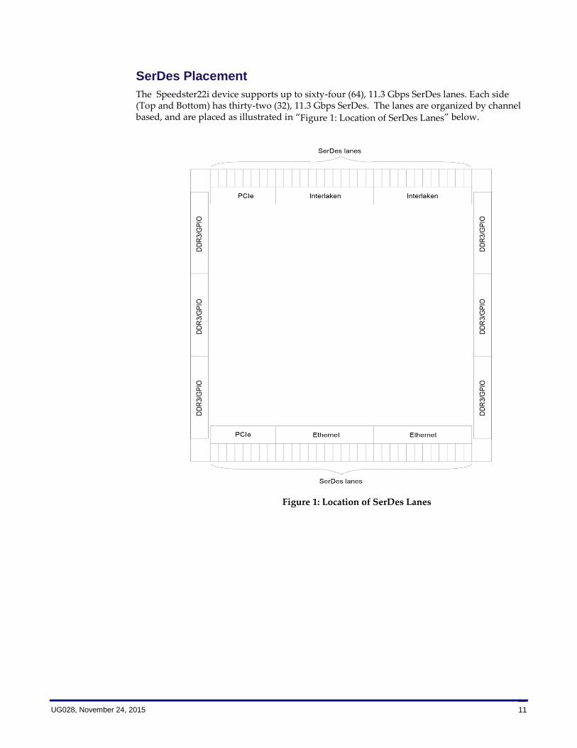
SerDes Placement
The Speedster22i device supports up to sixty-four (64), 11.3 Gbps SerDes lanes. Each side (Top and Bottom) has thirty-two (32), 11.3 Gbps SerDes. The lanes are organized by channel based, and are placed as illustrated in “Figure 1: Location of SerDes Lanes” below.
Figure 1: Location of SerDes Lanes
12 UG028, November 24, 2015
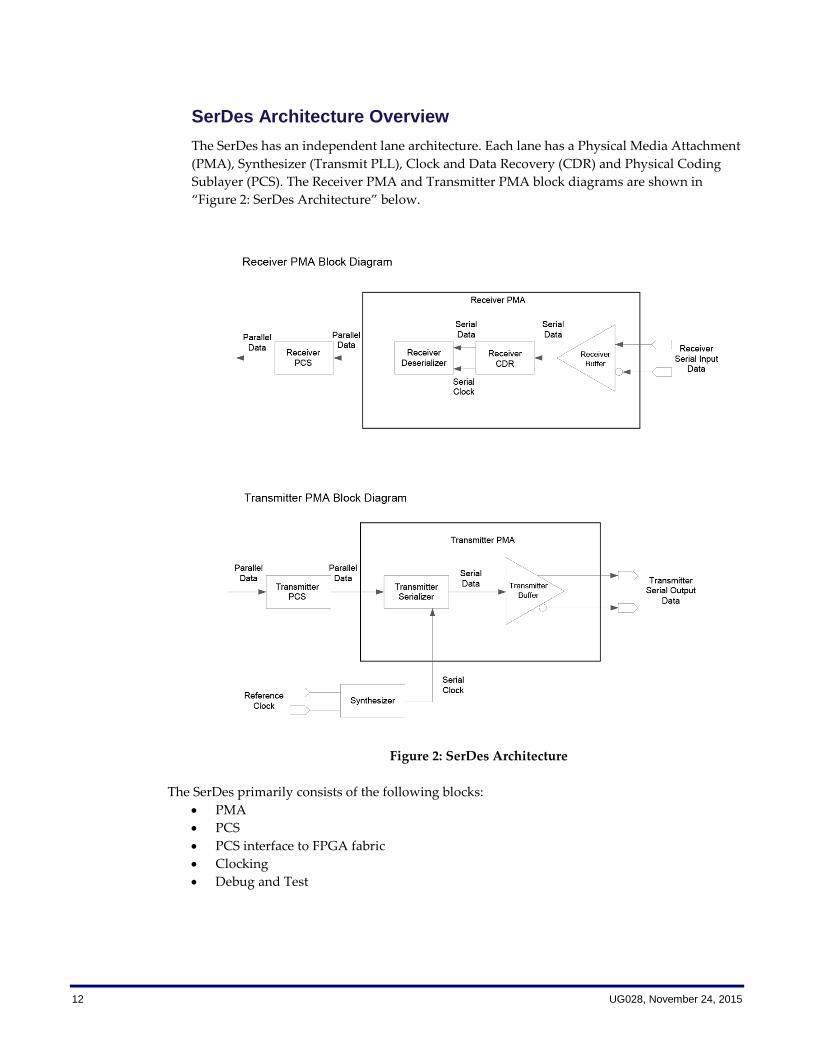
SerDes Architecture Overview
The SerDes has an independent lane architecture. Each lane has a Physical Media Attachment
(PMA), Synthesizer (Transmit PLL), Clock and Data Recovery (CDR) and Physical Coding
Sublayer (PCS). The Receiver PMA and Transmitter PMA block diagrams are shown in
“Figure 2: SerDes Architecture” below.
Figure 2: SerDes Architecture
The SerDes primarily consists of the following blocks:
PMA
PCS
PCS interface to FPGA fabric
Clocking
Debug and Test
UG028, November 24, 2015 13
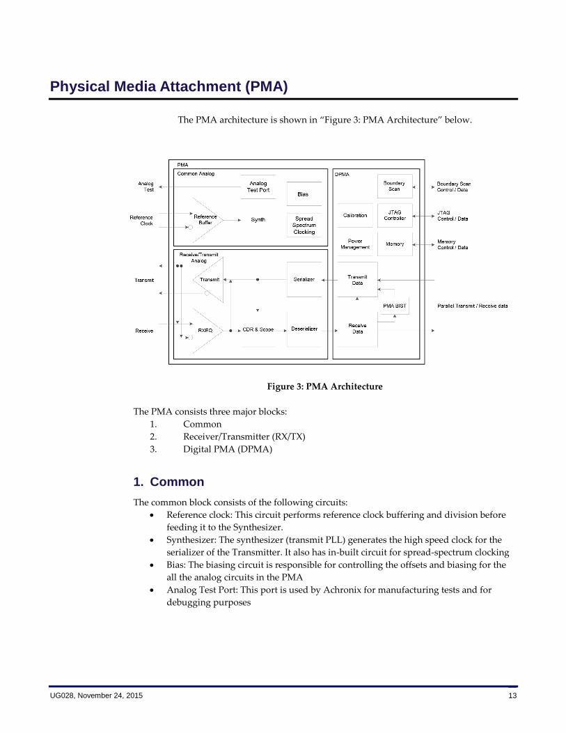
Physical Media Attachment (PMA)
The PMA architecture is shown in “Figure 3: PMA Architecture” below.
Figure 3: PMA Architecture
The PMA consists three major blocks:
1. Common
2. Receiver/Transmitter (RX/TX)
3. Digital PMA (DPMA)
1. Common
The common block consists of the following circuits:
Reference clock: This circuit performs reference clock buffering and division before
feeding it to the Synthesizer.
Synthesizer: The synthesizer (transmit PLL) generates the high speed clock for the
serializer of the Transmitter. It also has in-built circuit for spread-spectrum clocking
Bias: The biasing circuit is responsible for controlling the offsets and biasing for the
all the analog circuits in the PMA
Analog Test Port: This port is used by Achronix for manufacturing tests and for
debugging purposes

14 UG028, November 24, 2015
2. Receiver (RX)/Transmitter (TX)
The RX/TX block consists of the following circuits:
TX buffer: Converts single-ended signal to differential and performs equalization on
(or pre-emphasis) the outgoing serial signal
RX buffer: Converts differential signal to single ended and performs equalization on
incoming signal using Continuous Time Linear Equalizer (CTLE) and Decision
Feedback Equalizer (DFE)
Clock Data Recovery (CDR): Recovers clock and data from the incoming signal for
deserialization
On-Chip Scope: Used for plotting an eye of the incoming signal post equalization for
debug
Serializer/Deserializer: Converts parallel data to serial data using a high speed clock
from the synthesizer
3. Digital PMA (DPMA)
The DPMA block consists of the following circuits:
Calibration: Performs calibration of all the analog circuits using trim settings and
offsets
PMA BIST: Includes PRBS 7, 23, 31 and 40-bit user defined pattern generators and
checkers Power management
Configuration registers (Memory)
JTAG and Boundary Scan
Figure 4: Synthesizer Architecture

UG028, November 24, 2015 15
Figure 5: Receiver Architecture

16 UG028, November 24, 2015
PCS Blocks in the Transmitter (TX)
This section presents the transmitter (TX) data path within a PCS. The key blocks within the
SerDes transmitter are:
Encoder: Encodes the data for transmission line. Primary goal is to ensure DC
balance by eliminating long sequence of 1’s or 0’s.
Polarity Bit Reversal (PBR): Inverts the polarity of data and ordering of data to be
transmitted.
The building block for the SerDes IP is the 1 lane configuration. A simplified block diagram
of the TX data path is shown in Figure 6: PCS Transmitter Block Overview . The functional
blocks shown in the diagram represent the functionality supported by a single SerDes lane. A
summary of the supported standards is covered in “Table 1: SerDes Standards”.
Figure 6: PCS Transmitter Block Overview
* SerDes configured in Generic mode supports only 8b/10b encoding.
** Either of PBR#0 or PBR#1 can be used or both may be bypassed.
Note: The PCS block will support lane-bonding across multiple SerDes lanes (max 12) Chapter – “Design Flow: Creating a SerDes Design” presents the ground-up steps that can be followed to prepare a design that supports lane-bonding.
The PCS blocks on TX path are detailed below.
PCS Self Test Logic
This block generates transmit data for PCS self test, detailed in “PCS Test Pattern Generator” and “PCS Test Pattern Checker”.
Polarity bit reversal (PBR) #0 and #1
This block can invert the polarity of the incoming data. It can also reverse the bits of the incoming data such that effectively the most significant bit is sent first, rather than the least significant bit (default). For 16/20bit (2 words) bit streams, the word order can also be inverted such that effectively the most significant byte is sent first, rather than the least significant byte (default).
There are two PBR blocks on transmission data path, as shown in “Figure 6: PCS Transmitter Block Overview”. PBR0 is used before the protocol encapsulation block and PBR1 is used on encoded data. Either PBR0 or PBR1 can be used. Alternatively, both of these two blocks can be bypassed.

UG028, November 24, 2015 17
Polarity and Bit Inversion – 10/20 bit Operation
When operating in 10bit/20bit mode, the bit order within each 10-bit word can be inverted. This is illustrated in “Figure 7: 20 bit Order Reversal”. Effectively the most significant bit of the least significant byte is transmitted first (i.e. bit 9 of byte 0 is transmitted first).
Figure 7: 20 bit Order Reversal
When the word order is reversed in 20-bit mode, the most significant byte (byte 1) is swapped with the least significant byte (byte 0). This is illustrated in “Figure 8: 20-bit ”. The most significant byte will be transmitted first in such a case
Figure 8: 20-bit Byte Order Swap/Reversal
The polarity for the entire 10bit or 20bit word can be inverted as well. Polarity inversion applies to the entire word (10 bits or 20 bits).
18 UG028, November 24, 2015
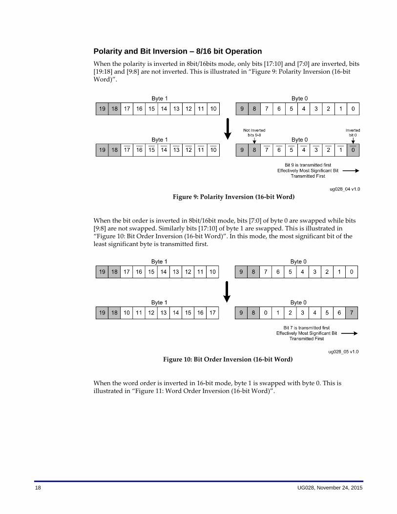
Polarity and Bit Inversion – 8/16 bit Operation
When the polarity is inverted in 8bit/16bits mode, only bits [17:10] and [7:0] are inverted, bits [19:18] and [9:8] are not inverted. This is illustrated in “Figure 9: Polarity Inversion (16-bit Word)”.
Figure 9: Polarity Inversion (16-bit Word)
When the bit order is inverted in 8bit/16bit mode, bits [7:0] of byte 0 are swapped while bits [9:8] are not swapped. Similarly bits [17:10] of byte 1 are swapped. This is illustrated in “Figure 10: Bit Order Inversion (16-bit Word)”. In this mode, the most significant bit of the least significant byte is transmitted first.
Figure 10: Bit Order Inversion (16-bit Word)
When the word order is inverted in 16-bit mode, byte 1 is swapped with byte 0. This is illustrated in “Figure 11: Word Order Inversion (16-bit Word)”.

UG028, November 24, 2015 19
Figure 11: Word Order Inversion (16-bit Word)

20 UG028, November 24, 2015
Interface Encapsulation
This block encapsulates the protocols supported by the SerDes in Achronix FPGA. The user may refer to Section – “PCS Interface” for details on the protocols supported. It may be noted again that the SerDes configured in Generic mode supports only 8b/10b encoding.
8b/10b Encoder
The 8b/10b encoder generates 10-bit code groups from 8-bit data and a 1-bit control input. It uses the code group mapping specified in IEEE 802.3 clause 36. If the fabric interface is a 16-bit data path, then two 8b/10b encoders are cascaded to produce a 20-bit code group output to the PMA for serialization.
The 8b/10b encoder essentially translates 8-bit words to 10-bit symbols. This encoding scheme has been proven to achieve DC-balance and running disparity while providing sufficient information for clock recovery. (See the later sections for more information on DC-Balance, running disparity and clock recovery.) The 10-bit encoded output TX_dataout[9:0] will map to bits {jhgf iedcba}per the labeling used in IEEE 802.3-2005 clause 36.
Symbols and Comma Character
While translating 8-bit words into 10-bit symbols, the 8b/10b encoder (in SerDes PCS) form two groups of data. The lower 5-bits of data are encoded into a 6-bit group and the upper 3-bits of data are encoded into a 4-bit group. Furthermore, there are 12 control symbols that are used by 8b/10b encoding scheme for special purposes and are called K-symbols. For instance three of these control symbols can be used for defining the boundary between data packets. These three control symbols are called comma symbols.
The 8b/10b encoder generates 10-bit code groups from 8-bit data and a 1-bit control input. It uses the code group mapping specified in IEEE 802.3 clause 36. If the fabric interface is a 16-bit data path, then two 8b/10b encoders are cascaded to produce a 20-bit code group output to the PMA for serialization. The 1-bit control input (datak signal) is used to identify whether data being transmitted is a comma symbol. Asserted value for datak signal on control-line indicates that the symbol on data-line is a comma symbol.
In Section-“Design and Wrapper Files” of the Chapter – “Design Flow: Creating a SerDes Design”, details are provided on how to transmit 8’hBC (K.28.5) as comma symbol and 1’b1 as control signal, for a sample design. For a 20-bit data width, that design essentially uses {2’h1, 8’hBC, 2’h1, 8’hBC}. In other words, while sending a comma symbol, TX_data[8:8] = TX_data[18:18] = 1’b1 is sent through the control-line.
Note: On the receiver end, when the decoder finds an ‘asserted’ control-bit on control-line, it will consider the symbol on data-line as a comma symbol. Error conditions occur if the datak signal is asserted while there is no comma symbol on the data line (e.g. K21.5).
Running Disparity
A non-encoded data stream may have differences between the number of 1’s and the number of 0’s. The primary goal of using running disparity in the encoding scheme is to limit the difference between the number of 1’s and the number of 0’s that are being transmitted. This ensures DC balance on the transmission line. A side-benefit of using running disparity is that information from running disparity can be used in locating transmission errors. This ensures that the output data is DC balanced. The maximum run length for 8b/10b words is 5 bits.

UG028, November 24, 2015 21
The input disparity for the 6 bit block is based on the disparity of previous word’s 4 bit block while the disparity for the 4 bit block is the disparity of the current word’s 6 bit block. This is illustrated in “Figure 12: 8b/10b Encoding Process”.
Figure 12: 8b/10b Encoding Process
22 UG028, November 24, 2015
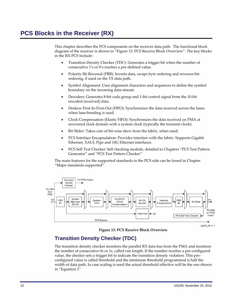
PCS Blocks in the Receiver (RX)
This chapter describes the PCS components on the receiver data path. The functional block diagram of the receiver is shown in “Figure 13: PCS Receive Block Overview”. The key blocks in the RX-PCS include:
Transition Density Checker (TDC): Generates a trigger bit when the number of consecutive 1’s or 0’s reaches a pre-defined value.
Polarity Bit Reversal (PBR): Inverts data, swaps byte ordering and reverses bit-ordering, if used on the TX data path.
Symbol Alignment: Uses alignment characters and sequences to define the symbol boundary on the incoming data-stream.
Decoders: Generates 8-bit code group and 1-bit control signal from the 10-bit encoded (received) data.
Deskew First-In-First-Out (FIFO): Synchronizes the data received across the lanes when lane-bonding is used.
Clock Compensation (Elastic FIFO): Synchronizes the data received on PMA at recovered clock domain with a system clock (typically the transmit clock).
Bit Slider: Takes care of bit-wise skew from the fabric, when used.
PCS Interface Encapsulation: Provides interface with the fabric. Supports Gigabit Ethernet, XAUI, Pipe and 10G Ethernet interfaces.
PCS Self Test Checker: Self checking module, detailed in Chapters “PCS Test Pattern Generator” and “PCS Test Pattern Checker”
The main features for the supported standards in the PCS side can be found in Chapter “Major standards supported”
Figure 13: PCS Receive Block Overview
Transition Density Checker (TDC)
The transition density checker monitors the parallel RX data bus from the PMA and monitors the number of consecutive 0s or 1s, called run length. If the number reaches a pre-configured value, the checker sets a trigger bit to indicate the transition density violation. This pre-configured value is called threshold and the minimum threshold programmed is half the width of data path. In case scaling is used the actual threshold effective will be the one shown in “Equation 1”

UG028, November 24, 2015 23
Equation 1:
The assert signal from Transition Density Checker can be taken to fabric.
Note: Any bit transition would cause the counter to clear and the count to restart.
Polarity Bit Reversal (PBR)
The polarity bit reversal block is used to invert data, swap byte ordering, and reverse bit-ordering. There are two such PCS blocks on the receive path, corresponding to the two polarity bit reversal blocks on the transmit path.
When the polarity bit reversal on transmit path is performed before protocol encapsulation (PBR #0 on “Figure 6: PCS Transmitter Block Overview”), the PBR block after protocol encapsulation is used on receive path (PBR #0 on “Figure 13: PCS Receive Block Overview”). In contrast, if PBR operation is performed on encoded data on the transmit path (PBR #1 on “Figure 6: PCS Transmitter Block Overview”), the PBR block before symbol alignment/decoder block is used on the receive path (PBR #1 on “Figure 13: PCS Receive Block Overview”). As noted earlier, both of these blocks can be disabled, both on the transmit and the receive paths.
Symbol Alignment
Symbol alignment uses alignment and sequence characters for identifying the correct symbol boundary in the received data-stream. Attributes for alignment and sequence detect symbols are specified to be 10-bit wide. But when received data-path is in 8-bit (or 16-bit) wide mode, only the lower 8-bits of attribute will be considered.
The symbol alignment block can be configured to support a variety of standards. Some of these standards are listed below:
• PCIe
• XAUI
• GigE
• Infiniband
• Serial Rapid IO
• SPI-5 (lock to training pattern)
• CPRI
• OBSAI
• Fiber Channel
Symbol alignment can be programmed to function in the following modes:
• Manual Mode
• Bit slip Mode
• Automatic Mode

24 UG028, November 24, 2015
Modes of Operation
Manual Mode:
In manual alignment mode, the symbol alignment will attempt to identify a pre-configured pattern and lock to the incoming de-serialized data-stream from the output of the PMA or phase picking block. The alignment operation is triggered by the user logic in the FPGA on the rising edge of RX_com_det_en. The symbol alignment block then searches for the pre-configured alignment pattern with or without trailing sequence pattern. Fabric will wait for the lock status. Once lock to the incoming stream is achieved, the fabric can monitor error status from the 8b/10b decoder or employ any other mechanism in fabric to identify loss of lock. The Fabric asserts another rising edge to trigger a new alignment cycle.
Bit Slip Mode:
In bit slip mode, the user logic controls the symbol alignment using the RX_bit_slip_en signal. Each rising edge of RX_bit_slip_en causes the symbol alignment logic to shift the word boundary by 1-bit, and symbol alignment will attempt to match the alignment pattern within the new word boundary. If the word boundary is not matched, the user logic can again assert RX_bit_slip_en, possibly after waiting for a timeout causing the word boundary to shift by another bit position. This loop continues until lock is achieved. Once lock to the incoming stream is achieved, logic in the fabric can monitor error status from 8b/10b decoder or employ some other mechanism in fabric to identify loss of lock. The bit slip mode supports all attributes used for manual alignment mode. The maximum number of slips that will cause a true change in alignment is limited to the data path width.
Automatic Mode:
In automatic alignment mode, the symbol alignment block will automatically determine the location of the word boundary based on the pre-configured alignment characters. It will also establish a lock acquired condition based on receiving a pre-con d count of alignment characters (hysteresis). A loss of lock condition also can be detected by this block based on a pre-configured count of bad code words (or alignment characters at a different word boundary). Instead of counting every bad code word, the user can decide to count every ‘n’ bad code word for an incrementing unlock count. Also, the user can use decode/disparity errors as per clause 36 of IEEE 802.3 to increment and decrement the unlock counter. Support for Fiber Channel protocol involves synchronization with the 4-symbol wide transmission word (a special code word K28.5 followed by 3 data code words). In case of Fiber Channel, any malformed transmission word causes the symbol alignment to go out of lock based on the un-lock count programmed.
Comma symbols are used for identifying the correct symbol boundary. Section – “Symbols and Comma Character” introduces comma symbols and discusses on how they are used in data output from 8b/10b encoder on the TX side of a SerDes. At the receiver end, the incoming data is scanned for comma symbols. Once the comma symbol is found, the deserializer resets the word boundary of the received data. The received data is continuously scanned for the subsequent comma symbols.

UG028, November 24, 2015 25
Deskew FIFO
The deskew block provides support for standards which require multiple lane bonding and de-skewing of received data across multiple lanes. Lane bonding is required when the users want to transmit data faster than is possible by using one serial link (lane). In such case, the data is received must be aligned across the lanes. Deskew module within the SerDes takes care of this.
Figure 14: Operating principle of deskew technique
“Figure 14: Operating principle of deskew technique” shows the operating principle of deskew operation. In this figure, data is being sent using four lanes. On the receiver side, before lane-bonding, we find that the data at time t+2on lane-1 is aligned with data at time t+1 on lane-2 and so on. The deskew technique aims to align the data with respect to the clock cycles. In other words, data at time t+2on lane-2 should be aligned with data at time t+2 on the other lanes. The red lines for the clock at receiver end demonstrates this.
For lane bonding, all lanes should use the same reference clock and insert de-skew characters at the same time on each lane. Skew between lanes is introduced by both active (CDR) and passive (board) elements of the link. The deskew operation can result in some loss of data when it aligns characters to the same clock cycle.

26 UG028, November 24, 2015
Functional Description
The de-skew block uses a deskew FIFO on each lane. The writes to the deskew FIFO are performed in the recovered clock domain for each lane. The read side of the deskew FIFO is clocked by the clock from the initiator lane. The lanes are categorized as initiator and followers. Any lane can be an initiator and skew is always calculated between the initiator and each of follower lanes.
Once deskew is enabled, the skew between initiator and follower lanes are calculated continuously by sensing deskew characters in the read side of the FIFO. The read threshold for the FIFO needs to be programmed appropriately based on skew tolerance to avoid FIFO under/over run. Once a deskew character is sensed, each lane starts a skew window equal to the maximum skew allowed in the system. Based on how the lanes are skewed, the follower lane is either lagging or leading and adjust the read clock cycles accordingly. Once the initiator gets indication from all lanes of the bonding group that the skew calculation is over, it declares that all lanes are aligned and asserts data valid for the down-stream logic. The same data valid is used by the follower lanes to assert respective lane data valid. When the initiator does not find such overlap of skew windows, it issues a reset to all FIFOs in the bonding group and restarts the de-skew operation.
To summarize, the initiator lane generates various control signals for the follower lanes and follower lanes send various status signals back to the initiators. Status signals are AND-ed (e.g. for checking if the skew calculation completed in all lanes) or OR-ed (e.g. for checking if any follower lanes window has not started), whereas control signals are used directly. These signals go from one lane to another. The status and control signals are registered at time intervals determined based on the number of lanes bonded
Lane-to-Lane Deskew Modes of Operation
The deskew module can work in three modes:
Manual Mode:
The rising edge of i_dskew_start will start one round of deskew operation. Lanes are declared aligned either just after the deskew operation is completed or after an additional check of a programmed number of aligned deskew characters in all bonded lanes at the same time. The fabric needs to monitor received data for identifying any misalignment, and thus to restart deskew operation. Infiniband uses manual mode of deskew operation.
Auto Mode:
The deskew module is always active. Once lanes are deskewed, all lanes will continuously look for deskew characters in data read from the FIFO. The initiator should see deskew characters on all lanes of the bonding group at the same time. The initiator looks for aligned deskew characters on all lanes for a certain number of times based on the value programmed in the register, and once detected the initiator declares bonded lanes aligned. Any time the initiator finds deskew characters not aligned on all lanes, it starts an unlock count. If the unlock count hits the value programmed in the register, the initiator declares that the lanes are out of lock and re-starts the de-skew operation. While unlock count is incrementing, if the initiator finds de-skew characters are aligned on all lanes again it starts decrementing the unlock counter. This decrement can happen once in every ‘n’ (programmed in the register) times when lanes have de-skew characters aligned to make sure the link has overcome error conditions. If the unlock counter reaches zero, the link remains aligned.

UG028, November 24, 2015 27
Symbol slip mode:
The deskew module does not actively remove skew across lanes. Each lane is controlled by the fabric. Fabric continuously monitors incoming data and employ a mechanism to find out the skew across lanes. Based on the calculation, it instructs each lane to adjust the read pointer of FIFO. The read pointer can be incremented once by 0, 1 or 2 based on the combination of rising edges on symbol_slip_up and symbol_slip_dn. Based on the skew computed, the fabric may need to provide multiple transitions on symbol_slip_up and symbol_slip_dn to get the required number of pointer adjustments.
Table 2: Symbol Slip Paramaters
symbol_slip_up symbol_slip_dn Comments
0 0 Increment read pointer by 1
0 1 No increment
1 0 Increment read pointer by 2
1 1 Increment read pointer by 1
Standards Supported by Deskew Module
The deskew module in Achronix SerDes has explicit support for XAUI and Infiniband. For XAUI, align(||A||) characters are sent periodically as per section 48 in IEEE 802.3. For Infiniband, training sequences (TS1/TS2) are used as deskew characters. Though each of TS1/TS2 is 16 code words long, the de-skew module forms de-skew ordered set with COM and four data symbols (D10.2). The distance (gap) between COM and data symbols should be programmed to ‘d1 for Infiniband. In case of 10-bit data path, the max skew handled is 6-bytes and for 20-bit max skew handled 2-bytes. For training in Infiniband, initially data valid will be asserted to pass TS1/TS2/TS3 to fabric. Subsequently, data valid is removed when link training is completed and the fabric decides to de-skew lanes bonded. Once the de-skew operation is completed, data valid is asserted again.
Besides these two protocols, the user can use this module for deskew functions of any protocols provided that the minimum spacing between de-skew characters are maintained.
Elastic FIFO (Elastic Buffer)
An elastic FIFO is used to synchronize the received data from the PMA recovered clock to a system clock, typically the transmit clock. The Elastic FIFO also compensates for any frequency offset between the recovered clock and the system clock. It compensates for the frequency offset by adding or deleting pre-configured skip (or pad) characters from the received data stream. The elastic FIFO in Achronix SerDes provides an indication that skip (or pad) characters were added or deleted to the downstream logic. For PCIe, the elastic FIFO also includes the appropriate status encoding to indicate add/delete operation.
The elastic FIFO can also be configured to be used as a simple phase compensation FIFO for synchronizing data. When used as a phase compensation FIFO, it is left to the user to guarantee that there is no frequency offset (jitter) between the read and write clocks.

28 UG028, November 24, 2015
EFIFO Standards and Skip Characters
PCIe Gen3: To support PCIe Gen3, 4-bytes of skip are added at byte positions 4-7 from the sync header associated with the skip ordered set. Skip removal happens from bytes 0-3 from the sync header associated with the skip ordered set. Due to this particular rule of removal, sync header and receive start block indications are delayed by 4-bytes.
PCIe Gen1/Gen2: For PCIe Gen1/Gen2, the skip ordered set is two 10-bit words – the elastic buffer adds or deletes only the second word.
Fiber Channel: To support Fiber channel, 4-bytes of skip are added and deleted. The PCS operates in 16-bit data-path mode at the fabric interface and 20-bit encoding internally.
XAUI: To support XAUI, the skip ordered set is one 10-bit word, which is added or deleted by the elastic buffer.
GigE: For GigE, the skip ordered set is two 10-bit words – control followed by data. The elastic FIFO adds or removes both of these two 10-bit words.
Other Standards: Besides these specific standards, the elastic FIFO can handle any generic protocols in the similar line due to the programmable nature of SKIP and inverted SKIP ordered set of length 2. The user has flexibility to include an alternate (mostly inverted) word in the ordered set. Beyond two words skip ordered sets, only 4 words skip ordered sets can be used, which are specific to fiber channel. The elastic FIFO generates the final data valid from the PCS, which is used by the fabric to register data.

UG028, November 24, 2015 29
EFIFO Operation
“Figure 15: EFIFO SKP Addition/Removal” illustrates the process of SKP addition/removal.
Figure 15: EFIFO SKP Addition/Removal
In “Figure 15: EFIFO SKP Addition/Removal” upon reset, the difference between the read and write counters is equal to fifo_mid (half the size of the buffer; default 16).
If clk_in is operating at a lower frequency than clk_out, then the read operation is faster than the write operation and the difference between the write and read counters will be less than fifo_mid. In this case, to compensate for clk_in being slower, an SKP is added to the data stream.
If clk_in is operating at a higher frequency than clk_out, then the read operation is slower than the write operation and the difference between the write and read counters will be greater than fifo_mid. In this case, to compensate for clk_out being slower, an SKP is removed from the data stream.
30 UG028, November 24, 2015
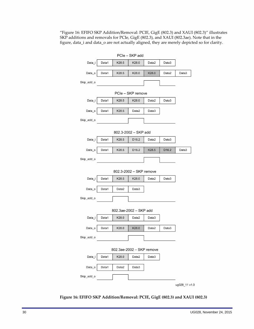
“Figure 16: EFIFO SKP Addition/Removal: PCIE, GigE (802.3) and XAUI (802.3)” illustrates SKP additions and removals for PCIe, GigE (802.3), and XAUI (802.3ae). Note that in the figure, data_i and data_o are not actually aligned, they are merely depicted so for clarity.
Figure 16: EFIFO SKP Addition/Removal: PCIE, GigE (802.3) and XAUI (802.3)
UG028, November 24, 2015 31
Overflow/Underflow
If the difference between the write and read counters is greater than fifo_full, then the overflow signal is asserted. If the difference between the write and read counters is less than fifo_empty, then the underflow signal is asserted.
8b/10b Decoder
The 8b/10b decoder generates 8-bit code groups and 1-bit control from 10-bit encoded (received) data. It uses the code group mapping specified in IEEE 802.3 clause 36. If the fabric interface is a 16-bit data path, then two 8b/10b decoders are cascaded to produce 16-bit data to the fabric. The decoder handles various error conditions. All error conditions are reported per each byte lane.
The 8b/10b code allows 12 special (K) characters, but most standards generally support fewer K characters and need the reserved K characters to be declared as code errors. So register programming is possible to pre-configure 11 characters that can be declared as invalid for deciding code error if seen in the receive data stream, and assuming that at least one special character will be needed.
Any 10-bit code word that is not present in Tables 36-1, 36-2 of the IEEE 802.3-2005 specification shall be considered as invalid code word. In addition, 11 code words corresponding to the K characters can be included (programmable) to be flagged as invalid code words. If the 10-bit code word is present in Tables 36-1 or 36-2, but corresponds to the wrong column (per current running disparity calculation), the wrong column indication is asserted. Disparity and code errors are not mutually exclusive; however code error and wrong column are mutually exclusive.
For XAUI and Gigabit Ethernet, a code error or disparity error will cause the error indication to be propagated downstream. For PCIe, if a code error and disparity error are detected on the same byte, the pipe_RXstatus is encoded to indicate a code error.
Bit Slider
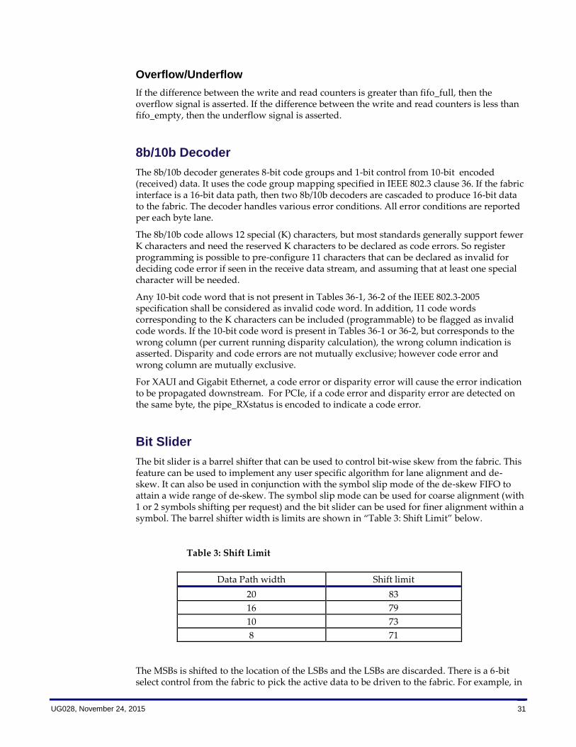
The bit slider is a barrel shifter that can be used to control bit-wise skew from the fabric. This feature can be used to implement any user specific algorithm for lane alignment and de-skew. It can also be used in conjunction with the symbol slip mode of the de-skew FIFO to attain a wide range of de-skew. The symbol slip mode can be used for coarse alignment (with 1 or 2 symbols shifting per request) and the bit slider can be used for finer alignment within a symbol. The barrel shifter width is limits are shown in “Table 3: Shift Limit” below.
Table 3: Shift Limit
Data Path width Shift limit
20 83
16 79
10 73
8 71
The MSBs is shifted to the location of the LSBs and the LSBs are discarded. There is a 6-bit select control from the fabric to pick the active data to be driven to the fabric. For example, in
32 UG028, November 24, 2015
the 20-bit mode of operation, the most significant 20-bits of data are placed on bits 19:0 of the barrel shifter and the least significant 20-bits are discarded. The 6-bit select control can select a range of active bits, from [19:0] (for a select value of 0x00) to [82:63] (for a select value of 0x3F).
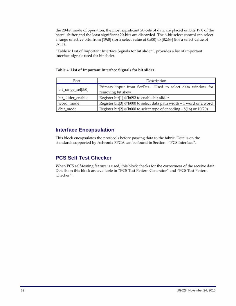
“Table 4: List of Important Interface Signals for bit slider”, provides a list of important interface signals used for bit slider.
Table 4: List of Important Interface Signals for bit slider
Port Description
bit_range_sel[5:0] Primary input from SerDes. Used to select data window for
removing bit skew
bit_slider_enable Register bit[1] @’h092 to enable bit-slider
word_mode Register bit[3] @’h000 to select data path width – 1 word or 2 word
8bit_mode Register bit[2] @’h000 to select type of encoding - 8(16) or 10(20)
Interface Encapsulation
This block encapsulates the protocols before passing data to the fabric. Details on the standards supported by Achronix FPGA can be found in Section –“PCS Interface”.
PCS Self Test Checker
When PCS self-testing feature is used, this block checks for the correctness of the receive data. Details on this block are available in “PCS Test Pattern Generator” and “PCS Test Pattern Checker”.
UG028, November 24, 2015 33
PCS Interface
The PCS interface provides the general interface between the PCS and the core fabric. The PCS supports the following interfaces:
• Gigabit Ethernet Interface
• XAUI
• PIPE Interface
• 10G Ethernet Interface
Gigabit Ethernet Interface
The PCS in Achronix SerDes supports 10G Ethernet, compliant with section 36, 37 of IEEE 802.3. Functionalities implemented are PCS transmit, carrier sense, synchronization, receive, and auto-negotiation.
The PCS transmit process is facilitated at both the GMII and PMA interfaces to the PCS. At the GMII interface (fabric side), the PCS uses 8-bit synchronous data-path with packet de-limiting, done by separate transmit control (TX_en, TX_err) and receive control signals (RX_dv, RX_err). At the PMA interface, the PCS uses 10-bit data path, which uses 10-bit code groups. Besides generating 10-bit code groups continuously based on GMII signals (TXd[7:0], TX_dv, TX_err), transmit process also generates GMII signal col if reception is concurrent with transmit. The transmit process also monitors auto-negotiation to determine whether it needs to send data or reconfigure the link. As part of transmit process, the state machines shown in Figures 36-15 and 36-16 of IEEE 802.3 are implemented. To enable carrier sense the PCS generates an internal flag.
The PCS Synchronization process determines whether the PMA is functioning reliably. The PCS Synchronization process continuously accepts code-groups and conveys received code-groups to the PCS Receive process. For synchronization, a symbol alignment module is used. For synchronization, the state machines shown in Figures 36-9 of IEEE 802.3 are implemented.
The PCS Receive process continuously accepts code-groups. The PCS Receive process monitors these code-groups and generates RXD <7:0>, RX_DV, and RX_ER on the GMII, and the internal flag used by the Carrier Sense and Transmit processes. For synchronization, the state machines shown in Figures 36-7 of IEEE 802.3 are implemented.
The PCS Auto-Negotiation process sets the xmit flag to inform the PCS Transmit process to either transmit idles interspersed with packets as requested by the GMII or to reconfigure the link. The PCS auto-negotiation process is specified in the state machine shown in Figure 37-6 of IEEE 802.3. As part of auto-negotiation, the PCS will advertise only as a 1G link full-duplex partner. The following management registers are currently implemented:
a. Control register (Register 0)
b. Status register (Register 1)
c. AN advertisement register (Register 4)
d. AN link partner ability base page register (Register 5)
These management registers are accessible through SBUS i/f (P1). A MDIO-to-SBUS bridge can be implemented in the fabric. The reset duration of these controllers is programmable via register, and the max duration is defined as 0.5sec as per IEEE 802.3.
34 UG028, November 24, 2015
XAUI
The PCS supports XAUI compliant with section 48 of IEEE 802.3. The Protocol block implements the Transmit and Receive state machines as per Figures 48-6 and 48-9 of IEEE 802.3. For synchronization, de-skew and clock compensation operations, symbol alignment, de-skew and elastic buffers in PCS are used. 8b/10b encoders and decoders are used for handling 10-bit code groups.
When communicating with the XGMII (fabric side), the PCS uses in each direction 32 data signals and 4 control signals. When communicating with the PMA, the PCS uses a 40-bit code-group in the transmit direction and in the receive direction. Each set of 40-bit data signals conveys four lanes of 10-bit code-groups. The 40-bit code-group signals are organized into four lanes: the first PCS code-group is aligned to lane 0, the second to lane 1, the third to lane 2, and the fourth to lane 3. Code-group alignment, lane-to-lane de-skew, and provision for clock rate compensation are made possible by embedding special non-data code-groups in the idle stream.
The PCS Transmit process continuously generates code-groups based upon the TXd [31:0] and TXc [3:0] signals on the XGMII, sending them to the PMA service interface.
The PCS Synchronization process indicates whether the PMA is functioning dependably, which can be determined without exhaustive error-rate analysis. The PCS Synchronization process continuously accepts unaligned and unsynchronized code-groups from the PMA, obtains 10-bit code-group synchronization, and conveys synchronized 10-bit code-groups to the PCS de-skew process as per Figure 48-7 in IEEE 802.3.
The PCS de-skew process continuously accepts synchronized code-groups, aligns the code-groups to remove skew between the lanes introduced by the link, and conveys aligned and synchronized code-groups to the PCS Receive process. At the end of the de-skew process, the PCS will have successfully de-skewed and aligned code-groups on all PCS lanes. The de-skew process always looks for non-aligned code-groups across 4-lanes and initiates de-skew operations as per Figure 48-6 in IEEE 802.3.
Clock rate compensation is required when the received clock from the PMA and the clock on which data is sent to fabric are different in terms of jitter. The PCS compensates by inserting or deleting SKIP (||R||) characters in the encoded idle stream. Insertion and deletion is only done after SKIP (||R||) is detected – not arbitrarily on any positions.
The Receive process operates in two modes as per Figure 48-9 in IEEE 802.3: date and idle mode. In data mode, valid code-groups received are mapped to corresponding XGMII data or control characters regardless of whether the control characters are valid XGMII control characters. Invalid or error code-groups are mapped directly to XGMII Error control characters. In idle mode, an idle code-group is translated to XGMII Idle control characters. All code-groups are mapped on a lane by lane basis.
PIPE Interface
The PCS supports the PIPE interface compliant to the Intel PIPE 3.0 specification. It supports a 10/20-bit data path for gen1/gen2 and 16-bit for gen3. Similarly, it supports 2.5G, 5.0G and 8.0G throughput on the PMA. For gen1/gen2, 8b/10b endec and gen3 128b/130b endec are used. This interface allows the embedded PCIe MAC to configure the PMA and decide upon the next course of action based on the status sent out by the PMA. Besides the functions described in the PIPE interface specifications, it facilitates the MAC in setting up the receive equalizer in the PMA. When the PCS is supporting PCIe/PIPE, lane de-skew is done by the MAC and clock compensation is done by the elastic buffer in the PCS.
The PCS also supports a 128b/130b encoder, specifically targeted for PCIe gen3 (based on draft 0.5 of the PCIe 3.0 specification). The interface is compliant to the PIPE 3.0 specification.
UG028, November 24, 2015 35
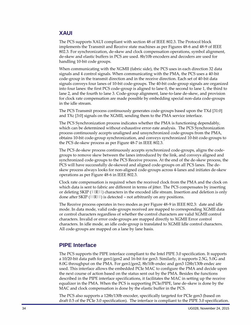
The 128b/130b encoder is disabled on power up, and enabled when the rate bits coming from the MAC are configured to 2’b10. The PCS layer support for PCIe gen3 also includes glue logic to switch the PMA data width to 16-bit mode and programming final rate bits for PCIe gen3 operation. “Table 5: PIPE Interface Paramaters” shows various supported combinations of clocking speeds and data-widths.
Table 5: PIPE Interface Paramaters
PCIe Mode PCLK PMA Data Width
2.5 Gbps Gen1 250 Mhz 10 bits
2.5 Gbps Gen1 125 Mhz 20 bits
5.0 Gbps Gen2 500 Mhz 10 bits
5.0 Gbps Gen2 250 Mhz 20 bits
8.0 Gbps Gen3 500 Mhz 16 bits
36 UG028, November 24, 2015
Clocking
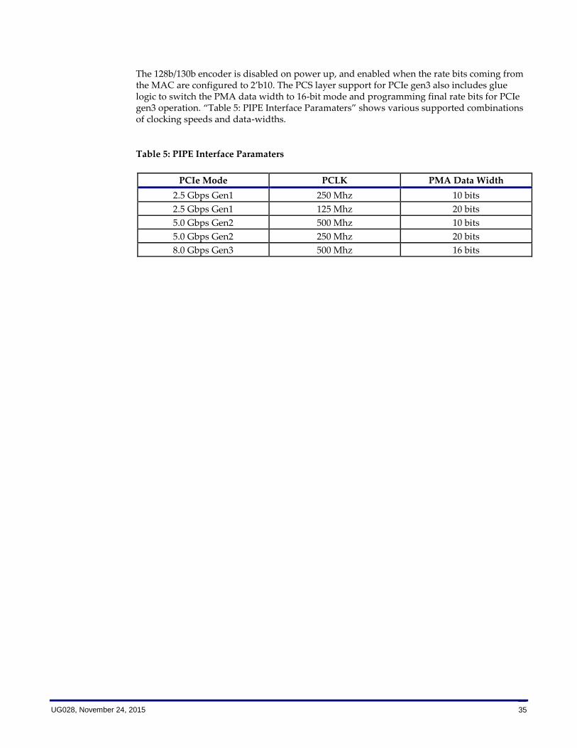
“Figure 17: SerDes RX and TX clocks” gives an overview of the clocks inside the SerDes. The PMA of a SerDes lane generates two clocks, a TX word clock synthesized from the reference clock, and an RX word clock recovered from the incoming serial data stream. The frequency of these clocks is the data rate divided by the word width. For instance, a 10Gbps data rate with 20 bit data width results in a 500MHz clock. Since the TX and RX clocks are generated separately, they must be designated as unrelated in the timing constraints. In the most basic mode, these TX and RX clocks are used to clock the data in their respective directions, and are brought into the FPGA fabric for use by the user design.
Because each SerDes lane has its own PMA to generate a TX clock and an RX clock, the clocks of different lanes are unrelated to each other, and consequently there is no synchronization between the data of different lanes. Some protocols distribute data over a group of SerDes lanes to increase bandwidth; typically, the lanes in such a group must then be synchronized to give the appearance of a single high-bandwidth data stream. To synchronize multiple SerDes lanes, Lane Bonding is used. As the Figure illustrates, when Lane Bonding is enabled, a single lane is designated as master, and its TX and RX clocks are used to clock all the lanes in the group. The deskew FIFO is used to convert data from the recovered clock domain to the master RX domain; see Section “Deskew FIFO” for more details.
Figure 17: SerDes RX and TX clocks

UG028, November 24, 2015 37
Although each lane has its own clock output pins to the fabric, with lane bonding these are all just route-throughs of the master clock: regardless of which clock output pins are used, only one clock net is routed inside the fabric. This is an important feature of Lane Bonding, because the FPGA fabric can only accommodate a limited number of distinct clocks. Lane Bonding divides the number of distinct clocks inside the core by the size of the group. Note that Lane Bonding is only possible when all lanes share the same reference clock, both at the near end and at the far end.
An additional method of reducing the number of distinct clocks is to use the Elastic FIFO. That FIFO can be used to convert data from the RX domain to the TX domain, thus reducing the number of distinct clocks by half. In Elastic FIFO mode, the RX clock output to the fabric is just a route-through of the TX clock: either clock pin can be used, and only a single net will be routed inside the fabric. See Section “Elastic FIFO” for details of Elastic Buffer operation.
Elastic FIFO mode and Lane Bonding mode can be combined, reducing the number of clocks to one for the entire bonded group.
As mentioned above, a 10Gbps data rate results in a 500MHz clock output to the user design (or 625MHz for 16 bit words). For most designs, timing closure at such high clock speeds is unrealistic. Because of that, the SerDes macro includes a “Wide Bus” feature, which divides the clock frequency by two and doubles the data width. When the Wide Bus feature is enabled, the TX and RX clock outputs from the macro to the user design are the divided clocks, and the user design does not need to deal with the faster clock at all. However, because the Wide Bus is implemented in the fabric, both the fast and divided clocks do occur in the fabric, counting towards the maximum number of distinct clocks. The Wide Bus feature can be combined with Lane Bonding and Elastic FIFO modes. See the Section “Design Guidelines” for specifics on the number of distinct clocks that the fabric can support, and for details of the Wide Bus feature.
38 UG028, November 24, 2015
Debug and Test
The SerDes comes integrated with a wide range of debug and test features for excellent coverage. The following features are provided:
Seven different loopback modes
Pseudo-Random Binary Sequence (PRBS) pattern generators and checkers on PMA and PCS.
User-defined pattern generator and checker in PMA and PCS.
Loopback Modes
The SerDes supports up to seven different loopback modes. The loopback modes can be divided as PMA loopback and PCS loopback. Each of the PMA and PCS loopbacks has Near end and Far-end loopback. Near End loopback loops back the data from transmit side to the receive side while Far end loopback, loops back data from receive side to the transmit side.
1. PMA loopback mode
A. Near End
(i) TX to RX PMA Serial internal loopback – This loopback is serial transmit to receive buffered loopback. Loops back the TX serializer output into the CDR bypassing the IO drivers.
B. Far End
(ii) RX to TX PMA serial loopback - Transmits the untimed, partial equalized RX serial data on the transmit IO pins.
(iii) RX to TX PMA parallel loopback – Loops back 20 bit receive data port to 20 bit transmit data port. This uses synthesized bit clock for transmit.
(iv) RX to TX PMA parallel loopback using recovered clock (Loop timing mode) - Loops back 20 bit receive data port to 20 bit transmit data port. This uses recovered clock (CDR) for transmit.
2. PCS loopback mode
A. Near End
(i) TX to RX PCS parallel loopback – Transmit data is looped back on the receive path at the PMA interface.
B. Far End
(ii) RX to TX PCS parallel loopback – Receive data is looped back on the transmit side at the fabric interface. This uses synthesized bit clock for transmit.
(iii) RX to TX PCS parallel loopback using recovered clock - Receive data is looped back on the transmit side at the fabric interface. This uses recovered clock (CDR) for transmit.
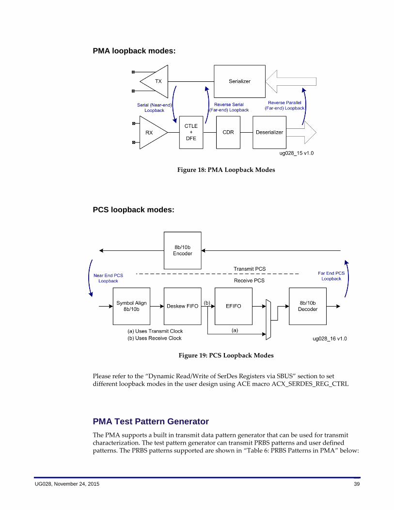
UG028, November 24, 2015 39
PMA loopback modes:
Figure 18: PMA Loopback Modes
PCS loopback modes:
Figure 19: PCS Loopback Modes
Please refer to the “Dynamic Read/Write of SerDes Registers via SBUS” section to set different loopback modes in the user design using ACE macro ACX_SERDES_REG_CTRL
PMA Test Pattern Generator
The PMA supports a built in transmit data pattern generator that can be used for transmit characterization. The test pattern generator can transmit PRBS patterns and user defined patterns. The PRBS patterns supported are shown in “Table 6: PRBS Patterns in PMA” below:

40 UG028, November 24, 2015
Table 6: PRBS Patterns in PMA
Bus Width PRBS Pattern Available
PRBS-7 1+x6+x7
PRBS-23 1+x18+x23
PRBS-31 1+x28+x31
The transmit pattern generator can generate user defined pattern by configuring control registers. The user defined pattern can be a 40 bit memory pattern.
PMA Test Pattern Checker
The PMA Test pattern checker on the receive data path can be used to check all the standard data patterns and user defined patterns by enabling the self test checker. The standard data patterns include the PRBS patterns as described in Table above. The user defined pattern is a 40-bit memory pattern checker. The PRBS transmitter and receiver are enabled by selecting the loopback modes described in section “Dynamic Read/Write of SerDes Registers via SBUS”.
PCS Test Pattern Generator
The PCS can be programmed to transmit test pattern data instead of user provided transmit data coming from fabric interface. The test pattern generator is used to check the quality of the serial link and supports various standard patterns. The test pattern generator can transmit PRBS patterns and user defined patterns. The PRBS patterns currently supported are shown in “Table 7: PRBS Patterns in the PCS”.
PRBS Generator
Various PRBS patterns can be generated by the transmit block which are summarized in “Table 7: PRBS Patterns in the PCS”.
Table 7: PRBS Patterns in the PCS
Bus Width PRBS Pattern Available
PRBS-7 1+x6+x7
PRBS-15 1+x14+x15.
PRBS-20 1+x3+x20
PRBS-23 1+x18+x23
PRBS-31 1+x28+x31
The transmit pattern generator can optionally transmit user defined patterns instead of PRBS patterns, configured through the control registers. Two sets of user defined patterns (up to 40-bits each) can be configured. The user can decide to send a single 40-bit pattern or two alternate 40-bit patterns.
The transmit test pattern generation supports two modes of operation -
Non-framed transmit mode
Framed transmit mode
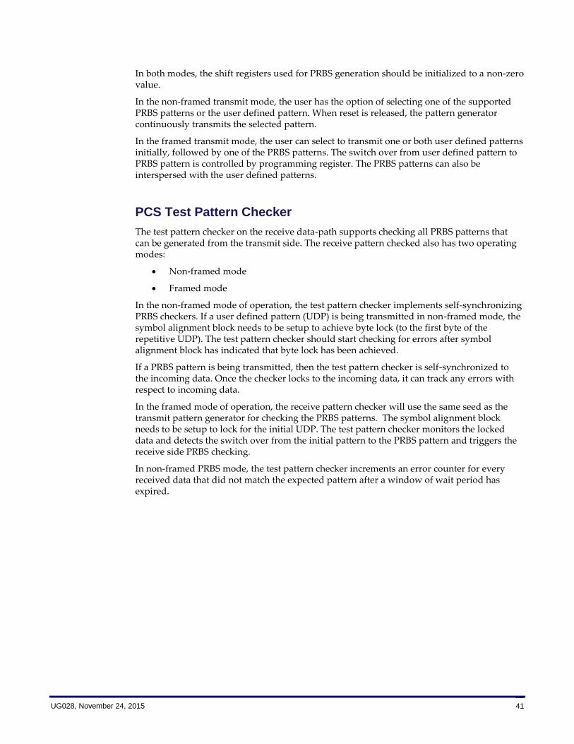
UG028, November 24, 2015 41
In both modes, the shift registers used for PRBS generation should be initialized to a non-zero value.
In the non-framed transmit mode, the user has the option of selecting one of the supported PRBS patterns or the user defined pattern. When reset is released, the pattern generator continuously transmits the selected pattern.
In the framed transmit mode, the user can select to transmit one or both user defined patterns initially, followed by one of the PRBS patterns. The switch over from user defined pattern to PRBS pattern is controlled by programming register. The PRBS patterns can also be interspersed with the user defined patterns.
PCS Test Pattern Checker
The test pattern checker on the receive data-path supports checking all PRBS patterns that can be generated from the transmit side. The receive pattern checked also has two operating modes:
Non-framed mode
Framed mode
In the non-framed mode of operation, the test pattern checker implements self-synchronizing PRBS checkers. If a user defined pattern (UDP) is being transmitted in non-framed mode, the symbol alignment block needs to be setup to achieve byte lock (to the first byte of the repetitive UDP). The test pattern checker should start checking for errors after symbol alignment block has indicated that byte lock has been achieved.
If a PRBS pattern is being transmitted, then the test pattern checker is self-synchronized to the incoming data. Once the checker locks to the incoming data, it can track any errors with respect to incoming data.
In the framed mode of operation, the receive pattern checker will use the same seed as the transmit pattern generator for checking the PRBS patterns. The symbol alignment block needs to be setup to lock for the initial UDP. The test pattern checker monitors the locked data and detects the switch over from the initial pattern to the PRBS pattern and triggers the receive side PRBS checking.
In non-framed PRBS mode, the test pattern checker increments an error counter for every received data that did not match the expected pattern after a window of wait period has expired.
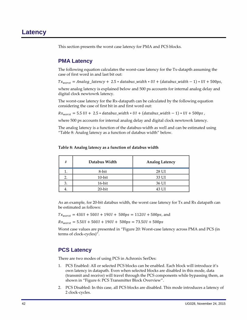
42 UG028, November 24, 2015
Latency
This section presents the worst case latency for PMA and PCS blocks.
PMA Latency
The following equation calculates the worst-case latency for the Tx-datapth assuming the case of first word in and last bit out:
_ ,
where analog latency is explained below and 500 ps accounts for internal analog delay and digital clock newtowrk latency.
The worst-case latency for the Rx-datapath can be calculated by the following equation considering the case of first bit in and first word out:
,
where 500 ps accounts for internal analog delay and digital clock newtowrk latency.
The analog latency is a function of the databus-width as well and can be estimated using “Table 8: Analog latency as a function of databus width” below.
Table 8: Analog latency as a function of databus width
# Databus Width Analog Latency
1. 8-bit 28 UI
2. 10-bit 33 UI
3. 16-bit 36 UI
4. 20-bit 43 UI
As an example, for 20-bit databus width, the worst case latency for Tx and Rx datapath can be estimated as follows:
, and
Worst case values are presented in “Figure 20: Worst-case latency across PMA and PCS (in terms of clock-cycles)”.
PCS Latency
There are two modes of using PCS in Achronix SerDes:
1. PCS Enabled: All or selected PCS blocks can be enabled. Each block will introduce it’s own latency in datapath. Even when selected blocks are disabled in this mode, data (transmit and receive) will travel through the PCS components while bypassing them, as shown in “Figure 6: PCS Transmitter Block Overview”.
2. PCS Disabled: In this case, all PCS blocks are disabled. This mode introduces a latency of 2 clock-cycles.

UG028, November 24, 2015 43
“Table 9: Latency across the PCS blocks” presents the latency experienced by datapath in these two modes. The worst case latency is presented in in “Figure 20: Worst-case latency across PMA and PCS”
Table 9: Latency across the PCS blocks
# PCS Module Data Path Latency experienced by datapath
PCS Enabled PCS Bypassed
1. Polarity bit reversal
symbol swap 0 Transmit 0 Not applicable
2. 8b/10b Encoder Transmit 2 Not applicable
3. Polarity bit reversal
symbol swap 1 Receive 0 Not applicable
4. 8b/10b Decoder Receive 2 Not applicable
5. Symbol Alignment
Module Receive 2 Not applicable
6. Deskew Module Receive FIFO_Threshold + 5 Not applicable
7. EFIFO Module Receive FIFO threshold + 7 +
no_of_lanes_bonded/4* Not applicable
8. Other 2
Total Latency 13 (max) 2
* For special case of lane-bonding
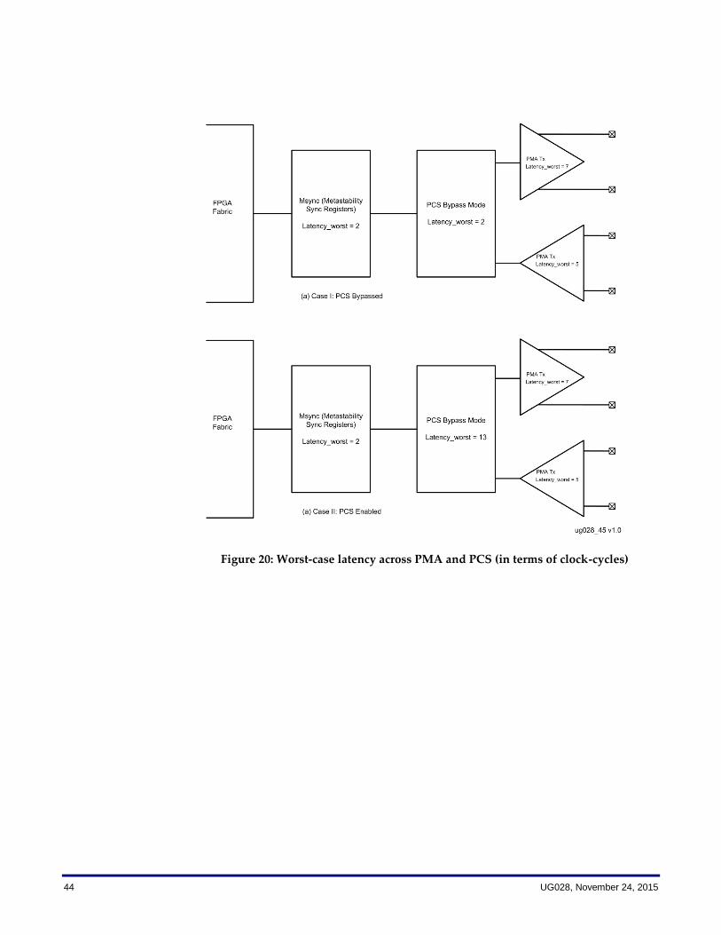
44 UG028, November 24, 2015
Figure 20: Worst-case latency across PMA and PCS (in terms of clock-cycles)
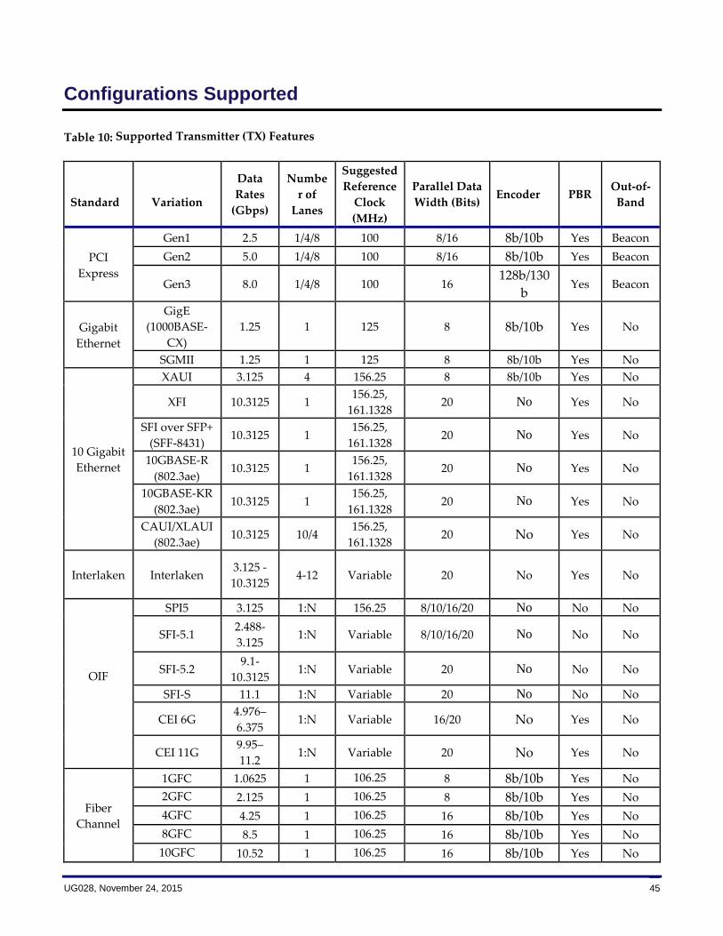
UG028, November 24, 2015 45
Configurations Supported
Table 10: Supported Transmitter (TX) Features
Standard
Variation
Data
Rates
(Gbps)
Numbe
r of
Lanes
Suggested
Reference
Clock
(MHz)
Parallel Data
Width (Bits) Encoder PBR
Out-of-
Band
PCI
Express
Gen1 2.5 1/4/8 100 8/16 8b/10b Yes Beacon
Gen2 5.0 1/4/8 100 8/16 8b/10b Yes Beacon
Gen3 8.0 1/4/8 100 16 128b/130
b Yes Beacon
Gigabit
Ethernet
GigE
(1000BASE-
CX)
1.25 1 125 8 8b/10b Yes No
SGMII 1.25 1 125 8 8b/10b Yes No
10 Gigabit
Ethernet
XAUI 3.125 4 156.25 8 8b/10b Yes No
XFI 10.3125 1 156.25,
161.1328 20 No Yes No
SFI over SFP+
(SFF-8431) 10.3125 1
156.25,
161.1328 20 No Yes No
10GBASE-R
(802.3ae) 10.3125 1
156.25,
161.1328 20 No Yes No
10GBASE-KR
(802.3ae) 10.3125 1
156.25,
161.1328 20 No Yes No
CAUI/XLAUI
(802.3ae) 10.3125 10/4
156.25,
161.1328 20 No Yes No
Interlaken Interlaken 3.125 -
10.3125 4-12 Variable 20 No Yes No
OIF
SPI5 3.125 1:N 156.25 8/10/16/20 No No No
SFI-5.1 2.488-
3.125 1:N Variable 8/10/16/20 No No No
SFI-5.2 9.1-
10.3125 1:N Variable 20 No No No
SFI-S 11.1 1:N Variable 20 No No No
CEI 6G 4.976–
6.375 1:N Variable 16/20 No Yes No
CEI 11G 9.95–
11.2 1:N Variable 20 No Yes No
Fiber
Channel
1GFC 1.0625 1 106.25 8 8b/10b Yes No
2GFC 2.125 1 106.25 8 8b/10b Yes No
4GFC 4.25 1 106.25 16 8b/10b Yes No
8GFC 8.5 1 106.25 16 8b/10b Yes No
10GFC 10.52 1 106.25 16 8b/10b Yes No

46 UG028, November 24, 2015
Standard
Variation
Data
Rates
(Gbps)
Numbe
r of
Lanes
Suggested
Reference
Clock
(MHz)
Parallel Data
Width (Bits) Encoder PBR
Out-of-
Band
SONET
OC-12 0.622 1 622.08,
155.52 8/10 No Yes No
OC-24 1.244 1 622.08,
155.52 8/10 No Yes No
OC-48 2.48832 1 622.08,
155.52 8/10 No Yes No
OC-192 9.95 1 622.08,
155.52 20 No Yes No
SATA
SATA-1 1.5 1 Variable 8/10 8b/10b No Yes
SATA-2 3.0 1 Variable 8/10/16/20 8b/10b No Yes
SATA-3 6.0 1 Variable 16/20 8b/10b No Yes
SAS
SAS-1 1.5/3.0 1 Variable 8/10/16/20 8b/10b No Yes
SAS-2 6.0 1 Variable 16/20 8b/10b No Yes
SAS-3 12.0 1 Variable 20 8b/10b No Yes
Serial
Rapid I/O
Serial Rapid
I/O – Gen1
1.25/2.5/
3.125 1 Variable 8/10/16/20 8b/10b No No
Serial Rapid
I/O – Gen2
5.0/6.12
5 1 Variable 16/20 8b/10b No No
E-PON
(802.3av)
E-PON
(802.3av)
1.25/2.5/
10 1 Variable 8/10/16/20 No No No
InfiniBand InfiniBand 2.5 / 5.0
/ 10.0 1 100 8/16 8b/10b Yes No
CPRI v5.0 614.4 –
9830.4 1 122.88 8/16 8b/10b Yes No
CPRI v6.0 10.317 1 122.88 20 No Yes No
OBSAI OBSAI 1.536 /
3.072 1 153.6 8/16 8b/10b Yes No
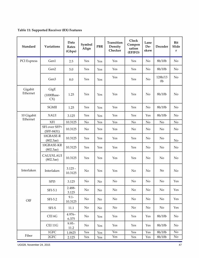
UG028, November 24, 2015 47
Table 11: Supported Receiver (RX) Features
Standard
Variations Data
Rates
(Gbps)
Symbol Align
PBR Transition
Density Checker
Clock Compen
sation (EFIFO)
Lane De-
skew Decoder
Bit Slide
r
PCI Express Gen1 2.5 Yes Yes Yes Yes No 8b/10b No
Gen2 5.0 Yes Yes Yes Yes No 8b/10b No
Gen3 8.0 Yes Yes Yes
Yes No 128b/13
0b No
Gigabit Ethernet
GigE
(1000Base-CX)
1.25 Yes Yes Yes Yes No 8b/10b No
SGMII 1.25 Yes Yes Yes Yes No 8b/10b No
10 Gigabit Ethernet
XAUI 3.125 Yes Yes Yes Yes Yes 8b/10b No
XFI 10.3125 No Yes Yes No No No No
SFI over SFP+
(SFF-8431) 10.3125 No Yes Yes No No No No
10GBASE-R
(802.3ae) 10.3125 Yes Yes Yes Yes No No
No
10GBASE-KR
(802.3ae) 10.3125 Yes Yes Yes Yes No No No
CAUI/XLAUI (802.3ae) 10.3125 Yes Yes Yes Yes No No No
Interlaken Interlaken 3.125 -
10.3125
No
Yes Yes No No No No
OIF
SPI5 3.125 No No No No No No Yes
SFI-5.1 2.488-
3.125 No No No No No No Yes
SFI-5.2 9.1-
10.3125 No No No No No No Yes
SFI-S 11.1 No No No No No No Yes
CEI 6G 4.976–
6.375 No Yes Yes Yes Yes 8b/10b No
CEI 11G 9.95–
11.2 No Yes Yes Yes Yes 8b/10b No
Fiber 1GFC 1.0625 Yes Yes Yes Yes Yes 8b/10b No
2GFC 2.125 Yes Yes Yes Yes Yes 8b/10b No
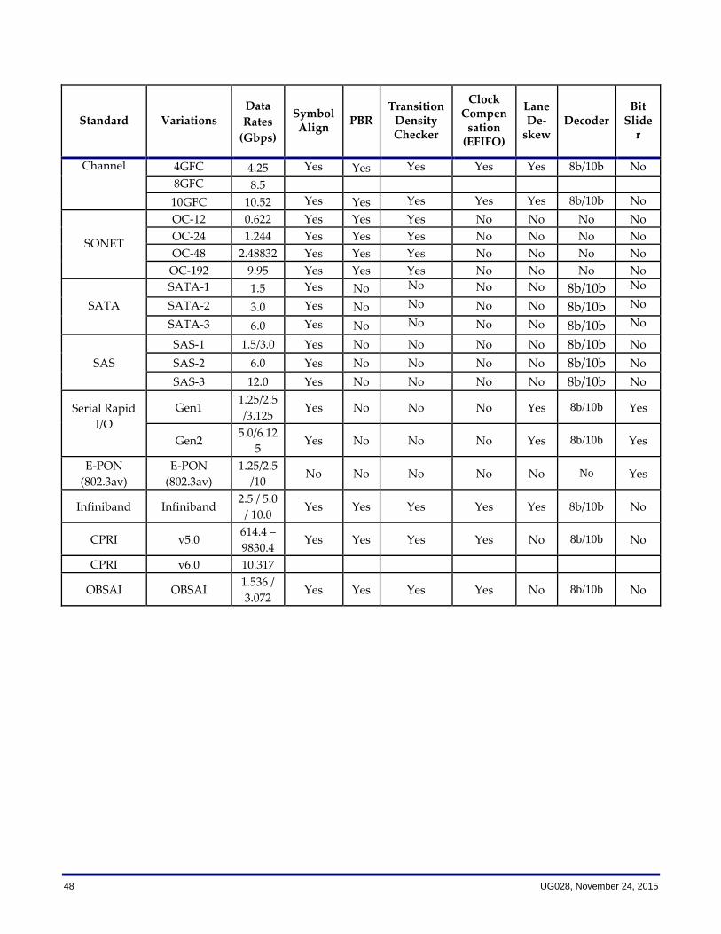
48 UG028, November 24, 2015
Standard
Variations Data
Rates
(Gbps)
Symbol Align
PBR Transition
Density Checker
Clock Compen
sation (EFIFO)
Lane De-
skew Decoder
Bit Slide
r
Channel 4GFC 4.25 Yes Yes Yes Yes Yes 8b/10b No
8GFC 8.5
10GFC 10.52 Yes Yes Yes Yes Yes 8b/10b No
SONET
OC-12 0.622 Yes Yes Yes No No No No
OC-24 1.244 Yes Yes Yes No No No No
OC-48 2.48832 Yes Yes Yes No No No No
OC-192 9.95 Yes Yes Yes No No No No
SATA
SATA-1 1.5 Yes No No No No 8b/10b No
SATA-2 3.0 Yes No No No No 8b/10b No
SATA-3 6.0 Yes No No No No 8b/10b No
SAS
SAS-1 1.5/3.0 Yes No No No No 8b/10b No
SAS-2 6.0 Yes No No No No 8b/10b No
SAS-3 12.0 Yes No No No No 8b/10b No
Serial Rapid
I/O
Gen1 1.25/2.5
/3.125 Yes No No No Yes 8b/10b Yes
Gen2 5.0/6.12
5 Yes No No No Yes 8b/10b Yes
E-PON
(802.3av)
E-PON
(802.3av)
1.25/2.5
/10 No No No No No No Yes
Infiniband Infiniband 2.5 / 5.0
/ 10.0 Yes Yes Yes Yes Yes 8b/10b No
CPRI v5.0 614.4 –
9830.4 Yes Yes Yes Yes No 8b/10b No
CPRI v6.0 10.317
OBSAI OBSAI 1.536 /
3.072 Yes Yes Yes Yes No 8b/10b No

UG028, November 24, 2015 49
Design Flow: Creating a SerDes Design
In this chapter, step-by-step instructions for creating a SerDes design are presented:
1. Generation of SerDes wrapper using ACE GUI
2. Design of top-level RTL to instantiate the SerDes wrapper created in step 1.
3. Definition of placement and timing for the SerDes.
4. Design guidelines
This chapter starts with a simple design and presents step-by-step instructions for creating this design. Later section presents the additional/reduced steps required to prepare the designs with special features.
The Achronix SerDes reference design Speedster22i_SerDes_1lane_10gbps_PCS_bypass_ RD002 is a variant of the designs presented in this chapter and contains the code base used for using Achronix SerDes IP.
The first simple design presented in this chapter is named as simple_serdes_design. This is a single-lane SerDes design with the properties listed below.
Design name : simple_serdes_design Objective : Send data from fabric to SerDes and read-back data using internal loopback. Data rate : 10.3125 Gbps Standard : Generic Number of lanes : 1 Placement : South lane# 8 Ref. clock : 156.25 Mhz Data width : 40 PCS blocks : Enabled 8b/10b encoder 8b/10b decoder Symbol alignment: Automatic mode Note: clock compensation (EFIFO) not used.
The directory structure is not a hard requirement and the user may change it. The directory structure for the baseline sample design is shown below; the reference design Speedster22i_SerDes_1lane_10gbps_PCS_bypass_RD002 uses a similar directory structure.
simple_serdes_design (root for this design) |- src |----- ace (will contain the project file for generation of wrapper as well as the ace-generated wrapper, placement and timing constraint files) |----- constraints (will contain the user-defined placement and timing constraint files) |----- tb (will contain the user-defined testbench and other related files) |----- rtl (will contain the user-defined top-level rtl for the design)
Generating SerDes Wrapper using ACE GUI
This section will focus on creating SerDes wrapper using ACE GUI. The generated files will be stored in simple_serdes_design/ace folder. ACE will generate the RTL for SerDes wrapper as well as placement and timing constraint files. The SerDes wrapper module is instantiated in top-level module; the ace-generated placement and timing constraint files are used to prepare design-specific constraint files.

50 UG028, November 24, 2015
The user is assumed to have basic understanding of using ACE GUI. The user may refer to the online demo as well as the ACE documentation for different aspects of using the ACE GUI.
Single-Lane Serdes Wrapper
To generate a SerDes wrapper from ACE, the user needs to invoke ace following the instructions detailed in the ACE documentation. SerDes wrapper is created from the IP Configuration perspective. To access this perspective, from the menu-bar of ACE GUI, the user needs to select Windows, then Open Perspective and finally IP Configuration. Alternatively, the IP configuration perspective can be opened by clicking the toolbar button, shown in Figure 21: Opening IP Configuration Perspective.
Figure 21: Opening IP Configuration Perspective
Sub-Windows: The IP configuration perspective contains the following sub-windows, the arrangement of which may depend on the last saved setting for ACE GUI:
Main Window: The middle-top window. This will contain the entry boxes that are used for defining the SerDes configurations.
IP Libraries: Displays a list of the available IP libraries.
TCL Console: Displays the console messages, including warnings and errors.
IP Problems: Displays any invalid setting that you may have used while generating the wrapper.
Outline: Outline of the IP that are being generated. Wrapper for any IP will have multiple pages for user-entries. Clicking on a topic listed in Outline window, the user can go to the corresponding page.
IP Diagram: Connection diagram for the IP block. For SerDes design, it will show the connection diagram for the SerDes.

UG028, November 24, 2015 51
To generate a SerDes wrapper, the user will need to double click on the link 12G SerDes in IP Libraries window. This will bring up the window for creating new IP (SerDes) configuration as shown in Figure 22: New IP Configuration Window.
Tip: The windows listed above can be resized and moved around like any other GUI based applications. The windows can also be docked into ACE-GUI or undocked from ACE GUI.
Figure 22: New IP Configuration Window
For the current example design, a new project simple_serdes_design.acxip is created in simple_serdes_design/src/ace folder. The user can click on the button Browse to select a destination folder and type the name of the project (.acxip file) in the File name box. Clicking on Finish on this window will create the project and the main window will be populated, as shown in Figure 23: New IP Configuration Window- Overview Page.

52 UG028, November 24, 2015
Figure 23: New IP Configuration Window- Overview Page
The user will now have the Overview page in the main window with the options for entering design parameters. The Outline and IP Diagram windows are also populated at this point, as shown in “ Figure 24: Outline Window” and “Figure 25: IP Diagran Window”.
Figure 24: Outline Window
Figure 25: IP Diagran Window
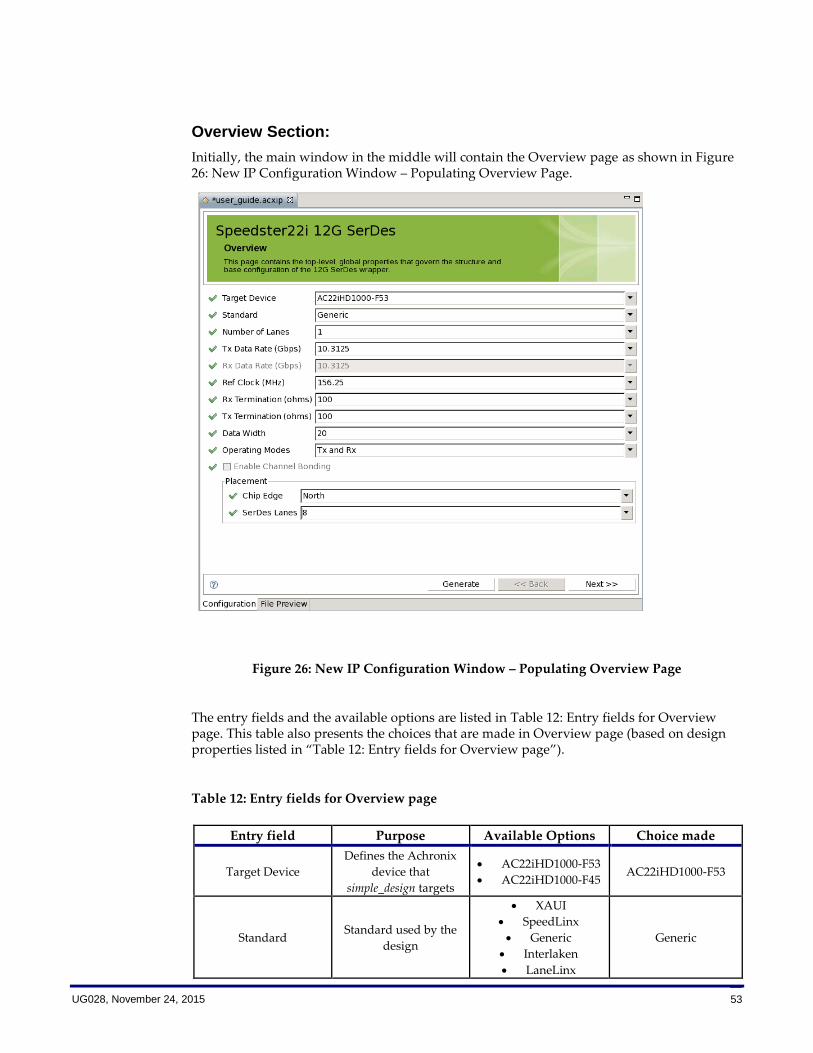
UG028, November 24, 2015 53
Overview Section:
Initially, the main window in the middle will contain the Overview page as shown in Figure 26: New IP Configuration Window – Populating Overview Page.
Figure 26: New IP Configuration Window – Populating Overview Page
The entry fields and the available options are listed in Table 12: Entry fields for Overview page. This table also presents the choices that are made in Overview page (based on design properties listed in “Table 12: Entry fields for Overview page”).
Table 12: Entry fields for Overview page
Entry field Purpose Available Options Choice made
Target Device
Defines the Achronix
device that
simple_design targets
AC22iHD1000-F53
AC22iHD1000-F45 AC22iHD1000-F53
Standard Standard used by the
design
XAUI
SpeedLinx
Generic
Interlaken
LaneLinx
Generic

54 UG028, November 24, 2015
Entry field Purpose Available Options Choice made
Number of Lanes Number of lanes used
by the design 1 to 12. 1
TX Data Rate (Gbps) TX data rate for the
design
12 options ranging
from 1.0265 to 11.31*1 10.3125
RX Data Rate (Gbps)
RX data rate for the
design is currently
disabled. ACE GUI
makes it equal to the
TX Data Rate. *1 *3
Ref. Clock (MHz) Reference clock for
SerDes PLL’s.
18 options ranging
from 60MHz to 350
MHz, including the
reference frequency for
typical protocols. *1
156.25 MHz
RX Termination Termination resistance
used for Receive Path
Disconnect
85
100
120
100
TX Termination
Termination resistance
used for Transmitter
Path
Disconnect
85
100
120
100
Data Width
Defines the number of
data bits used by the
SerDes interface
16
20
20
Operating Mode
Whether the SerDes
will be used for RX or
TX or both.
RX only
TX only
TX and RX
TX and RX
Enable Channel
Bonding
Whether the design
uses bonded lanes
True
False
The check-box is
enabled only when the
design uses multiple
lanes. The user must
use lane-bonding if
number of lanes is
more than 4.
Not applicable for
single-lane
simple_serdes_design
Placement:
Chip Edge Defines the location of
the SerDes lane used.
North
South
Implies the North and
South sides of Achronix
FPGA*2
North
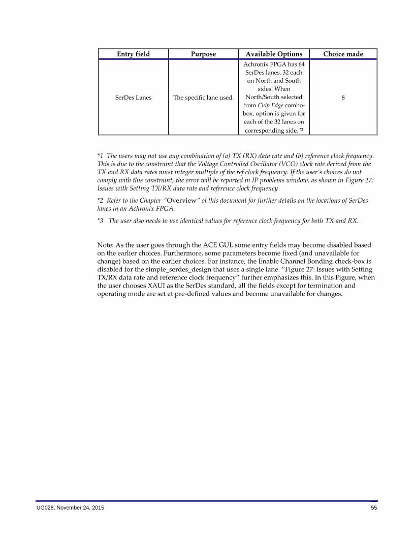
UG028, November 24, 2015 55
Entry field Purpose Available Options Choice made
SerDes Lanes The specific lane used.
Achronix FPGA has 64
SerDes lanes, 32 each
on North and South
sides. When
North/South selected
from Chip Edge combo-
box, option is given for
each of the 32 lanes on
corresponding side. *2
8
*1 The users may not use any combination of (a) TX (RX) data rate and (b) reference clock frequency. This is due to the constraint that the Voltage Controlled Oscillator (VCO) clock rate derived from the TX and RX data rates must integer multiple of the ref clock frequency. If the user’s choices do not comply with this constraint, the error will be reported in IP problems window, as shown in Figure 27: Issues with Setting TX/RX data rate and reference clock frequency
*2 Refer to the Chapter-“Overview” of this document for further details on the locations of SerDes lanes in an Achronix FPGA.
*3 The user also needs to use identical values for reference clock frequency for both TX and RX.
Note: As the user goes through the ACE GUI, some entry fields may become disabled based on the earlier choices. Furthermore, some parameters become fixed (and unavailable for change) based on the earlier choices. For instance, the Enable Channel Bonding check-box is disabled for the simple_serdes_design that uses a single lane. “Figure 27: Issues with Setting TX/RX data rate and reference clock frequency” further emphasizes this. In this Figure, when the user chooses XAUI as the SerDes standard, all the fields except for termination and operating mode are set at pre-defined values and become unavailable for changes.
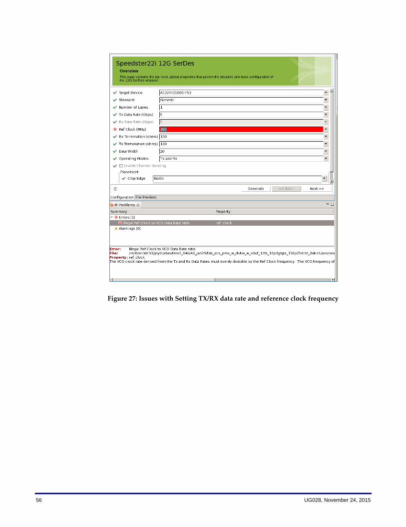
56 UG028, November 24, 2015
Figure 27: Issues with Setting TX/RX data rate and reference clock frequency

UG028, November 24, 2015 57
Figure 28: Unavailable Fields
As “Figure 28: Unavailable Fields” shows Some fields become unavailable based on earlier choices made by the user. In this case, the user chooses ‘XAUI’ as the standard (not related to simple_serdes_design)
Note: For the data-rate above 5.0 GBPS (including 10.3125 GBPS), the ACE GUI eventually uses the wide-bus architecture and generates a wrapper that transmit/receive 40-bit data from/to fabric. A later section of this chapter further details the wide-bus architecture.
Section on PMA Settings:
Clicking Next button on Overview page will bring up the section on PMA Settings. The first page for PMA Settings is shown in “Figure 29: PMA Settings Window – First page”. Alternatively, the user can click on PMA Settings on the Outline window of “ Figure 24: Outline Window”.

58 UG028, November 24, 2015
Figure 29: PMA Settings Window – First page
The first page of the PMA Settings section gives the options to enter lane-specific PMA settings. This is not relevant to the current design since it uses a single SerDes lane. However, for completion, “Figure 30: Outline Window, When Lane-Specific PMA Settings are Enabled” shows the Outline sub-window when the user enables lane-specific RX PMA Equalization and lane-specific RX PMA PLL.
For the single-lane simple_serdes_design, the PMA Settings section consists of the following four sub-sections and the corresponding list is displayed in Outline window (top-right sub-window in “Figure 30: Outline Window, When Lane-Specific PMA Settings are Enabled”):
1. RX PMA Equalization
2. RX PMA PLL
3. TX PMA Driver and
4. TX PMA PLL
The user can browse through these sub-sections by clicking Next buttons or by selecting a page from the Outline window.

UG028, November 24, 2015 59
Figure 30: Outline Window, When Lane-Specific PMA Settings are Enabled
RX PMA Equalization
This page allows the user to change the PMA equalization settings on the receive path. The entry fields and the available options are listed in “Table 13: RX PMA Equalization”. This table also presents the choices that are made for the current design: simple_serdes_design.
Note: All analog settings in “Table 13: RX PMA Equalization” and the tables to follow are provided for reference only. For challenging physical links, the equalization settings need to be tuned by the user.
Table 13: RX PMA Equalization
Entry field Purpose Available Options* Choice made
Low Freq AGC
Gain
Automatic Gain Control (AGC)
to make the SerDes suitable
over a range of signal levels
Disconnected
-18.1 dB
-12.2 dB
-8.7 dB
-6.2 dB
-4.3 dB
-2.7 dB
-1.3 dB
-18.1 dB
(default)
High Freq AGC
DC Gain
Control DC Gain of High
Frequency RX AGC
-2.94 dB
-1.3 dB
0.332 dB
1.97 dB
3.6 dB
5.21 dB
-2.94 dB
(default)
60 UG028, November 24, 2015
Entry field Purpose Available Options* Choice made
High Freq AGC
AC Boost
Control AC boost of High
frequency AGC
32 options ranging from
0.4 dB to 18.3 dB
Min 0: Boost 0.7dB
Max 31: Boost 22.6dB
7.8 db (default)
DFE Pulse-
shaping Tap 3dB
Freq
3dB Frequency of Pulse-Shaped
Analog
Decision Feedback Equalizer
used to
deal with channel loss
105 MHz
179 MHz
281 MHz
391 MHz
494 MHz
567 MHz
663 MHz
808 MHz
105 MHz
(default)
DFE Pulse-
shaping Tap
Gain
Tap gain of Pulse-Shaped
Analog
Decision Feedback Equalizer
used to
deal with channel loss
No pulse shaping tap
-0.38 dB
-0.78 dB
-1.20 dB
-1.63 dB
-2.09 dB
-2.58 dB
-3.10 dB
No pulse
shaping tap
(default)
DFE N-1 Tap
Gain Control
(mV)
Additional DFE taps to
equalize channel discontinuities
-59.99 mV to +59.99 mV at
8.57 mV interval 0 (default)
DFE N-2 Tap
Gain Control
(mV)
Additional DFE taps to
equalize channel discontinuities
-49.98 mV to +49.98 mV at
7.14 mV interval 0 (default)
DFE N-3 Tap
Gain Control
(mV)
Additional DFE taps to
equalize channel discontinuities
-39.97 mV to +39.97 mV at
5.71 mV interval 0 (default)
DFE N-4 Tap
Gain Control
(mV)
Additional DFE taps to
equalize channel discontinuities
-29.96 mV to +29.96 mV at
4.28 mV interval 0 (default)
RX User Control
From Fabric
True*1
False False (default)
*1 If True is selected, the ACE GUI will add two input ports to the wrapper RTL. This change is reflected in IP Diagram sub-window by the two additional ports: ch0_i_pma_RXeqlut[32:0] and ch0_i_pma_RXeqlut_str.
* Available options listed here are the current ones based on characterization data. These values are subject to change.
RX PMA PLL
This page allows the user to configure the PMA PLL settings on the receive path. The entry fields and the available options are listed in “Table 14: RX PMA PLL Settings”. This table also presents the choices that are made for the current design: simple_serdes_design.

UG028, November 24, 2015 61
Table 14: RX PMA PLL Settings
Entry field Purpose Available Options Choice made
RX PPM
Controls the frequency accuracy
threshold (ppm) for lock
detection in the CDR
Text-box entry. The user
may enter any value. 2000 (Default)
User-controlled
CDR switch
Whether the user wants to use a
switch for clock data recovery
True
False
False (Default)
62 UG028, November 24, 2015
TX PMA Driver
This page allows the user to configure the transmit driver settings on PMA.. The entry fields and the available options are listed in “Table 15: TX PMA Driver Settings”. This table also presents the choices that are made for the current design: simple_serdes_design.
Table 15: TX PMA Driver Settings
Entry field Purpose Available Options Choice made
Transmit Amplitude
(mVdiff-pkpk)
Transmit Amplitude control
signal. Used to define the
full-scale maximum swing of
the driver.
952
1024
1094
1163
1227
1283
1331
1331 (Default)
Cursor Level N
Defines the total number of
driver units allocated in the
driver
Text field to enter any
value 21 (Default)
Per-Cursor Level N+1
Defines the total number of
driver units allocated to the
first pre-cursor (C-1) tap.
Text field to enter any
value 0 (Default)
Post-Cursor Level N-1
Defines the total number of
driver units allocated to the
first pre-cursor (C+1) tap.
Text field to enter any
value 4 (Default)
Post-Cursor Level N-2
Defines the total number of
driver units allocated to the
second post-cursor (C+2) tap.
Text field to enter any
value 0 (Default)
Slew Rate TX driver Slew Rate control
31 ps
33 ps
68 ps
170 ps
31 ps (Default)
TX User Control from
Fabric
True
False False (Default)
This page also lists additional TX PMA driver related information (to facilitate user-choices):
• Maximum Bit Amplitude (mVpp): 1173
• Back-Porch Bit Amplitude (mVpp): 861
• Preshoot Level (dB): 0.00
• De-emphasis Level (dB): -2.69
TX PMA PLL
This page allows the user to configure the PMA PLL settings on the transmit path. There is one entry field in this page for simple_serdes_design, as listed in “Table 16: TX PMA PLL Settings”:
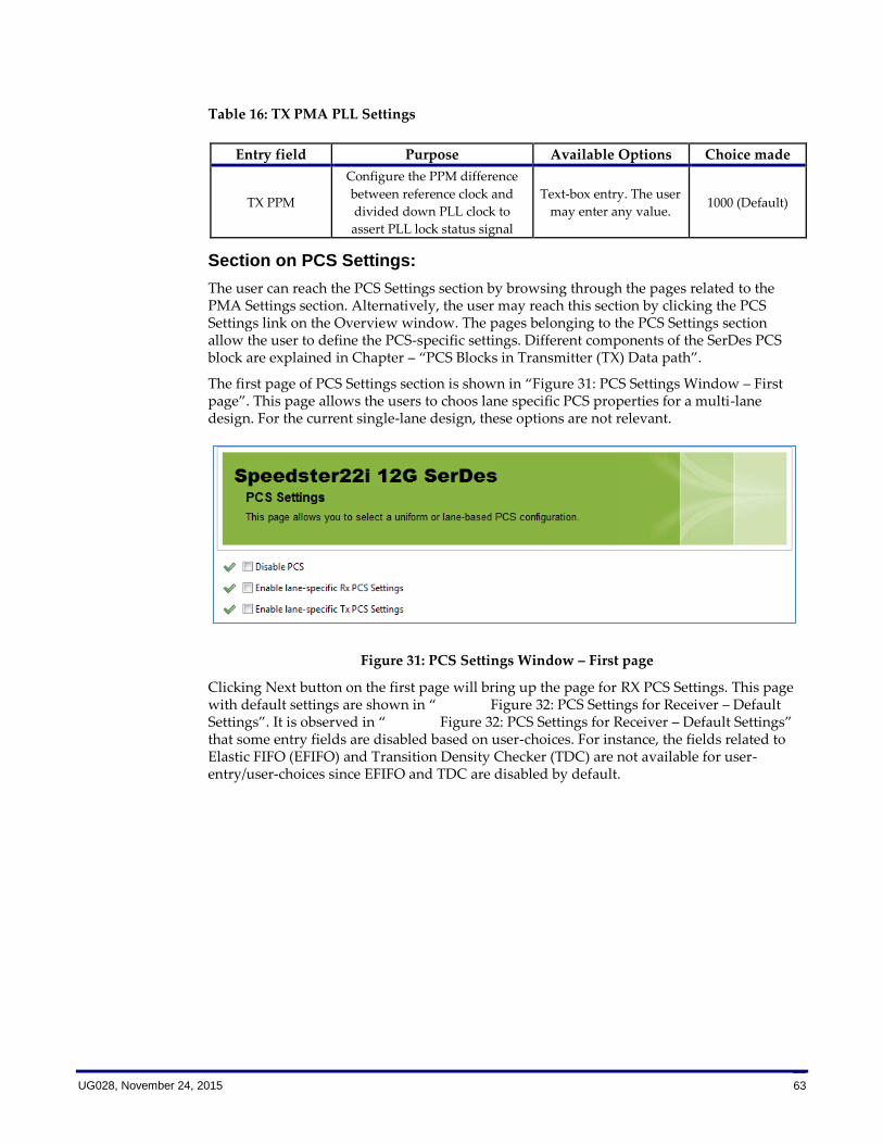
UG028, November 24, 2015 63
Table 16: TX PMA PLL Settings
Entry field Purpose Available Options Choice made
TX PPM
Configure the PPM difference
between reference clock and
divided down PLL clock to
assert PLL lock status signal
Text-box entry. The user
may enter any value. 1000 (Default)
Section on PCS Settings:
The user can reach the PCS Settings section by browsing through the pages related to the PMA Settings section. Alternatively, the user may reach this section by clicking the PCS Settings link on the Overview window. The pages belonging to the PCS Settings section allow the user to define the PCS-specific settings. Different components of the SerDes PCS block are explained in Chapter – “PCS Blocks in Transmitter (TX) Data path”.
The first page of PCS Settings section is shown in “Figure 31: PCS Settings Window – First page”. This page allows the users to choos lane specific PCS properties for a multi-lane design. For the current single-lane design, these options are not relevant.
Figure 31: PCS Settings Window – First page
Clicking Next button on the first page will bring up the page for RX PCS Settings. This page with default settings are shown in “ Figure 32: PCS Settings for Receiver – Default Settings”. It is observed in “ Figure 32: PCS Settings for Receiver – Default Settings” that some entry fields are disabled based on user-choices. For instance, the fields related to Elastic FIFO (EFIFO) and Transition Density Checker (TDC) are not available for user-entry/user-choices since EFIFO and TDC are disabled by default.

64 UG028, November 24, 2015
Figure 32: PCS Settings for Receiver – Default Settings
RX PCS Settings
This page allows the user to configure the RX PCS settings. The entry fields and the available options are listed in “Table 17: RX PCS Settings”. This table also presents the choices that are made for the current design: simple_serdes_design.
Table 17: RX PCS Settings
Entry field Purpose Available Options Choice made
Decoder*3
Decoder to be used by
the design on the
receive side
Disabled
8b/10b
128/130b
8B10B (8b/10b)
decoder
Polarity Bit Reversal (PBR) Functions
PBR Block*3
If the user chooses to
use PBR. It should
match with the PBR
technique used on TX-
side. On TX-side, PBR0
is used on pre-encoded
data and PBR1 is used
on post-encoded data
to PMA.
PBR0
PBR1 PBR0 (Default)
Receive Symbol Swap*3 Related to PBR block. True
False False
Receive Bit Order
Reverse*3 Related to PBR block.
True
False False
Receive Polarity
Reverse*3 Related to PBR block.
True
False False

UG028, November 24, 2015 65
Entry field Purpose Available Options Choice made
Elastic FIFO*3
Use Elastic FIFO*3
Whether clock
compensation block on
PCS (i.e., EFIFO) will
be used.
True *2
False False (Default)
8B Mode*3 Whether 8B mode will
be used
True
False
N/A since EFIFO is
disabled
SKIP Mode*3 Skip mode used for
EFIFO
Disabled
802.3ae (one word)
802.3 (two words)
PCIe
N/A since EFIFO is
disabled
SKIP Word 0*3 Skip Word used for
EFIFO
Text field to select
user-defined value
N/A since EFIFO is
disabled
Eanble ALT 0*3 Whether Alternate
word will be used
True
False
N/A since EFIFO is
disabled
ALT SKIP Word 0*3 Alternate SKIP Word
used for EFIFO
Text field to select
user-defined value
(available only when
Enable ALT 1 is selected
N/A since EFIFO is
disabled
SKIP Word 1*3
Similar to the
parameters related to
Skip Word 0. *3
Text field to select
user-defined value
N/A since EFIFO is
disabled
Eanble ALT 1*3 True
False
N/A since EFIFO is
disabled
ALT SKIP Word 1*3
Text field to select
user-defined value
(available only when
Enable ALT 0 is selected
N/A since EFIFO is
disabled
SKIP Word 2*3 Text field to select
user-defined value
N/A since EFIFO is
disabled
Eanble ALT 2*3 True
False
N/A since EFIFO is
disabled
ALT SKIP Word 2*3
Text field to select
user-defined value
(available only when
Enable ALT 2 is selected
N/A since EFIFO is
disabled
Transition Density Checker (TDC)
Enable Transition
Density Checker*3
Whether TDC will be
used
True *1
False False
Max Count*3 The threshold value for
TDC
Text field for user-
defined value
(available only when
TDC is enabled)
N/A (TDC not
enabled)
Max Count Scaling
Factor*3
The maximum scaling
factor.
x1
x2
x4
x8
x16
N/A (TDC not
enabled)
*3 Further description on these parameters can be found in Section”PCS Blocks in the Receiver (RX)”

66 UG028, November 24, 2015
RX PCS Symbol Alignment
“ Figure 33: PCS Settings for Receiver – Symbol Alignment” presents the RX PCS Symbol Alignment window with the choices pertaining to the current design: simple_serdes_design.
Figure 33: PCS Settings for Receiver – Symbol Alignment
The entry fields and the available options are listed in “Table 18: Symbol Alignment Settings (PCS)”. This table also presents the choices that are made for the current design: simple_serdes_design.
Table 18: Symbol Alignment Settings (PCS)
Entry field Purpose Available Options Choice made
Symbol Alignment
Mode*1 Mode used
Disabled
Automatic
Manual
Bit Slip
Automatic
Automatic Symbol
Alignment
Align on Even Symbol
Whether alignment
operation will be on
even symbols only.
True
False False
Enable Double-Word
Alignment Mode
Whether double word
alignment will be used
True
False False
Enable Word 0 Symbol alignment
word# 0 enabled
True
False True

UG028, November 24, 2015 67
Entry field Purpose Available Options Choice made
Word 0 Value of Word# 0,
when enabled.
Text field to enter user-
defined value
(available when Word
0 is enabled)
283* (Refer to)
Mask 0 Value of mask for
word0
Text field to enter user-
defined value
(available when Word
0 is enabled)
000
Enable Word 0 or
Inverse of Word 0
Whether word 0 or the
inverse of it will be
used
True
False False
Enable Seq 0 Whether Seq0 will be
used.
True
False False
Seq 0 Value of Seq 0
Text field to enter user-
defined value
(available when Seq 0
is enabled)
N/A since Seq0 is not
enabled
Gap Count Gap Count for Seq0
Text field to enter user-
defined value
(available when Word
0 is enabled)
N/A since Seq 0 is not
enabled
Enable Alt Seq 0 Whether Alternate of
Seq0 will be used
True
False False
Alt Seq 0 Value of Alternate of
Seq 0
Text field to enter user-
defined value
(available when Alt
Seq 0 is enabled)
N/A since Alt Seq 0 is
not enabled
Enable Word 1
Similar to Word 0, Seq
0 etc.
True
False False
Word 1
Text field to enter user-
defined value
(available when Word
0 is enabled)
N/A since Word 1
Mask 1
Text field to enter user-
defined value
(available when Word
0 is enabled)
000
Enable Word 1 or
Inverse of Word 1
True
False False
Enable Seq 1 True
False False
Seq 1
Text field to enter user-
defined value
(available when Seq 0
is enabled)
N/A since Seq0 is not
enabled
Gap Count
Text field to enter user-
defined value
(available when Word
0 is enabled)
N/A since Seq 0 is not
enabled
Enable Alt Seq 1 True
False False

68 UG028, November 24, 2015
Entry field Purpose Available Options Choice made
Alt Seq 1
Text field to enter user-
defined value
(available when Alt
Seq 0 is enabled)
N/A since Alt Seq 0 is
not enabled
Unlock Mode When the unlock will
be reported
Misaligned
Decode Error
Decode or
Disparity
Misaligned
Unlock Count
The number of unlocks
before misalignment
reported
Text field to enter user-
defined value 3
Lock Count
The number of locks
before alignment is
reported
Text field to enter user-
defined value 3
Unlock Decrement
Count
Decrement count for
unlock
Text field to enter user-
defined value 1
*1 Based on user-selection, relevant ports are added to the GUI wrapper, which is reflected on the IP Diagram sub-window.
The other available symbol alignment options are Manual and Bit Slip, as detailed in Section – “Symbol Alignment”.
TX PCS Settings
“Figure 34: PCS Settings for Receiver – TX PCS Settings” presents the RX PCS Symbol Alignment window with the choices pertaining to the current design: simple_serdes_design.
Figure 34: PCS Settings for Receiver – TX PCS Settings
The entry fields and the available options are listed in “Table 19: TX PCS Settings”. This table also presents the choices that are made for the current design: simple_serdes_design.
UG028, November 24, 2015 69
Table 19: TX PCS Settings
Entry field Purpose Available Options Choice made
Encoder
Disabled
8b/ 10b
128/130b
8B10B
PBR Functions
PBR Block
Whether PBR block is
used. PBR0 is used on
data before encoder (or
when encoder is
disabled). PBR1 is used
on encoded data to
PMA.
PBR0
PBR1 PBR0
Transmit Symbol Swap Setting for PBR block
on TX path.
True
False False
Transmit Bit Order
Reverse
Setting for PBR block
on TX path.
True
False False
User-Controlled
Disparity and Error
Forcing
Option to force
disparity and error
forcing (from fabric?)
True
False False
Clicking Next on the window titled “TX PCS Settings” will bring the windows for BIST test settings. We will ignore those windows for this design.
Section on Manually Overriding PMA/PCS Register Values:
Based on the user choices made in the earlier sections, ACE has assigned the values for PMA and PCS registers at this point. The advanced user however may want to change the pre-defined value for one or more registers. This section of ACE GUI provides this option for advanced users.
Please refer to the Section - Bypassing PCS by Manually Overriding Corresponding Register for further details on this.

70 UG028, November 24, 2015
Generation of Wrapper Files:
The user can now generate wrapper files (src/ace folder) by clicking the Generate button.
Note: The user can generate the wrapper files without going through all the pages. In other words, the user can use Generate button from any page to generate the wrapper files. If the user does not set values for one or more multiple pages, ACE will use the default values for the corresponding configurations.
When the user clicks the Generate button, a pop-up window, as shown in “Figure 35: Generating the Wrapper Files” will be displayed.
Figure 35: Generating the Wrapper Files
The wrapper file locations and the names are based on the directory structure that have been used to create this design.
The option Register Dump File is disabled here. If the option is chosen with the file name, the corresponding file will provide the values of the PMA/PCS registers, based on the choices made by the user while generating the wrapper.
The option VHDL Model can be used to generate a wrapper in VHDL. The resulting VHDL file is essentially a wrapper that instantiates the Verilog model for the SerDes wrapper.

UG028, November 24, 2015 71
If the files are successfully generated, the user will find the corresponding message on the TCL sub-window, as shown in “Figure 36: TCL console message upon successful generation of wrapper files”.
Figure 36: TCL console message upon successful generation of wrapper files
Files Generated by ACE-GUI
Based on the directory structure and the file names that have been chosen (“Figure 35: Generating the Wrapper Files”), there will be up to five files in simple_serdes_design/src/ace folder:
• simple_serdes_design_wrapper.v: This file contains the RTL generated by ACE GUI. The top level module for this wrapper is simple_serdes_design_wrapper. This module will be instantiated in top level design module: simple_serdes_design.v file.
• simple_serdes_design_wrapper.vhd: If the VHDL file generation has been chosen.
• simple_serdes_design_wrapper.sdc: This file will provide the timing constraints for the SerDes PLL clocks. This file further identifies the related and unrelated clocks.
• simple_serdes_design_wrapper.pdc: This file will provide the placement of the SerDes lanes, based on the lane-positioning chosen in the Overview page (“Figure 26: New IP Configuration Window – Populating Overview Page”).
• simple_serdes_design_registers.txt: This file will provide the values for all PCS and PMA registers, based on the choices made in ACE GUI.

72 UG028, November 24, 2015
Integration of SerDes Wrapper in a Design
This section details how to use the files generated by ACE GUI into a user-design. For ready-reference, the design properties from “Design Flow: Creating a SerDes Design” are presented again:
Design name : simple_serdes_design Objective : Send data from fabric to SerDes and read-back data using internal loopback. Data rate : 10.3125 Gbps Standard : Generic Number of lanes : 1 Placement : South lane# 8 Ref. clock : 156.25 Mhz Data width : 40 PCS blocks used : 8b/10b encoder 8b/10b decoder Symbol alignment: Automatic mode Note: clock compensation (EFIFO) not used.
The simple_serdes_design will contain the following files:
simple_serdes_design_top.v: Top-level RTL that will instantiate the SerDes wrapper generated by ACE. As per the directory structure as shown above, this file will be under src/rtl sub-directory.
simple_user_design_wrapper.v: The SerDes wrapper RTL that has been generated by ACE. (Under src/ace directory.)
data_generation.v: This will include the code used to generate data for transmission, including comma characters. (Under src/rtl sub-directory.)
simple_user_design.pdc: ACE Placement file. (Under src/constraints sub-directory.)
simple_user_design.sdc: ACE constraint file for timing. This will contain the timing constraints from the ACE-generated simple_serdes_design_wrapper.sdc file as well as constraints related to the additional clocks used in simple_user_design_top.v. (Under src/constraints sub-directory.)
tb_user_guide.v: This is the testbench used for design; we will use this for simulation purposes. (Under src/tb sub-directory.)
The Achronix SerDes reference design Speedster22i_SerDes_1lane_10gbps_PCS_bypass_ RD002 can be referred for further understanding on how the ACE GUI generated files can be used in a design.
Design and Wrapper Files
simple_serdes_design_top.v: This is the top-level module for the current design. This module will instantiate the SerDes wrapper (from simple_design_wrapper.v file) and will use the SerDes ports to: (a) send data to SerDes and (b) read-back data from SerDes. Some SerDes ports are also brought to the FPGA I/O pads as reset and debug signals.
The ports that are available from the SerDes wrapper are displayed in “Figure 25: IP Diagran Window”. To instantiate the wrapper module simple_serdes_design_wrapper, the following construct is used:
simple_serdes_design_wrapper iSerDes
where, iSerDes is the name of the instance. The instance name iSerDes is used in other files as well, such as the ace_placement.pdc and the ace_constraint.sdc files. If the instance name
UG028, November 24, 2015 73
iSerDes is chosen as the Hierarchical Instance Path, the generated .sdc and .pdc files need not be modified.
“Table 20: Signals passed between the SerDes Instance and the Top-Level module” gives a list of the ports in the SerDes wrapper that are accessed from the top-level module of the current design. The corresponding signal names used in the top-level module are also listed in this Table.
Table 20: Signals passed between the SerDes Instance and the Top-Level module
SerDes Port Name Top-level Signal-name Comments
ch0_i_ba_RX_m ln0_RX_m
These input signals to SerDes
are also inputs to the top-level
RTL. Note: These signals are
connected directly from SerDes
to the package balls without
any logic in between. In other
words, the users don’t need to
insert any I/O pads.
ch0_i_ba_RX_p ln0_RX_p
ch0_i_bck_ref_m ln0_refclk_m
ch0_i_bck_ref_p ln0_refclk_p
ch0_i_RX_rst_n1 ln0_rst_n_RX
Reset inputs to the SerDes from
user logic.
Note: Same input can be used
for RX and TX reset signals.
These signals should preferably
be delayed from the hard-reset
signal. Hard reset goes to the
PMA and RX and TX resets go
to the PCS.
ch0_i_TX_rst_n1 ln0_rst_n_TX
ch0_i_rst_hard_n1 ln0_rst_hard
ch0_i_TX_datain ln0_TX_data
Transmit data input to SerDes
from user logic. (Refer to
data_generation.v presented
later.)
ch0_o_RX_data_clk ln0_RX_clk
Output from SerDes to user
logic. RX-clock generated from
SerDes and used for RX-path in
top-level, such as the checker
for the received data.
ch0_o_TX_data_clk ln0_TX_clk
Output from SerDes to user
logic. TX-clock generated from
SerDes and used for TX-path in
top-level, such as generator for
the transmitted data.
ch0_o_RX_dataoutA ln0_RX_data Receive side RX data output
from SerDes to the user logic.
ch0_o_pma_RX_cdr_lck2dat ln0_pma_RX_cdr_lck2dat
Outputs from SerDes.
These are status signals from
SerDes. These signals indicate
74 UG028, November 24, 2015
SerDes Port Name Top-level Signal-name Comments
whether the SerDes is ready.
For instance, ln0_TX_ready
indicates that the SerDes is
ready for data receipt.
These signals can be used for
debugging and other purposes.
For instance, ln0_TX_ready can
be used to start data
transmission.
ch0_o_pma_TXready ln0_pma_TXready
ch0_o_pma_synthready ln0_pma_synthready
ch0_o_pma_RXready ln0_pma_RXready
ch0_o_pma_RXstat ln0_pma_RXstat
ch0_o_pma_sig_detect ln0_pma_sig_detect
ch0_o_pma_synthstat ln0_pma_synthstat
ch0_o_pma_TXstat ln0_pma_TXstat
ch0_i_pipe_pd 2’b0
ch0_i_RX_iddq_n1 ln0_i_RX_iddq_n
Power on reset signals for PMA.
Signals can be sent to assert
these inputs certain time after
the SerDes is powered up.
ch0_i_synth_iddq_n1 Ln0_i_synth_iddq_n
ch0_i_TX_iddq_n Ln0_i_TX_iddq_n
ch0_o_RX_syma_locked ln0_RX_syma_locked
Output from SerDes to user
logic. Indicates symbol
alignment, when the module is
used.
ch0_i_sbus_clk i_sclk
Input clock-signal to the SerDes
for use with the Serial Bus
(SBUS). In this design, it is
coming from a top-level IO
clock pad. The external SBUS
clock must be running when
you program this design into
the device since the SBUS is
access in the startup sequence
to enable loopback.
ch0_i_sbus_data[1:0] ln0_sbus_wrdata sbus-related signals.
ch0_i_sbus_req ln0_sbus_req
ch0_i_sbus_sw_rst ln0_sbus_sw_rst
ch0_o_sbus_ack ln0_sbus_ack
ch0_o_sbus_data[1:0] ln0_sbus_rddata
1 These signals are part of the reset sequence and are further detailed in the section: Error! eference source not found..
Based on the table above, the user can now instantiate the SerDes module into top-level RTL.

UG028, November 24, 2015 75
Dynamically Changing the SerDes Register Values
Typically the PMA/PCS registers need not be changed during runtime. However, simple_serdes_design uses internal SerDes loopback. Internal loopback may be the starting point for the users to verify the functionality of any user-design. To enable the internal loopback, the user needs to dynamically ( at run-time) set a PCS register via the SBUS interface. This is done using the ACX_SERDES_LOOPBACK_CTRL module explained in Chapter – “Dynamic Read/Write of SerDes Registers via SBUS”. Internal loopback cannot be programmed statically (in the ACE-generated bitstream). Section Loopback Modes presents the loopback modes available with Achronix SerDes. The code below shows an example of using ACX_SERDES_LOOPBACK_CTRL (reproduced from Chapter – “Dynamic Read/Write of SerDes Registers via SBUS” for ready reference).
Using sBus module to enable internal loopback
The code below shows how to enable internal loopback using the sBus
wire sbus_ln0_done; wire inv_sbus_disable_loopback_ln0; assign inv_sbus_disable_loopback_ln0 = ~i_sbus_disable_loopback; wire unused_ln0_i_reg_write; wire unused_ln0_i_reg_rw_req; wire unused_ln0_i_reg_pma; wire unused_ln0_i_reg_address; wire unused_ln0_i_reg_wr_data; wire unused_ln0_o_reg_rd_data; wire unused_ln0_o_reg_rdwr_valid; ACX_SERDES_LOOPBACK_CTRL #( .LOOPBACK_MODE (`LPBK_TX_RX_PMA_INTERNAL), .ENABLE_PASS_THROUGH(0) ) i_loopback_ctl_ln0 ( .sbus_clk (i_sclk), .rstn (1'b1), // ok to tie high .disable_loopback (inv_sbus_disable_loopback_ln6), // rising edge disables loopback .done (sbus_ln0_done), // program is finished // serdes connections .from_sbus_data (ln0_sbus_rddata[1:0]), .from_sbus_ack (ln0_sbus_ack), .to_sbus_data (ln0_sbus_wrdata[1:0]), .to_sbus_req (ln0_sbus_req), .i_pma_synthready (ln0_synthready), .i_pma_TXready (ln0_TX_ready), .i_pma_RXready (ln0_RX_ready), .to_sbus_sw_rst (ln0_sbus_sw_rst), // pass-through connections, can be used when 'done' is high // (ignored if ENABLE_PASS_THROUGH = 0) .i_reg_write (unused_ln0_i_reg_write), // request is ‘write' .i_reg_rw_req (unused_ln0_i_reg_rw_req), // rising edge starts action .i_reg_pma (unused_ln0_i_reg_pma), // address is pma address .i_reg_address (unused_ln0_i_reg_address), // 16-bit pcs or pma address
76 UG028, November 24, 2015
.i_reg_wr_data (unused_ln0_i_reg_wr_data), // data for write .o_reg_rd_data (unused_ln0_o_reg_rd_data), // data from read (latch when o_reg_rdwr_valid) .o_reg_rdwr_valid (unused_ln0_o_reg_rdwr_valid) // action finished (high for one cycle) );
Note: Not all registers can be modified dynamically. For a list of the dynamic registers, please contact Achronix Customer Support.
Note: To use external loopback (cables), the ACX_SERDES_LOOPBACK_CTRL instance needs to be removed from the design logic, or simply change the LOOPBACK_MODE parameter to disable internal loopback.
simple_serdes_design_wrapper.v: This is the wrapper file generated by ACE GUI. No change is required in this file for the current design.
data_generation.v: This file generates TX data for SerDes. The data generated are 40-bits. Comma characters are also generated in this file. The port-definitions for the module data_generation is shown below.
module data_generation ( input clk, input rst_n, input data_gen_en, output [39:0] data_out );
This module requires clock signal, reset signal and enable signal as inputs. For TX data, the transmit-side clock-signal and the transmit-side reset-signal are used as inputs. In the current design, the data generation is enabled only when PMA is ready for it’s operation. User may use any one or more of the following signals to enable the data-generation. However, we prefer using TXready or synthready as enable signal to decouple the TX path from the RX path:
ln0_pma_RXready,
ln0_pma_TXready,
ln0_pma_synthready and
In0_pma_RX_cdr_lck2dat
The instantiation of data_generation in the top-level module is shown in the code below.
data_generation idata_generation ( .clk (ln0_TXclk), // TX-clock from SerDes .rst_n (ln0_rst_n_TX), // TX-reset used for SerDes .data_gen_en (ln0_pma_TXready), // TX-ready signal from SerDes .data_out (ln0_TX_data) // TX-data to SerDes );
Data generated by the data_generation module needs to include comma characters. For simple_serdes_design, 10’h1BC is used as comma character. This complies with the values 10’h283 and 10’h17C that has been set as symbol alignment characters earlier in the ACE GUI. The user may refer to section “Symbols and Comma Character” for details on these characters.

UG028, November 24, 2015 77
Note: When 10’h1BC is transmitted from the fabric, the output of the 8b/10b decoder on the PCS receiver path will be 10’h283 (alternate: 10’h17C).
The code for data_generation module that includes comma-characters is shown below
module data_generation ( input clk, input rst_n, input data_gen_en, output [39:0] data_out );
always @ (posedge clk) begin if (rst_n == 1'b0) // comma-characters when SerDes in reset-state (active-low reset) data_out <= {10'h000,10'h1BC,10'h000,10'h1BC}; else if (data_gen_en == 1’b1) // when data-generation enabled, i.e. TX_ready from SerDes is up // *** Logic for data-generation goes here, such as PRBS-7 *** // *** Should also contain comma characters *** else // comma-characters when data generation is ‘not’ enabled ln0_TXdata <= {10'h000,10'h1BC,10'h000,10'h1BC}; end endmodule
Using the clocks from SerDes: This sample design has the EFIFO disabled. Hence, two clocks are provided by the SerDes for the fabric: TX-clock and RX-clock. These two clocks may not be aligned with each other. To avoid the false paths, the user needs to use the TX-clk on the transmitter datapath (such as data generation for SerDes) and the RX-clk on the receive data path (such as checking the received data from SerDes for correctness).
Placement of SerDes
The placement file used for the simple_serdes_design is: src/constraints/ace_placement.pdc. This file contains the placement information for the followings:
• Placement information for the SerDes instance
• Clock/reset inputs to the SerDes
• Debug signals that the user may want to bring outside the FPGA.
The placement of SerDes depends on the lane that the user wants to use. While generating the wrapper from ACE GUI, lane# 8 has been chosen for placement (“Figure 23: New IP Configuration Window- Overview Page”). The consequent placement in simple_serdes_design_wrapper.pdc file will be:s
set_placement -batch -fixed { i:x_ch0.u_serdes_wrap.u_serdes } { s:te_serdes_12lane_top_i1.u_serdes_lane_top_wrap_i0.u_serdes_lane_top }
Since, the SerDes instance as iSerDes in the top-level module, the placement needs to be modified as:
set_placement -batch -fixed { i:iSerDes.x_ch0.u_serdes_wrap.u_serdes } { s:te_serdes_12lane_top_i1.u_serdes_lane_top_wrap_i0.u_serdes_lane_top }
For information about how to place the clock signals, reset signals (such as rst_hard in the listing above) and other debug signals (such as ln0_synthready), please refer to the UG001 – ACE Users Guide. For the Speedster22i HD1000 Development Kit, the following three show
78 UG028, November 24, 2015
the placement of SerDes-Reset signal (ln0_rst_hard); TX-ready status signal (ln0_TX_ready) and the placement of the sbus-clock that is required to set internal-loopback through sbus interface
# Manually entered Design-specific: For providing sbus-clock for sbus-interface # The pin (pad0_clk_bank_se) refers to the clock-supply used in Achronix Validation Board. set_placement -fixed -batch {p:i_sclk} {d:pad0_clk_bank_se} #SerDes reset set_placement -batch -fixed {p:ln0_rst_hard} { d:pad0_clk_bank_nw } # TX_ready signal is brought to a LED (active-low) set_placement -batch -fixed {p:ln0_pma_TXready} { d:pad_ws_byteio9_dq3 }
Timing Constraints
Using the directory structure defined earlier, the timing constraints will be in the file
src/constraints/ace_constraint.sdc. The ACE GUI generates template for timing constraints
used for the respective SerDes design. For instance, for simple_serdes_design, timing
constraint has been generated as src/ace/simple_serdes_design_wrapper.sdc file (“
Figure 35: Generating the Wrapper Files”). This ACE-generated file can be used as a template for defining the timing constraints of a SerDes design. However, the user must manually enter the design related constraints, which are not generated by ACE for obvious reasons.
The simple_serdes_design that is being described here requires such clocks that the user needs to provide. In the following code-snippet, the SerDes reference clocks from “Table 20: Signals passed between the SerDes Instance and the Top-Level module” as well as snapshot clocks have been added to the ACE-generated constraints. (Please refer to the ACE User Document for further details on using snapshot debugging tool into a design.)
#Reference clocks # Manually entered Design-specific: For providing 156.25 reference clocks to SerDes create_clock -period 6.4 refclkp create_clock -period 6.4 refclkn # Manually entered Design-specific: For providing 50MHz clock to sbus-clock. create_clock -period 20 i_sclk # Manually entered Design – specific: SNAPSHOT clocks # Clock for snapshot and for jtap create_clock -period 100 tck # Uset-entered set_clock_groups –asynchronous –group {tck } # From ACE – generated constraint file: # Lane RX Clocks # Period (ns) = 1/(RX data rate / RX 8b10b-encoded data width) # 1.9393939393939394 = 1/(10.3125 / 20.0) # Unrelated Clock Mode: All lane-to-lane clocks are unrelated EXCEPT between the TX clocks - Elastic buffer is disabled create_clock -period 1.93939393939394 iSERDES.x_ch0.u_serdes_wrap.u_serdes/o_RX_data_clk create_clock -period 1.93939393939394 iSERDES.x_ch0.u_serdes_wrap.u_serdes/o_TX_data_clk # Lane Clock Divider Generated Clocks

UG028, November 24, 2015 79
# Unrelated Clock Mode: All lane-to-lane clocks are unrelated - Elastic buffer is disabled create_generated_clock iSERDES.x_ch0.iffdmux.GEN_CLKDIV.TX.iTXclkdiv/clk_out –source iSERDES.x_ch0.u_serdes_wrap.u_serdes/o_TX_data_clk -divide_by 2 create_generated_clock iSERDES.x_ch0.iffdmux.GEN_CLKDIV.RX.RX.iRXclkdiv/clk_out -source iSERDES.x_ch0.u_serdes_wrap.u_serdes/o_RX_data_clk -divide_by 2 # Complete: ACE - generated constraints # Clock-grouping : For Both ACE-generated and design-specific clocks # The user may refer to the ACE documentation for further details on clock-grouping (???) # Grouping all clocks: helps decision making during the place-and-route set_clock_groups -asynchronous -group {iSERDES.x_ch0.u_serdes_wrap.u_serdes/o_RX_data_clk}\ -group {iSERDES.x_ch0.u_serdes_wrap.u_serdes/o_TX_data_clk} \ -group {iSERDES.x_ch0.iffdmux.GEN_CLKDIV.TX.iTXclkdiv/clk_out} \ -group {iSERDES.x_ch0.iffdmux.GEN_CLKDIV.TX.iRXclkdiv/clk_out} \ -group {tck core_tck} -group {i_sclk}
Test bench Setup for Simulation
Based on the primary inputs and primary outputs listed in “Table 20: Signals passed between the SerDes Instance and the Top-Level module”, testbench may now be created as shown below:
module tb_fab_pcs_pma_no_ebuf_1ln_10p3125gbps_156p25mhz(); reg ch0_ref_clk_p; reg ch0_reset_signal; reg ch0_RX_output; initial begin ch0_ref_clk_p = 1'b0 ; ch0_reset_signal = 1'b0 ; #4000; ch0_reset_signal = 1'b1 ; end // Generating 156.25 MHz reference clock always #3200 ch0_ref_clk_p = ~ch0_ref_clk_p; fab_pcs_pma_no_ebuf_1ln_10p3125gbps_156p25mhz DUT( // Okay to tied to 1'b1 .ln0_RX_m (1'b1), .ln0_RX_p (1'b1), // 156.25 MHz differential reference clocks .ln0_refclk_m (~ch0_ref_clk_p), .ln0_refclk_p (ch0_ref_clk_p), // Same reset input for hard-reset, RX-reset & TX-reset .ln0_rst_n_RX (ch0_rst_hard_n), .ln0_rst_n_TX (ch0_rst_hard_n), .ln0_rst_hard (ch0_rst_hard_n), .ln0_RX_data (ch0_RX_output) ); Endmodule

80 UG028, November 24, 2015
Design Guidelines
This section will first present the coding practice that the user is recommended to use.
Reset Sequence
The following sequence is presented as a guidance to define the reset signals (Table 20:
Signals passed between the SerDes Instance and the Top-Level module”) to be used with a
typical SerDes application. The minimum timing requirements are with reference to the
keep-alive clock which runs at 27 MHz (for non wide bus interface) and at 13.7 MHz (for
wide bus interface)
1. De-assert hard-reset (ch0_i_rst_hard_n ) after at least 600µs .
2. After hard reset de-assertion, wait for at least 600µs and then de-assert the iddq reset
signals( ch0_i_tx_iddq_n, ch0_i_rx_iddq_n and ch0_i_synth_iddq_n)
3. After iddq signals are de-asserted, wait for at least 600µs. Then de-assert both
ch0_i_tx_rst_n on PCS-TX data-path and ch0_i_rx_rst_n on PCS-RX data-path.
4. Once the system is out of reset the tx/rx clk (ch0_o_tx_data_clk and ch0_o_rx_data clk) switches from keep-alive clock (27 MHz for non wide bus interface and 13.7 MHz for wide bus interface) to user-mode clock (for example, 257.8 MHz for 10.3Gbps data rate)
Notes:
1. The reference clocks on all instantiated Serdes lanes MUST be running during
programming the bitstream on the HD1000 device to properly configure the SerDes.
2. Dynamic functions like Loopback mode, BIST and SSC generation must be disabled
when programming the bitstream. These functions have to be enabled through SBUS
after bitstream programming.
Figure 37: Timing Requirements for Reset Signals

UG028, November 24, 2015 81
The following code provides the register values that control the wait times for the reset
signals.
module pma_reset_seq(input tx_clk,
input rx_clk,
input tx_rstn,
output reg hard_rstn,
output reg txiddq_rstn,
output reg rxiddq_rstn,
output reg lane_txrstn,
output reg lane_rxrstn
);
`ifdef SIMULATION
// Lower threshold values are used to speed-up simulation
`define REG_THRESHOLD 16'h20
`define IDDQ_THRESHOLD 16'h20
`define LNRST_THRESHOLD 16'h20
`else
// threshold values correspond to actual wait time of 600 µs
`define REG_THRESHOLD 16'h2000 // 16'b0010_0000_0000_0000 //16'd8192
`define IDDQ_THRESHOLD 16'h2000 // 16'b0010_0000_0000_0000 //16'd8192
`define LNRST_THRESHOLD 16'h2000 //16'b0010_0000_0000_0000//16'd8192
`endif
reg [15:0] tx_counter_reg = 16'b0;
reg [15:0] rx_counter_reg = 16'b0;
reg [15:0] tx_lnrst_count = 16'b0;
reg [15:0] rx_lnrst_count = 16'b0;
reg [15:0] txiddq_count = 16'b0;
reg [15:0] rxiddq_count = 16'b0;
//A. Hard resetn de-assertion
//hard_rstn correspond to ch0_i_rst_hard_n
always @ (posedge tx_clk) begin //ln0_txclk
if (tx_rstn == 1'b0)
tx_counter_reg <= {16{1'b0}};
else if (tx_counter_reg == `REG_THRESHOLD)
tx_counter_reg <= tx_counter_reg ;
else
tx_counter_reg <= tx_counter_reg + 1 ;
end
always @ (posedge tx_clk) begin //ln0_txclk
hard_rstn <= (tx_counter_reg == `REG_THRESHOLD) ? 1'b1 : 1'b0;
end
82 UG028, November 24, 2015
//B. IDDQ - Power down reset de-assertion
always @(posedge tx_clk) begin //ln0_txclk
if(hard_rstn == 1'b0)
txiddq_count <= {16{1'b0}};
else if (txiddq_count == `IDDQ_THRESHOLD)
txiddq_count <= txiddq_count;
else
txiddq_count <= txiddq_count + 1;
end
always @(posedge tx_clk) begin //ln0_txclk
txiddq_rstn <= (txiddq_count == `IDDQ_THRESHOLD) ? 1'b1 : 1'b0;
end
always @(posedge rx_clk) begin //ln0_rxclk
if(hard_rstn == 1'b0)
rxiddq_count <= {16{1'b0}};
else if (rxiddq_count == `IDDQ_THRESHOLD)
rxiddq_count <= rxiddq_count;
else
rxiddq_count <= rxiddq_count + 1;
end
always @(posedge rx_clk) begin //ln0_rxclk
rxiddq_rstn <= (rxiddq_count == `IDDQ_THRESHOLD) ? 1'b1 : 1'b0;
end
//C. Lane Resets tx/rx resetn de-assertion- iddq-lde-aasertion to lane reset de-assertion
always @(posedge tx_clk) begin //ln0_txclk
if(txiddq_rstn == 1'b0)
tx_lnrst_count <= {16{1'b0}};
else if(tx_lnrst_count == `LNRST_THRESHOLD)
tx_lnrst_count <= tx_lnrst_count;
else
tx_lnrst_count <= tx_lnrst_count + 1 ;
end
always @(posedge tx_clk) begin //ln0_txclk
lane_txrstn <= (tx_lnrst_count == `LNRST_THRESHOLD) ? 1'b1 : 1'b0;
end
always @(posedge rx_clk) begin //ln0_rxclk
if(rxiddq_rstn == 1'b0)
rx_lnrst_count <= {16{1'b0}};
else if(rx_lnrst_count == `LNRST_THRESHOLD)
rx_lnrst_count <= rx_lnrst_count;
else
UG028, November 24, 2015 83
rx_lnrst_count <= rx_lnrst_count + 1 ;
end
always @(posedge rx_clk) begin //ln0_tx_clk
lane_rxrstn <= (rx_lnrst_count == `LNRST_THRESHOLD) ? 1'b1 : 1'b0;
end
endmodule
SerDes Placement and Clocking Limitations
Although there are 64 independent raw SerDes lanes available on the device, there are restrictions on how many lanes can effectively be used in a given design, depending on placement and configuration of SerDes clocks entering the Core. All 64 SerDes lanes may be used in a design, as long as the clock and placement criteria are met. Below is a list of rules you can use to determine if your design’s SerDes configuration will be supported on the device.
Note: There are workarounds for some corner cases that violate the SerDes placement and clocking limitations. Please contact support to discuss if your corner case design has a workaround or not
Clock resource limitations in the Core:
The Core is divided into clock regions as seen in the figure below. The clock regions are split by the clock trunk (vertically) and the clock branches (horizontally), forming a set of clock regions on the West and another set on the East.
Each clock region is capable of handling 16 clock resources
All clocks from SerDes lanes 0 to 14 on the North Side of the Chip enter the far NorthWest clock region.
All clocks from SerDes lanes 20 to 31 on the North Side of the Chip enter the far NorthEast clock region.
All clocks from SerDes lanes 15 to 19 on the North Side of the Chip enter BOTH the far NorthWest and far NorthEast clock regions. Avoid using these lanes if possible.
All clocks from SerDes lanes 0 to 14 on the South Side of the Chip enter the far SouthWest clock region.
All clocks from SerDes lanes 20 to 31 on the South Side of the Chip enter the far SouthEast clock region.
All clocks from SerDes lanes 15 to 19 on the South Side of the Chip enter BOTH the far SouthWest and far SouthEast clock regions. Avoid using these lanes if possible.
As a rule of thumb, you will always need at least 1 system clock and 1 SBUS clock in each clock region. So the total number of SerDes clocks is effectively limited to 14 clocks.

84 UG028, November 24, 2015
Figure 38: Clock Region View

UG028, November 24, 2015 85
The following factors determine how many clocks enter the Core for each SerDes lane or bonded group of lanes:
Use of Hard IP Controllers: If you are using a hard IP controller, such as Interlaken, Ethernet, or PCIe, then the number of clock resources entering the Core is determined by the number of clocks on the hard IP controller. All raw SerDes clocks connect to the hard IP controllers and do not enter the Core. Using the hard IP controllers significantly reduces the number clock resources needed in the Core, compared to using raw SerDes.
By default, each raw SerDes lane consumes 2 clock resources in the Core: 1 Tx Data Clock and 1 Rx Data Clock
If you are using a data rate greater than or equal to 6 Gbps, then the Wide Bus interface must be used. Using Wide Bus causes the number of clocks per raw SerDes lane to double. Each SerDes clock entering the Core is divided by 2, resulting in a second clock resource for each original clock.
If you enable the EFIFO Elastic Buffer in the PCS, each pair of Rx and Tx clocks become combined into 1 clock, resulting in ½ the clock resources entering the Core.
If you enable channel bonding in the PCS, you can bond a group of SerDes lanes together, resulting in 1 set of master SerDes clocks per the entire bonded group of SerDes lanes (as opposed to 1 set of clocks per lane). Channel bonding is limited to a maximum of 12 lanes per bonded group. This can dramatically reduce the number of clocks entering the Core. For example, if you have 12 non-bonded raw 10 Gbps SerDes lanes placed on the North side of the chip on lanes 0-11, it will result in 48 clocks coming into the Core (2 per lane x 2 for Wide Bus). That is too many clocks. Now, if you bond the 12 raw serdes lanes together with channel bonding, you will only need 4 clocks (for the master lane) entering the Core, resulting in 1/12th the clock resources being consumed. This now easily fits within the 16 clock limit per Core clock region.
Tips to reduce clock resources:
Use hard IP controllers
Use channel bonding
Use the EFIFO in the PCS
Use a data rate of less than 6 Gbps (to eliminate Wide Bus)
The following placement limitations determine where you can place a group of bonded or non-bonded SerDes lanes:
A single raw SerDes lane may be placed on any SerDes site in the device

86 UG028, November 24, 2015
SerDes lanes on the chip are divided into physical groups of 8 lanes (0-7), 12 lanes (8-
19) and 12 lanes (20-31) on the North and South sides of the chip, as seen in
Figure 39: Physical assignment of SerDes Lanes below.
Figure 39: Physical assignment of SerDes Lanes
Channel bonding of multiple lanes is limited to fit within the boundaries of each group. For example, a bonded group of 10 SerDes lanes cannot be placed on lanes 0-9, since that overlaps the boundary of the physical group of lanes 0-7.
On both the North and South sides of the chip, there are additional restrictions on lanes 20-31 if you instantiate multiple non-bonded serdes lanes. You cannot place the non-bonded SerDes lanes adjacent to each other. Due to clock muxing limitations, you must place each non-bonded lane on every other (even numbered) lane. Figure 40: SerDes Placement Guidelines below shows available lanes in white, and illegal/unavailable lanes in gray for a multi-lane non-bonded interface. Note that if you use channel bonding, you may place your multi-lane bonded interface on any of the lanes 20-31.
UG028, November 24, 2015 87
Figure 40: SerDes Placement Guidelines
Avoid lanes 15-19 (on North and South) when not using channel bonding, since these lanes consume clock resources in both East and West clock regions. This is not a hard rule, but is something to be aware of when calculating clock resources.
Example of managing clock resources:
Let’s say we want to use all 32 SerDes lanes on the North side of the chip. We will not be using the hard IP controllers. We need to have 8 independent non-bonded raw SerDes lanes running at 5 Gbps, and the other 24 lanes can optionally use channel bonding and run at 10 Gbps.
To start with, remember that there are 16 clock resources available in the NorthWest clock region and another 16 clock resources available in the NorthEast clock region.
If we simply instantiate 8 raw SerDes at 5 Gbps, we will get 16 clock resources entering the Core: 1 Rx Data Clock and 1 Tx Data Clock for each lane. We can reduce this to 8 clocks by enabling the PCS EFIFO Elastic Buffer to combine Tx and Rx clocks.
Next, if we were to instantiate the 24 10 Gbps lanes independently, we would get a total of 96 clocks entering the Core: (1 Rx Data Clock and 1 Tx Data Clock for each lane) x 2 for Wide Bus. This is far too many clocks. We can reduce this with channel bonding. Since channel bonding is limited to a maximum of 12 lanes per group, let’s create 2 bonded groups of 12
88 UG028, November 24, 2015
lanes. Now we have a total of 4 clocks per bonded group of 12 lanes, or 8 total clocks for the 24 10 Gbps lanes.
At this point, we have a total of 16 clock resources needed for the SerDes (8 for the 5 Gbps lanes and 8 for the 10 Gbps lanes). Now we need to place the SerDes lanes.
Since the chip allows bonded groups of lanes to be placed on lanes 0-7, 8-19, and 20-31, we can easily see that our groups of 12 bonded lanes will not fit on lanes 0-7. We must place our 2 groups of 12 bonded lanes on lanes 8-19 and 20-31. This leaves lanes 0-7 open to place the 8 independent 5 Gbps lanes on.
Now let’s see where we stand with the clock resources. The 8 independent 5 Gbps lanes (using EFIFO) placed on lanes 0-7 bring 8 clocks into the NorthWest clock region. The bonded group of 12 10 Gbps lanes placed on lanes 8-19 bring an additional 4 clocks into the NorthWest region. Let’s say the master clock lane is assigned to lane 15 on the chip. Since lanes 15-19 distribute clocks to both East and West, that would mean we now also have 4 clocks entering the NorthEst region. The bonded group of 12 10 Gbps lanes placed on lanes 20-31 bring an additional 4 clocks into the NorthEast region.
So, for all 32 lanes, we have a total of 12 SerDes clocks in the NorthWest region and 8 SerDes clocks in the NorthEast region. This leaves 4 clock resources available in the NorthWest region and 8 clock resources available in the NorthEast region (for system clocks, SBUS clock, etc).
Now, if we wanted to add more SerDes lanes on the South side of the chip, we would go through the same type of exercise. Note that using the SerDes lanes on the North side of the chip does not consume clock resources on the South clock regions (which are available to the South SerDes lanes).
Wide Bus
At the interface between the SerDes and the FPGA fabric, incoming RX data is parallelized onto a user-selected width bus before being provided to the FPGA fabric. Similarly, parallel data of a user-selected width from the FPGA fabric is serialized in the SerDes before being transmitted on outgoing TX lanes.
This interface allows for parallelization of 8, 10, 16 or 20, as defined by the user. For example, a full duplex link operating at 2.5Gbps with a data width of 10, would require the FPGA fabric to be operating at 2.5*1000/10 = 250MHz.
As you can imagine, even at the widest data width of 20, high link data rate operation would result in FPGA fabric timing requirements that would be difficult to achieve.
To accommodate for this, and to ensure that timing can be closed for the FPGA fabric in a reasonable manner, the “Generic” and “Lanelinx” Standards in the SerDes macro automatically introduce a ‘Wide Bus’ interface. This interface is enabled for all data rates beyond 6.25 Gbps and essentially doubles the parallel transmit/receive data bus (and supporting buses) widths at the SerDes-FPGA fabric interface, whilst accommodating FPGA fabric operation at half of the previously defined frequency. There is also some additional latency introduced.
For example, a full duplex link operating at 8.0Gbps with a data width of 20, would require the FPGA fabric to be operating at 8.0*1000/40 = 200MHz. The datain and datout buses would both be of size 40.
“10G Ethernet”, “Interlaken” and “PCI-Express” also provide support for wide bus interfaces. Please refer to the respective user guides on support details and other relevant information.

UG028, November 24, 2015 89
Design Tips
Timing report of a routed design: When a design passes through the place-and-route tool, please make sure that there is no setup- and/or hold-time violation for the routed design. Section-4 of the ACE User Document provides a detailed description of checking the timing reports generated by ACE.
Bringing up debug/status signals from the top-level RTL: To facilitate debugging of a design, we can bring up the SerDes status signals to on-board LED’s and/or SMA/SMP connectors. “Table 20: Signals passed between the SerDes Instance and the Top-Level module” provides a list of debugging signals that we use as primary outputs from the top-level RTL: simple_serdes_design_top.v.
Note: These signals can be used for other purposes as well. For example, ln0_pma_TX_ready signal can be used to enable the data-generation and transmission to SerDes.
Observing the clocks from SerDes: It is a good idea to observe the RX and TX clock signals that are generated by SerDes. The user may not directly connect these signals (ln0_RX_clk and ln0_TX_clk) to SMA connectors. An alternative way of observing these signals is to generate a signal (in the fabric) based on these clocks and connect them to SMA connectors. The following code snippet from simple_serdes_design_top.v shows two clock signals that are generated in the fabric. The frequency of these generated signals are half of that for the TX and the RX clock frequencies.
// ln0_TX_clk_div2 and ln0_RX_clk_div2 have been defined as primary outputs. // // Generation of divide-by-2 clock, based on TX-clk generated by SerDes always @ (posedge ln0_TX_clk or negedge ln0_rst_n_TX) begin if (ln0_rst_n_TX == 1'b0) ln0_TXclk_div2 <= 1'b0; else ln0_TXclk_div2 <= ~ln0_TXclk_div2; end // Generation of divide-by-2 clock, based on RX-clk generated by SerDes always @ (posedge ln0_RXclk or negedge ln0_rst_n_RX) begin if (ln0_rst_n_RX == 1'b0) ln0_RXclk_div2 <= 1'b0; else ln0_RXclk_div2 <= ~ln0_RXclk_div2; end
For observation, we need to connect these signals to SMA connectors, which require the addition of the following two lines in src/constraints/ace_placement.pdc file:
#div2 version of SerDes RX and TX clocks set_placement -batch -fixed {p:ln0_TXclk_div2} {SMA Pin in Development Board} set_placement -batch -fixed {p:ln0_RXclk_div2} {SMA Pin in Development Board}
The frequency of RX and TX clock does not depend on the reference clock that we are using, which is 156.25 MHz in our sample design. Rather, the frequency of the clocks generated by SerDes depends on the data-rate and data-width. This frequency is determined by ACE GUI while generating the wrapper file.

90 UG028, November 24, 2015
For our sample design, we have defined data-rate=10.3125gbps and data-width=20. For this higher-rate, the wide-bus architecture will be used. In other words, 40-bits data will be transmitted to and received from SerDes. The frequency for both TX and RX clock will then be 257.81 MHz:
Equation 2
We should have clocks toggling at ~129 MHz for both ln0_TXclk_div2 and ln0_RXclk_div2.
1) It’s mandatory for all SerDes lanes instantiated in the design to have a reference clock going to them. If two SerDes lanes are instantiated in a design, BOTH lanes will need a reference clock even if only one of them is being used.
2) ALL reference clocks should be running on ALL the serdes lanes before programming the bitstream (and they should be running after programming as well).
3) For certain modes (Deskew), all the reference clocks should be coming from the same clock source.
Variants of the Simple Design
In the earlier section, a sample design has been presented, the description of which is given in the listing below. This section details the preparation of the designs that use different sets of components from PCS block. This section will detail only the derivatives, as compared to the steps followed in creating the simple design in the earlier section: simple_serdes_design. Understanding the steps detailed in this section therefore requires the understanding of the steps listed for creating simple_serdes_design.
Design using Clock Compensation (EFIFO):
In simple_serdes_design, we disable the PCS block that takes care of clock compensation: EFIFO. The preparation of a design with clock compensation is presented here.
The design with clock compensation enabled is called simple_serdes_design_efifo. The specifications for this design are listed below
Design name : simple_serdes_design_efifo Objective : Send data from fabric to SerDes and read-back data using external loopback. Data rate : 10.3125 Gbps Standard : Generic Number of lanes : 1 Placement : South lane# 8 Ref. clock : 156.25 Mhz Data width : 40 PCS blocks used :
8b/10b encoder 8b/10b decoder Symbol alignment: Automatic mode Clock compensation (EFIFO) is enabled
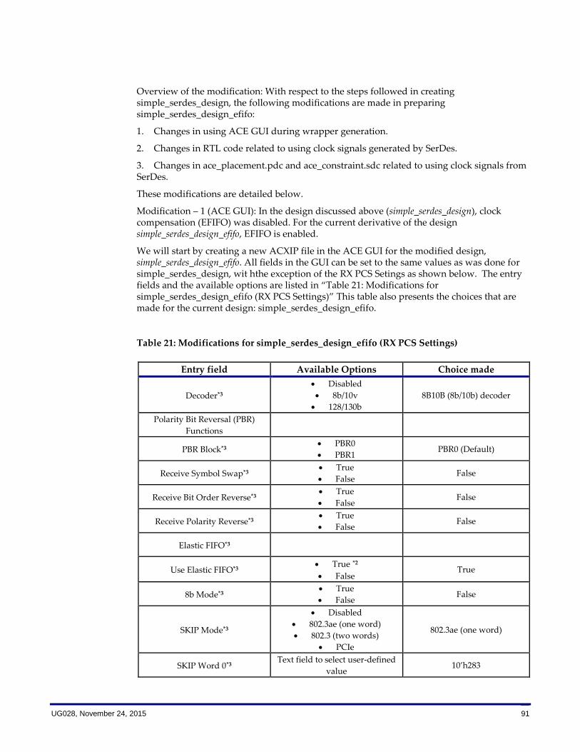
UG028, November 24, 2015 91
Overview of the modification: With respect to the steps followed in creating simple_serdes_design, the following modifications are made in preparing simple_serdes_design_efifo:
1. Changes in using ACE GUI during wrapper generation.
2. Changes in RTL code related to using clock signals generated by SerDes.
3. Changes in ace_placement.pdc and ace_constraint.sdc related to using clock signals from SerDes.
These modifications are detailed below.
Modification – 1 (ACE GUI): In the design discussed above (simple_serdes_design), clock compensation (EFIFO) was disabled. For the current derivative of the design simple_serdes_design_efifo, EFIFO is enabled.
We will start by creating a new ACXIP file in the ACE GUI for the modified design, simple_serdes_design_efifo. All fields in the GUI can be set to the same values as was done for simple_serdes_design, wit hthe exception of the RX PCS Setings as shown below. The entry fields and the available options are listed in “Table 21: Modifications for simple_serdes_design_efifo (RX PCS Settings)” This table also presents the choices that are made for the current design: simple_serdes_design_efifo.
Table 21: Modifications for simple_serdes_design_efifo (RX PCS Settings)
Entry field Available Options Choice made
Decoder*3
Disabled
8b/10v
128/130b
8B10B (8b/10b) decoder
Polarity Bit Reversal (PBR)
Functions
PBR Block*3 PBR0
PBR1 PBR0 (Default)
Receive Symbol Swap*3 True
False False
Receive Bit Order Reverse*3 True
False False
Receive Polarity Reverse*3 True
False False
Elastic FIFO*3
Use Elastic FIFO*3 True *2
False True
8b Mode*3 True
False False
SKIP Mode*3
Disabled
802.3ae (one word)
802.3 (two words)
PCIe
802.3ae (one word)
SKIP Word 0*3 Text field to select user-defined
value 10’h283

92 UG028, November 24, 2015
Entry field Available Options Choice made
Eanble ALT 0*3 True
False True
ALT SKIP Word 0*3
Text field to select user-defined
value (available only when
Enable ALT 1 is selected
10’h17C
SKIP Word 1*3 Text field to select user-defined
value
N/A since 802.3ae is chosen as
SKIP Mode
Eanble ALT 1*3 True
False
N/A since 802.3ae is chosen as
SKIP Mode
ALT SKIP Word 1*3
Text field to select user-defined
value (available only when
Enable ALT 0 is selected
N/A since 802.3ae is chosen as
SKIP Mode
SKIP Word 2*3 Text field to select user-defined
value
N/A since 802.3ae is chosen as
SKIP Mode
Eanble ALT 2*3 True
False
N/A since 802.3ae is chosen as
SKIP Mode
ALT SKIP Word 2*3
Text field to select user-defined
value (available only when
Enable ALT 2 is selected
N/A since 802.3ae is chosen as
SKIP Mode
Transition Density Checker
(TDC)
Enable Transition Density
Checker*3
True *1
False False
Max Count*3
Text field for user-defined value
(available only when TDC is
enabled)
N/A (TDC not enabled)
Max Count Scaling Factor*3
x1
x2
x4
x8
x16
N/A (TDC not enabled)
*1 If True is selected, the ACE GUI will add one input port (ch0_i_RX_tdc_clr) and one output port (ch0_o_tdc_det) to the wrapper RTL. This change is reflected in IP Diagram sub-window.
*2 When EFIFO enabled, four additional EFIFO related ports are added to wrapper (ch0_o_efifo_ovr_flw, ch0_o_efifo_skp_add, ch0_o_efifo_skp_del and ch0_o_efifo_und_run).
*3 Further descriptions on these functions are presented in Chapter-“PCS Blocks in the Receiver (RX)”
A snapshot of RX PCS Settings for the current derivative of the design is shown in “
Figure 41: PCS Settings for Receiver – Configurations for Decoder and Elastic FIFO”.

UG028, November 24, 2015 93
Figure 41: PCS Settings for Receiver – Configurations for Decoder and Elastic FIFO
Now, just as we did for the design without clock-compensation (simple_serdes_design), we can generate the design files from the ACE GUI for our design with clock compensation (simple_serdes_design_efifo).
Modification – 2 (RTL Code): The comma character that has previously been used for symbol alignment is used as EFIFO SKIP word in this derivative of the design. Therefore, no change is required for the data generation module (data_gen.v).
However, with clock compensation enabled, the aligned TX and RX clocks are available from the SerDes instance, as a single clock. Top-level design needs to be modified to reflect this. More specifically, in the baseline design simple_serdes_design, two clocks were generated by SerDes: ln0_TX_clk and ln0_RX_clk. These two clocks had respectively been used on the transmitter side (such as data generation) and on the receiver side (such as data check). In contrast, for the current derivative of the baseline design (simple_serdes_design_efifo), one clock .ch0_o_TX_data_clk is used as the clock from SerDes.
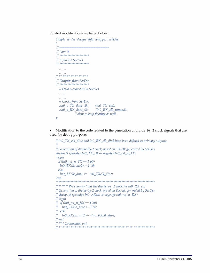
94 UG028, November 24, 2015
Related modifications are listed below:
Simple_serdes_design_efifo_wrapper iSerDes ( // ============================= // Lane 0 // ********************** // Inputs to SerDes // ********************** .. .. .. .. .. .. // ********************** // Outputs from SerDes // ********************** // Data received from SerDes .. .. .. .. .. .. // Clocks from SerDes .ch0_o_TX_data_clk (ln0_TX_clk), .ch0_o_RX_data_clk (ln0_RX_clk_unused), // okay to keep floating as well. );
• Modification to the code related to the generation of divide_by_2 clock signals that are used for debug purpose:
// ln0_TX_clk_div2 and ln0_RX_clk_div2 have been defined as primary outputs. // // Generation of divide-by-2 clock, based on TX-clk generated by SerDes always @ (posedge ln0_TX_clk or negedge ln0_rst_n_TX) begin if (ln0_rst_n_TX == 1'b0) ln0_TXclk_div2 <= 1'b0; else ln0_TXclk_div2 <= ~ln0_TXclk_div2; end // ************************************************************************ // ******* We comment out the divide_by_2 clock for ln0_RX_clk // Generation of divide-by-2 clock, based on RX-clk generated by SerDes // always @ (posedge ln0_RXclk or negedge ln0_rst_n_RX) // begin // if (ln0_rst_n_RX == 1'b0) // ln0_RXclk_div2 <= 1'b0; // else // ln0_RXclk_div2 <= ~ln0_RXclk_div2; // end // **** Commented out // ************************************************************************

UG028, November 24, 2015 95
Modification – 3 (placement and timing constraints): Since there is only one divide-by-two clock in this derivative of the design, we can remove the placement for ln0_RXclk_div2 from ace_placement.pdc.
Contents of the ace_constraints.sdc file can be copied from the ACE generated .sdc file except for the constraints related to the user-defined clocks (such as, reference clocks and snapshot clocks).
Design Bypassing PCS:
There are two modes for bypassing a PCS:
1. PCS Enabled mode: In this mode, PCS is not disabled, but all of the PCS modules are disabled. In other words, data (transmit and receive) will travel through the PCS components while bypassing them, as shown in “Figure 6: PCS Transmitter Block Overview”.
2. PCS Bypassed mode: In this mode, the PCS block is bypassed on both transmit and receive datapaths. This is shown in “Figure 6: PCS Transmitter Block Overview”.
Note: While creating the baseline design (simple_serdes_design), the PCS has been kept enabled while bypassing some PCS modules, such as EFIFO and deskew modules.
“Table 9: Latency across the PCS blocks” presents the latency that the data-path experiences for each of the above two modes:
With respect to the simple baseline design (simple_serdes_design) where some of the PCS modules are used, this derivative of the design will bypass PCS module individually (Mode-1 above) or will completely bypass the PCS block (Mode-2 above). This derivative of the baseline design is called simple_serdes_design_pcs_bypass. For this derivative, this section presents the derivatives with respect to the design flow used for creating the baseline design.
Specifications for this derivative are shown below.
Design name : simple_serdes_design_pcs_bypass Objective : Send data to SerDes and read-back using loopback. Data rate : 10.3125 Gbps Standard : Generic Number of lane : 1 Placement (lane to be used): Bottom-lane# 8 Ref. clock : 161.138125 Mhz Data width : 20 (Wrapper will use wide-bus to make data 40-bit wide) PCS blocks used : None
Mode – a: PCS modules are disabled Mode – b: PCS is disabled as a block.
No comma character required for transmit data since we are not using symbol alignment or deskew blocks.
Overview of the changes: Compared to the design flow used for the baseline design, the following changes are made for simple_serdes_design_pcs_bypass:
1. Change in using ACE GUI during wrapper generation.
2. Change in RTL code.
Note: There will be no change required for placement-constraint (ace_placement.pdc) and timing-constraint (ace_constraint.sdc) when compared to the files used for the baseline design.

96 UG028, November 24, 2015
Note: Although the PCS modules are disabled, the SerDes will still generate two clocks for transmit and receive ends (from PMA). Unlike the design with EFIFO enabled (simple_serdes_design_efifo), these two clocks are not aligned.
The changes for this derivative of the design are presented below.
Modification – 1 (ACE GUI):
Mode – a (Bypassing PCS Modules without Disabling PCS): While generating GUI wrapper for this derivative, we need to disable the followings:
1. 8b/10b encoder module in RX PCS Settings window,
2. Symbol alignment module in RX PCS Symbol Alignment window, and
3. 8b/10b decoder in TX PCS Settings window.
Details on these windows have been presented while explaining the design flow for the baseline design.
Mode – b (Disabling PCS that essentially disables all PCS blocks): In this mode, the PCS block is completely disabled.
This can be done by disabling the PCS from ACE GUI as shown in
Figure 42: Disabling PCS from ACE GUI. Please note that for the baseline design simple_serdes_design, the box was left unchecked (Figure 31: PCS Settings Window – First page).
Modification – 2 (Design RTL): With respect to the sample design (simple_serdes_design), this variant with PCS bypassed will require only one change in top-level design due to the fact that comma character is not longer required. Corresponding changes in the module data_generation is presented below:
module data_generation ( input clk, input rst_n, input data_gen_en, output [39:0] data_out ); always @ (posedge clk) begin if (rst_n == 1'b0) data_out <= 40’b0; // *** Comment out the comma-character generation // *** data_out <= {10'h000,10'h1BC,10'h000,10'h1BC}; else if (data_gen_en == 1’b1) // when data-generation enabled, i.e. TX_ready from SerDes is up // *** Logic for data-generation goes here, such as PRBS-7 *** else data_out <= 40’b0; // *** Comment out the comma-character generation // ***data_out <= {10'h000,10'h1BC,10'h000,10'h1BC}; end endmodule

UG028, November 24, 2015 97
Note: When compared with the sample design (simple_serdes_design), no change is required in ace_placement.pdc or in ace_constraint.sdc files for this derivative (simple_serdes_design_pcs_bypassed). The instantiation of the SerDes wrapper will remain same.
Figure 42: Disabling PCS from ACE GUI
Bypassing PCS by Manually Overriding Corresponding Register
This section presents use an alternative approach for bypassing PCS through the Advanced section in ACE GUI. This is presented for demonstration purpose only.
The PCS blocks can be bypassed by modifying the value stored in the PCS register 17A. More specifically, the bit-4 of the PCS register 17A needs to be set at 1’b1 to bypass the PCS block.
The values of the PCS/PMA registers can be overridden by using the Advanced section of the ACE GUI. The user can reach Advanced section by selecting the link in the Outline window (“ Figure 24: Outline Window”).
Clicking Next button will bring the page titled Register Settings – Lane 0 as shown in “Figure 43: Modifying Register Settings from ACE GUI”. This page has several fields:
1. Start Address, End Address and Function. These fields are used to search for a specific PCS register. The hexadecimal address is used for both PCS and PMA registers.
2. A table displaying the list of AHB addresses (1st column: AHB Address) and the corresponding values set by ACE (3rd column: Value). The 2nd column (Override Value) will display the values that are entered as overriding value, such as bit-4 of Reg17A.
3. Two text boxes for AHB Address and Override Value. To enter the value that will override the default value of a register. Both of these entries need to be in hexadecimal format.
4. A table that shows the details on each bit for the register that corresponds to the address typed in AHB Address text-field.
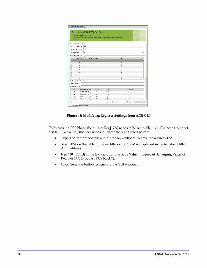
98 UG028, November 24, 2015
Figure 43: Modifying Register Settings from ACE GUI
To bypass the PCS block, the bit-4 of Reg[17A] needs to be set to 1’b1, i.e., 17A needs to be set at 8’h10. To do that, the user needs to follow the steps listed below:
Type 17A in start address and hit tab on keyboard to have the address 17A.
Select 17A on the table in the middle so that ‘17A’ is displayed in the text-field titled AHB address.
type ‘10’ (8’h10) in the text-field for Override Value (“Figure 44: Changing Value of Register 17A to bypass PCS block”).
Click Generate button to generate the GUI wrapper.
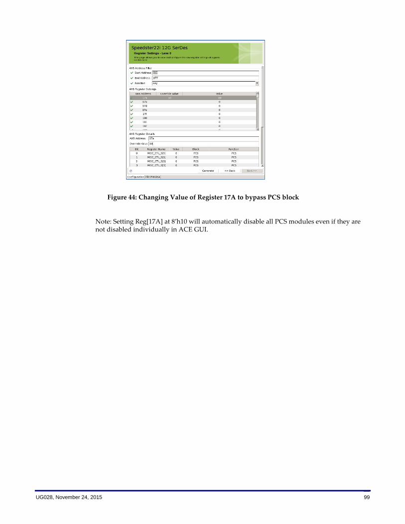
UG028, November 24, 2015 99
Figure 44: Changing Value of Register 17A to bypass PCS block
Note: Setting Reg[17A] at 8’h10 will automatically disable all PCS modules even if they are not disabled individually in ACE GUI.

100 UG028, November 24, 2015
Dynamic Read/Write of SerDes Registers via SBUS
This chapter broadly categorizes the PMA and PCS registers into:
1. Static registers
2. Dynamic registers
While the static registers are hardcoded into ACE generated GUI, the dynamic registers can be modified runtime. This chapter details the macros that can be used to modify the dynamic PCS/PMA registers.
Typically, SerDes registers are programmed during FPGA configuration, and there is no need to program them dynamically. One common case where registers need to be programmed dynamically is to set loopback mode.
In this chapter, we first present the overview of the SerDes register access through SBUS. We then present a micro-controller that executes one or more sequences of SBUS register accesses. Finally, we present an example of existing ACE macros for using SBUS interface; the example presents the case where the user wants to set the SerDes loopback mode.
Overview
The Serdes has a serial interface, called SBUS, through which the user design can read and write internal registers. The ACX_SERDES_SBUS_IF module provides parallel-to-serial conversion for this interface. (Other I/O ring components have an SBUS interface as well.)
To enable SerDes register access through SBUS, the user needs to use the following in the code.
`include "speedster22i/macros/ACX_SERDES_SBUS_IF.v"
Alternatives for using SBUS interface for SerDes register access:
There are several ways of using SBUS interface for SerDes register access:
The user can use the ACX_SERDES_SBUS_IF module that is a relatively low-level interface.
Rather than using ACX_SERDES_SBUS_IF module, wrappers for common configurations can be created using ACX_SERDES_REG_CTRL.
For some purposes, ACE library provides wrapper macros. For instance, for the common case of setting loopback mode using SBUS interface, the user can use the macro ACX_SERDES_LOOPBACK_CTRL; this macro automatically configures loopback mode once the SerDes is ready.
Each of the above requires using SBUS interface to access PMA/PCS registers. The BitPorter perspective in the Ace GUI has a JTAG Browser tab, which allows reading and writing the SerDes register values interactively through the JTAG interface. This gives access to the same registers as the SBUS interface.
Note: Both ACX_SERDES_REG_CTRL and ACX_SERDES_LOOPBACK_CTRL calls the low-level ACX_SERDES_SBUS_IF under the hood.

UG028, November 24, 2015 101
ACX_SERDES_SBUS_IF Module
The connection diagram for ACX_SERDES_SBUS_IF is shown in “ Figure 45: Disabling PCS Decoder (default ACE Setting)”.
Figure 45: Disabling PCS Decoder (default ACE Setting)
The code below presents the port definitions in ACX_SERDES_SBUS_IF module
module ACX_SERDES_SBUS_IF ( input sbus_clk, input rstn, input sbus_sw_rst, // active-high; may be tied low // serdes connections input [1:0] from_sbus_data, input from_sbus_ack, output [1:0] to_sbus_data, output to_sbus_req, output to_sbus_sw_rst, // parallel interface input i_reg_rw_req, // rising edge starts action input i_reg_write, // request is 'write' input i_reg_pma, // address is pma address input [15:0] i_reg_address, // 16-bit pcs or pma address input [7:0] i_reg_wr_data, // data for write output [7:0] o_reg_rd_data, // data from read (latch when o_reg_rdwr_valid) output reg o_reg_rdwr_valid // action finished (high for one cycle) );

102 UG028, November 24, 2015
The Ports of ACX_SERDES_SBUS_IF Module:
The signals (ports) shown in “Figure 44: Changing Value of Register 17A to bypass PCS block” and “The Ports of ACX_SERDES_SBUS_IF Module:” are detailed now.
General signals:
Port sbus_clk: There should be one ACX_SERDES_SBUS_IF instance per SerDes lane. For each lane, a clock signal is required to drive both the SerDes (input ports ch0_i_sbus_clk etc.) and ACX_SERDES_SBUS_IF (input port sbus_clk). The sbus_clk may be shared with multiple Serdes lanes. The sbus_clk is normally generated by a PLL, and, for practical reasons, should be 50MHz or less. You cannot use the RX or TX clock for this.
Port rstn: The active-low rstn signal must be asserted briefly at start-up to initialize the interface. Deassertion should be synchronous to sbus_clk.
Port sbus_sw_rst: The synchronous sbus_sw_rst signal is optional. It can be used with a timeout counter: when a timeout occurs, sbus_sw_rst is asserted (active-high) to reset the internal state machine to its start state. However, unless there is some internal failure, no timeout should occur. If this mechanism is not needed, the sbus_sw_rst pin can be tied to GND. (If you want to add a timeout, allow at least 64 cycles per read or write.)
SerDes signals:
SerDes interface ports – from_sbus and to_sbus: As shown in “Figure 46: Connections for ACX_SERDES_LOOPBACK_CTRL”, the from_sbus inputs must be driven by the matching SerDes outputs, and the to_sbus output must drive the matching SerDes inputs. The user will also find an example of this constraint when we will present the example of setting loopback mode using SBUS interface.
Parallel Interface signals:
Ports i_reg_rw_req and o_reg_rdwr_valid: A register read or write is triggered by a rising edge on i_reg_rw_req, and completion is signaled by o_reg_rdwr_valid.
Port i_reg_write and i_reg_wr_data: The i_reg_write input indicates whether the requested action is a read or a write. For a write, the 8-bit register value is passed via i_reg_wr_data. All inputs (data and address) are registered internally by the interface.
Ports i_reg_pma and i_reg_address: The SerDes has two sets of registers, PCS registers and PMA registers. Both have their own 16-bit address space (not all addresses are used). If i_reg_pma is high, i_reg_address is a PMA address; otherwise it is a PCS address.
Port o_reg_rdwr_valid and o_reg_rd_data: Completion of a read or write is signaled by o_reg_rdwr_valid high. This signal is high for only one cycle. For a read, the register value is available on o_reg_rd_data, but only for the cycle where o_reg_rdwr_valid is high. You can latch this signal as:
if (!i_reg_write && o_reg_rdwr_valid) my_reg <= o_reg_rd_data;
Note: A write operation writes all 8 bits of the register. To modify only selected bits, you need to perform a read-modify-write: read the register value, modify the value locally, then write the result back.
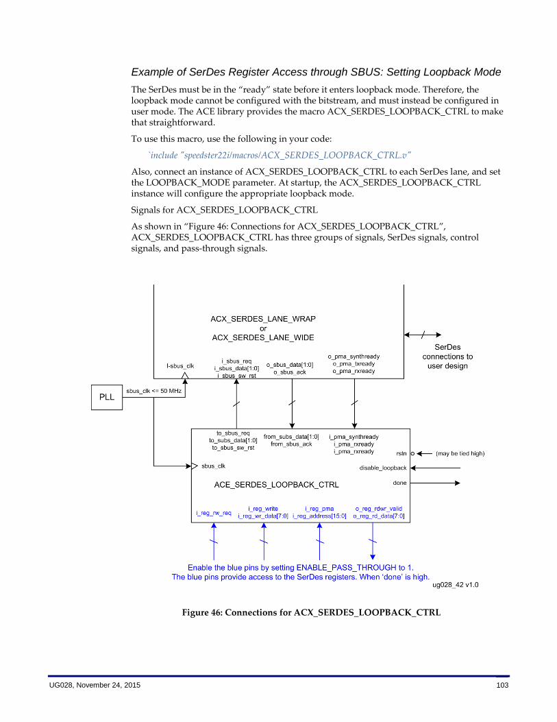
UG028, November 24, 2015 103
Example of SerDes Register Access through SBUS: Setting Loopback Mode
The SerDes must be in the “ready” state before it enters loopback mode. Therefore, the loopback mode cannot be configured with the bitstream, and must instead be configured in user mode. The ACE library provides the macro ACX_SERDES_LOOPBACK_CTRL to make that straightforward.
To use this macro, use the following in your code:
`include "speedster22i/macros/ACX_SERDES_LOOPBACK_CTRL.v"
Also, connect an instance of ACX_SERDES_LOOPBACK_CTRL to each SerDes lane, and set the LOOPBACK_MODE parameter. At startup, the ACX_SERDES_LOOPBACK_CTRL instance will configure the appropriate loopback mode.
Signals for ACX_SERDES_LOOPBACK_CTRL
As shown in “Figure 46: Connections for ACX_SERDES_LOOPBACK_CTRL”, ACX_SERDES_LOOPBACK_CTRL has three groups of signals, SerDes signals, control signals, and pass-through signals.
Figure 46: Connections for ACX_SERDES_LOOPBACK_CTRL

104 UG028, November 24, 2015
SerDes signals
Sbus_clk and ready signals: The sbus_clk and ready signals must be connected between SerDes lane and ACX_SERDES_LOOPBACK_CTRL. The sbus_clk must be connected to both SerDes lane and ACX_SERDES_LOOPBACK_CTRL. The sbus_clk may be shared with multiple SerDes lanes. The sbus_clk is normally generated by a PLL, and, for practical reasons, should be 50MHz or less. You cannot use the RX or TX clock for this.
Control signals
Signal done: When ACX_SERDES_LOOPBACK_CTRL has finished configuring the Serdes, it raises done.
Signal disable_loopback: The disable_loopback input can be used to dynamically disable loopback mode. Asserting and de-asserting rstn will enable loopback mode again, as will a reset of the SerDes.
Note: If for some reason you want to re-apply the Serdes hard reset (i_rst_hard_n) after the design has been running for a while, then you must first disable loopback, using disable_loopback. When the Serdes comes out of hard reset, the loopback mode will automatically be re-enabled.
Pass-through signals:
Most designs don't need the pass-through signals.
Loopback Modes
Please refer to Section - Loopback Modes for the valid loopback modes available with Achronix FPGA.
Example Code wire loopback_done; wire [1:0] from_sbus_data, to_sbus_data; wire from_sbus_ack, to_sbus_req, to_sbus_sw_rst; wire pma_synthready, pma_TXready, pma_RXready; ACX_SERDES_LOOPBACK_CTRL #( .LOOPBACK_MODE(`LPBK_TX_RX_PMA_INTERNAL), .ENABLE_PASS_THROUGH(0) ) loopback_ch0 ( .sbus_clk(sbus_clk), .rstn(1'b1), .disable_loopback(1'b0), .done(loopback_done), // serdes connections .from_sbus_data(from_sbus_data), .from_sbus_ack(from_sbus_ack), .to_sbus_data(to_sbus_data), .to_sbus_req(to_sbus_req), .to_sbus_sw_rst(to_sbus_sw_rst), .i_pma_synthready(pma_synthready), .i_pma_TXready(pma_TXready),
UG028, November 24, 2015 105
.i_pma_RXready(pma_RXready), ); // Use the IP Configuration Perspective in Ace to generate a Serdes wrapper gui_generated_serdes_wrapper iSERDES ( .ch0_i_sbus_clk (sbus_clk), .ch0_i_sbus_data (to_sbus_data), .ch0_i_sbus_req (to_sbus_req), .ch0_i_sbus_sw_rst (to_sbus_sw_rst), .ch0_o_sbus_ack (from_sbus_ack), .ch0_o_sbus_data (from_sbus_data), .ch0_o_pma_RXready (pma_RXready), .ch0_o_pma_TXready (pma_TXready), .ch0_o_pma_synthready (pma_synthready) .... );
SerDes Registers
Please contact customer support for PMA and PCS register description
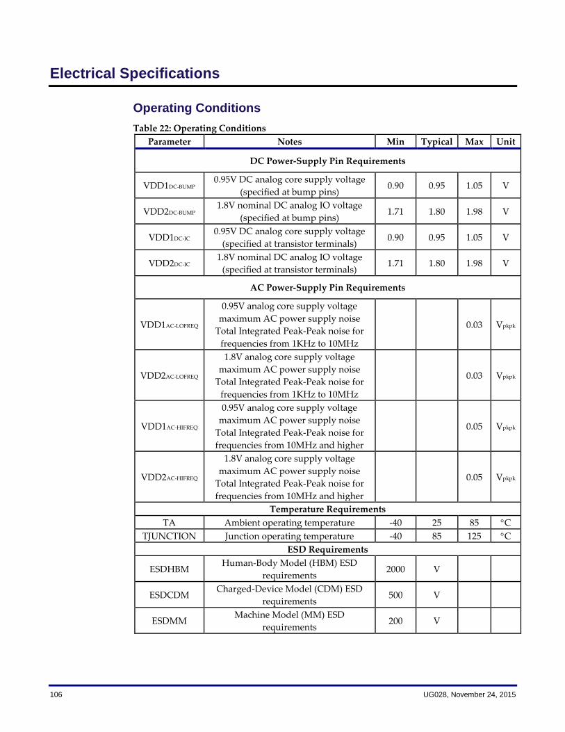
106 UG028, November 24, 2015
Electrical Specifications
Operating Conditions
Table 22: Operating Conditions
Parameter Notes Min Typical Max Unit
DC Power-Supply Pin Requirements
VDD1DC-BUMP 0.95V DC analog core supply voltage
(specified at bump pins) 0.90 0.95 1.05 V
VDD2DC-BUMP 1.8V nominal DC analog IO voltage
(specified at bump pins) 1.71 1.80 1.98 V
VDD1DC-IC 0.95V DC analog core supply voltage
(specified at transistor terminals) 0.90 0.95 1.05 V
VDD2DC-IC 1.8V nominal DC analog IO voltage
(specified at transistor terminals) 1.71 1.80 1.98 V
AC Power-Supply Pin Requirements
VDD1AC-LOFREQ
0.95V analog core supply voltage
maximum AC power supply noise
Total Integrated Peak-Peak noise for
frequencies from 1KHz to 10MHz
0.03 Vpkpk
VDD2AC-LOFREQ
1.8V analog core supply voltage
maximum AC power supply noise
Total Integrated Peak-Peak noise for
frequencies from 1KHz to 10MHz
0.03 Vpkpk
VDD1AC-HIFREQ
0.95V analog core supply voltage
maximum AC power supply noise
Total Integrated Peak-Peak noise for
frequencies from 10MHz and higher
0.05 Vpkpk
VDD2AC-HIFREQ
1.8V analog core supply voltage
maximum AC power supply noise
Total Integrated Peak-Peak noise for
frequencies from 10MHz and higher
0.05 Vpkpk
Temperature Requirements
TA Ambient operating temperature -40 25 85 C
TJUNCTION Junction operating temperature -40 85 125 C
ESD Requirements
ESDHBM Human-Body Model (HBM) ESD
requirements 2000 V
ESDCDM Charged-Device Model (CDM) ESD
requirements 500 V
ESDMM Machine Model (MM) ESD
requirements 200 V

UG028, November 24, 2015 107
Transmitter
Table 23: DC and AC Switching Characteristics
Parameter Description Min Typical Max Unit
Output Eye Specification
VTX-DIFF-PKPK Backporch Transmit Amplitude 400 1500 mVdiff-
pkpk
VTX-EYE-PKPK Transmit Eye Voltage Opening 400 1200 mVdiff-
pkpk
DTX-N+1-DEEMP N+1 precursor Tap De-Emphasis 0 2.5 dB
DTX-N-1-DEEMP N-1 postcursor Tap De-Emphasis 0 8.5 dB
DTX-N-2-DEEMP N-2 postcursor Tap De-Emphasis 0 2.5 dB
TTX-SLEW Rise/Fall Time 30 120 ps
TTX-DDJ
Transmit Dependant Jitter (Inter-
Symbol Interference) at 8Gbps.
Includes package model
0.05 UIpkpk
TTX-PJ
Transmit Periodic Jitter. Assumes a
1st order high pass jitter
measurement filter with a cutoff of
FBAUD/ FGPLL = NGPLL
0.05 UIpkpk
TTX-RJ
Transmit Total Peak-Peak Random
Jitter (assumes 14TXRJ-RMS). Assumes
a 1st order high pass jitter
measurement filter with a cutoff of
FBAUD/ FGPLL = NGPLL
0.15 UIpkpk
TTX-TJ
Transmit Total Peak-Peak Jitter
(Assumes TTX-TJ = TTX-DDJ + TTX-PJ + TTX-
RJ). Assumes a 1st order high pass
jitter measurement filter with a cutoff
of FBAUD/ FGPLL = NGPLL
0.25 UIpkpk
NGPLL
F3dB cutoff frequency for the 1st
Order High-Pass Jitter Measurement
Filter.
Defined as the ratio of the F3DB cutoff
frequency, to the data rate
1667 FBAUD/
FGPLL
VTX-CM-PKPK-AC Pk-PK AC Common Mode Voltage
Variation 100 mV
VTX-CM-RMS-AC RMS AC Common Mode Voltage
Variation 20 mV
Transmitter DC Impedance
ZTX-DIFF-DC Transmitter Output Differential DC
Impedance 80 100 120
ZTX-CM-DC Transmitter Output Common-Mode
DC Impedance 20 25 30

108 UG028, November 24, 2015
Parameter Description Min Typical Max Unit
ZTX-DIFF-HIZ Transmitter Output Differential DC
Impedance in Squelch Mode >2k
ZTX-CM-HIZ Transmitter Output Common-Mode
DC Impedance in Squelch Mode >500
Transmitter Return Loss
ZRL-DIFF-DC Transmitter Differential DC Return
Loss -14 dB
ZRL-DIFF-NYQ Transmitter Differential Return Loss
at Nyquist Frequency (FBAUD/2) -6 dB
ZRL-CM-DC Transmitter Common-Mode DC
Return Loss -6 dB
ZRL-CM-NYQ Transmitter Common-Mode Return
Loss at Nyquist Frequency (FBAUD) -4 dB
Electrical Idle
VTX-IDLE Idle Output Voltage 20 mVpkpk
VCM-DELTA-
SQUELCH
Maximum Common-Mode Step
Entering/Exiting Squelch Mode 50 mV
TTX-IDLE-
LATENCY Latency Entering/Exiting Idle 8 ns
Receiver Detect
VTX-RCV-DETECT Voltage change allowed during
receiver detection 600 mV
Table 24: Jitter
Standard Total Jitter (TJ) Deterministic
Jitter (DJ) Units Compliant?
PCI Express Gen1/Gen2/Gen3
0.25 0.15 UIp-p
Yes
GigE – SGMII 0.375 0.125 UIp-p Yes
10G Ethernet – XAUI 0.35 0.17 UIp-p Yes
CEI 6G – SR/LR 0.3 0.15 UIp-p Yes
CEI 11G – SR/MR/LR 0.3 0.15 UIp-p Yes
Fibre Channel (FC-1, FC-2, FC-4, FC-8)
0.24 0.12 UIp-p Yes
SATA (Gen1, Gen2) 0.37 0.15 UIp-p Yes

UG028, November 24, 2015 109
Table 25: Return Loss
Standard Differential DC return
loss
Differential return loss at FBAUD/2
Common mode DC
return loss
Common mode return
loss at FBAUD/2
Units Compliant?
PCIe Gen1 10 10 6 6 dB Yes
PCIe Gen2 10 8 6 6 dB Yes
PCIe Gen3 dB Yes
XAUI 10 5.9 -- -- dB Yes
CEI 6G – SR/LR
8 8 6 6 dB Yes
FC-1 12 12 12 11.1 dB Yes
FC-2 12 9.5 12 7.5 dB Yes
FC-4 12 6 12 4 dB Yes
SATA (Gen1, Gen2)
14 6 5 2 dB Yes
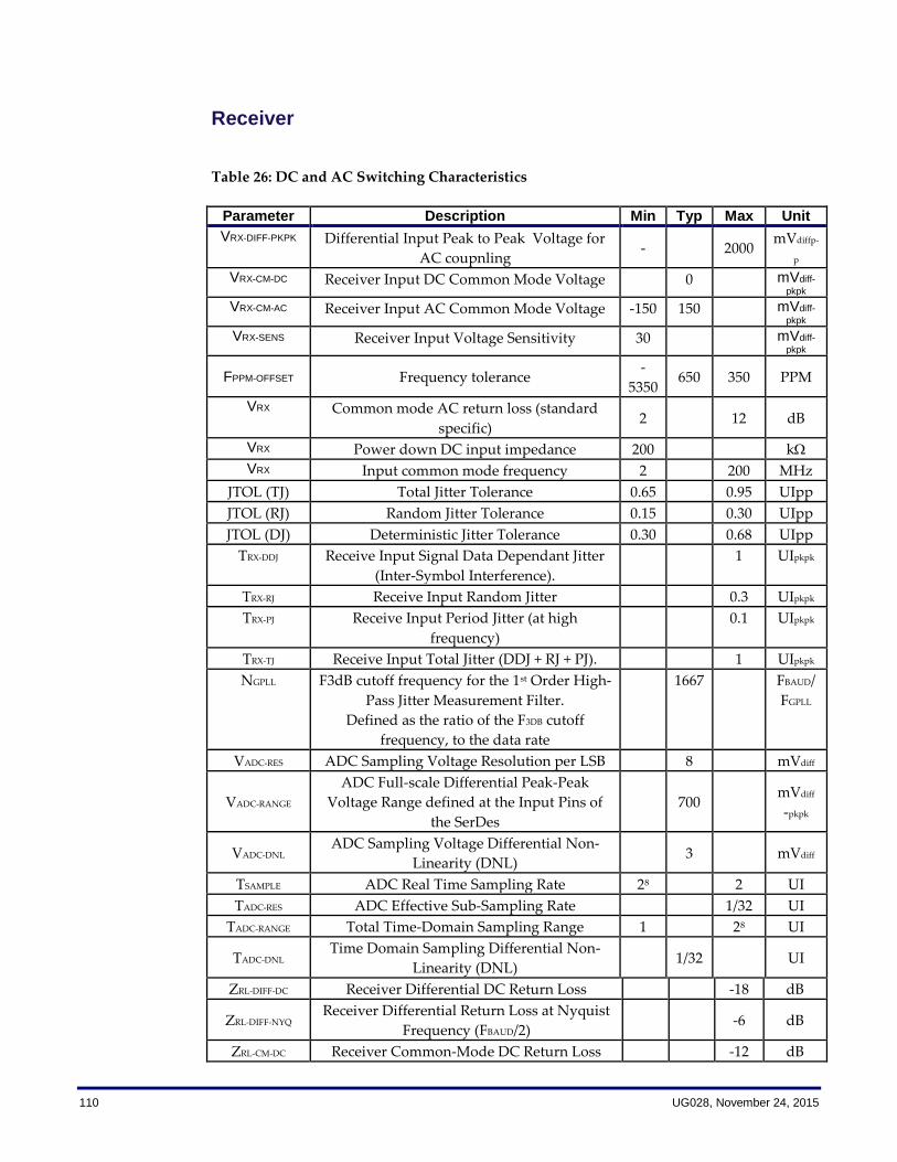
110 UG028, November 24, 2015
Receiver
Table 26: DC and AC Switching Characteristics
Parameter Description Min Typ Max Unit
VRX-DIFF-PKPK
Differential Input Peak to Peak Voltage for
AC coupnling -
2000
mVdiffp-
p
VRX-CM-DC Receiver Input DC Common Mode Voltage 0 mVdiff-
pkpk VRX-CM-AC Receiver Input AC Common Mode Voltage -150 150 mVdiff-
pkpk
VRX-SENS Receiver Input Voltage Sensitivity 30 mVdiff-
pkpk
FPPM-OFFSET Frequency tolerance -
5350 650 350 PPM
VRX Common mode AC return loss (standard
specific) 2
12 dB
VRX Power down DC input impedance 200 k
VRX Input common mode frequency 2 200 MHz
JTOL (TJ) Total Jitter Tolerance 0.65 0.95 UIpp
JTOL (RJ) Random Jitter Tolerance 0.15 0.30 UIpp
JTOL (DJ) Deterministic Jitter Tolerance 0.30 0.68 UIpp
TRX-DDJ Receive Input Signal Data Dependant Jitter
(Inter-Symbol Interference).
1 UIpkpk
TRX-RJ Receive Input Random Jitter 0.3 UIpkpk
TRX-PJ Receive Input Period Jitter (at high
frequency)
0.1 UIpkpk
TRX-TJ Receive Input Total Jitter (DDJ + RJ + PJ). 1 UIpkpk
NGPLL F3dB cutoff frequency for the 1st Order High-
Pass Jitter Measurement Filter.
Defined as the ratio of the F3DB cutoff
frequency, to the data rate
1667 FBAUD/
FGPLL
VADC-RES ADC Sampling Voltage Resolution per LSB 8 mVdiff
VADC-RANGE
ADC Full-scale Differential Peak-Peak
Voltage Range defined at the Input Pins of
the SerDes
700 mVdiff
-pkpk
VADC-DNL ADC Sampling Voltage Differential Non-
Linearity (DNL) 3 mVdiff
TSAMPLE ADC Real Time Sampling Rate 28 2 UI
TADC-RES ADC Effective Sub-Sampling Rate 1/32 UI
TADC-RANGE Total Time-Domain Sampling Range 1 28 UI
TADC-DNL Time Domain Sampling Differential Non-
Linearity (DNL) 1/32 UI
ZRL-DIFF-DC Receiver Differential DC Return Loss -18 dB
ZRL-DIFF-NYQ Receiver Differential Return Loss at Nyquist
Frequency (FBAUD/2) -6 dB
ZRL-CM-DC Receiver Common-Mode DC Return Loss -12 dB

UG028, November 24, 2015 111
Parameter Description Min Typ Max Unit
ZRL-CM-NYQ Receiver Common-Mode Return Loss at
Nyquist Frequency (FBAUD/2) -4 dB
Receiver DC Impedance
RDIFF-DC DC Differential Receive Impedance 80 100 110 Ohm
RCM-DC DC Common-Mode Receive Impedance 20 25 27.5 Ohm
RDIFF-HIZ-POS Differential Receive High Impedance for
Input Voltage from 0V to 200mV 200k Ohm
RCM-HIZ-POS Common-mode Receive High Impedance for
Input Voltage from 0V to 200mV 50k Ohm
RDIFF-HIZ-NEG Differential Receive High Impedance for
Input Voltage from -150mV to 0mV 4k Ohm
RCM-HIZ-NEG Common-mode Receive High Impedance for
Input Voltage from -150mV to 0mV 1k Ohm
Receiver Signal Detection
VIDLE-THRESH Receiver Signal Detect Input Voltage
Threshold 75 120 175
mVdiff-
pkpk
TSIGDET-ATTACK Signal Detect Valid Signal Attack Time
(Turn-on time) in SATA mode 15 Ns
TSIGDET-DECAY Signal Detect Valid Signal Decay Time (Turn-
off time) in SATA mode 15 ns
TSIGDET-ATT-
DECAY-MIS
Signal Detect Attack / Decay Time Mismatch
in SATA mode 5 ns
Equalizer/Re-timer Mode Specifications
TRCLK-DJ
Recovered Clock Deterministic Jitter
(in lock-to-data and in lock-to-reference
modes)
0.075 UIpkpk
TRCLK-RJ
Recovered Clock Random Jitter (at 1E-12
BER)
(in lock-to-data and in lock-to-reference
modes)
0.112 UIpkpk
NRCLK-GPLL
F3dB cutoff frequency for the 1st Order High-
Pass Jitter Measurement Filter.
Defined as the ratio of the F3DB cutoff
frequency, to the data rate
1667 FBAUD/
FGPLL
Repeater Receiver Input Eye Specification
VRX-DIFF-PKPK Receiver Input Differential Peak-Peak Voltage 250 2000 mVdiff-
pkpk
VRX-CM-DC Receiver Input DC Common Mode Voltage 0 mVdiff-
pkpk
VRX-CM-AC Receiver Input AC Common Mode Voltage -150 150 mVdiff-
pkpk

112 UG028, November 24, 2015
Parameter Description Min Typ Max Unit
VRX-SENS
Receiver Input Voltage Sensitivity Under the
Following Conditions:
50inch of FR4
6.25Gbps
PRBS7 data pattern
40 50 mVdiff-
pkpk
TRX-DDJ Receive Input Signal Data Dependant Jitter
(Inter-Symbol Interference). 1 UIpkpk
TRX-TJ Receive Input Signal Total Jitter (Inter-Symbol
Interference). 1 UIpkpk
NGPLL
F3dB cutoff frequency for the 1st Order High-
Pass Jitter Measurement Filter.
Defined as the ratio of the F3DB cutoff
frequency, to the data rate
1667 FBAUD/
FGPLL
Eye Diagram
This section describes the RX eye diagram specifications of the SerDes. The specifications include required input voltage swing and receiver jitter tolerance requirements. The eye template used is shown in “Figure 47: Receiver (RX) Eye Diagram Specification”.
Figure 47: Receiver (RX) Eye Diagram Specification
Table 27: Receiver (RX) Eye Diagram Specification
Standard X1 (UI) X2 (UI) 2xVp-min
(mV) 2xVp-max
(mV)
PCIe 1.0 0.3 0.5 175 1200
PCIe 2.0 0.3 0.5 120 1200
sGMII 0.25 0.5 675 1725
GigE 0.355 0.5 200 2000
XAUI 0.325 0.4 200 1600
OIF CEI 6G – SR 0.3 0.5 125 750
OIF CEI 6G – LR 0.475 0.5 N/A 1200

UG028, November 24, 2015 113
Standard X1 (UI) X2 (UI) 2xVp-min
(mV) 2xVp-max
(mV)
FC-1 0.33 0.5 275 2000
FC-2 0.35 0.5 275 2000
FC-4 0.33 0.5 275 2000
SATA Gen1 0.325 0.5 275 1600
SATA Gen2 0.325 0.5 275 1600
SAS Rev5 0.325 0.5 275 1600
Table 28: Return Loss
Reference Clock
The electrical specifications for the reference clock are summarized in the following tables
Table 29: Reference Clock Electrical Speficiations
Parameter Description Min Typical Max Unit
FREF Reference clock operating frequency
range 50 250 MHz
TREF Reference clock operating frequency
range 4 20 ns
TREF-DUTY Duty Cycle 40 50 60 %
TREF-RISE/FALL Rise and falling edge rate 0.2 TREF
TREF-SINGLEEND- Skew between REFCLKP and REFCLKM 10 ps
Standard Differential DC return
loss
Differential return loss at FBAUD/2
Common mode DC return loss
Common mode return
loss at FBAUD/2 Units
PCIe Gen1 10 10 6 6 dB
PCIe Gen2 10 8 6 6 dB
XAUI 10 10 6 6 dB
CEI 6G – SR 8 8 6 6 dB
CEI 6G-LR 8 8 6 6 dB
FC-1 12 12 12 12 dB
FC-2 12 9.5 12 10.5 dB
FC-4 12 6 12 7 dB
SATA (Gen1, Gen2)
18 8 5 2 dB

114 UG028, November 24, 2015
Parameter Description Min Typical Max Unit
SKEW
TREF-PPM-ERROR Reference Clock Frequency Error -5350 +350 ppm
ZREF-SINGLEEND-DC Reference Clock Input Impedance –
Terminated Mode 40 50 60
ZREF-DIFF-DC Reference Clock Input Impedance – High
Impedance Mode >200k
VREF-DIFF
Input Differential Voltage - PCIe 0.15 V
Input Differential Voltage - LVDS 0.25 0.4 V
Input Differential Voltage - LVPECL 0.525 0.95 V
VREF-CM
Input Common Mode Voltage - PCIe 0.25 0.55 V
Input Common Mode Voltage - LVDS 1 1.4 V
Input Common Mode Voltage - LVPECL 1.84 2.1 V
TREF-RMS-MAX
Total Integrated RMS Phase Noise for the
band of frequency ranging from 12kHz to
20MHz
0.7 psRMS
Jitter Specification
Table 30: Reference Clock Jitter Specification
Reference Clock Parameter Typ Max Unit
Suggested RMS phase jitter at 333.3 MHz (12KHz to 20
MHz) 0.8 400 ps rms
Suggested cycle to cycle jitter at 333.3 MHz 51 ps p-p
SATA/SAS: cycle to cycle jitter 112 ps p-
p
SATA/SAS: deterministic jitter 40 ps p-p
FC: cycle-to-cycle jitter RMS 6 ps p-p
FC: deterministic jitter 5 ps p-p
PCI-Express Gen1: cycle to cycle jitter 150 ps p-p
PCI-Express Gen2: 10KHz – 1.5 MHz bandwidth 7.5 ps rms
PCI-Express Gen2: 1.5MHz – 2.5GHz bandwidth 4.0 ps rms
XFI: RMS random jitter (up to 100MHz) 10 ps rms

UG028, November 24, 2015 115
Revision History
The following table shows the revision history for ths document.
Date Version Revisions
3/29/2013 1.0 First customer release
4/22/2013 1.1 Updated ref clk frequencies
5/21/2013 1.2 Corrected some formatting issues
4/30/2014 1.3 Complete overhaul of the document
6/3/2014 2.0 Reformatted. Updated images, major updates
7/1/2014 2.1 Further input from Engineering
11/24/2015 2.2 Added in SFF-8431 support for SFI