Embed Size (px)
DESCRIPTION
to control the speed of a dc motor
Citation preview

i
A Project Report Submitted to the
ELECTRICAL ENGINEERING
DEPARTMENT
AS TERM WORK FOR THE SUBJECT
PROJECTPROJECTPROJECTPROJECT
OF SEMESTER VIII
OF
BE (Electrical)
GUIDED BY PREPARED BY Lect HITARTH BUCH
Mr RAHUL PARMAR Mr SUSHIL RATHOD Mr HARSHAD PATEL Mr CHETAN KOTHIYA Mr VIKRAMSINH MALIVAD
ELECTRICAL ENGINEERING DEPARTMENT
L E COLLEGE MORBI-2 SAURASHTRA UNIVERSITY RAJKOT
YEAR 2007
ii
LUKHDHIRJI ENGINEERING COLLEGE
MORBI -363642
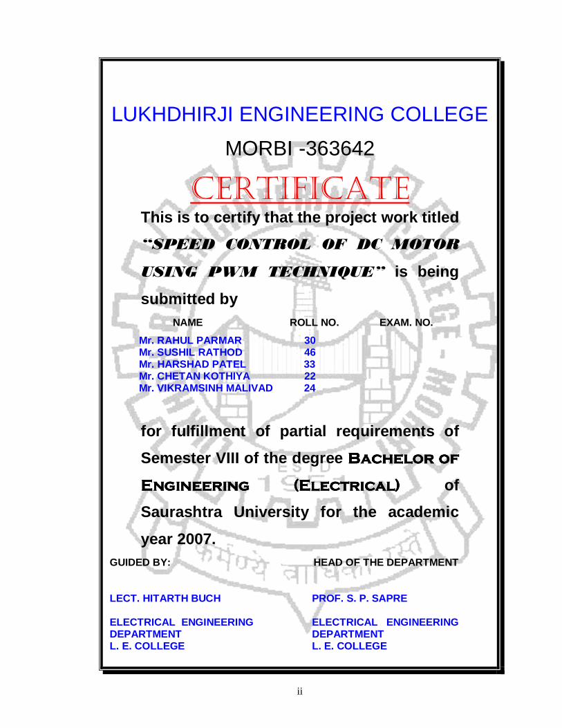
CERTIFICATE This is to certify that the project work titled
ldquoSPEED CONTROL OF DC MOTOR
USING PWM TECHNIQUErdquo is being
submitted by NAME ROLL N O EXAM NO
Mr RAHUL PARMAR 30 Mr SUSHIL RATHOD 46 Mr HARSHAD PATEL 33 Mr CHETAN KOTHIYA 22 Mr VIKRAMSINH MALIVAD 24
for fulfillment of partial requirements of
Semester VIII of the degree BachelorBachelorBachelorBachelor of of of of
Engineering (ElectEngineering (ElectEngineering (ElectEngineering (Electrrrricalicalicalical)))) of
Saurashtra University for the academic
year 2007 GUIDED BY
HEAD OF THE DEPARTMENT
LECT HITARTH BUCH ELECTRICAL ENGINEERING DEPARTMENT L E COLLEGE
PROF S P SAPRE ELECTRICAL ENGINEERING DEPARTMENT L E COLLEGE
iii
Place MORBI Date
ACKNOWLEDGEMENT
We express our deep and sincere thanks to our guide Mr Hitarth Buch
Lecturer in Electrical Engineering Department L E College Morbi Initially he
helped us in selecting this project and then guided us throughout the project He
also helped us by taking a lot of pain and sacrificing his personal valuable time in
completion of this practical project as well as the project report
Next we would like to express our deep gratitude towards Mr K B Rathod
Asst Prof in Electrical Engineering Department and Prof S P Sapre Head of
Electrical Engineering Department who motivated us at one or another stage of
the project work
We express our gratitude to the staff members of Electrical Engineering
Department who directly or indirectly helped us
Mr RAHUL PARMAR
Mr SUSHIL RATHOD Mr HARSHAD PATEL Mr CHETAN KOTHIYA
Mr VIKRAMSINH MA LIVAD
iv
ABSTRACT
The aim of development of this project is towards providing efficient
and simple method for control speed of DC motor using pulse width modulation
technique The modulation of pulse width is obtained using dual timer IC - NE556
There are several methods for controlling the speed of DC motors
One simple method is to add series resistance using a rheostat As considerable
power is consumed in the rheostat this method is not economical Another method
is to use a series switch that can be closed or opened rapidly This type of control
is termed as chopper control The PWM based chopper circuit smoothly controls
the speed of general purpose DC motors
To get desired modulation of pulse width as output we have
fabricated astable multivibrator and monostable multivibrator circuit using single
dual timer IC ndash NE 556 The width of the pulse is changed by varying the control
voltage of the monostable circuit
v
TABLE OF CONTENTS
ACKNOWLEDGEMENT iiiiiiiiiiii
ABSTRACT iviviviv
TABLE OF CONTENTS vvvv
LIST OF TABLES vivivivi
GLOSSARY OF TERMS viiviiviivii
11 GOAL9 12 Pulse Width Modulation (PWM) Basics 9 21 GOAL14 31 GOAL21 32 DESIGN OF ASTABLE MULTIVIBRATOR21 41 GOAL23
43 PULSE WIDTH MODULATION TECHNIQUE43 PULSE WIDTH MODULATION TECHNIQUE43 PULSE WIDTH MODULATION TECHNIQUE43 PULSE WIDTH MODULATION TECHNIQUE 24242424
51 GOAL27 52 TESTING PROCEDURE AND CALIBRATION27 521 TESTING OF PULSE-WIDTH MODULATION CIRCUIT 27 61 GOAL29 62 WAVE-FORM OBSERVATION 29 71 GOAL31 72 COMPONENT LIST 31 81 GOAL33 82 TIME ANALYSIS33 83 COST ANALYSIS 34 91 GOAL36 92 CONCLUSION36 101 GOAL38 102 POSSIBLE MODIFICATIONS 38
APPENDIXAPPENDIXAPPENDIXAPPENDIX 39393939
DATASHEETS39
BIBLIOGRAPHYBIBLIOGRAPHYBIBLIOGRAPHYBIBLIOGRAPHY 42424242
vi
LIST OF TABLES
TABLE 6-1 WAVE-FORM OBSERVATION vi TABLE 6-2 VOLTAGE ndash SPEED CHARACTERISTICS vi TABLE 6-1 WAVE-FORM OBSERVATION 29 TABLE 6-2 VOLTAGE ndash SPEED CHARACTERISTICS ON NO-LOAD 29 TABLE 6-1 WAVE-FORM OBSERVATION
TABLE 6-2 VOLTAGE ndash SPEED CHARACTERISTICS
ON NO-LOAD
TABLE 7-1 PULSE-WIDTH MODULATION
TABLE 7-2 DRIVER CIRCUIT
TABLE 8-1 TIME ANALYSIS
TABLE 8-2 COST ANALYSIS
TABLE 10-1 FUTURE MODIFICATIONS
LIST OF FIGURES
FIG 11 UNMODULATED SINE MODULATED PULSES
FIG 12 SPECTRA OF PWM
FIG 13 SINE SAWTOOTH PWM
FIG 14 TRAILING EDGE MODULATION
FIG 15 REGULAR SAMPLED PWM
FIG 16 SATURATED PULSE WIDTH MODULATION
FIG 21 PIN DIAGRAM
FIG 22 ASTABLE OPERATION
FIG 23 MONOSTABLE OPERATION
FIG 41 BLOCK DIAGRAM
FIG 42 CIRCUIT DIAGRAM
FIG 43 PWM SIGNAL OF VARYING DUTY-CYCLES
vii
GLOSSARY OF TERMS
AC - Alternating Current
NPT - Non ndash Punch Through
CRO - Cathode Ray Oscilloscope
DC - Direct Current
IC - Integrated Circuit
PWM - Pulse Width Modulation
8
1
INTRODUCTION
TO PWM TECHNIQUE
9
11 GOAL
ldquoTo explain PULSE WIDTH MODULATION technique in bri efrdquo
12 Pulse Width Modulation (PWM) Basics
There are many forms of modulation used for communicating information When a high frequency signal has amplitude varied in response to a lower frequency signal we have AM (amplitude modulation) When the signal frequency is varied in response to the modulating signal we have FM (frequency modulation These signals are used for radio modulation because the high frequency carrier signal is needs for efficient radiation of the signal When communication by pulses was introduced the amplitude frequency and pulse width become possible modulation options In many power electronic converters where the output voltage can be one of two values the only option is modulation of average conduction time
Fig 11 Unmodulated sine modulated pulses 1 Linear Modulation
The simplest modulation to interpret is where the average ON time of the pulses varies proportionally with the modulating signal The advantage of linear processing for this application lies in the ease of de-modulation The modulating signal can be recovered from the PWM by low pass filtering For a single low frequency sine wave as modulating signal modulating the width of a fixed frequency (fs) pulse train the spectra is as shown in Fig 12 Clearly a low pass filter can extract the modulating component fm
10
Fig 12 Spectra of PWM
2 Sawtooth PWM The simplest analog form of generating fixed frequency PWM is by comparison with a linear slope waveform such as a saw tooth As seen in Fig 12 the output signal goes high when the sine wave is higher than the saw tooth This is implemented using a comparitor whose output voltage goes to logic HIGH when ne input is greater than the other Other signals with straight edges can be used for modulation a rising ramp carrier will generate PWM with Trailing Edge Modulation
Fig 13 Sine Sawtooth PWM
It is easier to have an integrator with a reset to generate the ramp in Fig14 but the modulation is inferior to double edge modulation
11
Fig 14 Trailing Edge Modulation
3 Regular Sampled PWM The scheme illustrated above generates a switching edge at the instant of crossing of the sine wave and the triangle This is an easy scheme to implement using analog electronics but suffers the imprecision and drift of all analog computation as well as having difficulties of generating multiple edges when the signal has even a small added noise Many modulators are now implemented digitally but there is difficulty is computing the precise intercept of the modulating wave and the carrier Regular sampled PWM makes the width of the pulse proportional to the value of the modulating signal at the beginning of the carrier period In Fig 15 the intercept of the sample values with the triangle determine the edges of the Pulses For a saw tooth wave of frequency fs the samples are at 2fs
Fig 15 Regular Sampled PWM
12
There are many ways to generate a Pulse Width Modulated signal other than fixed frequency sine sawtooth For three phase systems the modulation of a Voltage Source Inverter can generate a PWM signal for each phase leg by comparison of the desired output voltage waveform for each phase with the same sawtooth One alternative which is easier to implement in a computer and gives a larger modulation depth is using space vector modulation 4 Modulation Depth
Fig 16 Saturated Pulse Width Modulation
For a single phase inverter modulated by a sine-sawtooth comparison if we compare a sine wave of magnitude from -2 to +2 with a triangle from -1 to +1 the linear relation between the input signal and the average output signal will be lost Once the sine wave reaches the peak of the transgle the pulses will be of maximum width and the modulation will then saturate The Modulation depth is the ratio of the current signal to the case when saturation is just starting Thus sine wave of peak 12 compared with a triangle with peak 20 will have a modulation depth of m=06
13
2
THEORY
14
21 GOAL
ldquoTo study about Dual timer IC NE556 and its operati on as Asteble and
Monostable Multivibratorrdquo
22 INTRODUCTION
A popular version is the NE555 and this is suitable in most cases where a 555 timer is specified The 556 is a dual version of the 555 housed in a 14-pin package the two timers (A and B) share the same power supply pins The circuit diagrams show a 555 but they could all be adapted to use one half of a 556
The circuit symbol for a 556 is a box with the pins arranged to suit the circuit diagram for example 555 pin 8 at the top for the +Vs supply 555 pin 3 output on the right Usually just the pin numbers are used and they are not labeled with their function
The 556 can be used with a supply voltage (Vs) in the range 45 to 15V (18V absolute maximum)
23 PIN DESCRIPTION
Fig 21 Pin Diagram
The IC 556 is a dual timer 14 pin IC as shown in fig above There are two sets of six pins (pin no1 ndash 6 and pin no 8 - 13) are same as the pin no 2 ndash 7 in IC 555 The brief description of each pin is as follows
Pin 1 amp 13 Discharge This pin is connected internally to the collector of transistor Q1 When the output is high Q1 is OFF and acts as an open circuit to external capacitor C connected across it On the other hand when the output is
15
low Q1 is saturated and acts as a short circuit shorting out the external capacitor C to ground
Pin 2 amp 12 Threshold This is the non-inverting input of comparator 1 which monitors the voltage across the external capacitor When the voltage at this pin is greater than or equal to the threshold voltage 23 VCC the output of comparator 1 goes high which inturn switches the output of the timer low
Pin 3 amp 11 Control An external voltage applied to this terminal changes the threshold as well as trigger voltage Thus by imposing a voltage on this pin or by connecting a pot between this pin and ground the pulse width of the output waveform can be varied When not used the control pin should be bypassed to ground with a 001microF Capacitor to prevent any noise problems
Pin 4 amp 10 Reset The 555 timer can be reset (disabled) by applying a negative pulse to this pin When the reset function is not in use the reset terminal should be connected to +VCC to avoid any possibility of false triggering
Pin 5 amp 9 Output There are two ways by which a load can be connected to the output terminal either between pin 3 and ground or between pin3 and supply voltage +VCC When the output is low the load current flows through the load connected between pin3 and +VCC into the output terminal and is called sink current The current through the grounded load is zero when the output is low For this reason the load connected between pin 3 and +VCC is called the normally on load and that connected between pin 3 and ground is called normally off-load On the other hand when the output is high the current through the load connected between pin 3 and +VCC is zero The output terminal supplies current to the normally off load This current is called source current The maximum value of sink or source current is 200mA
Pin 6 amp 8 Trigger The output of the timer depends on the amplitude of the external trigger pulse applied to this pin The output is low if the voltage at this pin is greater than 23 VCC When a negative going pulse of amplitude greater than 13 VCC is applied to this pin comparator 2 output goes low which in turn switches the output of the timer high The output remains high as long as the trigger terminal is held at a low voltage
Pin 7 Ground All voltages are measured with respect to this terminal
Pin 14 +VCC The supply voltage of +5V to + 18V is applied to this pin with respect to ground
24 INPUTS OF 556
Trigger input when lt 13 Vs (active low) this makes the output high (+Vs) It monitors the discharging of the timing capacitor in an astable circuit It has a high input impedance gt 2M
16
Threshold input when gt 23 Vs (active high) this makes the output low (0V) It monitors the charging of the timing capacitor in astable and monostable circuits It has a high input impedance gt 10M
Reset input when less than about 07V (active low) this makes the output low (0V) overriding other inputs When not required it should be connected to +Vs It has an input impedance of about 10k
Control input this can be used to adjust the threshold voltage which is set internally to be 23 Vs Usually this function is not required and the control input is connected to 0V with a 001microF capacitor to eliminate electrical noise It can be left unconnected if noise is not a problem
The discharge pin is not an input but it is listed here for convenience It is connected to 0V when the timer output is low and is used to discharge the timing capacitor in astable and monostable circuits
25 OUTPUT OF 556
The output of a standard 556 can sink and source up to 200mA This is more than most chips and it is sufficient to supply many output transducers directly including LEDs (with a resistor in series) low current lamps piezo transducers loudspeakers (with a capacitor in series) relay coils (with diode protection) and some motors (with diode protection) The output voltage does not quite reach 0V and +Vs especially if a large current is flowing
26 APPLICATION
bull Astable - producing a square wave bull Monostable - producing a single pulse when triggered
27 ASTABLE OPERATION
If we rearrange the circuit slightly so that both the trigger and threshold inputs are controlled by the capacitor voltage we can cause the 555 to trigger itself repeatedly In this case we need two resistors in the capacitor charging path so that one of them can also be in the capacitor discharge path This gives us the circuit shown to the left
17
Fig 22 Astable Operation
In this mode the initial pulse when power is first applied is a bit longer than the others having duration of T= CRR ba )(11 +
However from then on the capacitor alternately charges and discharges between the two comparator threshold voltages When charging C starts at (13)Vcc and charges towards VCC However it is interrupted exactly halfway there at (23)VCC Therefore the charging time
CRRt ba )(69301 +=
When the capacitor voltage reaches (23)VCC the discharge transistor is enabled (pin 7) and this point in the circuit becomes grounded Capacitor C now discharges through Rb alone Starting at (23)VCC it discharges towards ground but again is interrupted halfway there at (13)VCC The discharge time
CRt b 69302 =
The total period of the pulse train is CRRtt ba )2(693021 +=+
The output frequency of this circuit is the inverse of the period
CRRf
ba )2(
451
+=
Note that the duty cycle of the 555 timer circuit in astable mode cannot reach 50 On time must always be longer than off time because Ra must have a resistance value greater than zero to prevent the discharge transistor from directly shorting VCC to ground Such an action would immediately destroy the 555 IC
18
One interesting and very useful feature of the 555 timer in either mode is that the timing interval for either charge or discharge is independent of the supply voltage VCC This is because the same VCC is used both as the charging voltage and as the basis of the reference voltages for the two comparators inside the 555 Thus the timing equations above depend only on the values for R and C in either operating mode
In addition since all three of the internal resistors used to make up the reference voltage divider are manufactured next to each other on the same chip at the same time they are as nearly identical as can be Therefore changes in temperature will also have very little effect on the timing intervals provided the external components are temperature stable A typical commercial 555 timer will show a drift of 50 parts per million per Centigrade degree of temperature change (50 ppmdegC) and 001Volt change in V CC This is negligible in most practical applications
28 MONOSTABLE OPERATION The 555 timer configured for monostable operation is shown in figure
Fig 23 Monostable Operation
Monostable multivibrator often called a one shot multivibrator In monostable mode the timing interval t is set by a single resistor and capacitor as shown to the right Both the threshold input and the discharge transistor (pins 6 amp 7) are connected directly to the capacitor while the trigger input is held at +VCC through a resistor In the absence of any input the output at pin 3 remains low and the discharge transistor prevents capacitor C from charging
When an input pulse arrives it is capacitively coupled to pin 2 the
trigger input The pulse can be either polarity its falling edge will trigger the 555 At this point the output rises to +VCC and the discharge transistor turn off Capacitor C charges through R towards +VCC During this interval additional pulses received at pin 2 will have no effect on circuit operation
19
Time period RCT 11=
The value of 11RC isnt exactly precise of course but the round off error amounts to about 0126 which is much closer than component tolerances in practical circuits and is very easy to use The values of R and C must be given in Ohms and Farads respectively and the time will be in seconds You can scale the values as needed and appropriate for your application provided you keep proper track of your powers of 10 For example if you specify R in megohms and C in microfarads t will still be in seconds But if you specify R in kilohms and C in microfarads t will be in milliseconds Its not difficult to keep track of this but you must be sure to do it accurately in order to correctly calculate the component values you need for any given time interval
The timing interval is completed when the capacitor voltage reaches the +(23)VCC upper threshold as monitored at pin 6 When this threshold voltage is reached the output at pin 3 goes low again the discharge capacitor (pin 7) is turned on and the capacitor rapidly discharges back to ground once more The circuit is now ready to be triggered once again
20
3
CIRCUIT DESIGN
21
31 GOAL ldquoTo design circuit this gives square pulse of modul ated pulse width as
outputrdquo
32 DESIGN OF ASTABLE MULTIVIBRATOR We have choosen astable frequency as 549 Hz We have also taken value of capacitor C=001microF and R1=10R2 Frequency of output pulse
CRRf
)2(
451
21 +=
Putting the values of f R1 and C
000000010)210(
451549
22 RR +=
Ω==there4 K2200000001054912
4512R
Therefore
220
2210
10 21
Ω=Ω=
=
K
K
RR
33 DESIGN OF MONOSTABLE MULTIVIBRATOR We have taken timing component for monostable multivibrator is 242ms The time period for monostable multivibrator
T = 11R1C1
Putting the values of T and C1 in above equation
22000000001011
002420
11 11
Ω=
=
=
K
C
TR
22
4
CIRCUIT DESCRIPTION AND WORKING
23
41 GOAL
ldquoTo explain working of the PWM circuitrdquo
42 BASIC BLOCK DIAGRAM
As shown in block diagram there are mainly three blocks Astable Multivibrator Monostable Multivibrator and Driving Circuit
Fig 41 Block Diagram
The Basic Blocks are explained below
bull Astable Multivibrator This block produce square pulses of same frequency according to time constant RC These pulses are fed to next block as triggering pulses
bull Monostable Multivibrator This block produces square pulses of variable frequencies The frequency of output pulse can be varied by changing the value of resistor shown in figure These pulses are fed to the driving circuit
bull Driving Circuit This block provides power required to drive the motor As the frequency of output pulses of Monostable multivibrator changes the average voltage supplied to motor changes Hence the speed of motor changes
24
43 PULSE WIDTH MODULATION TECHNIQUE
Modulation means to vary something Pulse Width modulation means to vary the width of pulses to obtain desired output voltage
As shown in the diagram above we have used IC556 for the generation of pulses The left part of IC is used as astable mode to generate square pulses of frequency 549Hz and right part of IC is used as monostable mode The output of astable mode is fed to the trigger pin (Pin no 8) of the monostable circuit This monostable circuit generates pulses of variable width The Figure shows three different pulse-width modulation signals Fig shows a pulse-width modulation output at a 10 duty-cycle ie the signal is ON for 10 of period and 90 OFF Figure also shows Pulse-width modulation output at 50 and 90 duty-cycle respectively
44 CIRCUIT DIAGRAM
Fig 42 Circuit Diagram
25
Fig 43 PWM signal of varying duty-cycles
As shown in circuit diagram all the timing components are placed as per the calculation carried out in the portion Circuit Design
A diode D1 is added in parallel with R5 to improve duty cycle in case of Astable multivibrator This D1 bypasses R2 during the discharging time of the cycle so that TOFF depends only on R2 and C1 only Hence discharging time reduces and duty cycle improves
Resistor R4 (22Ω 2W) serves as current limiter resistor It avoids overheating of transistor T1 by limiting load current
Transistor T1 drives the motor T1 turns ON and OFF according to the output pulses of monostable oscillator at pin no 9 As the transistor gets pulses on its base it turns ON and motor runs
A diode D2 acts as free wheeling diode As the T1 turns ON and OFF with high frequency energy is stored in winding of motor During OFF period this energy is dissipated in form of circulating current through D2 and winding of motor If free wheeling diode is not provided it may damage the transistor T1
The speed can be varied by adjusting VR1 which changes the threshold value to which capacitor C1 in the monostable circuit is charged This in turn determines its output pulse width and hence the average voltage applied to the motor
The position of DPDT switch determines the direction of rotation of motor By changing the position of switch we can make the motor to rotate in forward or reverse direction
For effective speed control ON period of astable should be equal to the maximum pulse width of monostable
26
5
TESTING AND CALIBARATION
27
51 GOAL
ldquoTo give details about testing procedurerdquo
52 TESTING PROCEDURE AND CALIBRATION As in any technical project it is necessary to test the work carried out Here also we carried out various tests on our project We assembled the circuit in section by section manner tested the individual section and if required the section component values were modified depending upon requirements The overall testing and calibration was divided into following steps
1) Testing of Pulse-width modulation Circuit
2) Testing of variation in speed with reference to change in DC voltage
521 TESTING OF PULSE-WIDTH MODULATION CIRCUIT
1) Connect the circuit connection
2) Connect the power supply to the ICs from the linear regulator circuit
3) Observe the wave-form at PIN-9 of IC 556 Measure each output
voltage for each case in observation table shown in table 71
4) Vary the potentiometer and observe the effect on the load
522 TESTING OF VARIATION IN MOTOR SPEED WITH REFERENCE TO
CHANGE IN VOLTAGE
1) Keep supply voltage at its nominal value
2) Observe the speed variation of motor and measure the DC voltage by
varying the potentiometer Observe the speed variation and plot the
graphical representation
3) Measure each output speed for each case and take observation in
observation table
28
6
RESULTS
29
61 GOAL
ldquoTo give obtained results of the projectrdquo
62 WAVE-FORM OBSERVATION
TABLE TABLE TABLE TABLE 6666----1111 WAVEWAVEWAVEWAVE----FORM OBSERVATIONFORM OBSERVATIONFORM OBSERVATIONFORM OBSERVATION
Sr
No
PIN NO TYPE OF WAVE-
FORM
INFERENCE
1 AT
PIN NO 9
OF IC 556
Square-wave of
voltage +12v
Operation of OP-
AMP in saturation
region alternatively
TABLE TABLE TABLE TABLE 6666----2222 VOLTAGE VOLTAGE VOLTAGE VOLTAGE ndashndashndashndash SPEED CHARACTERISTICS ON NO SPEED CHARACTERISTICS ON NO SPEED CHARACTERISTICS ON NO SPEED CHARACTERISTICS ON NO----LOADLOADLOADLOAD
Sr No Output voltage Speed variation
1
2
3
4
5
30
7
BILL OF MATERIAL
31
71 GOAL
ldquoTo give details of components used in projectrdquo
72 COMPONENT LIST
TABLE TABLE TABLE TABLE 7777----1111 PULSEPULSEPULSEPULSE----WIDTH MODULATIONWIDTH MODULATIONWIDTH MODULATIONWIDTH MODULATION
Sr
No
Component
Type
Reference
Number
Value Remark
1 IC 556 IC 556 TIMER IC
2 RESISTOR R1 220KΩ FIXED RESISTOR
3 RESISTOR R2 220KΩ FIXED RESISTOR
4 RESISTOR R3 330Ω BISING RESISTOR
5 RESISTOR R4 22Ω2W CURRENT LIMITOR
6 RESISTOR R5 22KΩ FIXED RESISTOR
7 VARIABLE
RESISTOR
VR1 10KΩ VARIATION OF PULSE WIDTH
8 CAPACITOR C1 001microF RC TIME CONSTANT
9 CAPACITOR C2 001microF RC TIME CONSTANT
TABLE TABLE TABLE TABLE 7777----2222 DRIVER CIRCUITDRIVER CIRCUITDRIVER CIRCUITDRIVER CIRCUIT
Sr No Component Type Reference Number Remark
1 TRANSISTOR SL100 DRIVING TRANSISTOR
2 DIODE 1N4001 FREE WHEELING DIODE
3 DPDT SWITCH MOTOR DIRECTION
REVERSAL
32
8
TIME amp COST ANALYSIS
33
81 GOAL
ldquoTo give time and cost analysis of the projectrdquo
82 TIME ANALYSIS
TABLE TABLE TABLE TABLE 8888----1111 TIME TIME TIME TIME ANALYSISANALYSISANALYSISANALYSIS
SR
NO
TASK TIME
REQUIRED
(IN WEEKS)
1 Selection of project 1
2 Study of fundamental theory 2
3 Design of overall circuitry and component selection and
purchasing components
1
4 Testing of individual sections (on GP Board) and making
necessary modifications
2
5 Integrated testing of the project (on GP Board) and
making necessary modifications
1
6 Assembling and testing of the project on final GP Board 1
7 Writing Project report 1
8 Computerization of the report ( including figures) 1
Total Time Required in Weeks 10
34
83 COST ANALYSIS TABLE TABLE TABLE TABLE 8888----2222 COST COST COST COST ANALYSISANALYSISANALYSISANALYSIS
SR
NO
WORK COMPONENT COST
Rs
IC 556 30
RESISTORS 30
CAPACITORS 5
TRANSISTOR 15
GENERAL PURPOSE PRINTED CIRCUIT BOARD 20
PROJECT REPORT DATA ENTRY PRINTING XEROXING
AND BINDING CHARGES
600
TOTAL COST OF THE PROJECT 700
35
9
CONCLUSION
36
91 GOAL
ldquoTo conclude the work carried outrdquo
92 CONCLUSION
From the project work following points can be concluded
1 It fulfils all the requirements for its application
2 The motor responds to the average value of the pulses and not to the individual
pulses as the chopper works at high frequency
3 Changing the duty-cycle of the pulse by changing the potentiometer changes the
average voltage level
4 It is possible to improve overall performance of the chopper drive
37
10
FUTURE MODIFICATIONS
38
101 GOAL
ldquoTo highlight possible modifications that can be ma de in the project for
improving performancerdquo
102 POSSIBLE MODIFICATIONS
Following are the possible future modifications in our project work TABLE 10TABLE 10TABLE 10TABLE 10----1111 FUTURE MODIFICATIONSFUTURE MODIFICATIONSFUTURE MODIFICATIONSFUTURE MODIFICATIONS
Sr
No
Modification Purpose
1 Use of micro-
controllermicro-processor
for closed loop operation
Constant speed variation
2 Use of MOSFET or IGBT Higher voltage and power requirement
39
APPENDIX DATASHEETS
40
41
42
BIBLIOGRAPHY
1) Electronics For You ndash EFY Enterprises Pvt Ltd
2) OPAMP and Linear Integrated Circuit ndash R A Gayakwad
3) Power Electronics Circuits Devices and Applications - Rashid M H
4) Power Electronics - P S Bhimbara
5) Texas Instruments Linear IC Data Book
6) WEB SITE SUPPORT - wwwkpsecfreeukcom
- wwwdatasheetcatelogcom
ii
LUKHDHIRJI ENGINEERING COLLEGE
MORBI -363642
CERTIFICATE This is to certify that the project work titled
ldquoSPEED CONTROL OF DC MOTOR
USING PWM TECHNIQUErdquo is being
submitted by NAME ROLL N O EXAM NO
Mr RAHUL PARMAR 30 Mr SUSHIL RATHOD 46 Mr HARSHAD PATEL 33 Mr CHETAN KOTHIYA 22 Mr VIKRAMSINH MALIVAD 24
for fulfillment of partial requirements of
Semester VIII of the degree BachelorBachelorBachelorBachelor of of of of
Engineering (ElectEngineering (ElectEngineering (ElectEngineering (Electrrrricalicalicalical)))) of
Saurashtra University for the academic
year 2007 GUIDED BY
HEAD OF THE DEPARTMENT
LECT HITARTH BUCH ELECTRICAL ENGINEERING DEPARTMENT L E COLLEGE
PROF S P SAPRE ELECTRICAL ENGINEERING DEPARTMENT L E COLLEGE
iii
Place MORBI Date
ACKNOWLEDGEMENT
We express our deep and sincere thanks to our guide Mr Hitarth Buch
Lecturer in Electrical Engineering Department L E College Morbi Initially he
helped us in selecting this project and then guided us throughout the project He
also helped us by taking a lot of pain and sacrificing his personal valuable time in
completion of this practical project as well as the project report
Next we would like to express our deep gratitude towards Mr K B Rathod
Asst Prof in Electrical Engineering Department and Prof S P Sapre Head of
Electrical Engineering Department who motivated us at one or another stage of
the project work
We express our gratitude to the staff members of Electrical Engineering
Department who directly or indirectly helped us
Mr RAHUL PARMAR
Mr SUSHIL RATHOD Mr HARSHAD PATEL Mr CHETAN KOTHIYA
Mr VIKRAMSINH MA LIVAD
iv
ABSTRACT
The aim of development of this project is towards providing efficient
and simple method for control speed of DC motor using pulse width modulation
technique The modulation of pulse width is obtained using dual timer IC - NE556
There are several methods for controlling the speed of DC motors
One simple method is to add series resistance using a rheostat As considerable
power is consumed in the rheostat this method is not economical Another method
is to use a series switch that can be closed or opened rapidly This type of control
is termed as chopper control The PWM based chopper circuit smoothly controls
the speed of general purpose DC motors
To get desired modulation of pulse width as output we have
fabricated astable multivibrator and monostable multivibrator circuit using single
dual timer IC ndash NE 556 The width of the pulse is changed by varying the control
voltage of the monostable circuit
v
TABLE OF CONTENTS
ACKNOWLEDGEMENT iiiiiiiiiiii
ABSTRACT iviviviv
TABLE OF CONTENTS vvvv
LIST OF TABLES vivivivi
GLOSSARY OF TERMS viiviiviivii
11 GOAL9 12 Pulse Width Modulation (PWM) Basics 9 21 GOAL14 31 GOAL21 32 DESIGN OF ASTABLE MULTIVIBRATOR21 41 GOAL23
43 PULSE WIDTH MODULATION TECHNIQUE43 PULSE WIDTH MODULATION TECHNIQUE43 PULSE WIDTH MODULATION TECHNIQUE43 PULSE WIDTH MODULATION TECHNIQUE 24242424
51 GOAL27 52 TESTING PROCEDURE AND CALIBRATION27 521 TESTING OF PULSE-WIDTH MODULATION CIRCUIT 27 61 GOAL29 62 WAVE-FORM OBSERVATION 29 71 GOAL31 72 COMPONENT LIST 31 81 GOAL33 82 TIME ANALYSIS33 83 COST ANALYSIS 34 91 GOAL36 92 CONCLUSION36 101 GOAL38 102 POSSIBLE MODIFICATIONS 38
APPENDIXAPPENDIXAPPENDIXAPPENDIX 39393939
DATASHEETS39
BIBLIOGRAPHYBIBLIOGRAPHYBIBLIOGRAPHYBIBLIOGRAPHY 42424242
vi
LIST OF TABLES
TABLE 6-1 WAVE-FORM OBSERVATION vi TABLE 6-2 VOLTAGE ndash SPEED CHARACTERISTICS vi TABLE 6-1 WAVE-FORM OBSERVATION 29 TABLE 6-2 VOLTAGE ndash SPEED CHARACTERISTICS ON NO-LOAD 29 TABLE 6-1 WAVE-FORM OBSERVATION
TABLE 6-2 VOLTAGE ndash SPEED CHARACTERISTICS
ON NO-LOAD
TABLE 7-1 PULSE-WIDTH MODULATION
TABLE 7-2 DRIVER CIRCUIT
TABLE 8-1 TIME ANALYSIS
TABLE 8-2 COST ANALYSIS
TABLE 10-1 FUTURE MODIFICATIONS
LIST OF FIGURES
FIG 11 UNMODULATED SINE MODULATED PULSES
FIG 12 SPECTRA OF PWM
FIG 13 SINE SAWTOOTH PWM
FIG 14 TRAILING EDGE MODULATION
FIG 15 REGULAR SAMPLED PWM
FIG 16 SATURATED PULSE WIDTH MODULATION
FIG 21 PIN DIAGRAM
FIG 22 ASTABLE OPERATION
FIG 23 MONOSTABLE OPERATION
FIG 41 BLOCK DIAGRAM
FIG 42 CIRCUIT DIAGRAM
FIG 43 PWM SIGNAL OF VARYING DUTY-CYCLES
vii
GLOSSARY OF TERMS
AC - Alternating Current
NPT - Non ndash Punch Through
CRO - Cathode Ray Oscilloscope
DC - Direct Current
IC - Integrated Circuit
PWM - Pulse Width Modulation
8
1
INTRODUCTION
TO PWM TECHNIQUE
9
11 GOAL
ldquoTo explain PULSE WIDTH MODULATION technique in bri efrdquo
12 Pulse Width Modulation (PWM) Basics
There are many forms of modulation used for communicating information When a high frequency signal has amplitude varied in response to a lower frequency signal we have AM (amplitude modulation) When the signal frequency is varied in response to the modulating signal we have FM (frequency modulation These signals are used for radio modulation because the high frequency carrier signal is needs for efficient radiation of the signal When communication by pulses was introduced the amplitude frequency and pulse width become possible modulation options In many power electronic converters where the output voltage can be one of two values the only option is modulation of average conduction time
Fig 11 Unmodulated sine modulated pulses 1 Linear Modulation
The simplest modulation to interpret is where the average ON time of the pulses varies proportionally with the modulating signal The advantage of linear processing for this application lies in the ease of de-modulation The modulating signal can be recovered from the PWM by low pass filtering For a single low frequency sine wave as modulating signal modulating the width of a fixed frequency (fs) pulse train the spectra is as shown in Fig 12 Clearly a low pass filter can extract the modulating component fm
10
Fig 12 Spectra of PWM
2 Sawtooth PWM The simplest analog form of generating fixed frequency PWM is by comparison with a linear slope waveform such as a saw tooth As seen in Fig 12 the output signal goes high when the sine wave is higher than the saw tooth This is implemented using a comparitor whose output voltage goes to logic HIGH when ne input is greater than the other Other signals with straight edges can be used for modulation a rising ramp carrier will generate PWM with Trailing Edge Modulation
Fig 13 Sine Sawtooth PWM
It is easier to have an integrator with a reset to generate the ramp in Fig14 but the modulation is inferior to double edge modulation
11
Fig 14 Trailing Edge Modulation
3 Regular Sampled PWM The scheme illustrated above generates a switching edge at the instant of crossing of the sine wave and the triangle This is an easy scheme to implement using analog electronics but suffers the imprecision and drift of all analog computation as well as having difficulties of generating multiple edges when the signal has even a small added noise Many modulators are now implemented digitally but there is difficulty is computing the precise intercept of the modulating wave and the carrier Regular sampled PWM makes the width of the pulse proportional to the value of the modulating signal at the beginning of the carrier period In Fig 15 the intercept of the sample values with the triangle determine the edges of the Pulses For a saw tooth wave of frequency fs the samples are at 2fs
Fig 15 Regular Sampled PWM
12
There are many ways to generate a Pulse Width Modulated signal other than fixed frequency sine sawtooth For three phase systems the modulation of a Voltage Source Inverter can generate a PWM signal for each phase leg by comparison of the desired output voltage waveform for each phase with the same sawtooth One alternative which is easier to implement in a computer and gives a larger modulation depth is using space vector modulation 4 Modulation Depth
Fig 16 Saturated Pulse Width Modulation
For a single phase inverter modulated by a sine-sawtooth comparison if we compare a sine wave of magnitude from -2 to +2 with a triangle from -1 to +1 the linear relation between the input signal and the average output signal will be lost Once the sine wave reaches the peak of the transgle the pulses will be of maximum width and the modulation will then saturate The Modulation depth is the ratio of the current signal to the case when saturation is just starting Thus sine wave of peak 12 compared with a triangle with peak 20 will have a modulation depth of m=06
13
2
THEORY
14
21 GOAL
ldquoTo study about Dual timer IC NE556 and its operati on as Asteble and
Monostable Multivibratorrdquo
22 INTRODUCTION
A popular version is the NE555 and this is suitable in most cases where a 555 timer is specified The 556 is a dual version of the 555 housed in a 14-pin package the two timers (A and B) share the same power supply pins The circuit diagrams show a 555 but they could all be adapted to use one half of a 556
The circuit symbol for a 556 is a box with the pins arranged to suit the circuit diagram for example 555 pin 8 at the top for the +Vs supply 555 pin 3 output on the right Usually just the pin numbers are used and they are not labeled with their function
The 556 can be used with a supply voltage (Vs) in the range 45 to 15V (18V absolute maximum)
23 PIN DESCRIPTION
Fig 21 Pin Diagram
The IC 556 is a dual timer 14 pin IC as shown in fig above There are two sets of six pins (pin no1 ndash 6 and pin no 8 - 13) are same as the pin no 2 ndash 7 in IC 555 The brief description of each pin is as follows
Pin 1 amp 13 Discharge This pin is connected internally to the collector of transistor Q1 When the output is high Q1 is OFF and acts as an open circuit to external capacitor C connected across it On the other hand when the output is
15
low Q1 is saturated and acts as a short circuit shorting out the external capacitor C to ground
Pin 2 amp 12 Threshold This is the non-inverting input of comparator 1 which monitors the voltage across the external capacitor When the voltage at this pin is greater than or equal to the threshold voltage 23 VCC the output of comparator 1 goes high which inturn switches the output of the timer low
Pin 3 amp 11 Control An external voltage applied to this terminal changes the threshold as well as trigger voltage Thus by imposing a voltage on this pin or by connecting a pot between this pin and ground the pulse width of the output waveform can be varied When not used the control pin should be bypassed to ground with a 001microF Capacitor to prevent any noise problems
Pin 4 amp 10 Reset The 555 timer can be reset (disabled) by applying a negative pulse to this pin When the reset function is not in use the reset terminal should be connected to +VCC to avoid any possibility of false triggering
Pin 5 amp 9 Output There are two ways by which a load can be connected to the output terminal either between pin 3 and ground or between pin3 and supply voltage +VCC When the output is low the load current flows through the load connected between pin3 and +VCC into the output terminal and is called sink current The current through the grounded load is zero when the output is low For this reason the load connected between pin 3 and +VCC is called the normally on load and that connected between pin 3 and ground is called normally off-load On the other hand when the output is high the current through the load connected between pin 3 and +VCC is zero The output terminal supplies current to the normally off load This current is called source current The maximum value of sink or source current is 200mA
Pin 6 amp 8 Trigger The output of the timer depends on the amplitude of the external trigger pulse applied to this pin The output is low if the voltage at this pin is greater than 23 VCC When a negative going pulse of amplitude greater than 13 VCC is applied to this pin comparator 2 output goes low which in turn switches the output of the timer high The output remains high as long as the trigger terminal is held at a low voltage
Pin 7 Ground All voltages are measured with respect to this terminal
Pin 14 +VCC The supply voltage of +5V to + 18V is applied to this pin with respect to ground
24 INPUTS OF 556
Trigger input when lt 13 Vs (active low) this makes the output high (+Vs) It monitors the discharging of the timing capacitor in an astable circuit It has a high input impedance gt 2M
16
Threshold input when gt 23 Vs (active high) this makes the output low (0V) It monitors the charging of the timing capacitor in astable and monostable circuits It has a high input impedance gt 10M
Reset input when less than about 07V (active low) this makes the output low (0V) overriding other inputs When not required it should be connected to +Vs It has an input impedance of about 10k
Control input this can be used to adjust the threshold voltage which is set internally to be 23 Vs Usually this function is not required and the control input is connected to 0V with a 001microF capacitor to eliminate electrical noise It can be left unconnected if noise is not a problem
The discharge pin is not an input but it is listed here for convenience It is connected to 0V when the timer output is low and is used to discharge the timing capacitor in astable and monostable circuits
25 OUTPUT OF 556
The output of a standard 556 can sink and source up to 200mA This is more than most chips and it is sufficient to supply many output transducers directly including LEDs (with a resistor in series) low current lamps piezo transducers loudspeakers (with a capacitor in series) relay coils (with diode protection) and some motors (with diode protection) The output voltage does not quite reach 0V and +Vs especially if a large current is flowing
26 APPLICATION
bull Astable - producing a square wave bull Monostable - producing a single pulse when triggered
27 ASTABLE OPERATION
If we rearrange the circuit slightly so that both the trigger and threshold inputs are controlled by the capacitor voltage we can cause the 555 to trigger itself repeatedly In this case we need two resistors in the capacitor charging path so that one of them can also be in the capacitor discharge path This gives us the circuit shown to the left
17
Fig 22 Astable Operation
In this mode the initial pulse when power is first applied is a bit longer than the others having duration of T= CRR ba )(11 +
However from then on the capacitor alternately charges and discharges between the two comparator threshold voltages When charging C starts at (13)Vcc and charges towards VCC However it is interrupted exactly halfway there at (23)VCC Therefore the charging time
CRRt ba )(69301 +=
When the capacitor voltage reaches (23)VCC the discharge transistor is enabled (pin 7) and this point in the circuit becomes grounded Capacitor C now discharges through Rb alone Starting at (23)VCC it discharges towards ground but again is interrupted halfway there at (13)VCC The discharge time
CRt b 69302 =
The total period of the pulse train is CRRtt ba )2(693021 +=+
The output frequency of this circuit is the inverse of the period
CRRf
ba )2(
451
+=
Note that the duty cycle of the 555 timer circuit in astable mode cannot reach 50 On time must always be longer than off time because Ra must have a resistance value greater than zero to prevent the discharge transistor from directly shorting VCC to ground Such an action would immediately destroy the 555 IC
18
One interesting and very useful feature of the 555 timer in either mode is that the timing interval for either charge or discharge is independent of the supply voltage VCC This is because the same VCC is used both as the charging voltage and as the basis of the reference voltages for the two comparators inside the 555 Thus the timing equations above depend only on the values for R and C in either operating mode
In addition since all three of the internal resistors used to make up the reference voltage divider are manufactured next to each other on the same chip at the same time they are as nearly identical as can be Therefore changes in temperature will also have very little effect on the timing intervals provided the external components are temperature stable A typical commercial 555 timer will show a drift of 50 parts per million per Centigrade degree of temperature change (50 ppmdegC) and 001Volt change in V CC This is negligible in most practical applications
28 MONOSTABLE OPERATION The 555 timer configured for monostable operation is shown in figure
Fig 23 Monostable Operation
Monostable multivibrator often called a one shot multivibrator In monostable mode the timing interval t is set by a single resistor and capacitor as shown to the right Both the threshold input and the discharge transistor (pins 6 amp 7) are connected directly to the capacitor while the trigger input is held at +VCC through a resistor In the absence of any input the output at pin 3 remains low and the discharge transistor prevents capacitor C from charging
When an input pulse arrives it is capacitively coupled to pin 2 the
trigger input The pulse can be either polarity its falling edge will trigger the 555 At this point the output rises to +VCC and the discharge transistor turn off Capacitor C charges through R towards +VCC During this interval additional pulses received at pin 2 will have no effect on circuit operation
19
Time period RCT 11=
The value of 11RC isnt exactly precise of course but the round off error amounts to about 0126 which is much closer than component tolerances in practical circuits and is very easy to use The values of R and C must be given in Ohms and Farads respectively and the time will be in seconds You can scale the values as needed and appropriate for your application provided you keep proper track of your powers of 10 For example if you specify R in megohms and C in microfarads t will still be in seconds But if you specify R in kilohms and C in microfarads t will be in milliseconds Its not difficult to keep track of this but you must be sure to do it accurately in order to correctly calculate the component values you need for any given time interval
The timing interval is completed when the capacitor voltage reaches the +(23)VCC upper threshold as monitored at pin 6 When this threshold voltage is reached the output at pin 3 goes low again the discharge capacitor (pin 7) is turned on and the capacitor rapidly discharges back to ground once more The circuit is now ready to be triggered once again
20
3
CIRCUIT DESIGN
21
31 GOAL ldquoTo design circuit this gives square pulse of modul ated pulse width as
outputrdquo
32 DESIGN OF ASTABLE MULTIVIBRATOR We have choosen astable frequency as 549 Hz We have also taken value of capacitor C=001microF and R1=10R2 Frequency of output pulse
CRRf
)2(
451
21 +=
Putting the values of f R1 and C
000000010)210(
451549
22 RR +=
Ω==there4 K2200000001054912
4512R
Therefore
220
2210
10 21
Ω=Ω=
=
K
K
RR
33 DESIGN OF MONOSTABLE MULTIVIBRATOR We have taken timing component for monostable multivibrator is 242ms The time period for monostable multivibrator
T = 11R1C1
Putting the values of T and C1 in above equation
22000000001011
002420
11 11
Ω=
=
=
K
C
TR
22
4
CIRCUIT DESCRIPTION AND WORKING
23
41 GOAL
ldquoTo explain working of the PWM circuitrdquo
42 BASIC BLOCK DIAGRAM
As shown in block diagram there are mainly three blocks Astable Multivibrator Monostable Multivibrator and Driving Circuit
Fig 41 Block Diagram
The Basic Blocks are explained below
bull Astable Multivibrator This block produce square pulses of same frequency according to time constant RC These pulses are fed to next block as triggering pulses
bull Monostable Multivibrator This block produces square pulses of variable frequencies The frequency of output pulse can be varied by changing the value of resistor shown in figure These pulses are fed to the driving circuit
bull Driving Circuit This block provides power required to drive the motor As the frequency of output pulses of Monostable multivibrator changes the average voltage supplied to motor changes Hence the speed of motor changes
24
43 PULSE WIDTH MODULATION TECHNIQUE
Modulation means to vary something Pulse Width modulation means to vary the width of pulses to obtain desired output voltage
As shown in the diagram above we have used IC556 for the generation of pulses The left part of IC is used as astable mode to generate square pulses of frequency 549Hz and right part of IC is used as monostable mode The output of astable mode is fed to the trigger pin (Pin no 8) of the monostable circuit This monostable circuit generates pulses of variable width The Figure shows three different pulse-width modulation signals Fig shows a pulse-width modulation output at a 10 duty-cycle ie the signal is ON for 10 of period and 90 OFF Figure also shows Pulse-width modulation output at 50 and 90 duty-cycle respectively
44 CIRCUIT DIAGRAM
Fig 42 Circuit Diagram
25
Fig 43 PWM signal of varying duty-cycles
As shown in circuit diagram all the timing components are placed as per the calculation carried out in the portion Circuit Design
A diode D1 is added in parallel with R5 to improve duty cycle in case of Astable multivibrator This D1 bypasses R2 during the discharging time of the cycle so that TOFF depends only on R2 and C1 only Hence discharging time reduces and duty cycle improves
Resistor R4 (22Ω 2W) serves as current limiter resistor It avoids overheating of transistor T1 by limiting load current
Transistor T1 drives the motor T1 turns ON and OFF according to the output pulses of monostable oscillator at pin no 9 As the transistor gets pulses on its base it turns ON and motor runs
A diode D2 acts as free wheeling diode As the T1 turns ON and OFF with high frequency energy is stored in winding of motor During OFF period this energy is dissipated in form of circulating current through D2 and winding of motor If free wheeling diode is not provided it may damage the transistor T1
The speed can be varied by adjusting VR1 which changes the threshold value to which capacitor C1 in the monostable circuit is charged This in turn determines its output pulse width and hence the average voltage applied to the motor
The position of DPDT switch determines the direction of rotation of motor By changing the position of switch we can make the motor to rotate in forward or reverse direction
For effective speed control ON period of astable should be equal to the maximum pulse width of monostable
26
5
TESTING AND CALIBARATION
27
51 GOAL
ldquoTo give details about testing procedurerdquo
52 TESTING PROCEDURE AND CALIBRATION As in any technical project it is necessary to test the work carried out Here also we carried out various tests on our project We assembled the circuit in section by section manner tested the individual section and if required the section component values were modified depending upon requirements The overall testing and calibration was divided into following steps
1) Testing of Pulse-width modulation Circuit
2) Testing of variation in speed with reference to change in DC voltage
521 TESTING OF PULSE-WIDTH MODULATION CIRCUIT
1) Connect the circuit connection
2) Connect the power supply to the ICs from the linear regulator circuit
3) Observe the wave-form at PIN-9 of IC 556 Measure each output
voltage for each case in observation table shown in table 71
4) Vary the potentiometer and observe the effect on the load
522 TESTING OF VARIATION IN MOTOR SPEED WITH REFERENCE TO
CHANGE IN VOLTAGE
1) Keep supply voltage at its nominal value
2) Observe the speed variation of motor and measure the DC voltage by
varying the potentiometer Observe the speed variation and plot the
graphical representation
3) Measure each output speed for each case and take observation in
observation table
28
6
RESULTS
29
61 GOAL
ldquoTo give obtained results of the projectrdquo
62 WAVE-FORM OBSERVATION
TABLE TABLE TABLE TABLE 6666----1111 WAVEWAVEWAVEWAVE----FORM OBSERVATIONFORM OBSERVATIONFORM OBSERVATIONFORM OBSERVATION
Sr
No
PIN NO TYPE OF WAVE-
FORM
INFERENCE
1 AT
PIN NO 9
OF IC 556
Square-wave of
voltage +12v
Operation of OP-
AMP in saturation
region alternatively
TABLE TABLE TABLE TABLE 6666----2222 VOLTAGE VOLTAGE VOLTAGE VOLTAGE ndashndashndashndash SPEED CHARACTERISTICS ON NO SPEED CHARACTERISTICS ON NO SPEED CHARACTERISTICS ON NO SPEED CHARACTERISTICS ON NO----LOADLOADLOADLOAD
Sr No Output voltage Speed variation
1
2
3
4
5
30
7
BILL OF MATERIAL
31
71 GOAL
ldquoTo give details of components used in projectrdquo
72 COMPONENT LIST
TABLE TABLE TABLE TABLE 7777----1111 PULSEPULSEPULSEPULSE----WIDTH MODULATIONWIDTH MODULATIONWIDTH MODULATIONWIDTH MODULATION
Sr
No
Component
Type
Reference
Number
Value Remark
1 IC 556 IC 556 TIMER IC
2 RESISTOR R1 220KΩ FIXED RESISTOR
3 RESISTOR R2 220KΩ FIXED RESISTOR
4 RESISTOR R3 330Ω BISING RESISTOR
5 RESISTOR R4 22Ω2W CURRENT LIMITOR
6 RESISTOR R5 22KΩ FIXED RESISTOR
7 VARIABLE
RESISTOR
VR1 10KΩ VARIATION OF PULSE WIDTH
8 CAPACITOR C1 001microF RC TIME CONSTANT
9 CAPACITOR C2 001microF RC TIME CONSTANT
TABLE TABLE TABLE TABLE 7777----2222 DRIVER CIRCUITDRIVER CIRCUITDRIVER CIRCUITDRIVER CIRCUIT
Sr No Component Type Reference Number Remark
1 TRANSISTOR SL100 DRIVING TRANSISTOR
2 DIODE 1N4001 FREE WHEELING DIODE
3 DPDT SWITCH MOTOR DIRECTION
REVERSAL
32
8
TIME amp COST ANALYSIS
33
81 GOAL
ldquoTo give time and cost analysis of the projectrdquo
82 TIME ANALYSIS
TABLE TABLE TABLE TABLE 8888----1111 TIME TIME TIME TIME ANALYSISANALYSISANALYSISANALYSIS
SR
NO
TASK TIME
REQUIRED
(IN WEEKS)
1 Selection of project 1
2 Study of fundamental theory 2
3 Design of overall circuitry and component selection and
purchasing components
1
4 Testing of individual sections (on GP Board) and making
necessary modifications
2
5 Integrated testing of the project (on GP Board) and
making necessary modifications
1
6 Assembling and testing of the project on final GP Board 1
7 Writing Project report 1
8 Computerization of the report ( including figures) 1
Total Time Required in Weeks 10
34
83 COST ANALYSIS TABLE TABLE TABLE TABLE 8888----2222 COST COST COST COST ANALYSISANALYSISANALYSISANALYSIS
SR
NO
WORK COMPONENT COST
Rs
IC 556 30
RESISTORS 30
CAPACITORS 5
TRANSISTOR 15
GENERAL PURPOSE PRINTED CIRCUIT BOARD 20
PROJECT REPORT DATA ENTRY PRINTING XEROXING
AND BINDING CHARGES
600
TOTAL COST OF THE PROJECT 700
35
9
CONCLUSION
36
91 GOAL
ldquoTo conclude the work carried outrdquo
92 CONCLUSION
From the project work following points can be concluded
1 It fulfils all the requirements for its application
2 The motor responds to the average value of the pulses and not to the individual
pulses as the chopper works at high frequency
3 Changing the duty-cycle of the pulse by changing the potentiometer changes the
average voltage level
4 It is possible to improve overall performance of the chopper drive
37
10
FUTURE MODIFICATIONS
38
101 GOAL
ldquoTo highlight possible modifications that can be ma de in the project for
improving performancerdquo
102 POSSIBLE MODIFICATIONS
Following are the possible future modifications in our project work TABLE 10TABLE 10TABLE 10TABLE 10----1111 FUTURE MODIFICATIONSFUTURE MODIFICATIONSFUTURE MODIFICATIONSFUTURE MODIFICATIONS
Sr
No
Modification Purpose
1 Use of micro-
controllermicro-processor
for closed loop operation
Constant speed variation
2 Use of MOSFET or IGBT Higher voltage and power requirement
39
APPENDIX DATASHEETS
40
41
42
BIBLIOGRAPHY
1) Electronics For You ndash EFY Enterprises Pvt Ltd
2) OPAMP and Linear Integrated Circuit ndash R A Gayakwad
3) Power Electronics Circuits Devices and Applications - Rashid M H
4) Power Electronics - P S Bhimbara
5) Texas Instruments Linear IC Data Book
6) WEB SITE SUPPORT - wwwkpsecfreeukcom
- wwwdatasheetcatelogcom

8
1
INTRODUCTION
TO PWM TECHNIQUE
9
11 GOAL
ldquoTo explain PULSE WIDTH MODULATION technique in bri efrdquo
12 Pulse Width Modulation (PWM) Basics
There are many forms of modulation used for communicating information When a high frequency signal has amplitude varied in response to a lower frequency signal we have AM (amplitude modulation) When the signal frequency is varied in response to the modulating signal we have FM (frequency modulation These signals are used for radio modulation because the high frequency carrier signal is needs for efficient radiation of the signal When communication by pulses was introduced the amplitude frequency and pulse width become possible modulation options In many power electronic converters where the output voltage can be one of two values the only option is modulation of average conduction time
Fig 11 Unmodulated sine modulated pulses 1 Linear Modulation
The simplest modulation to interpret is where the average ON time of the pulses varies proportionally with the modulating signal The advantage of linear processing for this application lies in the ease of de-modulation The modulating signal can be recovered from the PWM by low pass filtering For a single low frequency sine wave as modulating signal modulating the width of a fixed frequency (fs) pulse train the spectra is as shown in Fig 12 Clearly a low pass filter can extract the modulating component fm
10
Fig 12 Spectra of PWM
2 Sawtooth PWM The simplest analog form of generating fixed frequency PWM is by comparison with a linear slope waveform such as a saw tooth As seen in Fig 12 the output signal goes high when the sine wave is higher than the saw tooth This is implemented using a comparitor whose output voltage goes to logic HIGH when ne input is greater than the other Other signals with straight edges can be used for modulation a rising ramp carrier will generate PWM with Trailing Edge Modulation
Fig 13 Sine Sawtooth PWM
It is easier to have an integrator with a reset to generate the ramp in Fig14 but the modulation is inferior to double edge modulation
11
Fig 14 Trailing Edge Modulation
3 Regular Sampled PWM The scheme illustrated above generates a switching edge at the instant of crossing of the sine wave and the triangle This is an easy scheme to implement using analog electronics but suffers the imprecision and drift of all analog computation as well as having difficulties of generating multiple edges when the signal has even a small added noise Many modulators are now implemented digitally but there is difficulty is computing the precise intercept of the modulating wave and the carrier Regular sampled PWM makes the width of the pulse proportional to the value of the modulating signal at the beginning of the carrier period In Fig 15 the intercept of the sample values with the triangle determine the edges of the Pulses For a saw tooth wave of frequency fs the samples are at 2fs
Fig 15 Regular Sampled PWM
12
There are many ways to generate a Pulse Width Modulated signal other than fixed frequency sine sawtooth For three phase systems the modulation of a Voltage Source Inverter can generate a PWM signal for each phase leg by comparison of the desired output voltage waveform for each phase with the same sawtooth One alternative which is easier to implement in a computer and gives a larger modulation depth is using space vector modulation 4 Modulation Depth
Fig 16 Saturated Pulse Width Modulation
For a single phase inverter modulated by a sine-sawtooth comparison if we compare a sine wave of magnitude from -2 to +2 with a triangle from -1 to +1 the linear relation between the input signal and the average output signal will be lost Once the sine wave reaches the peak of the transgle the pulses will be of maximum width and the modulation will then saturate The Modulation depth is the ratio of the current signal to the case when saturation is just starting Thus sine wave of peak 12 compared with a triangle with peak 20 will have a modulation depth of m=06
13
2
THEORY
14
21 GOAL
ldquoTo study about Dual timer IC NE556 and its operati on as Asteble and
Monostable Multivibratorrdquo
22 INTRODUCTION
A popular version is the NE555 and this is suitable in most cases where a 555 timer is specified The 556 is a dual version of the 555 housed in a 14-pin package the two timers (A and B) share the same power supply pins The circuit diagrams show a 555 but they could all be adapted to use one half of a 556
The circuit symbol for a 556 is a box with the pins arranged to suit the circuit diagram for example 555 pin 8 at the top for the +Vs supply 555 pin 3 output on the right Usually just the pin numbers are used and they are not labeled with their function
The 556 can be used with a supply voltage (Vs) in the range 45 to 15V (18V absolute maximum)
23 PIN DESCRIPTION
Fig 21 Pin Diagram
The IC 556 is a dual timer 14 pin IC as shown in fig above There are two sets of six pins (pin no1 ndash 6 and pin no 8 - 13) are same as the pin no 2 ndash 7 in IC 555 The brief description of each pin is as follows
Pin 1 amp 13 Discharge This pin is connected internally to the collector of transistor Q1 When the output is high Q1 is OFF and acts as an open circuit to external capacitor C connected across it On the other hand when the output is
15
low Q1 is saturated and acts as a short circuit shorting out the external capacitor C to ground
Pin 2 amp 12 Threshold This is the non-inverting input of comparator 1 which monitors the voltage across the external capacitor When the voltage at this pin is greater than or equal to the threshold voltage 23 VCC the output of comparator 1 goes high which inturn switches the output of the timer low
Pin 3 amp 11 Control An external voltage applied to this terminal changes the threshold as well as trigger voltage Thus by imposing a voltage on this pin or by connecting a pot between this pin and ground the pulse width of the output waveform can be varied When not used the control pin should be bypassed to ground with a 001microF Capacitor to prevent any noise problems
Pin 4 amp 10 Reset The 555 timer can be reset (disabled) by applying a negative pulse to this pin When the reset function is not in use the reset terminal should be connected to +VCC to avoid any possibility of false triggering
Pin 5 amp 9 Output There are two ways by which a load can be connected to the output terminal either between pin 3 and ground or between pin3 and supply voltage +VCC When the output is low the load current flows through the load connected between pin3 and +VCC into the output terminal and is called sink current The current through the grounded load is zero when the output is low For this reason the load connected between pin 3 and +VCC is called the normally on load and that connected between pin 3 and ground is called normally off-load On the other hand when the output is high the current through the load connected between pin 3 and +VCC is zero The output terminal supplies current to the normally off load This current is called source current The maximum value of sink or source current is 200mA
Pin 6 amp 8 Trigger The output of the timer depends on the amplitude of the external trigger pulse applied to this pin The output is low if the voltage at this pin is greater than 23 VCC When a negative going pulse of amplitude greater than 13 VCC is applied to this pin comparator 2 output goes low which in turn switches the output of the timer high The output remains high as long as the trigger terminal is held at a low voltage
Pin 7 Ground All voltages are measured with respect to this terminal
Pin 14 +VCC The supply voltage of +5V to + 18V is applied to this pin with respect to ground
24 INPUTS OF 556
Trigger input when lt 13 Vs (active low) this makes the output high (+Vs) It monitors the discharging of the timing capacitor in an astable circuit It has a high input impedance gt 2M
16
Threshold input when gt 23 Vs (active high) this makes the output low (0V) It monitors the charging of the timing capacitor in astable and monostable circuits It has a high input impedance gt 10M
Reset input when less than about 07V (active low) this makes the output low (0V) overriding other inputs When not required it should be connected to +Vs It has an input impedance of about 10k
Control input this can be used to adjust the threshold voltage which is set internally to be 23 Vs Usually this function is not required and the control input is connected to 0V with a 001microF capacitor to eliminate electrical noise It can be left unconnected if noise is not a problem
The discharge pin is not an input but it is listed here for convenience It is connected to 0V when the timer output is low and is used to discharge the timing capacitor in astable and monostable circuits
25 OUTPUT OF 556
The output of a standard 556 can sink and source up to 200mA This is more than most chips and it is sufficient to supply many output transducers directly including LEDs (with a resistor in series) low current lamps piezo transducers loudspeakers (with a capacitor in series) relay coils (with diode protection) and some motors (with diode protection) The output voltage does not quite reach 0V and +Vs especially if a large current is flowing
26 APPLICATION
bull Astable - producing a square wave bull Monostable - producing a single pulse when triggered
27 ASTABLE OPERATION
If we rearrange the circuit slightly so that both the trigger and threshold inputs are controlled by the capacitor voltage we can cause the 555 to trigger itself repeatedly In this case we need two resistors in the capacitor charging path so that one of them can also be in the capacitor discharge path This gives us the circuit shown to the left
17
Fig 22 Astable Operation
In this mode the initial pulse when power is first applied is a bit longer than the others having duration of T= CRR ba )(11 +
However from then on the capacitor alternately charges and discharges between the two comparator threshold voltages When charging C starts at (13)Vcc and charges towards VCC However it is interrupted exactly halfway there at (23)VCC Therefore the charging time
CRRt ba )(69301 +=
When the capacitor voltage reaches (23)VCC the discharge transistor is enabled (pin 7) and this point in the circuit becomes grounded Capacitor C now discharges through Rb alone Starting at (23)VCC it discharges towards ground but again is interrupted halfway there at (13)VCC The discharge time
CRt b 69302 =
The total period of the pulse train is CRRtt ba )2(693021 +=+
The output frequency of this circuit is the inverse of the period
CRRf
ba )2(
451
+=
Note that the duty cycle of the 555 timer circuit in astable mode cannot reach 50 On time must always be longer than off time because Ra must have a resistance value greater than zero to prevent the discharge transistor from directly shorting VCC to ground Such an action would immediately destroy the 555 IC
18
One interesting and very useful feature of the 555 timer in either mode is that the timing interval for either charge or discharge is independent of the supply voltage VCC This is because the same VCC is used both as the charging voltage and as the basis of the reference voltages for the two comparators inside the 555 Thus the timing equations above depend only on the values for R and C in either operating mode
In addition since all three of the internal resistors used to make up the reference voltage divider are manufactured next to each other on the same chip at the same time they are as nearly identical as can be Therefore changes in temperature will also have very little effect on the timing intervals provided the external components are temperature stable A typical commercial 555 timer will show a drift of 50 parts per million per Centigrade degree of temperature change (50 ppmdegC) and 001Volt change in V CC This is negligible in most practical applications
28 MONOSTABLE OPERATION The 555 timer configured for monostable operation is shown in figure
Fig 23 Monostable Operation
Monostable multivibrator often called a one shot multivibrator In monostable mode the timing interval t is set by a single resistor and capacitor as shown to the right Both the threshold input and the discharge transistor (pins 6 amp 7) are connected directly to the capacitor while the trigger input is held at +VCC through a resistor In the absence of any input the output at pin 3 remains low and the discharge transistor prevents capacitor C from charging
When an input pulse arrives it is capacitively coupled to pin 2 the
trigger input The pulse can be either polarity its falling edge will trigger the 555 At this point the output rises to +VCC and the discharge transistor turn off Capacitor C charges through R towards +VCC During this interval additional pulses received at pin 2 will have no effect on circuit operation
19
Time period RCT 11=
The value of 11RC isnt exactly precise of course but the round off error amounts to about 0126 which is much closer than component tolerances in practical circuits and is very easy to use The values of R and C must be given in Ohms and Farads respectively and the time will be in seconds You can scale the values as needed and appropriate for your application provided you keep proper track of your powers of 10 For example if you specify R in megohms and C in microfarads t will still be in seconds But if you specify R in kilohms and C in microfarads t will be in milliseconds Its not difficult to keep track of this but you must be sure to do it accurately in order to correctly calculate the component values you need for any given time interval
The timing interval is completed when the capacitor voltage reaches the +(23)VCC upper threshold as monitored at pin 6 When this threshold voltage is reached the output at pin 3 goes low again the discharge capacitor (pin 7) is turned on and the capacitor rapidly discharges back to ground once more The circuit is now ready to be triggered once again
20
3
CIRCUIT DESIGN
21
31 GOAL ldquoTo design circuit this gives square pulse of modul ated pulse width as
outputrdquo
32 DESIGN OF ASTABLE MULTIVIBRATOR We have choosen astable frequency as 549 Hz We have also taken value of capacitor C=001microF and R1=10R2 Frequency of output pulse
CRRf
)2(
451
21 +=
Putting the values of f R1 and C
000000010)210(
451549
22 RR +=
Ω==there4 K2200000001054912
4512R
Therefore
220
2210
10 21
Ω=Ω=
=
K
K
RR
33 DESIGN OF MONOSTABLE MULTIVIBRATOR We have taken timing component for monostable multivibrator is 242ms The time period for monostable multivibrator
T = 11R1C1
Putting the values of T and C1 in above equation
22000000001011
002420
11 11
Ω=
=
=
K
C
TR
22
4
CIRCUIT DESCRIPTION AND WORKING
23
41 GOAL
ldquoTo explain working of the PWM circuitrdquo
42 BASIC BLOCK DIAGRAM
As shown in block diagram there are mainly three blocks Astable Multivibrator Monostable Multivibrator and Driving Circuit
Fig 41 Block Diagram
The Basic Blocks are explained below
bull Astable Multivibrator This block produce square pulses of same frequency according to time constant RC These pulses are fed to next block as triggering pulses
bull Monostable Multivibrator This block produces square pulses of variable frequencies The frequency of output pulse can be varied by changing the value of resistor shown in figure These pulses are fed to the driving circuit
bull Driving Circuit This block provides power required to drive the motor As the frequency of output pulses of Monostable multivibrator changes the average voltage supplied to motor changes Hence the speed of motor changes
24
43 PULSE WIDTH MODULATION TECHNIQUE
Modulation means to vary something Pulse Width modulation means to vary the width of pulses to obtain desired output voltage
As shown in the diagram above we have used IC556 for the generation of pulses The left part of IC is used as astable mode to generate square pulses of frequency 549Hz and right part of IC is used as monostable mode The output of astable mode is fed to the trigger pin (Pin no 8) of the monostable circuit This monostable circuit generates pulses of variable width The Figure shows three different pulse-width modulation signals Fig shows a pulse-width modulation output at a 10 duty-cycle ie the signal is ON for 10 of period and 90 OFF Figure also shows Pulse-width modulation output at 50 and 90 duty-cycle respectively
44 CIRCUIT DIAGRAM
Fig 42 Circuit Diagram
25
Fig 43 PWM signal of varying duty-cycles
As shown in circuit diagram all the timing components are placed as per the calculation carried out in the portion Circuit Design
A diode D1 is added in parallel with R5 to improve duty cycle in case of Astable multivibrator This D1 bypasses R2 during the discharging time of the cycle so that TOFF depends only on R2 and C1 only Hence discharging time reduces and duty cycle improves
Resistor R4 (22Ω 2W) serves as current limiter resistor It avoids overheating of transistor T1 by limiting load current
Transistor T1 drives the motor T1 turns ON and OFF according to the output pulses of monostable oscillator at pin no 9 As the transistor gets pulses on its base it turns ON and motor runs
A diode D2 acts as free wheeling diode As the T1 turns ON and OFF with high frequency energy is stored in winding of motor During OFF period this energy is dissipated in form of circulating current through D2 and winding of motor If free wheeling diode is not provided it may damage the transistor T1
The speed can be varied by adjusting VR1 which changes the threshold value to which capacitor C1 in the monostable circuit is charged This in turn determines its output pulse width and hence the average voltage applied to the motor
The position of DPDT switch determines the direction of rotation of motor By changing the position of switch we can make the motor to rotate in forward or reverse direction
For effective speed control ON period of astable should be equal to the maximum pulse width of monostable
26
5
TESTING AND CALIBARATION
27
51 GOAL
ldquoTo give details about testing procedurerdquo
52 TESTING PROCEDURE AND CALIBRATION As in any technical project it is necessary to test the work carried out Here also we carried out various tests on our project We assembled the circuit in section by section manner tested the individual section and if required the section component values were modified depending upon requirements The overall testing and calibration was divided into following steps
1) Testing of Pulse-width modulation Circuit
2) Testing of variation in speed with reference to change in DC voltage
521 TESTING OF PULSE-WIDTH MODULATION CIRCUIT
1) Connect the circuit connection
2) Connect the power supply to the ICs from the linear regulator circuit
3) Observe the wave-form at PIN-9 of IC 556 Measure each output
voltage for each case in observation table shown in table 71
4) Vary the potentiometer and observe the effect on the load
522 TESTING OF VARIATION IN MOTOR SPEED WITH REFERENCE TO
CHANGE IN VOLTAGE
1) Keep supply voltage at its nominal value
2) Observe the speed variation of motor and measure the DC voltage by
varying the potentiometer Observe the speed variation and plot the
graphical representation
3) Measure each output speed for each case and take observation in
observation table
28
6
RESULTS
29
61 GOAL
ldquoTo give obtained results of the projectrdquo
62 WAVE-FORM OBSERVATION
TABLE TABLE TABLE TABLE 6666----1111 WAVEWAVEWAVEWAVE----FORM OBSERVATIONFORM OBSERVATIONFORM OBSERVATIONFORM OBSERVATION
Sr
No
PIN NO TYPE OF WAVE-
FORM
INFERENCE
1 AT
PIN NO 9
OF IC 556
Square-wave of
voltage +12v
Operation of OP-
AMP in saturation
region alternatively
TABLE TABLE TABLE TABLE 6666----2222 VOLTAGE VOLTAGE VOLTAGE VOLTAGE ndashndashndashndash SPEED CHARACTERISTICS ON NO SPEED CHARACTERISTICS ON NO SPEED CHARACTERISTICS ON NO SPEED CHARACTERISTICS ON NO----LOADLOADLOADLOAD
Sr No Output voltage Speed variation
1
2
3
4
5
30
7
BILL OF MATERIAL
31
71 GOAL
ldquoTo give details of components used in projectrdquo
72 COMPONENT LIST
TABLE TABLE TABLE TABLE 7777----1111 PULSEPULSEPULSEPULSE----WIDTH MODULATIONWIDTH MODULATIONWIDTH MODULATIONWIDTH MODULATION
Sr
No
Component
Type
Reference
Number
Value Remark
1 IC 556 IC 556 TIMER IC
2 RESISTOR R1 220KΩ FIXED RESISTOR
3 RESISTOR R2 220KΩ FIXED RESISTOR
4 RESISTOR R3 330Ω BISING RESISTOR
5 RESISTOR R4 22Ω2W CURRENT LIMITOR
6 RESISTOR R5 22KΩ FIXED RESISTOR
7 VARIABLE
RESISTOR
VR1 10KΩ VARIATION OF PULSE WIDTH
8 CAPACITOR C1 001microF RC TIME CONSTANT
9 CAPACITOR C2 001microF RC TIME CONSTANT
TABLE TABLE TABLE TABLE 7777----2222 DRIVER CIRCUITDRIVER CIRCUITDRIVER CIRCUITDRIVER CIRCUIT
Sr No Component Type Reference Number Remark
1 TRANSISTOR SL100 DRIVING TRANSISTOR
2 DIODE 1N4001 FREE WHEELING DIODE
3 DPDT SWITCH MOTOR DIRECTION
REVERSAL
32
8
TIME amp COST ANALYSIS
33
81 GOAL
ldquoTo give time and cost analysis of the projectrdquo
82 TIME ANALYSIS
TABLE TABLE TABLE TABLE 8888----1111 TIME TIME TIME TIME ANALYSISANALYSISANALYSISANALYSIS
SR
NO
TASK TIME
REQUIRED
(IN WEEKS)
1 Selection of project 1
2 Study of fundamental theory 2
3 Design of overall circuitry and component selection and
purchasing components
1
4 Testing of individual sections (on GP Board) and making
necessary modifications
2
5 Integrated testing of the project (on GP Board) and
making necessary modifications
1
6 Assembling and testing of the project on final GP Board 1
7 Writing Project report 1
8 Computerization of the report ( including figures) 1
Total Time Required in Weeks 10
34
83 COST ANALYSIS TABLE TABLE TABLE TABLE 8888----2222 COST COST COST COST ANALYSISANALYSISANALYSISANALYSIS
SR
NO
WORK COMPONENT COST
Rs
IC 556 30
RESISTORS 30
CAPACITORS 5
TRANSISTOR 15
GENERAL PURPOSE PRINTED CIRCUIT BOARD 20
PROJECT REPORT DATA ENTRY PRINTING XEROXING
AND BINDING CHARGES
600
TOTAL COST OF THE PROJECT 700
35
9
CONCLUSION
36
91 GOAL
ldquoTo conclude the work carried outrdquo
92 CONCLUSION
From the project work following points can be concluded
1 It fulfils all the requirements for its application
2 The motor responds to the average value of the pulses and not to the individual
pulses as the chopper works at high frequency
3 Changing the duty-cycle of the pulse by changing the potentiometer changes the
average voltage level
4 It is possible to improve overall performance of the chopper drive
37
10
FUTURE MODIFICATIONS
38
101 GOAL
ldquoTo highlight possible modifications that can be ma de in the project for
improving performancerdquo
102 POSSIBLE MODIFICATIONS
Following are the possible future modifications in our project work TABLE 10TABLE 10TABLE 10TABLE 10----1111 FUTURE MODIFICATIONSFUTURE MODIFICATIONSFUTURE MODIFICATIONSFUTURE MODIFICATIONS
Sr
No
Modification Purpose
1 Use of micro-
controllermicro-processor
for closed loop operation
Constant speed variation
2 Use of MOSFET or IGBT Higher voltage and power requirement
39
APPENDIX DATASHEETS
40
41
42
BIBLIOGRAPHY
1) Electronics For You ndash EFY Enterprises Pvt Ltd
2) OPAMP and Linear Integrated Circuit ndash R A Gayakwad
3) Power Electronics Circuits Devices and Applications - Rashid M H
4) Power Electronics - P S Bhimbara
5) Texas Instruments Linear IC Data Book
6) WEB SITE SUPPORT - wwwkpsecfreeukcom
- wwwdatasheetcatelogcom

9
11 GOAL
ldquoTo explain PULSE WIDTH MODULATION technique in bri efrdquo
12 Pulse Width Modulation (PWM) Basics
There are many forms of modulation used for communicating information When a high frequency signal has amplitude varied in response to a lower frequency signal we have AM (amplitude modulation) When the signal frequency is varied in response to the modulating signal we have FM (frequency modulation These signals are used for radio modulation because the high frequency carrier signal is needs for efficient radiation of the signal When communication by pulses was introduced the amplitude frequency and pulse width become possible modulation options In many power electronic converters where the output voltage can be one of two values the only option is modulation of average conduction time
Fig 11 Unmodulated sine modulated pulses 1 Linear Modulation
The simplest modulation to interpret is where the average ON time of the pulses varies proportionally with the modulating signal The advantage of linear processing for this application lies in the ease of de-modulation The modulating signal can be recovered from the PWM by low pass filtering For a single low frequency sine wave as modulating signal modulating the width of a fixed frequency (fs) pulse train the spectra is as shown in Fig 12 Clearly a low pass filter can extract the modulating component fm
10
Fig 12 Spectra of PWM
2 Sawtooth PWM The simplest analog form of generating fixed frequency PWM is by comparison with a linear slope waveform such as a saw tooth As seen in Fig 12 the output signal goes high when the sine wave is higher than the saw tooth This is implemented using a comparitor whose output voltage goes to logic HIGH when ne input is greater than the other Other signals with straight edges can be used for modulation a rising ramp carrier will generate PWM with Trailing Edge Modulation
Fig 13 Sine Sawtooth PWM
It is easier to have an integrator with a reset to generate the ramp in Fig14 but the modulation is inferior to double edge modulation
11
Fig 14 Trailing Edge Modulation
3 Regular Sampled PWM The scheme illustrated above generates a switching edge at the instant of crossing of the sine wave and the triangle This is an easy scheme to implement using analog electronics but suffers the imprecision and drift of all analog computation as well as having difficulties of generating multiple edges when the signal has even a small added noise Many modulators are now implemented digitally but there is difficulty is computing the precise intercept of the modulating wave and the carrier Regular sampled PWM makes the width of the pulse proportional to the value of the modulating signal at the beginning of the carrier period In Fig 15 the intercept of the sample values with the triangle determine the edges of the Pulses For a saw tooth wave of frequency fs the samples are at 2fs
Fig 15 Regular Sampled PWM
12
There are many ways to generate a Pulse Width Modulated signal other than fixed frequency sine sawtooth For three phase systems the modulation of a Voltage Source Inverter can generate a PWM signal for each phase leg by comparison of the desired output voltage waveform for each phase with the same sawtooth One alternative which is easier to implement in a computer and gives a larger modulation depth is using space vector modulation 4 Modulation Depth
Fig 16 Saturated Pulse Width Modulation
For a single phase inverter modulated by a sine-sawtooth comparison if we compare a sine wave of magnitude from -2 to +2 with a triangle from -1 to +1 the linear relation between the input signal and the average output signal will be lost Once the sine wave reaches the peak of the transgle the pulses will be of maximum width and the modulation will then saturate The Modulation depth is the ratio of the current signal to the case when saturation is just starting Thus sine wave of peak 12 compared with a triangle with peak 20 will have a modulation depth of m=06
13
2
THEORY
14
21 GOAL
ldquoTo study about Dual timer IC NE556 and its operati on as Asteble and
Monostable Multivibratorrdquo
22 INTRODUCTION
A popular version is the NE555 and this is suitable in most cases where a 555 timer is specified The 556 is a dual version of the 555 housed in a 14-pin package the two timers (A and B) share the same power supply pins The circuit diagrams show a 555 but they could all be adapted to use one half of a 556
The circuit symbol for a 556 is a box with the pins arranged to suit the circuit diagram for example 555 pin 8 at the top for the +Vs supply 555 pin 3 output on the right Usually just the pin numbers are used and they are not labeled with their function
The 556 can be used with a supply voltage (Vs) in the range 45 to 15V (18V absolute maximum)
23 PIN DESCRIPTION
Fig 21 Pin Diagram
The IC 556 is a dual timer 14 pin IC as shown in fig above There are two sets of six pins (pin no1 ndash 6 and pin no 8 - 13) are same as the pin no 2 ndash 7 in IC 555 The brief description of each pin is as follows
Pin 1 amp 13 Discharge This pin is connected internally to the collector of transistor Q1 When the output is high Q1 is OFF and acts as an open circuit to external capacitor C connected across it On the other hand when the output is
15
low Q1 is saturated and acts as a short circuit shorting out the external capacitor C to ground
Pin 2 amp 12 Threshold This is the non-inverting input of comparator 1 which monitors the voltage across the external capacitor When the voltage at this pin is greater than or equal to the threshold voltage 23 VCC the output of comparator 1 goes high which inturn switches the output of the timer low
Pin 3 amp 11 Control An external voltage applied to this terminal changes the threshold as well as trigger voltage Thus by imposing a voltage on this pin or by connecting a pot between this pin and ground the pulse width of the output waveform can be varied When not used the control pin should be bypassed to ground with a 001microF Capacitor to prevent any noise problems
Pin 4 amp 10 Reset The 555 timer can be reset (disabled) by applying a negative pulse to this pin When the reset function is not in use the reset terminal should be connected to +VCC to avoid any possibility of false triggering
Pin 5 amp 9 Output There are two ways by which a load can be connected to the output terminal either between pin 3 and ground or between pin3 and supply voltage +VCC When the output is low the load current flows through the load connected between pin3 and +VCC into the output terminal and is called sink current The current through the grounded load is zero when the output is low For this reason the load connected between pin 3 and +VCC is called the normally on load and that connected between pin 3 and ground is called normally off-load On the other hand when the output is high the current through the load connected between pin 3 and +VCC is zero The output terminal supplies current to the normally off load This current is called source current The maximum value of sink or source current is 200mA
Pin 6 amp 8 Trigger The output of the timer depends on the amplitude of the external trigger pulse applied to this pin The output is low if the voltage at this pin is greater than 23 VCC When a negative going pulse of amplitude greater than 13 VCC is applied to this pin comparator 2 output goes low which in turn switches the output of the timer high The output remains high as long as the trigger terminal is held at a low voltage
Pin 7 Ground All voltages are measured with respect to this terminal
Pin 14 +VCC The supply voltage of +5V to + 18V is applied to this pin with respect to ground
24 INPUTS OF 556
Trigger input when lt 13 Vs (active low) this makes the output high (+Vs) It monitors the discharging of the timing capacitor in an astable circuit It has a high input impedance gt 2M
16
Threshold input when gt 23 Vs (active high) this makes the output low (0V) It monitors the charging of the timing capacitor in astable and monostable circuits It has a high input impedance gt 10M
Reset input when less than about 07V (active low) this makes the output low (0V) overriding other inputs When not required it should be connected to +Vs It has an input impedance of about 10k
Control input this can be used to adjust the threshold voltage which is set internally to be 23 Vs Usually this function is not required and the control input is connected to 0V with a 001microF capacitor to eliminate electrical noise It can be left unconnected if noise is not a problem
The discharge pin is not an input but it is listed here for convenience It is connected to 0V when the timer output is low and is used to discharge the timing capacitor in astable and monostable circuits
25 OUTPUT OF 556
The output of a standard 556 can sink and source up to 200mA This is more than most chips and it is sufficient to supply many output transducers directly including LEDs (with a resistor in series) low current lamps piezo transducers loudspeakers (with a capacitor in series) relay coils (with diode protection) and some motors (with diode protection) The output voltage does not quite reach 0V and +Vs especially if a large current is flowing
26 APPLICATION
bull Astable - producing a square wave bull Monostable - producing a single pulse when triggered
27 ASTABLE OPERATION
If we rearrange the circuit slightly so that both the trigger and threshold inputs are controlled by the capacitor voltage we can cause the 555 to trigger itself repeatedly In this case we need two resistors in the capacitor charging path so that one of them can also be in the capacitor discharge path This gives us the circuit shown to the left
17
Fig 22 Astable Operation
In this mode the initial pulse when power is first applied is a bit longer than the others having duration of T= CRR ba )(11 +
However from then on the capacitor alternately charges and discharges between the two comparator threshold voltages When charging C starts at (13)Vcc and charges towards VCC However it is interrupted exactly halfway there at (23)VCC Therefore the charging time
CRRt ba )(69301 +=
When the capacitor voltage reaches (23)VCC the discharge transistor is enabled (pin 7) and this point in the circuit becomes grounded Capacitor C now discharges through Rb alone Starting at (23)VCC it discharges towards ground but again is interrupted halfway there at (13)VCC The discharge time
CRt b 69302 =
The total period of the pulse train is CRRtt ba )2(693021 +=+
The output frequency of this circuit is the inverse of the period
CRRf
ba )2(
451
+=
Note that the duty cycle of the 555 timer circuit in astable mode cannot reach 50 On time must always be longer than off time because Ra must have a resistance value greater than zero to prevent the discharge transistor from directly shorting VCC to ground Such an action would immediately destroy the 555 IC
18
One interesting and very useful feature of the 555 timer in either mode is that the timing interval for either charge or discharge is independent of the supply voltage VCC This is because the same VCC is used both as the charging voltage and as the basis of the reference voltages for the two comparators inside the 555 Thus the timing equations above depend only on the values for R and C in either operating mode
In addition since all three of the internal resistors used to make up the reference voltage divider are manufactured next to each other on the same chip at the same time they are as nearly identical as can be Therefore changes in temperature will also have very little effect on the timing intervals provided the external components are temperature stable A typical commercial 555 timer will show a drift of 50 parts per million per Centigrade degree of temperature change (50 ppmdegC) and 001Volt change in V CC This is negligible in most practical applications
28 MONOSTABLE OPERATION The 555 timer configured for monostable operation is shown in figure
Fig 23 Monostable Operation
Monostable multivibrator often called a one shot multivibrator In monostable mode the timing interval t is set by a single resistor and capacitor as shown to the right Both the threshold input and the discharge transistor (pins 6 amp 7) are connected directly to the capacitor while the trigger input is held at +VCC through a resistor In the absence of any input the output at pin 3 remains low and the discharge transistor prevents capacitor C from charging
When an input pulse arrives it is capacitively coupled to pin 2 the
trigger input The pulse can be either polarity its falling edge will trigger the 555 At this point the output rises to +VCC and the discharge transistor turn off Capacitor C charges through R towards +VCC During this interval additional pulses received at pin 2 will have no effect on circuit operation
19
Time period RCT 11=
The value of 11RC isnt exactly precise of course but the round off error amounts to about 0126 which is much closer than component tolerances in practical circuits and is very easy to use The values of R and C must be given in Ohms and Farads respectively and the time will be in seconds You can scale the values as needed and appropriate for your application provided you keep proper track of your powers of 10 For example if you specify R in megohms and C in microfarads t will still be in seconds But if you specify R in kilohms and C in microfarads t will be in milliseconds Its not difficult to keep track of this but you must be sure to do it accurately in order to correctly calculate the component values you need for any given time interval
The timing interval is completed when the capacitor voltage reaches the +(23)VCC upper threshold as monitored at pin 6 When this threshold voltage is reached the output at pin 3 goes low again the discharge capacitor (pin 7) is turned on and the capacitor rapidly discharges back to ground once more The circuit is now ready to be triggered once again
20
3
CIRCUIT DESIGN
21
31 GOAL ldquoTo design circuit this gives square pulse of modul ated pulse width as
outputrdquo
32 DESIGN OF ASTABLE MULTIVIBRATOR We have choosen astable frequency as 549 Hz We have also taken value of capacitor C=001microF and R1=10R2 Frequency of output pulse
CRRf
)2(
451
21 +=
Putting the values of f R1 and C
000000010)210(
451549
22 RR +=
Ω==there4 K2200000001054912
4512R
Therefore
220
2210
10 21
Ω=Ω=
=
K
K
RR
33 DESIGN OF MONOSTABLE MULTIVIBRATOR We have taken timing component for monostable multivibrator is 242ms The time period for monostable multivibrator
T = 11R1C1
Putting the values of T and C1 in above equation
22000000001011
002420
11 11
Ω=
=
=
K
C
TR
22
4
CIRCUIT DESCRIPTION AND WORKING
23
41 GOAL
ldquoTo explain working of the PWM circuitrdquo
42 BASIC BLOCK DIAGRAM
As shown in block diagram there are mainly three blocks Astable Multivibrator Monostable Multivibrator and Driving Circuit
Fig 41 Block Diagram
The Basic Blocks are explained below
bull Astable Multivibrator This block produce square pulses of same frequency according to time constant RC These pulses are fed to next block as triggering pulses
bull Monostable Multivibrator This block produces square pulses of variable frequencies The frequency of output pulse can be varied by changing the value of resistor shown in figure These pulses are fed to the driving circuit
bull Driving Circuit This block provides power required to drive the motor As the frequency of output pulses of Monostable multivibrator changes the average voltage supplied to motor changes Hence the speed of motor changes
24
43 PULSE WIDTH MODULATION TECHNIQUE
Modulation means to vary something Pulse Width modulation means to vary the width of pulses to obtain desired output voltage
As shown in the diagram above we have used IC556 for the generation of pulses The left part of IC is used as astable mode to generate square pulses of frequency 549Hz and right part of IC is used as monostable mode The output of astable mode is fed to the trigger pin (Pin no 8) of the monostable circuit This monostable circuit generates pulses of variable width The Figure shows three different pulse-width modulation signals Fig shows a pulse-width modulation output at a 10 duty-cycle ie the signal is ON for 10 of period and 90 OFF Figure also shows Pulse-width modulation output at 50 and 90 duty-cycle respectively
44 CIRCUIT DIAGRAM
Fig 42 Circuit Diagram
25
Fig 43 PWM signal of varying duty-cycles
As shown in circuit diagram all the timing components are placed as per the calculation carried out in the portion Circuit Design
A diode D1 is added in parallel with R5 to improve duty cycle in case of Astable multivibrator This D1 bypasses R2 during the discharging time of the cycle so that TOFF depends only on R2 and C1 only Hence discharging time reduces and duty cycle improves
Resistor R4 (22Ω 2W) serves as current limiter resistor It avoids overheating of transistor T1 by limiting load current
Transistor T1 drives the motor T1 turns ON and OFF according to the output pulses of monostable oscillator at pin no 9 As the transistor gets pulses on its base it turns ON and motor runs
A diode D2 acts as free wheeling diode As the T1 turns ON and OFF with high frequency energy is stored in winding of motor During OFF period this energy is dissipated in form of circulating current through D2 and winding of motor If free wheeling diode is not provided it may damage the transistor T1
The speed can be varied by adjusting VR1 which changes the threshold value to which capacitor C1 in the monostable circuit is charged This in turn determines its output pulse width and hence the average voltage applied to the motor
The position of DPDT switch determines the direction of rotation of motor By changing the position of switch we can make the motor to rotate in forward or reverse direction
For effective speed control ON period of astable should be equal to the maximum pulse width of monostable
26
5
TESTING AND CALIBARATION
27
51 GOAL
ldquoTo give details about testing procedurerdquo
52 TESTING PROCEDURE AND CALIBRATION As in any technical project it is necessary to test the work carried out Here also we carried out various tests on our project We assembled the circuit in section by section manner tested the individual section and if required the section component values were modified depending upon requirements The overall testing and calibration was divided into following steps
1) Testing of Pulse-width modulation Circuit
2) Testing of variation in speed with reference to change in DC voltage
521 TESTING OF PULSE-WIDTH MODULATION CIRCUIT
1) Connect the circuit connection
2) Connect the power supply to the ICs from the linear regulator circuit
3) Observe the wave-form at PIN-9 of IC 556 Measure each output
voltage for each case in observation table shown in table 71
4) Vary the potentiometer and observe the effect on the load
522 TESTING OF VARIATION IN MOTOR SPEED WITH REFERENCE TO
CHANGE IN VOLTAGE
1) Keep supply voltage at its nominal value
2) Observe the speed variation of motor and measure the DC voltage by
varying the potentiometer Observe the speed variation and plot the
graphical representation
3) Measure each output speed for each case and take observation in
observation table
28
6
RESULTS
29
61 GOAL
ldquoTo give obtained results of the projectrdquo
62 WAVE-FORM OBSERVATION
TABLE TABLE TABLE TABLE 6666----1111 WAVEWAVEWAVEWAVE----FORM OBSERVATIONFORM OBSERVATIONFORM OBSERVATIONFORM OBSERVATION
Sr
No
PIN NO TYPE OF WAVE-
FORM
INFERENCE
1 AT
PIN NO 9
OF IC 556
Square-wave of
voltage +12v
Operation of OP-
AMP in saturation
region alternatively
TABLE TABLE TABLE TABLE 6666----2222 VOLTAGE VOLTAGE VOLTAGE VOLTAGE ndashndashndashndash SPEED CHARACTERISTICS ON NO SPEED CHARACTERISTICS ON NO SPEED CHARACTERISTICS ON NO SPEED CHARACTERISTICS ON NO----LOADLOADLOADLOAD
Sr No Output voltage Speed variation
1
2
3
4
5
30
7
BILL OF MATERIAL
31
71 GOAL
ldquoTo give details of components used in projectrdquo
72 COMPONENT LIST
TABLE TABLE TABLE TABLE 7777----1111 PULSEPULSEPULSEPULSE----WIDTH MODULATIONWIDTH MODULATIONWIDTH MODULATIONWIDTH MODULATION
Sr
No
Component
Type
Reference
Number
Value Remark
1 IC 556 IC 556 TIMER IC
2 RESISTOR R1 220KΩ FIXED RESISTOR
3 RESISTOR R2 220KΩ FIXED RESISTOR
4 RESISTOR R3 330Ω BISING RESISTOR
5 RESISTOR R4 22Ω2W CURRENT LIMITOR
6 RESISTOR R5 22KΩ FIXED RESISTOR
7 VARIABLE
RESISTOR
VR1 10KΩ VARIATION OF PULSE WIDTH
8 CAPACITOR C1 001microF RC TIME CONSTANT
9 CAPACITOR C2 001microF RC TIME CONSTANT
TABLE TABLE TABLE TABLE 7777----2222 DRIVER CIRCUITDRIVER CIRCUITDRIVER CIRCUITDRIVER CIRCUIT
Sr No Component Type Reference Number Remark
1 TRANSISTOR SL100 DRIVING TRANSISTOR
2 DIODE 1N4001 FREE WHEELING DIODE
3 DPDT SWITCH MOTOR DIRECTION
REVERSAL
32
8
TIME amp COST ANALYSIS
33
81 GOAL
ldquoTo give time and cost analysis of the projectrdquo
82 TIME ANALYSIS
TABLE TABLE TABLE TABLE 8888----1111 TIME TIME TIME TIME ANALYSISANALYSISANALYSISANALYSIS
SR
NO
TASK TIME
REQUIRED
(IN WEEKS)
1 Selection of project 1
2 Study of fundamental theory 2
3 Design of overall circuitry and component selection and
purchasing components
1
4 Testing of individual sections (on GP Board) and making
necessary modifications
2
5 Integrated testing of the project (on GP Board) and
making necessary modifications
1
6 Assembling and testing of the project on final GP Board 1
7 Writing Project report 1
8 Computerization of the report ( including figures) 1
Total Time Required in Weeks 10
34
83 COST ANALYSIS TABLE TABLE TABLE TABLE 8888----2222 COST COST COST COST ANALYSISANALYSISANALYSISANALYSIS
SR
NO
WORK COMPONENT COST
Rs
IC 556 30
RESISTORS 30
CAPACITORS 5
TRANSISTOR 15
GENERAL PURPOSE PRINTED CIRCUIT BOARD 20
PROJECT REPORT DATA ENTRY PRINTING XEROXING
AND BINDING CHARGES
600
TOTAL COST OF THE PROJECT 700
35
9
CONCLUSION
36
91 GOAL
ldquoTo conclude the work carried outrdquo
92 CONCLUSION
From the project work following points can be concluded
1 It fulfils all the requirements for its application
2 The motor responds to the average value of the pulses and not to the individual
pulses as the chopper works at high frequency
3 Changing the duty-cycle of the pulse by changing the potentiometer changes the
average voltage level
4 It is possible to improve overall performance of the chopper drive
37
10
FUTURE MODIFICATIONS
38
101 GOAL
ldquoTo highlight possible modifications that can be ma de in the project for
improving performancerdquo
102 POSSIBLE MODIFICATIONS
Following are the possible future modifications in our project work TABLE 10TABLE 10TABLE 10TABLE 10----1111 FUTURE MODIFICATIONSFUTURE MODIFICATIONSFUTURE MODIFICATIONSFUTURE MODIFICATIONS
Sr
No
Modification Purpose
1 Use of micro-
controllermicro-processor
for closed loop operation
Constant speed variation
2 Use of MOSFET or IGBT Higher voltage and power requirement
39
APPENDIX DATASHEETS
40
41
42
BIBLIOGRAPHY
1) Electronics For You ndash EFY Enterprises Pvt Ltd
2) OPAMP and Linear Integrated Circuit ndash R A Gayakwad
3) Power Electronics Circuits Devices and Applications - Rashid M H
4) Power Electronics - P S Bhimbara
5) Texas Instruments Linear IC Data Book
6) WEB SITE SUPPORT - wwwkpsecfreeukcom
- wwwdatasheetcatelogcom

10
Fig 12 Spectra of PWM
2 Sawtooth PWM The simplest analog form of generating fixed frequency PWM is by comparison with a linear slope waveform such as a saw tooth As seen in Fig 12 the output signal goes high when the sine wave is higher than the saw tooth This is implemented using a comparitor whose output voltage goes to logic HIGH when ne input is greater than the other Other signals with straight edges can be used for modulation a rising ramp carrier will generate PWM with Trailing Edge Modulation
Fig 13 Sine Sawtooth PWM
It is easier to have an integrator with a reset to generate the ramp in Fig14 but the modulation is inferior to double edge modulation
11
Fig 14 Trailing Edge Modulation
3 Regular Sampled PWM The scheme illustrated above generates a switching edge at the instant of crossing of the sine wave and the triangle This is an easy scheme to implement using analog electronics but suffers the imprecision and drift of all analog computation as well as having difficulties of generating multiple edges when the signal has even a small added noise Many modulators are now implemented digitally but there is difficulty is computing the precise intercept of the modulating wave and the carrier Regular sampled PWM makes the width of the pulse proportional to the value of the modulating signal at the beginning of the carrier period In Fig 15 the intercept of the sample values with the triangle determine the edges of the Pulses For a saw tooth wave of frequency fs the samples are at 2fs
Fig 15 Regular Sampled PWM
12
There are many ways to generate a Pulse Width Modulated signal other than fixed frequency sine sawtooth For three phase systems the modulation of a Voltage Source Inverter can generate a PWM signal for each phase leg by comparison of the desired output voltage waveform for each phase with the same sawtooth One alternative which is easier to implement in a computer and gives a larger modulation depth is using space vector modulation 4 Modulation Depth
Fig 16 Saturated Pulse Width Modulation
For a single phase inverter modulated by a sine-sawtooth comparison if we compare a sine wave of magnitude from -2 to +2 with a triangle from -1 to +1 the linear relation between the input signal and the average output signal will be lost Once the sine wave reaches the peak of the transgle the pulses will be of maximum width and the modulation will then saturate The Modulation depth is the ratio of the current signal to the case when saturation is just starting Thus sine wave of peak 12 compared with a triangle with peak 20 will have a modulation depth of m=06
13
2
THEORY
14
21 GOAL
ldquoTo study about Dual timer IC NE556 and its operati on as Asteble and
Monostable Multivibratorrdquo
22 INTRODUCTION
A popular version is the NE555 and this is suitable in most cases where a 555 timer is specified The 556 is a dual version of the 555 housed in a 14-pin package the two timers (A and B) share the same power supply pins The circuit diagrams show a 555 but they could all be adapted to use one half of a 556
The circuit symbol for a 556 is a box with the pins arranged to suit the circuit diagram for example 555 pin 8 at the top for the +Vs supply 555 pin 3 output on the right Usually just the pin numbers are used and they are not labeled with their function
The 556 can be used with a supply voltage (Vs) in the range 45 to 15V (18V absolute maximum)
23 PIN DESCRIPTION
Fig 21 Pin Diagram
The IC 556 is a dual timer 14 pin IC as shown in fig above There are two sets of six pins (pin no1 ndash 6 and pin no 8 - 13) are same as the pin no 2 ndash 7 in IC 555 The brief description of each pin is as follows
Pin 1 amp 13 Discharge This pin is connected internally to the collector of transistor Q1 When the output is high Q1 is OFF and acts as an open circuit to external capacitor C connected across it On the other hand when the output is
15
low Q1 is saturated and acts as a short circuit shorting out the external capacitor C to ground
Pin 2 amp 12 Threshold This is the non-inverting input of comparator 1 which monitors the voltage across the external capacitor When the voltage at this pin is greater than or equal to the threshold voltage 23 VCC the output of comparator 1 goes high which inturn switches the output of the timer low
Pin 3 amp 11 Control An external voltage applied to this terminal changes the threshold as well as trigger voltage Thus by imposing a voltage on this pin or by connecting a pot between this pin and ground the pulse width of the output waveform can be varied When not used the control pin should be bypassed to ground with a 001microF Capacitor to prevent any noise problems
Pin 4 amp 10 Reset The 555 timer can be reset (disabled) by applying a negative pulse to this pin When the reset function is not in use the reset terminal should be connected to +VCC to avoid any possibility of false triggering
Pin 5 amp 9 Output There are two ways by which a load can be connected to the output terminal either between pin 3 and ground or between pin3 and supply voltage +VCC When the output is low the load current flows through the load connected between pin3 and +VCC into the output terminal and is called sink current The current through the grounded load is zero when the output is low For this reason the load connected between pin 3 and +VCC is called the normally on load and that connected between pin 3 and ground is called normally off-load On the other hand when the output is high the current through the load connected between pin 3 and +VCC is zero The output terminal supplies current to the normally off load This current is called source current The maximum value of sink or source current is 200mA
Pin 6 amp 8 Trigger The output of the timer depends on the amplitude of the external trigger pulse applied to this pin The output is low if the voltage at this pin is greater than 23 VCC When a negative going pulse of amplitude greater than 13 VCC is applied to this pin comparator 2 output goes low which in turn switches the output of the timer high The output remains high as long as the trigger terminal is held at a low voltage
Pin 7 Ground All voltages are measured with respect to this terminal
Pin 14 +VCC The supply voltage of +5V to + 18V is applied to this pin with respect to ground
24 INPUTS OF 556
Trigger input when lt 13 Vs (active low) this makes the output high (+Vs) It monitors the discharging of the timing capacitor in an astable circuit It has a high input impedance gt 2M
16
Threshold input when gt 23 Vs (active high) this makes the output low (0V) It monitors the charging of the timing capacitor in astable and monostable circuits It has a high input impedance gt 10M
Reset input when less than about 07V (active low) this makes the output low (0V) overriding other inputs When not required it should be connected to +Vs It has an input impedance of about 10k
Control input this can be used to adjust the threshold voltage which is set internally to be 23 Vs Usually this function is not required and the control input is connected to 0V with a 001microF capacitor to eliminate electrical noise It can be left unconnected if noise is not a problem
The discharge pin is not an input but it is listed here for convenience It is connected to 0V when the timer output is low and is used to discharge the timing capacitor in astable and monostable circuits
25 OUTPUT OF 556
The output of a standard 556 can sink and source up to 200mA This is more than most chips and it is sufficient to supply many output transducers directly including LEDs (with a resistor in series) low current lamps piezo transducers loudspeakers (with a capacitor in series) relay coils (with diode protection) and some motors (with diode protection) The output voltage does not quite reach 0V and +Vs especially if a large current is flowing
26 APPLICATION
bull Astable - producing a square wave bull Monostable - producing a single pulse when triggered
27 ASTABLE OPERATION
If we rearrange the circuit slightly so that both the trigger and threshold inputs are controlled by the capacitor voltage we can cause the 555 to trigger itself repeatedly In this case we need two resistors in the capacitor charging path so that one of them can also be in the capacitor discharge path This gives us the circuit shown to the left
17
Fig 22 Astable Operation
In this mode the initial pulse when power is first applied is a bit longer than the others having duration of T= CRR ba )(11 +
However from then on the capacitor alternately charges and discharges between the two comparator threshold voltages When charging C starts at (13)Vcc and charges towards VCC However it is interrupted exactly halfway there at (23)VCC Therefore the charging time
CRRt ba )(69301 +=
When the capacitor voltage reaches (23)VCC the discharge transistor is enabled (pin 7) and this point in the circuit becomes grounded Capacitor C now discharges through Rb alone Starting at (23)VCC it discharges towards ground but again is interrupted halfway there at (13)VCC The discharge time
CRt b 69302 =
The total period of the pulse train is CRRtt ba )2(693021 +=+
The output frequency of this circuit is the inverse of the period
CRRf
ba )2(
451
+=
Note that the duty cycle of the 555 timer circuit in astable mode cannot reach 50 On time must always be longer than off time because Ra must have a resistance value greater than zero to prevent the discharge transistor from directly shorting VCC to ground Such an action would immediately destroy the 555 IC
18
One interesting and very useful feature of the 555 timer in either mode is that the timing interval for either charge or discharge is independent of the supply voltage VCC This is because the same VCC is used both as the charging voltage and as the basis of the reference voltages for the two comparators inside the 555 Thus the timing equations above depend only on the values for R and C in either operating mode
In addition since all three of the internal resistors used to make up the reference voltage divider are manufactured next to each other on the same chip at the same time they are as nearly identical as can be Therefore changes in temperature will also have very little effect on the timing intervals provided the external components are temperature stable A typical commercial 555 timer will show a drift of 50 parts per million per Centigrade degree of temperature change (50 ppmdegC) and 001Volt change in V CC This is negligible in most practical applications
28 MONOSTABLE OPERATION The 555 timer configured for monostable operation is shown in figure
Fig 23 Monostable Operation
Monostable multivibrator often called a one shot multivibrator In monostable mode the timing interval t is set by a single resistor and capacitor as shown to the right Both the threshold input and the discharge transistor (pins 6 amp 7) are connected directly to the capacitor while the trigger input is held at +VCC through a resistor In the absence of any input the output at pin 3 remains low and the discharge transistor prevents capacitor C from charging
When an input pulse arrives it is capacitively coupled to pin 2 the
trigger input The pulse can be either polarity its falling edge will trigger the 555 At this point the output rises to +VCC and the discharge transistor turn off Capacitor C charges through R towards +VCC During this interval additional pulses received at pin 2 will have no effect on circuit operation
19
Time period RCT 11=
The value of 11RC isnt exactly precise of course but the round off error amounts to about 0126 which is much closer than component tolerances in practical circuits and is very easy to use The values of R and C must be given in Ohms and Farads respectively and the time will be in seconds You can scale the values as needed and appropriate for your application provided you keep proper track of your powers of 10 For example if you specify R in megohms and C in microfarads t will still be in seconds But if you specify R in kilohms and C in microfarads t will be in milliseconds Its not difficult to keep track of this but you must be sure to do it accurately in order to correctly calculate the component values you need for any given time interval
The timing interval is completed when the capacitor voltage reaches the +(23)VCC upper threshold as monitored at pin 6 When this threshold voltage is reached the output at pin 3 goes low again the discharge capacitor (pin 7) is turned on and the capacitor rapidly discharges back to ground once more The circuit is now ready to be triggered once again
20
3
CIRCUIT DESIGN
21
31 GOAL ldquoTo design circuit this gives square pulse of modul ated pulse width as
outputrdquo
32 DESIGN OF ASTABLE MULTIVIBRATOR We have choosen astable frequency as 549 Hz We have also taken value of capacitor C=001microF and R1=10R2 Frequency of output pulse
CRRf
)2(
451
21 +=
Putting the values of f R1 and C
000000010)210(
451549
22 RR +=
Ω==there4 K2200000001054912
4512R
Therefore
220
2210
10 21
Ω=Ω=
=
K
K
RR
33 DESIGN OF MONOSTABLE MULTIVIBRATOR We have taken timing component for monostable multivibrator is 242ms The time period for monostable multivibrator
T = 11R1C1
Putting the values of T and C1 in above equation
22000000001011
002420
11 11
Ω=
=
=
K
C
TR
22
4
CIRCUIT DESCRIPTION AND WORKING
23
41 GOAL
ldquoTo explain working of the PWM circuitrdquo
42 BASIC BLOCK DIAGRAM
As shown in block diagram there are mainly three blocks Astable Multivibrator Monostable Multivibrator and Driving Circuit
Fig 41 Block Diagram
The Basic Blocks are explained below
bull Astable Multivibrator This block produce square pulses of same frequency according to time constant RC These pulses are fed to next block as triggering pulses
bull Monostable Multivibrator This block produces square pulses of variable frequencies The frequency of output pulse can be varied by changing the value of resistor shown in figure These pulses are fed to the driving circuit
bull Driving Circuit This block provides power required to drive the motor As the frequency of output pulses of Monostable multivibrator changes the average voltage supplied to motor changes Hence the speed of motor changes
24
43 PULSE WIDTH MODULATION TECHNIQUE
Modulation means to vary something Pulse Width modulation means to vary the width of pulses to obtain desired output voltage
As shown in the diagram above we have used IC556 for the generation of pulses The left part of IC is used as astable mode to generate square pulses of frequency 549Hz and right part of IC is used as monostable mode The output of astable mode is fed to the trigger pin (Pin no 8) of the monostable circuit This monostable circuit generates pulses of variable width The Figure shows three different pulse-width modulation signals Fig shows a pulse-width modulation output at a 10 duty-cycle ie the signal is ON for 10 of period and 90 OFF Figure also shows Pulse-width modulation output at 50 and 90 duty-cycle respectively
44 CIRCUIT DIAGRAM
Fig 42 Circuit Diagram
25
Fig 43 PWM signal of varying duty-cycles
As shown in circuit diagram all the timing components are placed as per the calculation carried out in the portion Circuit Design
A diode D1 is added in parallel with R5 to improve duty cycle in case of Astable multivibrator This D1 bypasses R2 during the discharging time of the cycle so that TOFF depends only on R2 and C1 only Hence discharging time reduces and duty cycle improves
Resistor R4 (22Ω 2W) serves as current limiter resistor It avoids overheating of transistor T1 by limiting load current
Transistor T1 drives the motor T1 turns ON and OFF according to the output pulses of monostable oscillator at pin no 9 As the transistor gets pulses on its base it turns ON and motor runs
A diode D2 acts as free wheeling diode As the T1 turns ON and OFF with high frequency energy is stored in winding of motor During OFF period this energy is dissipated in form of circulating current through D2 and winding of motor If free wheeling diode is not provided it may damage the transistor T1
The speed can be varied by adjusting VR1 which changes the threshold value to which capacitor C1 in the monostable circuit is charged This in turn determines its output pulse width and hence the average voltage applied to the motor
The position of DPDT switch determines the direction of rotation of motor By changing the position of switch we can make the motor to rotate in forward or reverse direction
For effective speed control ON period of astable should be equal to the maximum pulse width of monostable
26
5
TESTING AND CALIBARATION
27
51 GOAL
ldquoTo give details about testing procedurerdquo
52 TESTING PROCEDURE AND CALIBRATION As in any technical project it is necessary to test the work carried out Here also we carried out various tests on our project We assembled the circuit in section by section manner tested the individual section and if required the section component values were modified depending upon requirements The overall testing and calibration was divided into following steps
1) Testing of Pulse-width modulation Circuit
2) Testing of variation in speed with reference to change in DC voltage
521 TESTING OF PULSE-WIDTH MODULATION CIRCUIT
1) Connect the circuit connection
2) Connect the power supply to the ICs from the linear regulator circuit
3) Observe the wave-form at PIN-9 of IC 556 Measure each output
voltage for each case in observation table shown in table 71
4) Vary the potentiometer and observe the effect on the load
522 TESTING OF VARIATION IN MOTOR SPEED WITH REFERENCE TO
CHANGE IN VOLTAGE
1) Keep supply voltage at its nominal value
2) Observe the speed variation of motor and measure the DC voltage by
varying the potentiometer Observe the speed variation and plot the
graphical representation
3) Measure each output speed for each case and take observation in
observation table
28
6
RESULTS
29
61 GOAL
ldquoTo give obtained results of the projectrdquo
62 WAVE-FORM OBSERVATION
TABLE TABLE TABLE TABLE 6666----1111 WAVEWAVEWAVEWAVE----FORM OBSERVATIONFORM OBSERVATIONFORM OBSERVATIONFORM OBSERVATION
Sr
No
PIN NO TYPE OF WAVE-
FORM
INFERENCE
1 AT
PIN NO 9
OF IC 556
Square-wave of
voltage +12v
Operation of OP-
AMP in saturation
region alternatively
TABLE TABLE TABLE TABLE 6666----2222 VOLTAGE VOLTAGE VOLTAGE VOLTAGE ndashndashndashndash SPEED CHARACTERISTICS ON NO SPEED CHARACTERISTICS ON NO SPEED CHARACTERISTICS ON NO SPEED CHARACTERISTICS ON NO----LOADLOADLOADLOAD
Sr No Output voltage Speed variation
1
2
3
4
5
30
7
BILL OF MATERIAL
31
71 GOAL
ldquoTo give details of components used in projectrdquo
72 COMPONENT LIST
TABLE TABLE TABLE TABLE 7777----1111 PULSEPULSEPULSEPULSE----WIDTH MODULATIONWIDTH MODULATIONWIDTH MODULATIONWIDTH MODULATION
Sr
No
Component
Type
Reference
Number
Value Remark
1 IC 556 IC 556 TIMER IC
2 RESISTOR R1 220KΩ FIXED RESISTOR
3 RESISTOR R2 220KΩ FIXED RESISTOR
4 RESISTOR R3 330Ω BISING RESISTOR
5 RESISTOR R4 22Ω2W CURRENT LIMITOR
6 RESISTOR R5 22KΩ FIXED RESISTOR
7 VARIABLE
RESISTOR
VR1 10KΩ VARIATION OF PULSE WIDTH
8 CAPACITOR C1 001microF RC TIME CONSTANT
9 CAPACITOR C2 001microF RC TIME CONSTANT
TABLE TABLE TABLE TABLE 7777----2222 DRIVER CIRCUITDRIVER CIRCUITDRIVER CIRCUITDRIVER CIRCUIT
Sr No Component Type Reference Number Remark
1 TRANSISTOR SL100 DRIVING TRANSISTOR
2 DIODE 1N4001 FREE WHEELING DIODE
3 DPDT SWITCH MOTOR DIRECTION
REVERSAL
32
8
TIME amp COST ANALYSIS
33
81 GOAL
ldquoTo give time and cost analysis of the projectrdquo
82 TIME ANALYSIS
TABLE TABLE TABLE TABLE 8888----1111 TIME TIME TIME TIME ANALYSISANALYSISANALYSISANALYSIS
SR
NO
TASK TIME
REQUIRED
(IN WEEKS)
1 Selection of project 1
2 Study of fundamental theory 2
3 Design of overall circuitry and component selection and
purchasing components
1
4 Testing of individual sections (on GP Board) and making
necessary modifications
2
5 Integrated testing of the project (on GP Board) and
making necessary modifications
1
6 Assembling and testing of the project on final GP Board 1
7 Writing Project report 1
8 Computerization of the report ( including figures) 1
Total Time Required in Weeks 10
34
83 COST ANALYSIS TABLE TABLE TABLE TABLE 8888----2222 COST COST COST COST ANALYSISANALYSISANALYSISANALYSIS
SR
NO
WORK COMPONENT COST
Rs
IC 556 30
RESISTORS 30
CAPACITORS 5
TRANSISTOR 15
GENERAL PURPOSE PRINTED CIRCUIT BOARD 20
PROJECT REPORT DATA ENTRY PRINTING XEROXING
AND BINDING CHARGES
600
TOTAL COST OF THE PROJECT 700
35
9
CONCLUSION
36
91 GOAL
ldquoTo conclude the work carried outrdquo
92 CONCLUSION
From the project work following points can be concluded
1 It fulfils all the requirements for its application
2 The motor responds to the average value of the pulses and not to the individual
pulses as the chopper works at high frequency
3 Changing the duty-cycle of the pulse by changing the potentiometer changes the
average voltage level
4 It is possible to improve overall performance of the chopper drive
37
10
FUTURE MODIFICATIONS
38
101 GOAL
ldquoTo highlight possible modifications that can be ma de in the project for
improving performancerdquo
102 POSSIBLE MODIFICATIONS
Following are the possible future modifications in our project work TABLE 10TABLE 10TABLE 10TABLE 10----1111 FUTURE MODIFICATIONSFUTURE MODIFICATIONSFUTURE MODIFICATIONSFUTURE MODIFICATIONS
Sr
No
Modification Purpose
1 Use of micro-
controllermicro-processor
for closed loop operation
Constant speed variation
2 Use of MOSFET or IGBT Higher voltage and power requirement
39
APPENDIX DATASHEETS
40
41
42
BIBLIOGRAPHY
1) Electronics For You ndash EFY Enterprises Pvt Ltd
2) OPAMP and Linear Integrated Circuit ndash R A Gayakwad
3) Power Electronics Circuits Devices and Applications - Rashid M H
4) Power Electronics - P S Bhimbara
5) Texas Instruments Linear IC Data Book
6) WEB SITE SUPPORT - wwwkpsecfreeukcom
- wwwdatasheetcatelogcom
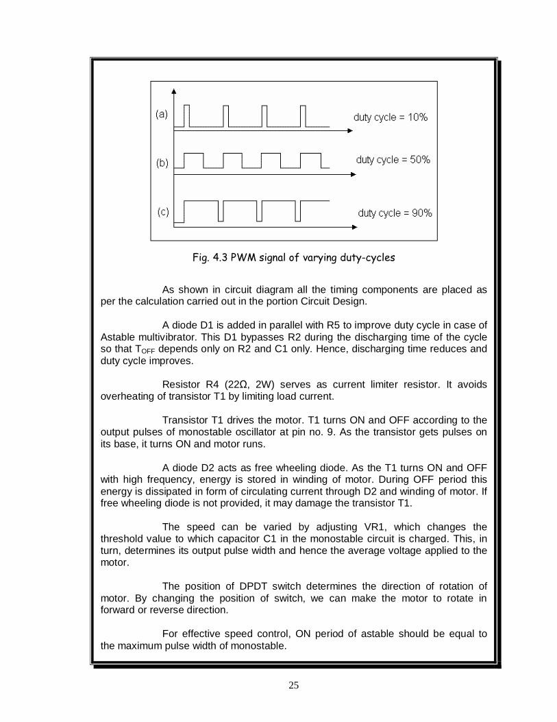
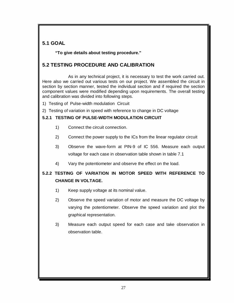