Embed Size (px)
Citation preview
SPECTRALLY PHASE CODED OPTICAL CODE DIVISION MULTIPLE ACCESS (O-CDMA) SYSTEM AND SPECTRAL LINE-BY-LINE PULSE SHAPING
A Thesis
Submitted to the Faculty
of
Purdue University
by
Zhi Jiang
In Partial Fulfillment of the
Requirements for the Degree
of
Doctor of Philosophy
May 2006
Purdue University
West Lafayette, Indiana

ii
This thesis is dedicated to my parents, Qifu Jiang and Youlan Tan.

iii
ACKNOWLEDGMENTS
I would like to thank Prof. Andrew M. Weiner for providing me the research opportunities, his superb guidance and consistent support in all aspects of my life at Purdue. Without his help, I would never imagine I can go this far. I would also like to thank my committee members, Prof. Jixin Cheng, Prof. James S. Lehnert, and Prof. Vladimir M. Shalaev, for taking time to consider my work.
Thank Dr. Daniel E. Leaird for making everything work and making the lab an enjoyable place to go. It would not have been such a productive time without his numerous technical support and invaluable help.
Thank the group members I am working with on the O-CDMA and line-by-line projects. Especially, thank Prof. Dongsun Seo for building the nice mode-locked laser and Dr. Shang-Da Yang for tutorial of PPLN device. Thank R. V. Roussev, C. Langrock, and Prof. M. M. Fejer at Stanford for providing the PPLN device. Thank all group members in our lab for their patience and friendship.
Thank all the friends for bringing fun and helping me out during hard times. Thanks are due to my previous advisors/mentors, Chongcheng Fan, Yousheng
Shu, Zhongying Miao and Weiguo Chen, for their encouragement over the years. Last but not least, my thanks go to my wife, Li Xu, for her love and support.

iv
TABLE OF CONTENTS Page LIST OF TABLES....................................................................................................... vii LIST OF FIGURES..................................................................................................... viii ABSTRACT................................................................................................................ xvii 1. INTRODUCTION������������������������.. 1 1.1 Optical Code Division Multiple Access (O-CDMA) System�����. 1 1.2 Spectral Line-by-Line Pulse Shaping��������������.. 5 2. MULTI-USER, ~Gb/s O-CDMA TESTBED........................................................ 12 2.1 Four User O-CDMA System Testbed �������������� 12 2.1.1 10 GHz 400 fs Pulse Source��������������. 13 2.1.2 Pulse Shaper Encoder/Decoder�������������. 13 2.1.3 Nonlinear Processing Based on PPLN����������.. 16 2.2 Four Users, 2.5 Gb/s System Experiments������������. 17 2.2.1 System Performance Measurement������������ 17 2.2.2 Multi-Level Codes and Capability of Programmable Coding�� 19 2.2.3 System Degradation Caused by Pulse Overlap Between Users�. 20 2.3 Four Users, 10 Gb/s System Experiments������������� 21 2.3.1 Slot-Level Timing Coordination Scheme Utilizing M-Sequence Coding.���������������������.. 21
2.3.2 Hybrid Chip and Slot-Level Timing Coordination Scheme Utilizing Double Hadamard Coding��������������. 23
3. RECONFIGURABLE ALL-OPTICAL CODE TRANSALTION IN SPECTRALLY
PHASE CODED O-CDMA NETWORKS��������������. 40 3.1 Introduction of Code Translation in O-CDMA Networks������� 40 3.2 Principle of Code Translation�����������������... 41 3.3 1-Stage Code Translation Experiment��������������.. 43 3.4 2-Stage Code Translation Experiment��������������. 45 3.5 Pulse Degradation Caused by Coding��������������.. 46
v
Page 3.6 Multi-Stage Code Translation�����������������. 49 3.6.1 Simulation of Multi-Stage Code Translation������...�� 49 3.6.2 Experimental Emulation of Multi-Stage Code Translation: Pulse Shaper in a Loop�������������������...�. 50 4. OPTICAL FIBER TRANSMISSION IN O-CDMA SYSTEM�����...�... 61 4.1 Pulse Distortion Caused by Fiber Dispersion����������...... 61 4.2 Fully Dispersion Compensated ~500 fs Pulse Transmission Over 50 km SMF ������������������������. 63 4.3 50 km SMF Fiber Transmission for O-CDMA.���������..� 65 5. SECURITY ISSUES IN O-CDMA SYSTEM ������������..� 71 5.1 Security Issues�����������������������. 71 5.2 Code Switching Scheme �������������������. 72 5.3 Vulnerability From Coding-Induced Spectral Dips���������. 74 5.4 Vulnerability From a DPSK Demodulator������������.. 76 6. SPECTRAL LINE-BY-LINE PULSE SHAPING������������. 85 6.1 Group Line Pulse Shaping Versus Line-by-Line Pulse Shaping���� 85 6.2 Spectral Line-by-Line Pulse Shaping �������������� 86 7. Width and Wavelength Tunable Optical RZ Pulse Generation and RZ-to-NRZ Format Conversion at 10 GHz Using Spectral Line-by-Line Control�����.. 92 7.1 Width and Wavelength Tunable Optical RZ Pulse Generation����.. 92 7.2 RZ-to-NRZ Format Conversion����������������.. 94 8. LINE-BY-LINE PULSE SHAPING CONTROL FOR OPTICAL ARBITRARY WAVEFORM GENERATION�����������������. 99 9. OPTICAL ARBITRARY WAVEFORM GENERATION AND
CHARACTERIZATION USING SPECTRAL LINE-BY-LINE CONTROL� 108 9.1 Experimental Setup���������������������.. 108 9.2 Results and Discussions�������������������... 110 10. LINE-BY-LINE PULSE SHAPING ON A PHASE MODULATED CW LASER 121 10.1 Experimental Setup��������������������� 122

vi
Page 10.2 Generation and Control of Spectral Lines������������. 123 10.3 CW-to-Pulse Conversion������������������... 124 10.4 Width and Wavelength Tunable RZ Pulse Generation������� 125 10.5 Single Line Filtering (Pulse-to-CW Conversion and Wavelength Conversion) ������������������������. 126 10.6 Correlation between Optical Spectra and Waveforms�������. 126 10.7 Correlation between Optical Spectra and RF Spectra�������.. 127 10.8 Microwave Waveform Synthesis��������������..� 129 10.9 Spectral Line Fluctuation and Its Impact on Line-by-Line Pulse Shaping 130 11. SUMMARY AND FUTURE RESEARCH DIRECTIONS�������.... 142 LIST OF REFERENCES................................................................................................. 145 VITA ........................................................................................................................... 155

vii
LIST OF TABLES Table Page 1.1 Comparison of O-CDMA schemes in terms of timing requirement (TR)�� 10 2.1 Reflective pulse shaper parameters.................................................................. 28 9.1 Line-by-line pulse shaper parameters����............................................... 73
viii
LIST OF FIGURES Figure Page 1.1 Schematic illustration of bandwidth allocation in TDM, WDM and CDMA optical networks. ...................................................................................................................... 9 1.2 Comparison of direct sequence RF-CDMA and spectral phase coded O-CDMA. (A) Time-domain behavior for RF-CDMA (equivalent to frequency-domain behavior for O-CDMA). (B) Frequency-domain behavior for RF-CDMA (equivalent to time-domain behavior for O-CDMA). .............................................................................................. 9 1.3 Timing control in O-CDMA optical networks................................................... 10 1.4 Conceptual diagram of an O-CDMA network. .................................................. 11 1.5 Illustration of different pulse shaping methodologies (a) Manipulating groups of lines. (b) Manipulating individual lines. ................................................................... 11 2.1 Four user O-CDMA system testbed................................................................... 26 2.2 10GHz 400fs pulse (A) intensity auto-correlation measurement and (B) optical spectrum..................................................................................................................... 26 2.3 Reflective pulse shaper used as encoder/decoder. f : focal length, PC: polarization controller, LCM: liquid crystal modulator. ................................................................ 27 2.4 Intensity cross-correlation measurements of uncoded (solid line) and 127 MS encoded (dotted line) pulses. Inset figure shows encoded pulse with enhanced vertical scale............................................................................................................................ 27 2.5 Intensity cross-correlation measurements. (A) uncoded (solid line) and 31 MS encoded (dotted line) pulses. (B) properly decoded (solid line) and improperly decoded (dotted line) pulses. .................................................................................................... 29 2.6 Optical spectra measurements. (A) uncoded, (B) 31 MS encoded, (C) properly decoded and improperly decoded. Optical spectrum analyzer (OSA) resolution: 0.05nm..................................................................................................................................... 29
ix
Figure Page 2.7 Periodically-poled lithium niobate (PPLN) waveguide second harmonic generation (SHG) phase matching spectrum. .............................................................................. 30 2.8 Intensity cross-correlation measurements of properly decoded channels 1 to 4 (A to D respectively) demonstrating the ability to selectively decode any of the four user channels. Channel 4 (D) is the uncoded user. ........................................................... 30 2.9 Eye diagrams prior to nonlinear processing (measurement point α in Fig. 3). Single user properly decoded (A), improperly decoded (B), two users (C), and four users (D). A & B demonstrate that both properly decoded and improperly decoded single user channels look essentially identical on a linear detector. C & D demonstrate that multiple users can not be adequately separated using linear detection. ................................................... 31 2.10 Eye-diagrams after nonlinear processing (measurement point β in Fig. 3), at -3dBm per user. (A) Properly decoded channel 1, single user. (B) Improperly decoded channel 1, single user. (C) Two users system, properly decode channel 1. D) Four users system, properly decode channel 2. A & B demonstrate the large contrast between a properly and improperly decoded single user channel. C & D demonstrate clear decoding of the desired user in a multiple user system via nonlinear processing. .............................. 31 2.11 Bit Error Rate (BER) measurements for single user (circles), 2 users (squares), 4 users (triangles). Decoded channel 1 and channel 2 and measured, respectively. Power refers to value at photoreceiver (�measurement point β�).......................................... 32 2.12 The same BER data as in Fig. 13, but replotted against the total power in the nonlinear discriminator (�measurement point α�). BER measurements for single user (circles), 2 users (squares), 4 users (triangles). Decoded channel 1 and channel 2 and measured, respectively.................................................... ........................................... 32 2.13 Length-31 binary (2-level) MS phase codes (A), quaternary (4-level) phase codes (B) and quadratic residues (31-level) phase codes (C)............................................ .. 33 2.14 Decoded channel 2 BER measurements with quaternary codes for single user (circles), 2 users (squares), 4 users (triangles). (A) power refers to value in nonlinear waveguide (�measurement point α�). (B) power refers to value at photoreceiver (�measurement point β�)......................................................... ................................... 33 2.15 Decoded channel 2 BER measurements with quadratic residue codes for single user (circles), 2 users (squares), 4 users (triangles). (A) power refers to value in nonlinear waveguide (�measurement point α�). (B) power refers to value at photoreceiver (�measurement point β�)............................................. ............................................... 34

x
Figure Page 2.16 Degradation caused by pulse overlapping between users. Eye diagrams for 2 users (channel 1 and 4) with separation (A) 0 ps (B) 10 ps (C) 20 ps (D) 30 ps separation with decoded channel 1................................................. ..................................................... 34 2.17 Illustration of system degradation caused by pulse overlap between users................................................. .......................................................................... 35 2.18 Intensity cross-correlation measurements of properly decoded user #1 to #4, demonstrating the ability to selectively decode any of the four users at 10 Gb/s... ... 35 2.19 Performance measurement of the 4x10 Gb/s O-CDMA system. (a) Eye diagram of properly decoded user #1 for 1 user, 2 users and 4 users. (b) BER measurements of user #1 corresponding to (a). (c) BER measurement of all 4 users. Powers refer to the values in the PPLN nonlinear discriminator... ...................................................................... 36 2.20 BER measurements and eye diagrams of properly decoded user #1 with one interference user while tuning the user separation. Performance is degraded when 2 users overlap........................................................................................................................ 37 2.21 (a) Spectrum before amplitude equalization. (b) Spectrum after amplitude equalization. (c) Double Hadamard code, consisting of 16 code elements on each half of the spectrum............................................................................................................... 38 2.22 Performance measurement of 10 Gb/s O-CDMA system with chip-level timing coordination. (a) Intensity cross-correlation of 1, 2 and 3 users with pulse user properly decoded. (b) Eye diagram and (c) BER measurement corresponding to (a). (d) BER measurement of one other properly decoded user...................................................... 38 2.23 Performance measurement of 4x10 Gb/s O-CDMA system with hybrid chip and slot-level timing coordination. (a) Intensity cross-correlation of 4 users with pulse user properly decoded. (b) Eye diagram and (c) BER measurement corresponding to (a). A: separate 4 users; B: overlap 3 MAI users, separate 1 desired user; C: separate 2 pairs of overlapping users; D: overlap 3 users including desired user, separate 1 MAI user 39 3.1 Conceptual diagram of all-optical code translation in an O-CDMA network. ... 53 3.2 Experimental apparatus for 1-stage code translation .......................................... 53 3.3 Intensity cross-correlation measurements of the desired user: (A) uncoded (B) encoded (C) translated and (D) properly decoded pulse ............................................ 54

xi
Figure Page 3.4 Intensity cross-correlation measurements of both desired and interference users .................................................................................................................................... 54 3.5 Eye diagrams and BER measurements of (A) single user without CT, (B) single user with CT, (C) 2 users without CT, and (D) 2 users with CT. CT: code translation ... 55 3.6 Experimental apparatus for 2-stage code translation .......................................... 55 3.7 (a) Intensity cross-correlation measurements of the desired user: (A) uncoded, (B) encoded, (C) translated once (D) translated twice, and (E) properly decoded pulses. (b) Length-31 quaternary phase codes applied to encoder, code translator 1, code translator 2, and decoder. ............................................................................................................... 56 3.8 BER measurements of 2-stage code translation for single user and 2 users. CT: code translation................................................................................................................... 56 3.9 Decoded pulse degradation caused by (A) 0 coding operations (uncoded pulse), (B) 2 coding operations, (C) 3 coding operations, and (D) 4 coding operations; (a) intensity cross-correlation measurements, (b) spectral measurements, (c) simulation of pulse intensities., and (d) simulation of spectra (uncoded spectrum is taken from experiment).................................................................................................................................... 57 3.10 Side-lobe of decoded pulses after 4 coding operations. (a) Intensity cross-correlation measurement. (b) Simulation of pulse intensity ..................................... 58 3.11 Comparison of experiment and simulation of pulse degradation caused by multiple coding operations (equivalently code-translation): normalized peak intensity (filled) and side-lobe energy (opened) .......................................................................................... 58 3.12 Pulse degradation caused by multi-stage code translation; (a) normalized peak intensity, and (b) normalized side-lobe energy. Two examples using different sets of quaternary codes are presented for 100 µm resolution .............................................. 59 3.13 Experimental apparatus for multi-stage code translation emulation: pulse shaper in a loop. PC: polarization controller. DC: dispersion compensating fiber. ................... 59 3.14 Intensity cross-correlation measurements of multi-stage code translation emulation. The numbers labeling the pulses represent the number of shaper passes. ................. 60 4.1 Experimental apparatus....................................................................................... 67

xii
Figure Page 4.2 Intensity cross-correlation with and without SMF/DCF module, demonstrating distortionless 50 km fiber transmission for sub-500 fs pulses................................... 67 4.3 Intensity cross-correlation for different pulse shaper settings. The inset figure shows an unwrapped version of the phase profile applied by the pulse shaper. The actual phase profile that is applied is modulo 2π........................................................................... 68 4.4 Intensity cross-correlation for different pulse shaper settings by inserting an additional 120 m SMF for complete second-order DC. The inset figure shows the unwrapped phase profile applied by the pulse shaper (again the actual phase is applied modulo 2π)................................................................................................................. 68 4.5 (A) Spectra before 50 km fiber link. (B) Spectra out of the 50 km fiber link showing spectral variation caused by PMD. Both (A) and (B) are measured through a polarizer; the three traces represent different polarization components. (C) Intensity auto-correlation for different polarization (PSP vs. non-PSP) at fiber link input. ............. 69 4.6 Intensity cross-correlation for a 2 user O-CDMA system after 50 km fiber transmission. .............................................................................................................. 70 4.7 BER performance for the O-CDMA system with and without 50 km fiber transmission. The inset figures show the eye diagrams for 2 users .......................... 70 5.1 Vulnerability illustration in the upstream traffic in a star network..................... 79 5.2 Experimental setup.............................................................................................. 79 5.3 Spectra and corresponding intensity cross-correlation of (a) uncoded , (b) coded arm 1 and (b) coded arm 2. (d) Waveform of the combined signals measured by photo-detector and sampling scope. ..................................................................................... 80 5.4 Spectra of (a) arm 1 without dip and (b) arm 2 with dip filtered by a narrow bandpass filter in the vicinity of 1542 nm. (c) Waveforms ....................................................... 80 5.5 Spectra and waveforms measurement. (a) Arm 1 with dip and arm 2 without dip. (b) Both with dip. (c) Both without dip ........................................................................... 81 5.6 Spectra and waveforms measurement using optical filters with different passband bandwidths for arm 1 without dip and arm 2 with dip............................................... 81 5.7 Spectra of (a) arm 1 and (b) arm 2 after post-processing. (c) Waveforms.......... 82

xiii
Figure Page 5.8 Spectra of (a) arm 1 and (b) arm 2 in the vicinity of 1542 nm after post-processing. (c) Waveforms ........................................................................................................... 82 5.9 Eye diagrams and BER measurements for authorized user: (a) single arm, (b) code-switching, (c) code-switching with post-processing .................................................. 83 5.10 Experimental setup to investigate vulnerability using a DPSK de-modulator. PC: polarization controller. PM: polarization maintaining.............................................. 84 5.11 (a) Waveforms after DPSK de-modulator. (b) Picking up several scans of the waveforms with clear eyes, to emphasize such possible vulnerabilities.................... 84 6.1 (A) Spectral lines without amplitude modulation. (B) Amplitude modulation by blocking every other line. (C) Two spectral lines. (D) Sampling scope traces with phase modulation (0, π/2, π and 3π/2) on one spectral line. The traces are the average of 100 measurements............................................................................................................. 90 6.2 (A) Two relatively stable spectral lines at 8.5 GHz. (B) Sampling scope traces with phase modulation (0 and π) on one spectral line. The traces are scanned 100 times. (C) Two relatively stable spectral lines at 10.5 GHz. (D) Sampling scope traces with phase modulation (0 and π) on one spectral line. The traces are scanned 100 times.......... 91 6.3 Another two examples for relatively unstable two lines..................................... 91 7.1 Line-by-line controlled spectra (linear scale) and waveforms, where the laser center wavelength is tuned to 1542 nm. The spectra are controlled to have (a) 2 lines, (b) 3 lines, (c) 4 lines and (d) 5 lines. These waveforms are detected by a 50 GHz photo-diode and sampling scope, showing tunable width of 50 ps, 33 ps, 25 ps and 20 ps, respectively. The spectra are controlled to have (e) 6 lines, (f) 10 lines, (g) 16 lines and (h) all lines. These waveforms are measured by intensity cross-correlation measurements, showing tunable width of 16 ps, 9 ps, 5 ps and 3 ps after de-convolution, respectively.......... 97 7.2 Line-by-line controlled spectra (linear scale) and waveforms, where 4 lines are transmitted through the line-by-line pulse shaper to generate 25 ps width pulses. Center wavelength is tuned to (a) 1532 nm and (b) 1562 nm by tuning both the mode-locked laser center wavelength and coarsely tuning the pulse shaper (the grating angle). Center wavelength is finely tuned around 1542 nm (c) and (d), by tuning pulse shaper alone (translation of slit)...................................................................................................... 98

xiv
Figure Page 7.3 RZ-to-NRZ format conversion by line-by-line pulse shaping. Spectra and eye-diagrams for (a) data modulated RZ format with 4 spectral lines, (b) converted NRZ format with only one spectral line. Inset figures show the spectra in log scale. (c) Bit-error-rate measurements for generated RZ format (solid square) and converted NRZ format (solid circle) by line-by-line pulse shaping; RZ format (open square) and converted NRZ format (open circle) after 25 km single mode fiber transmission without dispersion compensation............................................................................................ 98 8.1 Experimental apparatus for arbitrary waveform generation using line-by-line pulse shaper. The inset figure shows a measured 3 dB passband of 2.6 GHz. LCM: liquid crystal modulator. PC: polarization controller. ....................................................... 104 8.2 Selecting two spectral lines (separated by A: 10 GHz, B: 20 GHz, C: 100 GHz, E: 400 GHz and F: 500 GHz) and corresponding cosine waveforms (with periods of 100 ps, 50 ps, 10 ps, 2.5 ps and 2 ps). The inset spectra figures in Fig. (A-C) are in linear scale to show the well-controlled relative amplitudes of the two selected lines and the strong suppression of the deselected lines. Fig. (D) shows the simulation results for a distorted cosine waveform with 18 dB suppression ratio of adjacent lines due to limited pulse shaper resolution ...................................................................................................... 105 8.3 Selecting four spectral lines, in which two lines in each pair are separated by 10 GHz and the two inner lines between the two pairs are separated by 400 GHz. The center to center separation of the line pairs is 410 GHz. The resulting waveforms have 100 ps macro period (corresponding to 10 GHz) and 2.44 ps micro period (corresponding to 410 GHz). The red and blue waveforms are controlled to be out of phase by applying π phase shift on one pair of spectral lines, as shown in the zoomed figures......................... 106 8.4 Selecting four spectral lines (five consecutive lines with center line blocked). (B,C) Waveforms measured by intensity cross-correlation with different applied spectral phases (red and blue curves). Calculations (black circles) are essentially indistinguishable from the data, showing the high fidelity of the generated waveforms. (D,E) Waveforms are detected by a 50 GHz photo-diode and measured by sampling scope in persistent mode to demonstrate radio frequency arbitrary waveform generation (RF-AWG) ............... 107 9.1 Experimental setup for O-AWG and its characterization using spectral line-by-line control ...................................................................................................................... 116 9.2 (a) Two spectral lines selected. (b) Sampling scope traces with phase modulation (0, π/2, π and 3π/2) on one spectral line. The traces are the average of 20 measurements .................................................................................................................................. 117
xv
Figure Page 9.3 Five spectral lines with one line missing generated by spectral line-by-line pulse shaping. (a) Spectral intensity measured with an OSA in linear and log scale (inset). (b) Measured spectral phase using spectral line-by-line control ................................... 118 9.4 Two selected spectral lines and corresponding delayed cosine waveforms measured by a sampling scope ................................................................................................. 118 9.5 Waveform temporal intensity (a) and temporal phase (b) corresponding to Fig. 5. Solid lines: Fourier Transform of measured spectral intensity and phase. Dashed lines: Fourier Transform with nominal spectral phase applied by the LCM. Circles: intensity measured by the sampling scope (only in (a)). Diamonds: intensity measured by intensity cross-correlation (only in (a)). All the waveforms in (a) are normalized to unity for comparison............................................................................................................... 119 9.6 Thirteen spectral lines with cubic spectral phase generated by spectral line-by-line pulse shaping. (a) Spectral intensity measured with an OSA in linear and log scale (inset). (b) Measured spectral phase using spectral line-by-line control. Inset shows unwrapped spectral phase with cubic characteristics............................................... 119 9.7 Comparison between measured spectral phases of 13 lines and the nominal phases corresponding to the 15 pixels of the LCM. The measured spectral phases are adjusted by adding a constant and linear phase onto the unwrapped spectral phases in the inset of Fig. 8(b). The pixel positions are mapped onto the wavelength accordingly................. 120 9.8 Waveform temporal intensity (a) and temporal phase (b) corresponding to Fig. 8. Solid lines: Fourier Transform of measured spectral intensity and phase. Diamonds: intensity measured by intensity cross-correlation (only in (a)) ................................ 120 10.1 Experimental setup.......................................................................................... 132 10.2 Line-by-line pulse shaper. The inset figure shows a measured 3 dB passband of 2.6 GHz. LCM: liquid crystal modulator. PC: polarization controller ........................ 132 10.3 Spectra of (a) input CW (b) phase modulated CW at 9.0 GHz (c) phase modulated CW at 9.0 GHz but tuning the input CW wavelength (d) phase modulated CW at 13.5 GHz. ......................................................................................................................... 133 10.4 CW-to-pulse conversion. (a) Sampling scope trace of phase modulated CW. (b) Pulses measured via sampling scope after spectral phase correction (circles) and calculation (solid line). (c) Measured (squares) and calculated (solid line) pulse intensity auto-correlation ........................................................................................................ 134

xvi
Figure Page 10.5 Width and wavelength tunable return-to-zero pulse generation. The spectra are controlled to have (a) two lines, (b) three lines and (c) four lines. The corresponding waveforms have width of 55 ps, 37 ps and 28 ps. These pulses also have different and adjustable center wavelengths.................................................................................. 135 10.6 Pulse-to-CW conversion and CW-to-CW wavelength conversion. (a) Optical spectrum of one filtered line, which is different from the input CW wavelength. (b) Corresponding CW waveform detected by a photo-diode and (c) RF spectrum ..... 136 10.7 Effects of suppression ratio on the waveforms. Circles in the waveforms are measured data while the lines are calculated ideal cosine waveforms. Spectra in (a)~(c) are log scale and spectra in (d)~(f) are linear scale.................................................. 137 10.8 Correlation between optical spectra and waveforms for two spectral lines.... 138 10.9 Correlation between optical spectra and RF spectra for three spectral lines. (a) Three lines with identical phases. (b) Three lines with one line π phase shift.................. 138 10.10 Correlation between optical spectra and RF spectra for three spectral lines with identical phases, where the two outside lines are controlled to have equal intensity. (a) Center line higher than outside lines. (b) Center line lower than outside lines. (c) RF spectra contrast ratio versus optical spectra contrast ratio ....................................... 139 10.11 Two selected spectral lines are controlled to be separated by (a) 1×9 GHz, (b) 2×9 GHz, (c) 3×9 GHz, (d) 4×9 GHz, (e) 5×9 GHz, (f) 6×9 GHz and (g) 7×9 GHz. The corresponding microwave signals are generated after O/E conversion using a 50 GHz photo-diode. RF spectra are measured for (a)~(e) to show the harmonics suppression .................................................................................................................................. 140 10.12 Two selected spectral lines are separated by (a) 10 GHz and (b) 13.5 GHz by changing the RF driving frequencies accordingly.................................................... 141 10.13 (a) Unstable spectral lines and corresponding waveforms from actively mode-locked fiber laser running at 10.5 GHz. Noise process is observed when applying π phase shift on one of the two lines. (b) Stable spectral lines and corresponding waveforms from a modulated CW at 10.5 GHz. No such noise process is observed ........................ 141
xvii
ABSTRACT Jiang, Zhi Ph.D., Purdue University, May 2006. Spectrally Phase Coded Optical Code Division Multiple Access (O-CDMA) System and Spectral Line-by-Line Pulse Shaping. Major Professor: Andrew M. Weiner.
Multiple access techniques are required to meet the demand for high-speed and large-capacity communications in optical networks, which allow multiple users to share the fiber bandwidth. Optical code-division multiple-access (O-CDMA) is receiving increased attention due to its potential applications for local area optical networks. We experimentally investigate an ultrashort pulse O-CDMA scheme based on spectral phase encoding and decoding of coherent mode-locked laser pulses. Strong interference suppression is achieved by using a novel, ultrasensitive nonlinear optical intensity discriminator based on second harmonic generation (SHG) in a periodically-poled lithium niobate (PPLN) waveguide. We have experimentally demonstrated/investigated: (1) 4-user, 2.5 Gb/s and 10 Gb/s O-CDMA system with ultra-low power (~30 fJ/bit); (2) reconfigurable all-optical code translation in our O-CDMA testbed; (3) 50 km single mode fiber (SMF) transmission experiments for O-CDMA system; (4) security issues in O-CDMA networks.
We have built the first grating-based spectral line-by-line pulse shaper and
demonstrated many functionalities: (1) demonstrated line-by-line pulse shaping experiments in which the individual spectral lines present in the output of a mode-locked laser with ~10 GHz mode spacing are resolved. The shaped pulses overlap in time, which leads to a new way to observe fluctuations of the comb-offset frequency in the time domain; (2) demonstrated line-by-line pulse shaping control for optical arbitrary waveform generation (O-AWG); (3) demonstrated tunable return-to-zero signal generation, return-to-zero to non-return-to-zero format conversion; (4) demonstrated complete intensity and phase measurement of optical pulses using spectral line-by-line pulse shaping; (5) in addition to utilizing the spectral lines generated from a mode-locked

xviii
laser, we also applied line-by-line pulse shaping control on spectral lines generated from a phase modulated continuous wave (CW) laser. Based on these apparatus, we showed various optical processing functionalities, including CW-to-pulse conversion, width and wavelength tunable return-to-zero pulse generation, pulse-to-CW conversion, wavelength conversion and microwave waveform synthesis.

1
1. INTRODUCTION
There are two major parts in this work: (1) spectrally phase coded optical code
division multiple access (O-CDMA) system; (2) spectral line-by-line pulse shaping. Although these two are relatively independent work, they share one thing common: pulse shaper is the most critical component for both of them.
1.1 Optical Code Division Multiple Access (O-CDMA) System Multiple access techniques are required to meet the demand for high-speed and
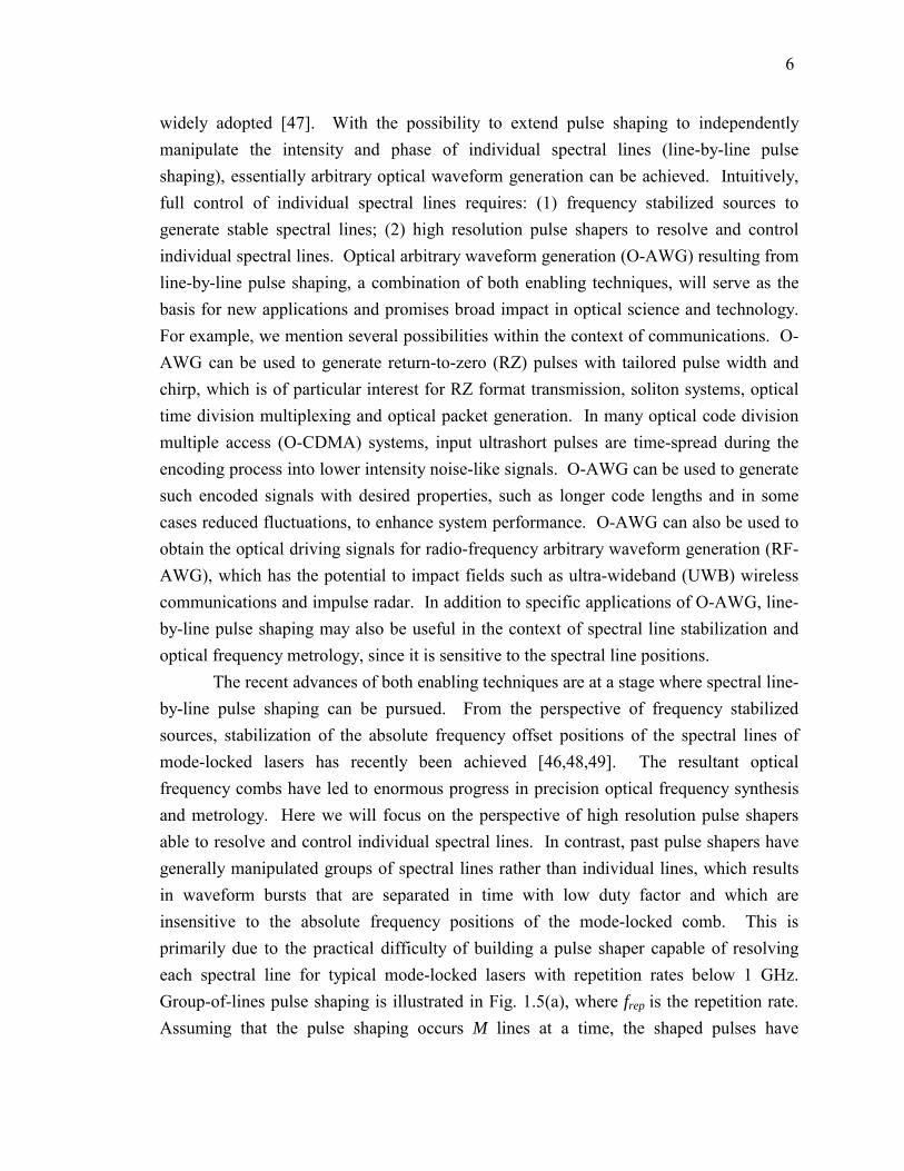
large-capacity communications in optical networks, which allow multiple users to share the fiber bandwidth. There are three major multiple access approaches: each user is allocated a specific time slot in time-division multiplexing (TDM), and a specific frequency (wavelength) slot in wavelength division multiplexing (WDM). Both techniques have been extensively explored and utilized in optical communication systems [1-6]. Alternatively, optical code-division multiple-access (O-CDMA) [7-34] is receiving increasing attention due to its potential for enhanced information security, simplified and decentralized network control, improved spectral efficiency, and increased flexibility in the granularity of bandwidth that can be provisioned. In O-CDMA, different users whose signals may be overlapped both in time and frequency share a common communications medium; multiple-access is achieved by assigning different, minimally interfering code sequences to different CDMA transmitters, which must subsequently be detected in the presence of multi-access interference (MAI) from other users. Fig. 1.1 shows a schematic illustration of bandwidth allocation in TDM, WDM and O-CDMA.
CDMA derives from radio frequency (RF) spread spectrum communications, originally developed for military applications due to an inherent low probability of intercept and immunity to interference, and more recently for commercial RF cellular radio applications [35,36]. CDMA is now becoming the dominant multiple access technique in RF wireless networks. Since RF-CDMA works with typical carrier frequencies in the ~1 GHz range and bit rates on the order of ~100kb/s, current electronic technologies can easily provide coding and long temporal code (~1000 chips) for each bit,
2
which is critical to support a large number of potential users [7]. In addition, the bit error rate (BER) requirement is usually not so strict for RF-CDMA. In contrast, the need to perform encoding and decoding for O-CDMA poses one immediate challenge both because of the optical carrier frequency and the much higher bit rate of ~Gb/s per user, which already approaches the limit of electronic processing. Therefore, innovative all-optical processing technologies are needed. In addition, the challenges for O-CDMA also come from critical requirements which are routinely required in optical communication systems. These requirements include: extreme high quality of service (QoS) (BER at 10-9 or below), large capacity (tens or hundreds of users, total capacity up to ~100 Gb/s or above), and long distance (kilometers to ~100 km for local area networks (LAN) and metropolitan area networks (MAN)).
Several different O-CDMA schemes have been proposed [8-34], based on different choices of sources, coding schemes and detection. Significant progresses of O-CDMA research have been achieved worldwide in recent years [37-45]. O-CDMA schemes may be classified according to the choice of coherent versus incoherent processing, coherent (mode-locked pulses) versus incoherent (e.g., amplified spontaneous emission (ASE) and light emitting diode (LED)) broadband optical source, and encoding method (time-domain versus frequency-domain, amplitude versus phase). Schemes based on incoherent processing (summing of optical powers) and broadband incoherent (noise) sources are generally the easiest to implement but offer relatively poor performance. To increase the available coding space, time-wavelength (2-Dimension) coding schemes have been proposed, where each code chip corresponds to a specific time position and wavelength position within a bit as determined by a code matrix [22,30,31]. This scheme may utilize either coherent or incoherent sources but employs incoherent processing (summing of optical powers from chips with different wavelength and time positions). However, as in radio spread spectrum systems, coherent processing based on manipulation of optical fields, which can be made to sum to zero, is needed for strongest suppression of MAI and for best performance. Here, we experimentally investigate an ultrashort pulse O-CDMA scheme based on spectral phase encoding and decoding of coherent modelocked pulses [10,15]. A theoretical analysis of the MAI limited performance of this approach indicates the potential for O-CDMA systems with capacities from tens to perhaps ~100 Gb/s in fully asynchronous operation, depending on how short a pulse width and how long a code length can be implemented in the system [10].

3
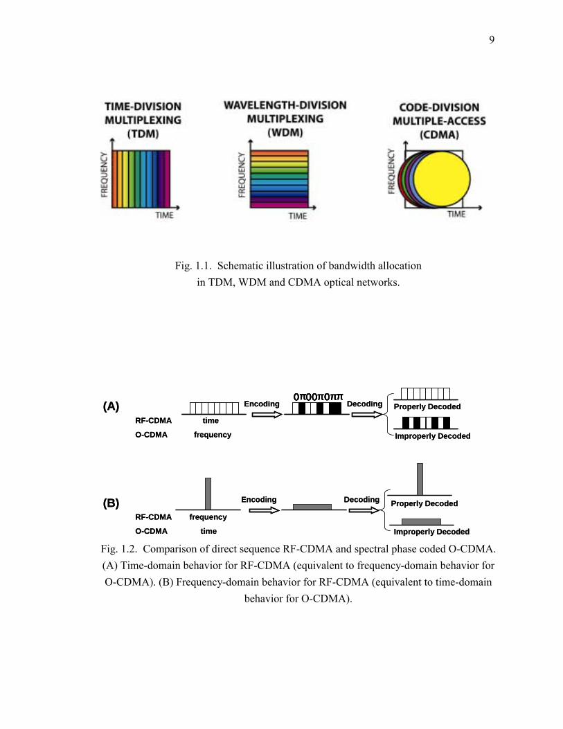
Our ultrashort pulse O-CDMA scheme based on spectral phase encoding has an interesting analogy with the most widely used direct sequence (DS) RF-CDMA. Fig. 1.2 shows time and frequency domain evolution during encoding-decoding for these two schemes. For DS RF-CDMA, a bit is divided into many temporal chips and phase coded for each chip (for example, 0 or π phase shift for bipolar phase shift keying (BPSK)) in the time domain (Fig. 1.2(A)), so that the spectrum of a narrow band signal is broadened during the encoding process (Fig. 1.2(B)). After decoding at the receiver, a properly decoded signal is recovered back to a narrow band signal, which can be separated out by a narrow band filter from the improperly decoded broadband MAI. This encoding-decoding process manifests the spread spectrum property of DS RF-CDMA [35,36] where there exists a trade-off between bandwidth and performance. Our O-CDMA scheme is just a time-frequency reversed version of DS RF-CDMA, where the ultrashort pulse spectrum is divided to many frequency chips and phase coded for each chip (Fig. 1.2(A)). This results in spreading in the time domain (Fig. 1.2(B)), while proper decoding despreads the encoded signal back to its original duration in time.
CDMA is well suited for bursty network environments, and the asynchronous nature of data transmission can simplify and decentralize network management and control. However, due to system requirements mentioned above, full asynchronism is difficult to implement in practice while simultaneously maintaining sufficient MAI suppression. Therefore, some level of synchronism is built into many ≥ 2-user O-CDMA schemes. The time scales relevant for a discussion of synchronism requirements are illustrated in Fig. 1.3. The coarsest time scale is the bit period, tbit. Uncoded or properly decoded waveforms have a duration which is called the chip duration, tchip. Encoded or improperly decoded pulses are pseudonoise waveforms with a larger duration, which we refer to as the slot duration tslot. In our spectral phase coded O-CDMA scheme, the individual features in the pseudonoise waveforms have characteristic durations equal to tchip, and the number of independent features is equal to the code length N, i.e., tslot / tchip = N. For a fully asynchronous system signals transmitted by any user can fall anywhere within a bit duration tbit without coordination with other users. In a fully synchronous system, the signal transmitted by any specific user must be coordinated with the transmission time of all the other users, with a timing precision below tchip. Furthermore, a synchronous receiver would require optical clock recovery for gating with timing precision also below tchip. To relax the timing requirements of the fully synchronous approach, we propose here the concept of slot level coordination � the transmission time of a user is controlled on the time scale of the slot duration tslot, but without the need for

4
chip level timing control. Accordingly, O-CDMA can be classified according to different levels of synchronism requirements. At the transmitter side, we distinguish no coordination (full asynchronism) vs. slot level (tslot) coordination vs. chip level (tchip) coordination. At the receiver side, we distinguish asynchronous detection vs. synchronous detection requiring chip level (tchip) speed (either electronically or via optical gating with clock recovery). All the possible combinations are listed in Table 1.1 with representative references. It is clear that chip level transmission coordination and/or synchronous detection requiring chip level (tchip) speed are used in many ≥ 2-user O-CDMA schemes. This sacrifices one of the most significant advantages, asynchronism, of CDMA. In contrast, our scheme only requires slot level coordination, and fully asynchronous detection is achieved by means of a novel, asynchronous nonlinear optical processing technique. We also investigate chip level timing coordination in our system, which shows potential to increase user numbers.
Fig. 1.4 shows the conceptual O-CDMA network diagram for many of the O-CDMA approaches. Input ultrashort pulses are time-spread during the encoding process into lower intensity noise-like signals [15-34]. In the receiver, data corresponding to a desired user is separated from MAI via a matched filtering (decoding) operation, in which properly decoded signals are converted back to the original pulse-like signals, while improperly decoded signals remain low-intensity noise-like temporally broad waveforms. Since the energy in properly and improperly decoded signals remains similar, and since the temporal duration of even improperly decoded signals is on the order of the bit period or below, both properly and improperly decoded signals will appear essentially identical to an electronic receiver band-limited to the data rate. Consequently either very fast electronics or a nonlinear optical intensity discriminator play a critical role in separating properly decoded short pulses from improperly decoded MAI. In our testbed, successful information recovery from MAI is achieved by the use of a novel, ultrasensitive nonlinear optical intensity discriminator based on second harmonic generation (SHG) in a PPLN waveguide.
The progress we have achieved are summarized as follows: • In our work, we demonstrate a 4-user spectral phase coded O-CDMA system
operating at 2.5 Gb/s and 10 Gb/s with strong nonlinear interference suppression. Compared to previous work, the key points are the following: (1) full interference suppression with 4 users at Gb/s rates without the need for chip level timing coordination or synchronous gating; (2) the use of a novel, ultrasensitive nonlinear optical intensity discriminator based on second harmonic generation (SHG) in a
5
periodically-poled lithium niobate (PPLN) waveguide. Our nonlinear discriminator permits full MAI suppression at an operating energy of ~30 fJ/bit, as much as two orders of magnitude lower than previous discriminators based on nonlinear fiber optics [15,16,20,21,25,33]. The ability to operate at low power per user is critical for scaling an O-CDMA system to multiple users. In multi-user networking each receiver will see a sample of each of the multiple-access signals; therefore, the required amplifier saturation power scales with the number of users (as well as bit rate) [2,3].
• Based on our O-CDMA system testbed, we are able to experimentally investigate various O-CDMA research issues. We have experimentally demonstrated reconfigurable all-optical code translation in our O-CDMA testbed for both 1-stage and 2-stage code translations. Multi-stage code translations are investigated via simulation and experimental emulation in a loop pulse shaper to show the potential application of our method for up to several tens of code translations.
• We have demonstrated essentially distortionless 50 km fiber transmission for ~500 fs pulses using dispersion compensating fiber and a programmable pulse shaper as a spectral phase equalizer. Based on this technique, we have also demonstrated the successful operation of our ultrashort pulse O-CDMA system at the same distance.
• We have experimentally investigated the security issues in O-CDMA system. Among other possible advantages provided by O-CDMA, its potential for enhanced information security is frequently mentioned. However, we experimentally demonstrated possible vulnerabilities even without knowledge of the codes. Our work shows that there may be many opportunities for exploiting structure in coded OCDMA signals for eavesdropping, even without learning the code.
1.2 Spectral Line-by-Line Pulse Shaping
Mode-locked lasers generate periodic trains of ultrashort pulses which are characterized in the frequency domain by an evenly spaced series of discrete spectral lines (an optical frequency comb), with the frequency spacing equal to the pulse repetition rate [46]. Spectral lines and their stabilization in mode-locked lasers have recently played a critical role in the progress of optical frequency metrology and optical carrier-envelope phase control [46]. Meanwhile, pulse shaping techniques, in which intensity and phase manipulation of optical spectral components allow synthesis of user-specified ultrashort pulse fields according to a Fourier transform relationship, have been developed and
6
widely adopted [47]. With the possibility to extend pulse shaping to independently manipulate the intensity and phase of individual spectral lines (line-by-line pulse shaping), essentially arbitrary optical waveform generation can be achieved. Intuitively, full control of individual spectral lines requires: (1) frequency stabilized sources to generate stable spectral lines; (2) high resolution pulse shapers to resolve and control individual spectral lines. Optical arbitrary waveform generation (O-AWG) resulting from line-by-line pulse shaping, a combination of both enabling techniques, will serve as the basis for new applications and promises broad impact in optical science and technology. For example, we mention several possibilities within the context of communications. O-AWG can be used to generate return-to-zero (RZ) pulses with tailored pulse width and chirp, which is of particular interest for RZ format transmission, soliton systems, optical time division multiplexing and optical packet generation. In many optical code division multiple access (O-CDMA) systems, input ultrashort pulses are time-spread during the encoding process into lower intensity noise-like signals. O-AWG can be used to generate such encoded signals with desired properties, such as longer code lengths and in some cases reduced fluctuations, to enhance system performance. O-AWG can also be used to obtain the optical driving signals for radio-frequency arbitrary waveform generation (RF-AWG), which has the potential to impact fields such as ultra-wideband (UWB) wireless communications and impulse radar. In addition to specific applications of O-AWG, line-by-line pulse shaping may also be useful in the context of spectral line stabilization and optical frequency metrology, since it is sensitive to the spectral line positions. The recent advances of both enabling techniques are at a stage where spectral line-by-line pulse shaping can be pursued. From the perspective of frequency stabilized sources, stabilization of the absolute frequency offset positions of the spectral lines of mode-locked lasers has recently been achieved [46,48,49]. The resultant optical frequency combs have led to enormous progress in precision optical frequency synthesis and metrology. Here we will focus on the perspective of high resolution pulse shapers able to resolve and control individual spectral lines. In contrast, past pulse shapers have generally manipulated groups of spectral lines rather than individual lines, which results in waveform bursts that are separated in time with low duty factor and which are insensitive to the absolute frequency positions of the mode-locked comb. This is primarily due to the practical difficulty of building a pulse shaper capable of resolving each spectral line for typical mode-locked lasers with repetition rates below 1 GHz. Group-of-lines pulse shaping is illustrated in Fig. 1.5(a), where frep is the repetition rate. Assuming that the pulse shaping occurs M lines at a time, the shaped pulses have

7
maximum duration ~1/(Mfrep) and repeat with period T=1/frep. Accordingly, the pulses are isolated in time. In contrast, for line-by-line pulse shaping (M=1) as shown in Fig. 1.5(b), the shaped pulses can overlap with each other, which leads to waveforms spanning the full time period between mode-locked pulses (100% duty factor). Waveform contributions arising from adjacent mode-locked pulses will overlap and interfere coherently in a manner sensitive to the offset of the frequency comb [50]. Such line-by-line control makes true O-AWG possible since the intensity and phase of each individual spectral line is fully controlled. Group-of-lines pulse shaping can be considered as a special case of line-by-line pulse shaping. All group-of-lines pulse shaping results can be achieved using a line-by-line pulse shaper, by simply applying identical intensity/phase on each group of lines. Previous efforts towards spectral line-by-line control utilized a hyperfine filter but were limited within a narrow optical bandwidth - the free spectral range of this device [51, 52].
We have demonstrated spectral intensity/phase line-by-line pulse shaping and thus O-AWG over a considerably broader band based on high resolution grating-based pulse shapers. The progress we have achieved are summarized as follows: • We have demonstrated line-by-line pulse shaping experiments in which the
individual spectral lines present in the output of a mode-locked laser with ~10 GHz mode spacing are resolved. The shaped pulses overlap in time, which leads to a new way to observe fluctuations of the comb-offset frequency in the time domain.
• We have demonstrated line-by-line pulse shaping control for optical arbitrary waveform generation (O-AWG) and radio frequency arbitrary waveform generation (RF-AWG). Independent manipulation of the spectral amplitude and phase of individual lines over a broad optical band from a mode-locked frequency comb leads to synthesis of user-specified ultrafast optical waveforms with unprecedented control.
• Based on spectral line-by-line control, we have demonstrated tunable return-to-zero signal generation and return-to-zero to non-return-to-zero format conversion.
• Complete intensity and phase measurement of optical pulses using spectral line-by-line pulse shaping. By manipulating individual spectral lines, the spectral phase relationship between adjacent spectral lines can be extracted from the time-domain measurements.
• In addition to utilizing the spectral lines generated from mode-locked laser, we also applied line-by-line pulse shaping control on spectral lines generated from a phase modulated continuous wave (CW) laser. Based on this apparatus, we showed

8
various optical processing functionalities, including CW-to-pulse conversion, width and wavelength tunable return-to-zero pulse generation, pulse-to-CW conversion, wavelength conversion and microwave waveform synthesis.
9
Fig. 1.1. Schematic illustration of bandwidth allocation in TDM, WDM and CDMA optical networks.
RF-CDMA frequency
O-CDMA time
Encoding Decoding
Encoding Decoding Properly Decoded
Improperly Decoded
Properly Decoded
Improperly Decoded
0000ππππ00000000ππππ0000ππππππππ
RF-CDMA time
O-CDMA frequency
(A)
(B)RF-CDMA frequency
O-CDMA time
Encoding Decoding
Encoding Decoding Properly Decoded
Improperly Decoded
Properly Decoded
Improperly Decoded
0000ππππ00000000ππππ0000ππππππππ
RF-CDMA time
O-CDMA frequency
(A)
(B)
Fig. 1.2. Comparison of direct sequence RF-CDMA and spectral phase coded O-CDMA. (A) Time-domain behavior for RF-CDMA (equivalent to frequency-domain behavior for O-CDMA). (B) Frequency-domain behavior for RF-CDMA (equivalent to time-domain
behavior for O-CDMA).

10
tchiptbit
ttslottchiptbit
ttslot
Fig. 1.3. Timing control in O-CDMA optical networks.
Table 1.1. Comparison of O-CDMA schemes in terms of timing requirement (TR).
No coordination
Slot level coordination
Chip level coordination
Asynchronous detection (via nonlinear optical processing)
TR: low Ref: [16,44,45]
TR: medium Ref: this work
TR: high Ref: [33]
Synchronous detection requiring chip level (tchip) speed (either electronically or via optical gating with clock recovery)
TR: high Ref: [22,27]
TR: high Ref: -
TR: high Ref: [19,20,21,32, 37,38,39, 40,41,43]
TR: timing requirement, Ref: references Note: Not all the references include a sufficiently detailed timing discussion. For references [19], [22], [27], detection was clearly based on gating with chip-level synchronism; however, the level of timing coordination at the transmitter was not clearly specified. In those cases we made the classification according to our best interpretation.
Receiver requirement
Transmitter requirement

11
Receiver
Other users Other users
Transmitter
Encoder Decoder andNonlinear O/E
Receiver
Other users Other users
Transmitter
Encoder Decoder andNonlinear O/E
Fig. 1.4. Conceptual diagram of an O-CDMA network.
Shaping: group of lines Shaping: individual linesFrequency domain frep
frequency
frep
Time domain
time1/frep 1/frep
Repetition period (1/frep)
time1/frep 1/frep
Overlapped regime
(b)(a)
Μ frep
1/(Μ frep)
frequency
Shaping: group of lines Shaping: individual linesFrequency domain frep
frequency
frep
Time domain
time1/frep 1/frep
Repetition period (1/frep)
time1/frep 1/frep
Overlapped regime
(b)(a)
Μ frep
1/(Μ frep)
frequency
Fig. 1.5. Illustration of different pulse shaping methodologies (a) Manipulating groups of
lines. (b) Manipulating individual lines.
12
2. MULTI-USER, ~Gb/s O-CDMA TESTBED
In this chapter, we describe the ultrashort pulse spectral phase coded O-CDMA testbed and key enabling components in section 2.1. Four-user 2.5 Gb/s and 10 Gb/s system experimental results are presented in section 2.2 and 2.3, respectively. The results in this chapter have been published in [53-55]. 2.1 Four User O-CDMA System Testbed
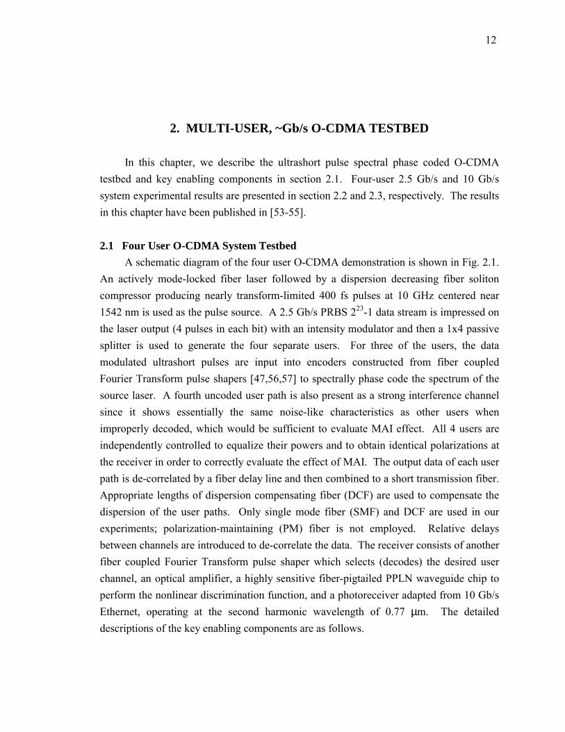
A schematic diagram of the four user O-CDMA demonstration is shown in Fig. 2.1. An actively mode-locked fiber laser followed by a dispersion decreasing fiber soliton compressor producing nearly transform-limited 400 fs pulses at 10 GHz centered near 1542 nm is used as the pulse source. A 2.5 Gb/s PRBS 223-1 data stream is impressed on the laser output (4 pulses in each bit) with an intensity modulator and then a 1x4 passive splitter is used to generate the four separate users. For three of the users, the data modulated ultrashort pulses are input into encoders constructed from fiber coupled Fourier Transform pulse shapers [47,56,57] to spectrally phase code the spectrum of the source laser. A fourth uncoded user path is also present as a strong interference channel since it shows essentially the same noise-like characteristics as other users when improperly decoded, which would be sufficient to evaluate MAI effect. All 4 users are independently controlled to equalize their powers and to obtain identical polarizations at the receiver in order to correctly evaluate the effect of MAI. The output data of each user path is de-correlated by a fiber delay line and then combined to a short transmission fiber. Appropriate lengths of dispersion compensating fiber (DCF) are used to compensate the dispersion of the user paths. Only single mode fiber (SMF) and DCF are used in our experiments; polarization-maintaining (PM) fiber is not employed. Relative delays between channels are introduced to de-correlate the data. The receiver consists of another fiber coupled Fourier Transform pulse shaper which selects (decodes) the desired user channel, an optical amplifier, a highly sensitive fiber-pigtailed PPLN waveguide chip to perform the nonlinear discrimination function, and a photoreceiver adapted from 10 Gb/s Ethernet, operating at the second harmonic wavelength of 0.77 µm. The detailed descriptions of the key enabling components are as follows.

13
2.1.1 10 GHz 400 fs Pulse Source A home-made actively mode-locked fiber laser [58] is used which allows center
wavelength tuning from 1535 to 1560 nm and repetition rate tuning from 8 GHz to 13 GHz, while keeping a 2.5~3.5 ps (FWHM) short pulse. In the current work the center wavelength is 1542 nm and repetition sequence is 9.9988 GHz generating a 2.6 ps pulse. In order to achieve sufficient bandwidth for O-CDMA spectral phase coding, the laser output is followed by a dispersion decreasing fiber (DDF) soliton compressor to produce nearly transform-limited ~400 fs pulses assuming hyperbolic secant pulse shape. An intensity auto-correlation measurement of the pulses after the DDF and the optical spectrum are shown in Fig. 2.2. 2.1.2 Pulse Shaper Encoder/Decoder
Both encoding and decoding are implemented by the well developed ultrashort pulse shaping techniques using a fiber coupled Fourier-Transform pulse shaper which incorporates a 128 element liquid crystal modulator (LCM) array to spectrally phase code the spectrum of the source laser. The individual pixels of the LCM can be electronically controlled independently to give an arbitrary phase shift in the range of 0 to 2π with twelve bit resolution. Fig. 2.3 shows the reflective pulse shaper configuration used in our experiment [59]. Since the diffraction grating in our setup is polarization dependent, a polarization controller (PC) is used before circulator port 1. A collimator is connected to circulator port 2. A telescope could be inserted after the collimator to magnify the beam size on the grating in order to enhance the spectral resolution. Discrete frequency components making up the input short pulse are horizontally diffracted by the grating and focused by the lens at the retro-reflecting mirror. The LCM is placed just before the lens focal plane to enable programmable spectral phase coding. A retro-reflecting mirror leads to a double pass geometry, with all the frequencies recombined into a single fiber and with the output from circulator port 3. The pulse shaper is easily programmed under computer control, which allows convenient testing of various code families.
In order to optimize system performance, we investigated several pulse shaper designs for use in O-CDMA. In general, high spectral resolution and low loss are the most critical issues in the designs. Unfortunately, there exists a trade off between high resolution and low loss in our current designs. More code chips for spectral phase coding can be achieved in a high resolution pulse shaper, which is critical to scale to large number of users in O-CDMA implementations [10]. The resolution here is defined as the beam diameter (intensity decreases to 1/e2 of peak value) at the LCM plane for each

14
single frequency component. Since 128 pixels of the LCM cover 12.8 mm, each with ~100 µm active width, a maximum of 128 coded chips is feasible if the resolution is equal to or less than 100 µm. Fig. 2.4 shows intensity cross-correlation measurements of uncoded and encoded pulses with such a high-resolution shaper. The uncoded (LCM set for all pixels at zero phase) pulse is quite similar to the input 400 fs pulse which is characteristic of a well aligned pulse shaper. The encoded pulse is broadened to an ~100 ps pseudonoise waveform by spectral phase coding with a length-127 M-sequence (MS) code (a pseudorandom binary phase code with phase shifts of 0 or π) [35]. 127 pixels are used for the length-127 code, while setting the unused pixel at 0 phase. The 15.6 dB peak intensity contrast ratio between the two traces clearly illustrates the stretching of input short pulses into time-spread noise-like pulses by pseudo-random spectral phase coding. The inset figure shows an encoded pulse with enhanced vertical scale to demonstrate the fine temporal structure present on the encoded waveform. The 8.5 dB fiber-to-fiber insertion loss of this high resolution shaper is relatively high due to poor coupling back to the large beam size (5.4mm) collimator, which has to be used to achieve small beam size (high resolution) at the LCM layer. Loss reduction is possible by optimizing the fiber to free-space beam delivery system.
Constructing a low loss pulse shaper is important for practical application in the O-CDMA system. Using a smaller beam size (1.9mm) collimator, we are able to achieve as low as 4.0 dB fiber-to-fiber insertion loss, which is the lowest value ever reported. The loss is distributed as follows: 2.0 dB from the polarization controller and circulator, 1.0 dB from the LCM, and the remaining 1.0 dB from other components including collimator input/output coupling, grating diffraction loss, lens and retro-reflective mirror. Alignment related loss is included in this latter 1.0 dB. Further loss reduction perhaps may require lower loss components (e.g., the circulator). The resolution at the LCM plane is degraded to 300 µm due to the smaller beam size collimator, which supports up to 42 spectral chips because each chip has to be represented by 3 pixels. Nevertheless, it is sufficient for our system experiment where length-31 codes are used.
In order to form a matched encoder-decoder pair, the spectral coding range covered by the 128 pixels of the LCM has to be identical for both shapers. In addition, due to its programmable nature, the decoder in our experiments can be tuned to decode each of the 4 users. Consequently, all four pulse shapers (3 encoders and 1 decoder) are carefully constructed to have a nearly identical spectral phase coding range. The detailed parameters of these four pulse shapers and the high resolution pulse shaper discussed above are listed in Table 2.1. Note that the matched encoder-decoder pair does not
15
necessarily require identical pulse shaper designs, but only requires identical spectral coding range and sufficient resolution. Actually, the designs of the four pulse shapers implemented in our system experiment are considerably different, including diverse selections of collimators, gratings and lenses. This demonstrates, for the first time to our knowledge, successful implementation of an encoder-decoder pair using different pulse shaper designs. These pulse shapers are used for 4 user, 2.5 Gb/s system experiment. In our later experiments, all pulse shapers are upgraded to have the same parameters as decoder.
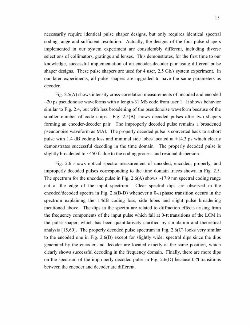
Fig. 2.5(A) shows intensity cross-correlation measurements of uncoded and encoded ~20 ps pseudonoise waveforms with a length-31 MS code from user 1. It shows behavior similar to Fig. 2.4, but with less broadening of the pseudonoise waveform because of the smaller number of code chips. Fig. 2.5(B) shows decoded pulses after two shapers forming an encoder-decoder pair. The improperly decoded pulse remains a broadened pseudonoise waveform as MAI. The properly decoded pulse is converted back to a short pulse with 1.4 dB coding loss and minimal side lobes located at ±14.3 ps which clearly demonstrates successful decoding in the time domain. The properly decoded pulse is slightly broadened to ~450 fs due to the coding process and residual dispersion.
Fig. 2.6 shows optical spectra measurement of uncoded, encoded, properly, and improperly decoded pulses corresponding to the time domain traces shown in Fig. 2.5. The spectrum for the uncoded pulse in Fig. 2.6(A) shows ~17.9 nm spectral coding range cut at the edge of the input spectrum. Clear spectral dips are observed in the encoded/decoded spectra in Fig. 2.6(B-D) whenever a 0-π phase transition occurs in the spectrum explaining the 1.4dB coding loss, side lobes and slight pulse broadening mentioned above. The dips in the spectra are related to diffraction effects arising from the frequency components of the input pulse which fall at 0-π transitions of the LCM in the pulse shaper, which has been quantitatively clarified by simulation and theoretical analysis [15,60]. The properly decoded pulse spectrum in Fig. 2.6(C) looks very similar to the encoded one in Fig. 2.6(B) except for slightly wider spectral dips since the dips generated by the encoder and decoder are located exactly at the same position, which clearly shows successful decoding in the frequency domain. Finally, there are more dips on the spectrum of the improperly decoded pulse in Fig. 2.6(D) because 0-π transitions between the encoder and decoder are different.

16
2.1.3 Nonlinear Processing Based on PPLN As discussed in the introduction section, a nonlinear optical intensity discriminator
plays a critical role in separating properly decoded short pulses from improperly decoded MAI. In our testbed, successful information recovery from MAI is achieved by the use of a novel, ultrasensitive nonlinear optical intensity discriminator based on second harmonic generation (SHG) in a PPLN waveguide. The PPLN chip is 67 mm long with 62 mm periodically poled and a channel waveguide fabricated by reverse proton exchange [61]. The propagation losses were 0.2 dB/cm. Fig. 2.7 shows the PPLN waveguide SHG phase matching spectrum, which exhibits a sinc2-shape with 0.17 nm bandwidth centered at 1542 nm by temperature tuning to 92.5 oC. Its center wavelength shifts ~0.1nm/Co, with almost the same profile. The phase matching bandwidth is consistent with 18.6 ps temporal walk-off between the fundamental and SHG fields. Asymmetry of the phase matching curve may be attributed to uneven temperature distribution across the PPLN chip. The measured internal SHG efficiency at the peak of the phase matching curve is 3100%/W for continuous wave (CW) and 170%/pJ for ultrashort pulses. In the future even higher efficiency and thus stronger discrimination may be possible by fabricating even longer waveguides.
The use of a waveguide structure together with a long nonlinear medium leads to dramatically increased SHG conversion efficiency for uncoded or properly decoded (bandwidth-limited) pulses [61]; on the other hand, SHG can be strongly suppressed for spectral phase encoded or improperly decoded pulses. Roughly speaking, two distinct mechanisms can contribute to suppression of the SHG signal. First, in conventional SHG with large phase matching bandwidth, the SHG efficiency scales inversely with the pulse width. Second, in SHG with large group velocity walk-off, where the device phase matching bandwidth is much narrower than the input spectrum (as in our experiments), phase modulation on the pulse can also strongly suppress the conversion efficiency. More precisely, one can control the SHG yield by changing the correlation properties of the applied spectral phase code sequences [62,63]. In this way, the ability to discriminate between uncoded (properly decoded) and encoded (improperly decoded) pulses is greatly enhanced. As a result, second harmonic power contrast ratios of up to 20.1 dB between uncoded and encoded waveforms were observed when coding with a length-31 MS code in experiments at 10 GHz, with less than 1 mW average power (100 fJ per pulse) in the PPLN waveguide [64]. A key point is that the pulse energies required here are approaching two orders of magnitude lower than those required in previous O-CDMA

17
decoding experiments based on nonlinear fiber optics. Later we will show that our system can be operated as low as ~30 fJ per bit for 4 user, 10 Gb/s system. 2.2 Four Users, 2.5 Gb/s System Experiments
In this section we present the system experiments, which combine all the key components to form an O-CDMA testbed as shown in Fig. 2.1.
2.2.1 System Performance Measurement
Fig. 2.8 demonstrates the ability to properly decode any of the four user channels by the correct selection of decoder spectral phase code � here a length 31 MS code. The figure shows intensity cross correlation measurements of the non-data-modulated stream measured at �measurement point α� (just before the nonlinear processor) shown in Fig. 2.1. In our experiment, the pulses from each user are roughly separated by ~25 ps for a time-slotted O-CDMA scheme. There is no need for precise control of the time offsets. Fig. 2.8 clearly demonstrates that the properly decoded user is converted back to a short pulse, while the improperly decoded users (MAI) are noise-like temporally broadened waveforms. These noise-like waveforms show distinct fine temporal structure due to the superposition of different spectral phase codes in the encoder and decoder. For example, user 1 and user 2 will see different noise-like waveforms from interference user 3.
The need for a nonlinear pulse discriminator is dramatically illustrated in Fig. 2.9, where we use a conventional 1.5 µm photo-detector optimized for the 2.5 Gb/s data rate to detect the decoder output prior to entering the nonlinear processor. Fig. 2.9 shows the temporal profile of both properly decoded (A - short pulse) and improperly decoded (B - temporally broadened) signals, as seen on a sampling scope. Other than the very small amplitude difference due to coding loss in the pulse shaper, there is no noticeable difference between the signals. This clearly illustrates the main issue in O-CDMA with ultrashort pulses: properly decoded and improperly decoded waveforms have fundamentally the same energy, which means they produce the same output from a relatively slow electronic detector, even though they can show strong differences in temporal structure and peak intensity on an ultrafast time scale (as shown in Fig. 2.8). Further, in a system environment, the signals from all users will be superimposed when viewed by a conventional photoreceiver with bandwidth optimized for the data rate. Fig. 2.9(C) and (D) show cases of 2 and 4 users; the eyes are completely closed. It is very interesting to observe the double and quadruple eyes in (C) and (D). For the 2 user case in (C), the double eye can be understood by the following. The top line of the eye
18
corresponds to �1� bits that are transmitted by both users because the power is doubled. The bottom line of the eye corresponds to �0� bits that are transmitted by both users because the power is blocked by intensity modulation of the data stream. The middle line of the eye corresponds to �1� and �0� bits that are transmitted by either of the 2 users while the second user transmits the conjugate state. In addition, since the probability of transmitting a �1� bit or �0� bit by each of the 2 users is twice that of simultaneously transmitting either �1� bit or �0� bit, there are twice the number of points in the middle line of the eye, resulting in darker middle lines shown in the figure. A similar explanation follows for the (barely visible) quadruple eyes of 4 users in Fig. 2.9(D). From another perspective, these figures also confirm that all 4 users are fully de-correlated by the different fiber delays experienced by each channel. It is also interesting to point out that for a single user, a relatively slow linear electronic detector can be used to correctly detect the signal even if the spectral phase code is unknown because both properly and improperly decoded pulses show essentially the same output as shown in Fig. 2.9(A) and (B). This means that the potential security advantage of O-CDMA is not realized in a single user system employing on-off keying. However, security can still exist as shown in Fig. 2.9(C) and (D) in a multi-user environment, which is of practical interest.
Nonlinear processing enables us to separate these temporally overlapped signals thereby permitting a multi-user system. Fig. 2.10 (A) to (D) respectively show the output of the receiver (measurement point β in Fig. 5), for a single properly decoded user, a single improperly decoded user, two users (channel 1 properly decoded), and four users (channel 2 properly decoded) at a power in the nonlinear processing element of -3 dBm per user. The clean eye diagrams clearly demonstrate the ability to properly decode the desired channel, and separate it from the interference channels.
Fig. 2.11 shows Bit Error Rate (BER) curves for 1, 2, and 4 users at 2.5 Gb/s plotted vs. the power at the photoreceiver (�measurement point β�), with either channel 1 or 2 decoded. In all cases we were able to measure BERs down to less than 10-11. There is a power penalty of roughly 1.5 dB per interfering user (similar for both decoded channels), which we attribute at least in part to the finite interference suppression ratio of the nonlinear discriminator.
Fig. 2.12 shows the same BER data as in Fig. 2.11, but replotted against the total power in the nonlinear discriminator (�measurement point α�). With perfect interference suppression, the power required at the discriminator should scale proportional to the number of users. The data show almost exactly 3 dB power increase in going from 1 to 2

19
users, just as expected. An additional ~4.5 dB is required in going from 2 to 4 users (for 10-11 BER). This is ~1.5 dB above the 3 dB expected value, which means there is an ~1.5 dB power penalty referenced to the input of the nonlinear discriminator. The key point, however, is that we are able to run the four-user experiment at only ~0.65 mW per user in the nonlinear element, which provides substantial margin for scaling to higher bit rates and user counts while provisioning only a moderately sized optical amplifier to each receiver node. More precisely, for a single user the required power in the nonlinear element at 10-11 BER is ~-3.7 dBm, which corresponds to an average energy of 171 fJ/bit at 2.5 Gb/s. For 4 users the required power (~4 dBm) corresponds to an average energy of 251 fJ/bit per user.
To understand the importance of O-CDMA system operating at low power levels, the power scaling issue is briefly discussed as follows. For proper operation the self-gated nonlinear discriminator key to our scheme requires some value Ubit to achieve certain BER performance, where Ubit is the energy required per bit for a single properly decoded user. Since equal samples of each channel are seen by every O-CDMA receiver, the average power required at the nonlinear element is 0.5CBUbit, where C is the number of channels, B is the data rate, and the factor 0.5 comes from on-off keying. Previous demonstrations of O-CDMA nonlinear discriminators were based on nonlinear fiber optics, where typical values for Ubit range from 5-50 pJ [15,25]. For four 2.5 Gb/s channels, this gives an average power requirement of 14-24 dBm at each receiver. Scaling to significantly higher bit rates and channel numbers would require a very large optical amplifier at each receiver, which is highly undesirable for application to networks with large numbers of nodes. To address this scaling issue, it is critical to reduce Ubit. Our experiments using waveguide SHG generation achieve ~200 fJ/bit at 2.5Gb/s, a reduction approaching two orders of magnitude compared to discriminators based on nonlinear fiber optics. 2.2.2 Multi-Level Codes and Capability of Programmable Coding
Our programmable pulse shaping technique provides flexibility and ease of use in switching to different spectral codes. This could be very helpful in a network environment since code sequence selection plays a critical role in determining the performance of CDMA communication systems [65]. As an example of this capability, in addition to binary MS codes demonstrated in previous sections, we have also applied a 4-level (quaternary) family A code [65] and a 31-level quadratic residue code [66], as

20
shown in Fig. 2.13 together with a binary MS code for comparison. Based on the coding literature, multi-level code families can provide a larger number of distinct code sequences with small cross-correlation [65]. Fig. 2.14 and Fig. 2.15 shows BER measurements for decoded channel 2, which are obtained by encoding and decoding all users with length-31 quaternary codes and quadratic residue codes, respectively. Note that the aggregate powers before nonlinear O/E differ less than 3 dB between 2 users and 1 user, most possibly because the improperly decoded user experiences higher coding loss than properly decoded user as illustrated by more spectral dips shown in Fig. 2.6, which seems to have a bigger effect on multi-level coding. For 4 users, the quaternary code shows slightly improved performance to the MS codes while the quadratic residue code suffers slight degradation. To our knowledge, this is the first demonstration of greater than 4-level phase coding in O-CDMA systems. 2.2.3 System Degradation Caused by Pulse Overlap Between Users
In our 4 user O-CDMA demonstration, based on nonlinear processing, there is no need for precise (chip level) coordination of transmission times or for clock recovery and synchronous gating in the receiver, as discussed in the introduction. However, we have introduced a slot level coordination scheme and intentionally separated the 4 users in the time domain, as shown in Fig. 2.8. We have found that system performance is significantly degraded as pulses overlap between users. Fig. 2.16 shows the eye diagrams for a 2 user experiment while tuning the pulse separation. When the pulses from the 2 users are overlapped completely (0 ps separation), the properly decoded user is seriously degraded by the interference channel. The eye becomes clear with increasing temporal separation. The degradation caused by overlapping is almost negligible when the separation is larger than ~20 ps. Obviously, such degradation is a kind of beat noise between the signal and interference.
As a qualitative explanation consider the following example. If the number of chips in the code is N = 100, the broadened interference waveform intensity is approximately 1% of the short pulse signal peak intensity. When there is no temporal overlap, the impact of interference is very small after nonlinear processing, since the nonlinear discriminator strongly suppresses the interference signal and any remaining interference that leaks through the discriminator simply adds (in power) to the desired signal. However, when temporal overlap occurs, the optical fields (not power) sum at the input of the nonlinear device. For the prior example, the interference field amplitude is 10% of the signal field amplitude during the interval of the short pulse. Therefore, the beat noise

21
intensity fluctuation could be as large as ±20% (worst case) of the signal intensity (illustrated in Fig. 2.17). The size of the fluctuation, which is already large, may be increased by the nonlinear optical processing � whether this is performed using an SHG device as here, using fiber based nonlinear optical devices [15,33], or using other nonlinear devices. The effect of beat noise in ultrashort pulse O-CDMA has been fully analyzed when an ideal thresholder is used at the receiver [10]. But further analysis is needed when practical, asynchronous nonlinear optical processing devices are placed before the O/E conversion, which of course will depend strongly on the detailed mechanism of the particular nonlinear optical processing device. Degradation caused by overlap is a universal problem for multi-user O-CDMA systems [20,21,27,32,33]. Proposed remedies include optical gating [20,21,27] and/or chip level timing coordination [32,33]. Optical gating requires clock recovery and a synchronous reference pulse train at the receiver, while chip level timing coordination requires synchronous control at the transmitter. As a result both methods sacrifice the advantage of asynchronism. Further investigation into interference suppression methods is needed. 2.3 Four Users, 10 Gb/s System Experiments
In this section, we discuss two implementations of a 4-user, 10 Gb/s spectrally phase coded O-CDMA system: (1) slot-level timing coordination scheme using M-sequence coding, which is similar to previous 2.5 Gb/s system; (2) hybrid chip and slot-level timing coordination scheme using double Hadamard coding. In our terminology the chip time is the duration of uncoded or properly decoded short pulses, typically ~1 ps or below. The slot duration is a much longer time scale equal to or longer than the encoded or improperly decoded pseudonoise waveforms, corresponding to relaxed timing control. 2.3.1 Slot-Level Timing Coordination Scheme Utilizing M-Sequence Coding
The system testbed is similar to 4 users, 2.5 Gb/s as shown in Fig. 2.1, except that now a 10 Gb/s PRBS 223-1 data stream is impressed on the ~0.4 ps, 10 GHz mode-locked fiber laser output. Fig. 2.18 demonstrates the ability to properly decode any of the four user channels by the correct selection of decoder spectral phase code � here a length-31 M-sequence code. Again, the pulses from each user are roughly separated by ~25 ps in a time-slotted O-CDMA scheme. There is no need for precise chip-level control of the time offsets. Fig. 2.19(a) shows the eye diagrams of properly decoded user #1 for 1 user, 2 users and 4 users respectively. The clean eye diagrams clearly demonstrate the ability to properly decode the desired user, and separate it from the MAI. Fig. 2.19(b) shows

22
corresponding bit error rate (BER) curves for user #1 plotted vs. the total power in the nonlinear discriminator. The ~3 dB power differences between BER curves are simply due to the doubling of the number of users. This implies almost negligible power penalty induced by MAI. The key point is that we can operate with 1 user at BER=10-9 at a power level of less than -5.5 dBm (28.2 fJ/bit), and 4 users at less than 1 dBm (31.5 fJ/bit), showing significant improvement compared with other approaches utilizing optical fiber nonlinearities. Fig. 2.19(c) shows BER curves for all 4 users. Even the worst channel, in which we attribute the degradation to the finite interference suppression of the nonlinear discriminator, still operates at BER=10-9 with a four-user power of 2 dBm (39.6 fJ/bit). From a system point of view, it is important to run all 4 users successfully since MAI may exhibit distinct suppression characteristics for each specific desired user. In our system, the ~30 fJ/bit requirement provides substantial margin for scaling to higher bit rates and user counts while provisioning only a moderately sized optical amplifier to each receiver node.
Although both the current 10 Gb/s and the previous 2.5 Gb/s experiments utilized the same 10 GHz mode-locked laser source and 10 Gb/s Ethernet receiver, the current 10 Gb/s experiments require ten times lower energy per bit and lower overall power in the nonlinear discriminator. We attribute this substantial improvement to several sources. First, in the current 10 Gb/s experiment, all the energy per bit is in a single pulse, which is more efficient in driving the nonlinear discriminator than a 2.5 Gb/s data stream with 4 pulses per bit and correspondingly reduced peak power. Second, a lower modulation rate data stream adapted from a higher repetition pulse laser source [32,33] introduces additional power penalty in the system. Third, there is ~2 dB receiver sensitivity improvement for RZ vs. NRZ signaling [67]. Finally, we put significant effort in optimizing system performance, including encoder/decoder pair matching, PPLN waveguide phase matching temperature tuning, dispersion compensation, etc. The overall result of all these factors is to yield the ~10dB improvement in the energy requirement per user while increasing the data rate by 4 times.
We emphasize that our scheme only requires slot level timing coordination, and nonlinear processing and detection is fully asynchronous. In the experiments we intentionally separated the 4 users in the time domain (Fig. 2.18). We have observed in 2.5Gb/s experiment that the system performance is degraded as pulses overlap between users. Here we quantify the degradation in 10 Gb/s system by BER measurement. Fig. 2.20 shows the eye diagrams and corresponding BER measurement for a 2-user experiment while tuning the separation between the users. Length-31 M-sequence coding
23
is still used such that the interference user is broadened to an ~20 ps pseudonoise waveform. Negligible degradation is observed when the 2 users separation is >15 ps. At 12.5 ps separation the BER can still be pushed down to 10-10, which shows the possibility to run 8 slotted 10 Gb/s users distributed in the 100 ps bit duration. When the user separation is <10 ps, performance is seriously degraded and depends on the precise relative timing and phase of the overlapping users. In general, performance is better when the desired user (properly decoded short pulse) is located at a dip rather than at a spike of the interference waveform. This explains why BER performance at 7.5 ps separation is slightly better than that at 8.5 ps separation. Finally, BER is degraded to 10-
4~10-3 within a 5 ps separation range. 2.3.2 Hybrid Chip and Slot-Level Timing Coordination Scheme Utilizing Double Hadamard Coding
In our slot-level timing coordination scheme using M-sequence coding, system performance is degraded as pulses overlap between users (equivalently, time slot duration is decreased). This is due to beat noise caused by the interaction between the desired user and MAI, which is a universal problem for multi-user O-CDMA systems. To suppress MAI effectively, many O-CDMA systems have relied on precise timing coordination at the transmitter and/or synchronous nonlinear gating at the receiver, with coordination/synchronism required at the level of the finest feature in the coded waveforms - equal to the duration of uncoded or properly decoded pulses, typically on the order of a picosecond or below [20,21,27,32,33]. This is referred to as chip-level timing coordination, which requires much more stringent timing control than slot-level timing coordination since the slot duration is much longer than the chip duration. In general, increasing timing coordination and synchronism can provide greater user counts and better performance, at the cost of greater complexity. In this section, we discuss the O-CDMA system performance with increased timing control at the transmitter but still without synchronous detection at the receiver.
Considering the narrow band SHG process due to large group velocity mismatch in PPLN waveguide, one can control the SHG yield by changing the correlation properties of the applied spectral phase code; our group has previously demonstrated as much as 30 dB MAI suppression ratio using a double Hadamard code, showing potential for O-CDMA application [62,63]. Here we propose a modified double Hadamard coding scheme: at the transmitter each user is coded by a double Hadamard code (H1:H2, H1≠H2) across the whole spectrum, and at the receiver it is properly decoded back to a short pulse

24
by the same code (H1:H2) or improperly decoded by another code (H3:H4). Double Hadamard coding requires spectral amplitude equalization, for which the SHG at the center wavelength becomes equal to the spectral correlation [62]. As a result, proper sets of double Hadamard codes are fully orthogonal and ideally give zero crosstalk between orthogonal codes and consequently full MAI suppression. This property remains valid in a chip-level timing coordination scheme even when pulses overlap between users.
Our experimental setup is the same as Fig. 2.1, except the 2x128 pixel liquid crystal modulator (LCM) arrays in pulse shaper now spectrally phase code and amplitude equalize the spectrum of the source laser. Compared to the previous 10 Gb/s experiment, three important changes are: (1) spectral amplitude equalization, (2) chip-level timing control is introduced, and (3) the double-Hadamard coding scheme. Fig. 2.21(a) shows the optical spectrum before amplitude equalization. Fig. 2.21(b) shows the equalized spectrum without spectral phase coding, for which the 9 nm bandwidth covers 64 pixels of the LCM. Fig. 2.21(c) shows one typical double Hadamard code. We use a length-16 Hadamard code (16 code elements) on each half of the spectrum with 2 pixels per code-element. Note that the code-element order is reversed on each half of the spectrum.
Before discussing hybrid chip and slot-level timing coordination, we investigate the system performance of chip-level timing coordination. Fig. 2.22 shows the O-CDMA system results with chip-level timing coordination. All users are aligned at the chip-level time scale with ~ps accuracy. Fig. 2.22(a) shows intensity cross correlation measurements in which the pulse user is properly decoded, for 1 user, 2 users and 3 users respectively. Approximately a 5-ps wide minimum occurs at the center of the interference user waveforms where the properly decoded short pulse is located, enhancing the MAI rejection. Double length-16 Hadamard coding is used resulting in an interference user waveform broadened to ~25 ps. Fig. 2.22(b) and (c) shows corresponding eye diagrams and bit error rate (BER) curves as a function of power at the nonlinear discriminator. To increase from 1 user to 2 users, the ~3.5 dB power differences between BER curves at BER=10-9 implies 0.5 dB power penalty due to MAI, since 3 dB arises from doubling of the number of users. Similarly, with 3 users a total of ~1.2 dB power penalty caused by MAI is observed at BER=10-9. Fig. 2.22(d) shows the BER curves for another properly decoded user. There is ~2.7 dB power difference compared with the pulse user shown in (c), mostly caused by coding degradation and coding loss. This is larger than our previous results due to the higher resolution used in our current pulse shapers. Nevertheless, BER curves (c) and (d) show essentially similar behavior except for the power difference.
25
Fig. 2.23 shows the 4-user O-CDMA system results with hybrid chip and slot-level timing coordination with the pulse user properly decoded. Fig. 2.23(a) shows intensity cross correlation measurements of 4 combinations: A) 4 users separated in a time-slotted configuration; B) overlap 3 MAI users, separate 1 desired user; C) separate 2 pairs of overlapping users; D) overlap 3 users including the desired user, separate 1 MAI user. Fig. 2.23(b) and (c) shows corresponding eye diagrams and BER curves, all operating at less than 3 dBm for 4 users (~50 fJ/bit) at BER=10-9.
Considering the ~25 ps slot occupied by each user, there are 4 available slots for the 100 ps bit duration at 10 Gb/s. This implies the potential of a 12-user O-CDMA system if there are 3 users with chip-level timing coordination within each of the 4 slots. In our system, the low power requirement provides substantial margin for scaling to higher bit rates and user counts while provisioning only a moderately sized optical amplifier to each receiver node, operating at practical power levels compatible with traditional optical communication systems. Although chip and slot-level timing coordination is required in this scheme, fully asynchronous detection is achieved through the asynchronous nonlinear optical processing technique. We briefly compare 4-user, 10 Gb/s O-CDMA system implementations in section 2.3.1 and 2.3.2: (1) slot-level timing coordination scheme utilizing M-sequence coding, which requires relatively simple control; (2) hybrid chip and slot-level timing coordination scheme utilizing double Hadamard coding, which has potential to support greater user counts at the cost of greater complexity.
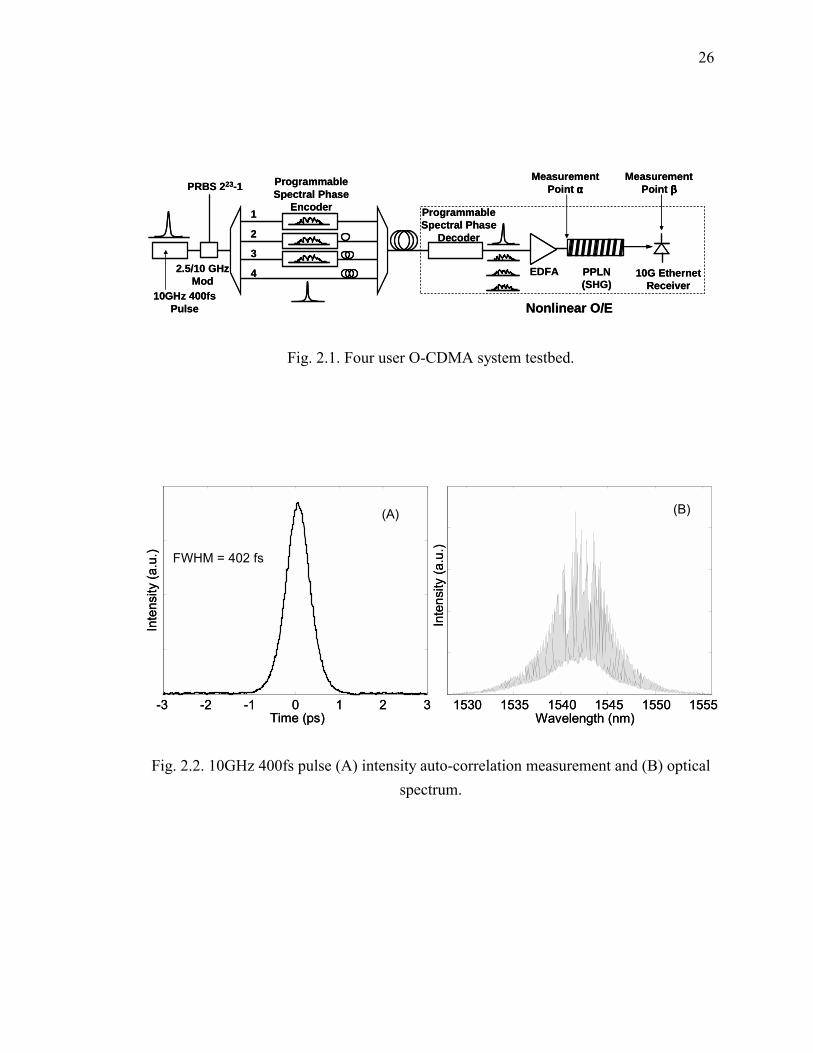
26
10G Ethernet Receiver
PPLN (SHG)
10GHz 400fs Pulse
Programmable Spectral Phase
Encoder Programmable Spectral Phase
Decoder
EDFA2.5/10 GHzMod
PRBS 223-1
Nonlinear O/E
MeasurementPoint αααα
MeasurementPoint ββββ
1
2
3
4 10G Ethernet Receiver
PPLN (SHG)
10GHz 400fs Pulse
Programmable Spectral Phase
Encoder Programmable Spectral Phase
Decoder
EDFA2.5/10 GHzMod
PRBS 223-1
Nonlinear O/E
MeasurementPoint αααα
MeasurementPoint ββββ
1
2
3
4
Fig. 2.1. Four user O-CDMA system testbed.
1530 1535 1540 1545 1550 1555Wavelength (nm)
Inte
nsity
(a.u
.)
(B)
-3 -2 -1 0 1 2 3Time (ps)
Inte
nsity
(a.u
.) FWHM = 402 fs
(A)
1530 1535 1540 1545 1550 1555Wavelength (nm)
Inte
nsity
(a.u
.)
(B)
-3 -2 -1 0 1 2 3Time (ps)
Inte
nsity
(a.u
.) FWHM = 402 fs
(A)
Fig. 2.2. 10GHz 400fs pulse (A) intensity auto-correlation measurement and (B) optical spectrum.
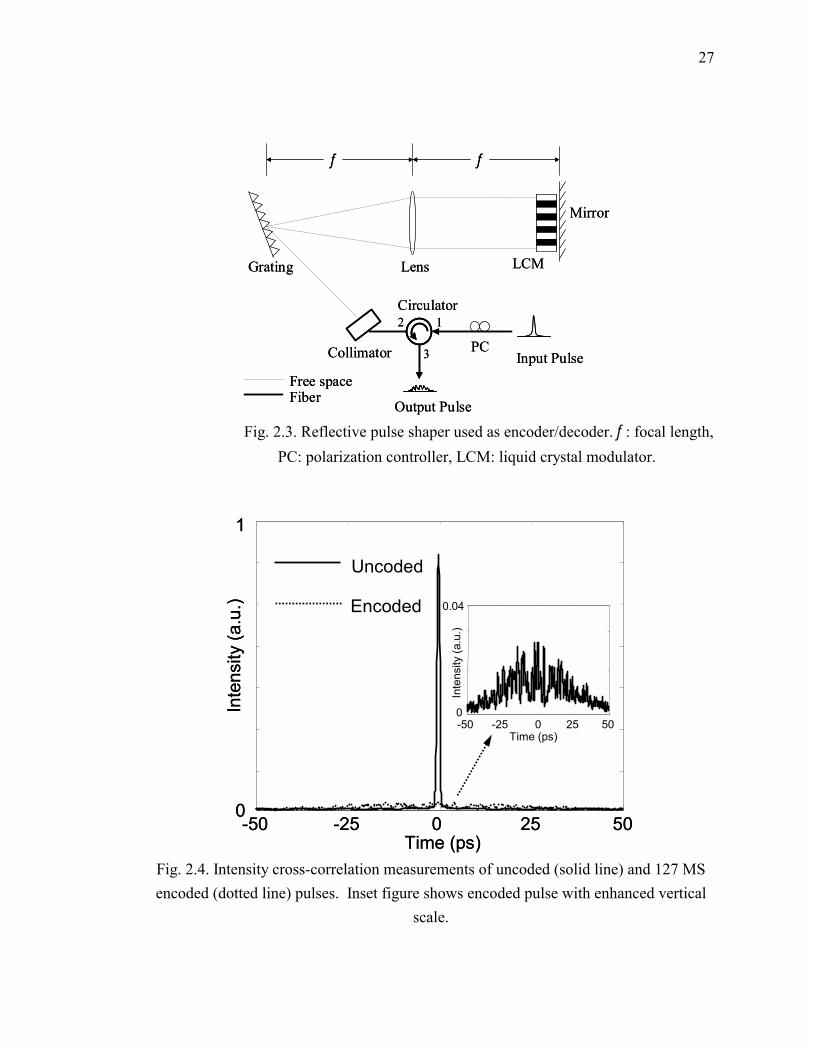
27
Grating LCMLens
PC
Mirror
Circulator
Input PulseCollimator
f f
Output Pulse
Free spaceFiber
1
3
2
Grating LCMLens
PC
Mirror
Circulator
Input PulseCollimator
f f
Output Pulse
Free spaceFiber
1
3
2
Fig. 2.3. Reflective pulse shaper used as encoder/decoder. f : focal length,
PC: polarization controller, LCM: liquid crystal modulator.
-50 -25 0 25 50 Time (ps)
Inte
nsity
(a.u
.)
-50 -25 0 25 50Time (ps)
Inte
nsity
(a.u
.)
1
0
0.04
0
Uncoded
Encoded
-50 -25 0 25 50 Time (ps)
Inte
nsity
(a.u
.)
-50 -25 0 25 50Time (ps)
Inte
nsity
(a.u
.)
1
0
0.04
0
Uncoded
Encoded
Fig. 2.4. Intensity cross-correlation measurements of uncoded (solid line) and 127 MS encoded (dotted line) pulses. Inset figure shows encoded pulse with enhanced vertical
scale.
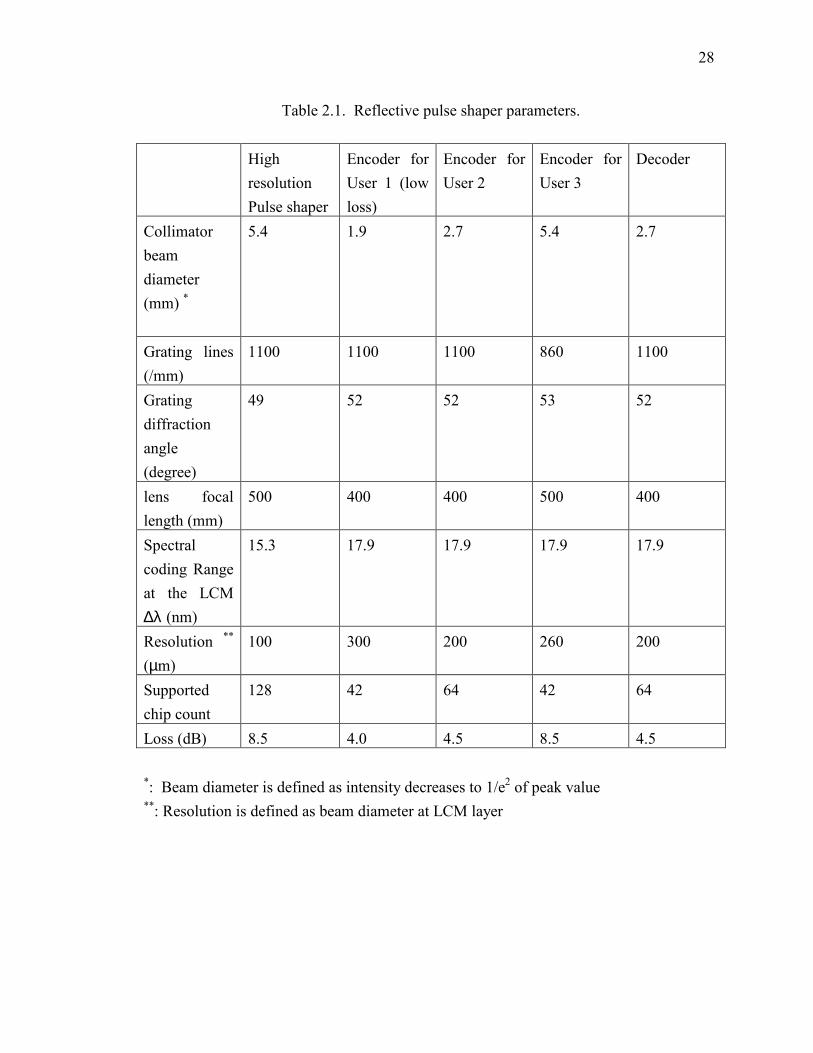
28
Table 2.1. Reflective pulse shaper parameters.
High resolution Pulse shaper
Encoder for User 1 (low loss)
Encoder for User 2
Encoder for User 3
Decoder
Collimator beam diameter (mm) *
5.4
1.9
2.7
5.4 2.7
Grating lines (/mm)
1100 1100 1100 860 1100
Grating diffraction angle (degree)
49 52 52 53 52
lens focal length (mm)
500 400 400 500 400
Spectral coding Range at the LCM ∆λ (nm)
15.3 17.9 17.9 17.9 17.9
Resolution ** (µm)
100 300 200 260 200
Supported chip count
128 42 64 42 64
Loss (dB) 8.5 4.0 4.5 8.5 4.5 *: Beam diameter is defined as intensity decreases to 1/e2 of peak value **: Resolution is defined as beam diameter at LCM layer

29
-15 -10 -5 0 5 10 15Time (ps)
Inte
nsity
(a.u
.)Uncoded
Encoded
-15 -10 -5 0 5 10 15Time (ps)
Inte
nsity
(a.u
.)
Properly decoded
Improperly decoded(A) (B)
-15 -10 -5 0 5 10 15Time (ps)
Inte
nsity
(a.u
.)Uncoded
Encoded
-15 -10 -5 0 5 10 15Time (ps)
Inte
nsity
(a.u
.)
Properly decoded
Improperly decoded(A) (B)
Fig. 2.5. Intensity cross-correlation measurements. (A) uncoded (solid line) and 31 MS encoded (dotted line) pulses. (B) properly decoded (solid line) and improperly decoded
(dotted line) pulses.
Inte
nsity
(a.u
.) Encoded
Uncoded
1535 1540 1545 1550Wavelength (nm)
Properly decoded
1535 1540 1545 1550Wavelength (nm)
Improperly decoded
(A)
(B)
(C)
(D)
Inte
nsity
(a.u
.) Encoded
Uncoded
1535 1540 1545 1550Wavelength (nm)
Properly decoded
1535 1540 1545 1550Wavelength (nm)
Improperly decoded
(A)
(B)
(C)
(D)
Fig. 2.6. Optical spectra measurements. (A) uncoded, (B) 31 MS encoded, (C) properly
decoded and improperly decoded. Optical spectrum analyzer (OSA) resolution: 0.05nm.

30
Temperature: 92.5 OC
1541 1541.5 1542 1542.5 1543Wavelength (nm)
Temperature: 92.5 OC
1541 1541.5 1542 1542.5 1543Wavelength (nm)
1541.5 1542 1542.5 1543Wavelength (nm)
Fig. 2.7. Periodically-poled lithium niobate (PPLN) waveguide second harmonic generation (SHG) phase matching spectrum.
-40 -20 0 20 40 60
Time (ps)
(D)
-40 -20 0 20 40 60Time (ps)
(C)
-40 -20 0 20 40 60
(B)
-40 -20 0 20 40 60
(A)
-40 -20 0 20 40 60
Time (ps)
(D)
-40 -20 0 20 40 60Time (ps)
(C)
-40 -20 0 20 40 60
(B)
-40 -20 0 20 40 60
(A)
Fig. 2.8. Intensity cross-correlation measurements of properly decoded channels 1 to 4 (A
to D respectively) demonstrating the ability to selectively decode any of the four user channels. Channel 4 (D) is the uncoded user.

31
Fig. 2.9. Eye diagrams prior to nonlinear processing (measurement point α in Fig. 3).
Single user properly decoded (A), improperly decoded (B), two users (C), and four users (D). A & B demonstrate that both properly decoded and improperly decoded single user channels look essentially identical on a linear detector. C & D demonstrate that multiple
users can not be adequately separated using linear detection.
Fig. 2.10. Eye-diagrams after nonlinear processing (measurement point β in Fig. 3), at -3dBm per user. (A) Properly decoded channel 1, single user. (B) Improperly decoded
channel 1, single user. (C) Two users system, properly decode channel 1. D) Four users system, properly decode channel 2. A & B demonstrate the large contrast between a
properly and improperly decoded single user channel. C & D demonstrate clear decoding of the desired user in a multiple user system via nonlinear processing.
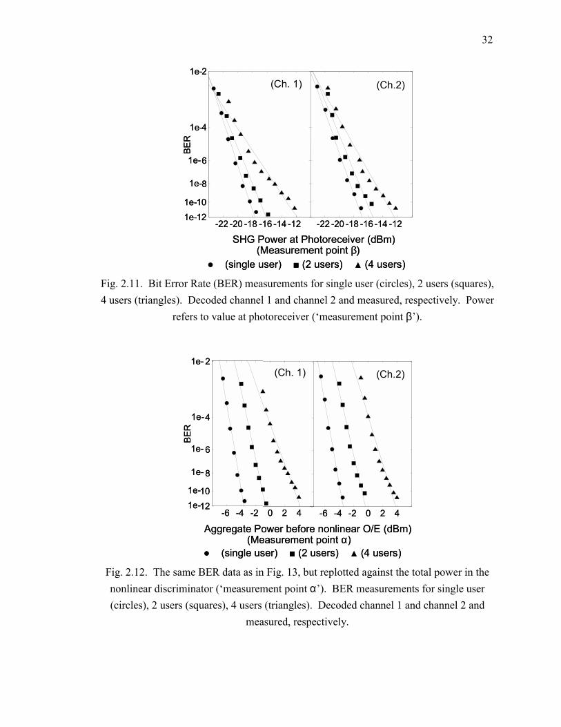
32
-22 -20 -18 -16 -14 -12-22 -20 -18 -16 -14 -12
2
4
6
8
1012
BER
1e-
1e-
1e-1e-
1e-
1e-
(Ch. 1) (Ch.2)
SHG Power at Photoreceiver (dBm)(Measurement point β)
● (single user) ■ (2 users) ▲ (4 users)
-22 -20 -18 -16 -14 -12-22 -20 -18 -16 -14 -12
2
4
6
8
1012
BER
1e-
1e-
1e-1e-
1e-
1e-
(Ch. 1) (Ch.2)
SHG Power at Photoreceiver (dBm)(Measurement point β)
● (single user) ■ (2 users) ▲ (4 users) Fig. 2.11. Bit Error Rate (BER) measurements for single user (circles), 2 users (squares), 4 users (triangles). Decoded channel 1 and channel 2 and measured, respectively. Power
refers to value at photoreceiver (�measurement point β�).
-6 -4 -2 0 2 4
Aggregate Power before nonlinear O/E (dBm)(Measurement point α)
-6 -4 -2 0 2 4
2
4
6
8
1012
BER
1e-
1e-
1e-1e-
1e-
1e-
(Ch. 1) (Ch.2)
● (single user) ■ (2 users) ▲ (4 users)
-6 -4 -2 0 2 4
Aggregate Power before nonlinear O/E (dBm)(Measurement point α)
-6 -4 -2 0 2 4
2
4
6
8
1012
BER
1e-
1e-
1e-1e-
1e-
1e-
(Ch. 1) (Ch.2)
● (single user) ■ (2 users) ▲ (4 users) Fig. 2.12. The same BER data as in Fig. 13, but replotted against the total power in the nonlinear discriminator (�measurement point α�). BER measurements for single user (circles), 2 users (squares), 4 users (triangles). Decoded channel 1 and channel 2 and
measured, respectively.
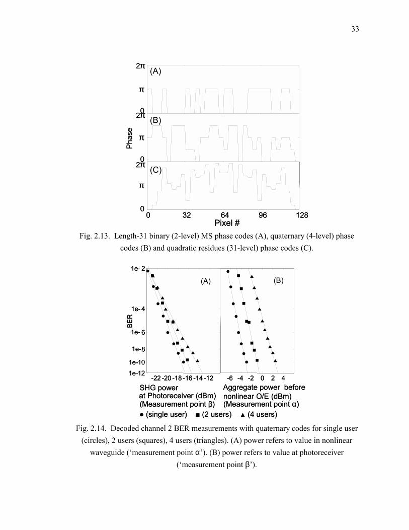
33
0 32 64 96 1280
π
2π0
π
2π0
π
2π
Pixel #
Pha
se
(A)
(B)
(C)
0 32 64 96 1280
π
2π0
π
2π0
π
2π
Pixel #
Pha
se
(A)
(B)
(C)
Fig. 2.13. Length-31 binary (2-level) MS phase codes (A), quaternary (4-level) phase
codes (B) and quadratic residues (31-level) phase codes (C).
-6 -4 -2 0 2 4-22 -20 -18 -16 -14 -12
2
4
6
8
1012
BER
1e-
1e-
1e-1e-
1e-
1e-
Aggregate power before nonlinear O/E (dBm) (Measurement point α)
SHG power at Photoreceiver (dBm) (Measurement point β) ● (single user) ■ (2 users) ▲ (4 users)
(A) (B)
-6 -4 -2 0 2 4-22 -20 -18 -16 -14 -12
2
4
6
8
1012
BER
1e-
1e-
1e-1e-
1e-
1e-
Aggregate power before nonlinear O/E (dBm) (Measurement point α)
SHG power at Photoreceiver (dBm) (Measurement point β) ● (single user) ■ (2 users) ▲ (4 users)
(A) (B)
Fig. 2.14. Decoded channel 2 BER measurements with quaternary codes for single user
(circles), 2 users (squares), 4 users (triangles). (A) power refers to value in nonlinear waveguide (�measurement point α�). (B) power refers to value at photoreceiver
(�measurement point β�).

34
Aggregate power before nonlinear O/E (dBm) (Measurement point α)
SHG power at Photoreceiver (dBm) (Measurement point β) ● (single user) ■ (2 users) ▲ (4 users)
-22 -20 -18 -16 -14 -12
2
4
6
8
1012
BER
-6 -4 -2 0 2 4
1e-
1e-
1e-1e-
1e-
1e-
(A) (B)
Aggregate power before nonlinear O/E (dBm) (Measurement point α)
SHG power at Photoreceiver (dBm) (Measurement point β) ● (single user) ■ (2 users) ▲ (4 users)
-22 -20 -18 -16 -14 -12
2
4
6
8
1012
BER
-6 -4 -2 0 2 4
1e-
1e-
1e-1e-
1e-
1e-
(A) (B)
Fig. 2.15. Decoded channel 2 BER measurements with quadratic residue codes for single user (circles), 2 users (squares), 4 users (triangles). (A) power refers to value in nonlinear
waveguide (�measurement point α�). (B) power refers to value at photoreceiver (�measurement point β�).
Fig. 2.16. Degradation caused by pulse overlapping between users. Eye diagrams for 2 users (channel 1 and 4) with separation (A) 0 ps (B) 10 ps (C) 20 ps (D) 30 ps separation
with decoded channel 1.

35
Signal
NonlinearProcessing
MAI
I
I
NI O/E
Fluctuation
Signal
NonlinearProcessing
MAI
I
I
NI O/E
Fluctuation
Fig. 2.17. Illustration of system degradation caused by pulse overlap between users.
0 20 40 60 80 100 0 20 40 60 80 100
0 20 40 60 80 100 0 20 40 60 80 100
Time (ps)
User #1 User #2
User #3 User #4Pulse channel
0 20 40 60 80 1000 20 40 60 80 100 0 20 40 60 80 1000 20 40 60 80 100
0 20 40 60 80 1000 20 40 60 80 100 0 20 40 60 80 1000 20 40 60 80 100
Time (ps)
User #1 User #2
User #3 User #4Pulse channel
Fig. 2.18. Intensity cross-correlation measurements of properly decoded user #1 to #4, demonstrating the ability to selectively decode any of the four users at 10 Gb/s.
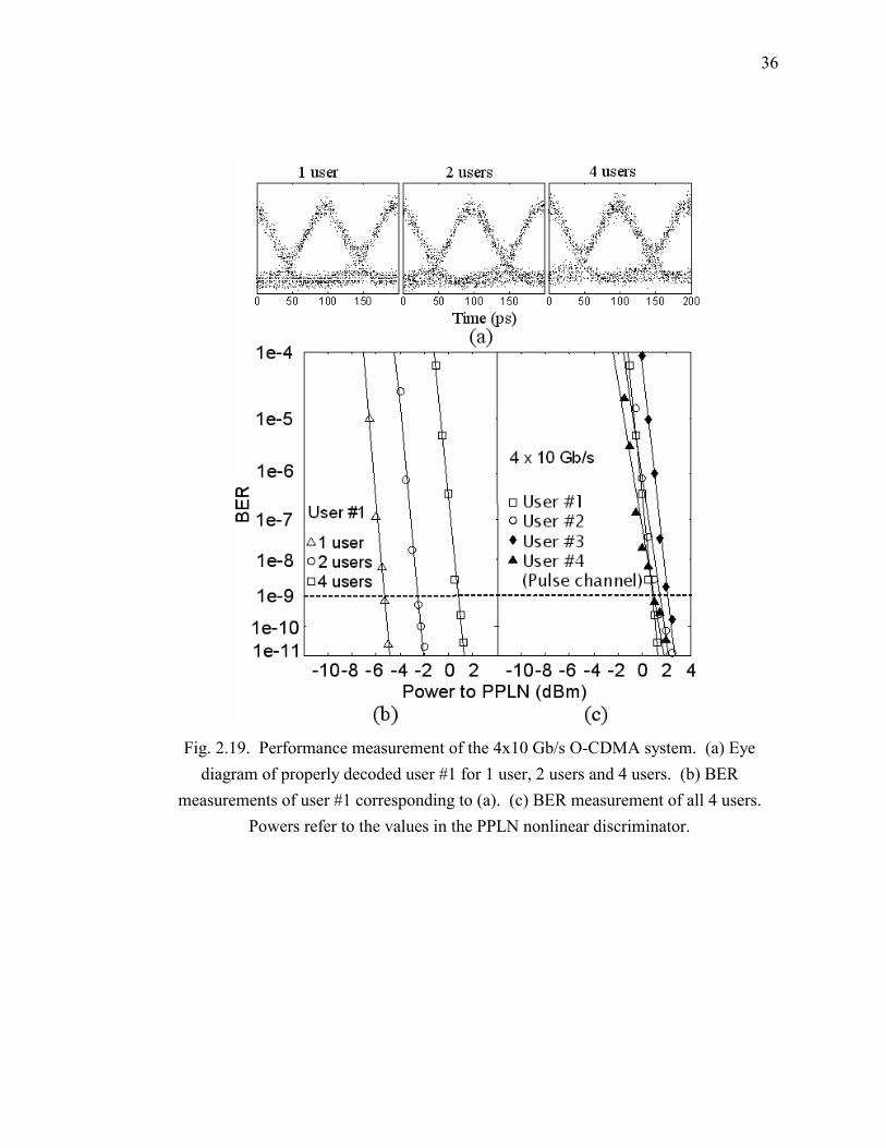
36
Fig. 2.19. Performance measurement of the 4x10 Gb/s O-CDMA system. (a) Eye
diagram of properly decoded user #1 for 1 user, 2 users and 4 users. (b) BER measurements of user #1 corresponding to (a). (c) BER measurement of all 4 users.
Powers refer to the values in the PPLN nonlinear discriminator.

37
Fig. 2.20. BER measurements and eye diagrams of properly decoded user #1 with one
interference user while tuning the user separation. Performance is degraded when 2 users overlap.
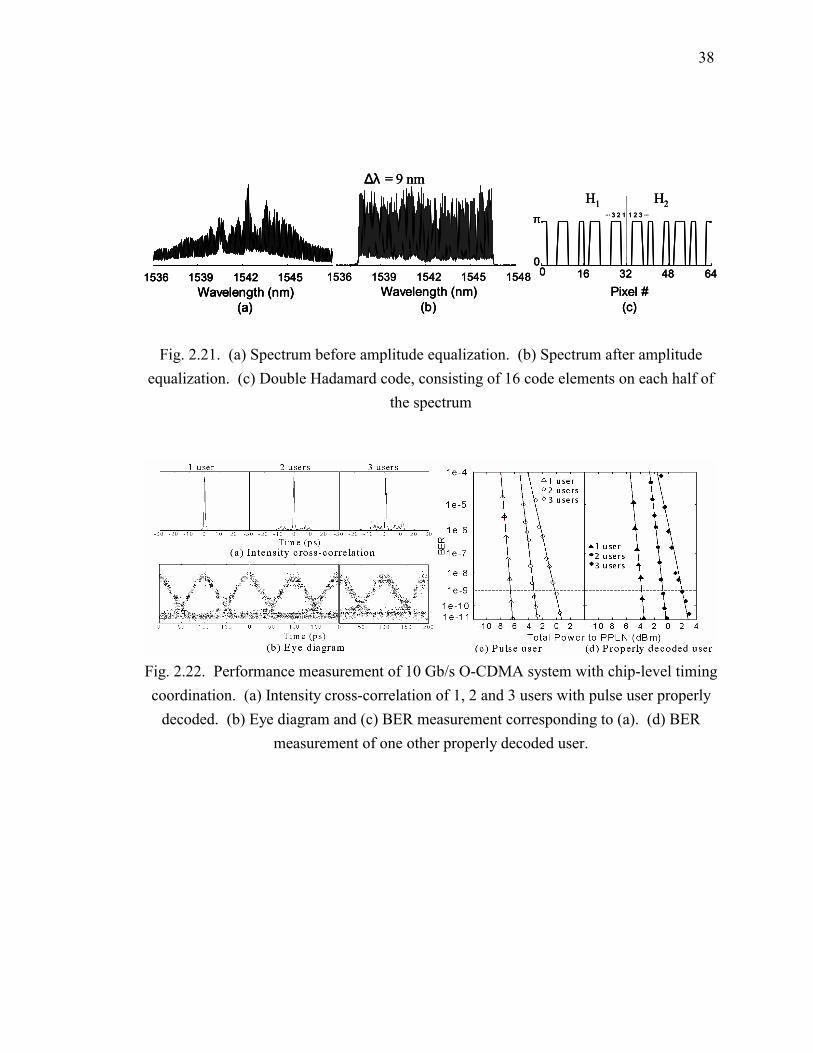
38
16 32 48 64
π
0 0
Pixel #(c)
H1 H2··· 3 2 1 1 2 3 ···
1536 1539 1542 1545 1548Wavelength (nm)
(b)
∆λ = 9 nm
1536 1539 1542 1545Wavelength (nm)
(a)
16 32 48 64
π
0 0
Pixel #(c)
H1 H2··· 3 2 1 1 2 3 ···
16 32 48 64
π
0 0
Pixel #(c)
H1 H2··· 3 2 1 1 2 3 ···
1536 1539 1542 1545 1548Wavelength (nm)
(b)
∆λ = 9 nm
1536 1539 1542 1545Wavelength (nm)
(a)
1536 1539 1542 1545 1548Wavelength (nm)
(b)
∆λ = 9 nm
1536 1539 1542 1545Wavelength (nm)
(a)
1536 1539 1542 1545Wavelength (nm)
(a)
Fig. 2.21. (a) Spectrum before amplitude equalization. (b) Spectrum after amplitude equalization. (c) Double Hadamard code, consisting of 16 code elements on each half of
the spectrum
Fig. 2.22. Performance measurement of 10 Gb/s O-CDMA system with chip-level timing coordination. (a) Intensity cross-correlation of 1, 2 and 3 users with pulse user properly
decoded. (b) Eye diagram and (c) BER measurement corresponding to (a). (d) BER measurement of one other properly decoded user.
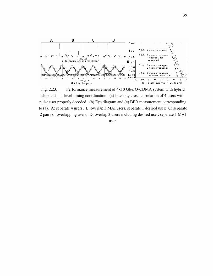
39
Fig. 2.23. Performance measurement of 4x10 Gb/s O-CDMA system with hybrid chip and slot-level timing coordination. (a) Intensity cross-correlation of 4 users with
pulse user properly decoded. (b) Eye diagram and (c) BER measurement corresponding to (a). A: separate 4 users; B: overlap 3 MAI users, separate 1 desired user; C: separate 2 pairs of overlapping users; D: overlap 3 users including desired user, separate 1 MAI
user.
40
3. RECONFIGURABLE ALL-OPTICAL CODE TRANSLATION IN SPECTRALLY PHASE CODED O-CDMA NETWROKS
In this chapter, we describe code translation operation in our O-CDMA testbed
[68]. 3.1 Introduction of Code Translation in O-CDMA Networks
CDMA is well suited for network environments characterized by bursty data and multiple users, and O-CDMA provides the potential to use optical processing to perform certain network operations such as addressing and routing. Reconfigurable O-CDMA coding would allow the number of required codes to be reduced by code-reallocation to share codes among subscribers, while all-optical code-translation would enable the capability to form cascadable and/or routable O-CDMA networks (since modifying the code would be equivalent to modifying the address). Fig. 3.1shows the conceptual diagram of code translation in an O-CDMA network. Suppose the signal encoded by code C1 at a transmitter travels to the destination across one optical path, as shown in the figure. Since multiple users share the fiber transmission medium in O-CDMA networks, C1 might have already been used between certain optical nodes due to the limited code space. If this does happen, code translation has to be employed to resolve the confliction. In this example, code C1 is translated to C2, C3 and C4 respectively at the corresponding optical nodes along the optical path before reaching destination. As a result, code translation is an efficient way to increase user counts and/or reduce the number of required codes by re-using codes in O-CDMA networks. The ability to dynamically translate from one code to another in an O-CDMA network is analogous to dynamic wavelength conversion/switching which is a key capability for reconfigurable wavelength division multiplexed (WDM) networks [69,70].
Code translation in O-CDMA can be implemented via optoelectronic conversion (O/E-E/O) [71] while losing optical transparency. Previous efforts to pursue all optical O-CDMA code translation have been reported in time domain coding [72] and 2-D time/wavelength coding [73]. Both of these works required a complicated nonlinear optical processing scheme with short code lengths (4-8 chips) and the code translators did

41
not support dynamic reconfiguration. Moreover, the previous work only demonstrated single-stage, single user code translation. In this paper, we demonstrate, for the first time to our knowledge, reconfigurable all-optical code translation in a spectrally phase coded O-CDMA testbed. Both 1-stage and 2-stage code translations induce less than 0.9 dB power penalties at each code translation. Multi-stage code translations (greater than two) are investigated via simulation and experimental emulation in a loop pulse shaper, to show the potential of code translations up to several tens of translations. In our spectral phase coding scheme, the code translator is the same apparatus as the O-CDMA encoder/decoder and provides multi-stage code translation in a simple, linear, and delay-free scheme. Code translation is essentially instantaneous, limited only by the propagation time through the free-space apparatus, which is significantly faster than other methods based on optoelectronic conversion [71] or nonlinear optical processing in long fibers [72]. The programmability of the code translation function demonstrated here is a fundamental operation required for efficient reconfiguration of O-CDMA networks, which potentially shows better network performance than its fixed counterpart. Similar improvement was observed when using tunable rather than fixed wavelength conversion in WDM networks [69]. Furthermore, an interference user is included in our code translation demonstration so that the effect of MAI can be evaluated, which is a key issue in any O-CDMA demonstration.
Similar to previous O-CDMA all-optical code translation approaches [72,73], all users will experience code translation in our scheme. It is not possible to independently change the code for different users in the same fiber, which is similar to some of the wavelength conversion techniques in WDM networks. This is a constraint, for example, if only one user is expected to be code translated while keeping other users untouched. However, this could also be a significant advantage in some situations, analogous to simultaneous multi-wavelength conversion in WDM networks [69,70]. 3.2 Principle of Code Translation
In our O-CDMA scheme, an input ultrashort pulse spectrum A(ω) is spectrally phase coded as A(ω) exp{jC(ω)} and broadened to a pseudonoise waveform in the time domain, where C(ω) is the spectral phase code C(ω)={C0(ω0),C1(ω1),...,CN-1(ωN-1)}. Here Ci(ωi) represents the i-th spectral code chip in a code sequence of length N, which the encoder applies to a small band of frequencies centered at angular frequency ωi, i = 0,1,...,(N-1). For M-ary phase coding, the phase in any particular chip is allowed to take on M possible values, given by

42
2 , 0,1,..., ( 1).ii i
kC k MMπ= = − (3.1)
When ki = 0 for all Ci no phase modulation is applied and the pulses remain uncoded. Since the code translation devices are the same as encoder/decoder, all of them can be uniformly treated as coders for notation convenience. An optical path with L coders consists of 1 encoder, (L-2) code translators and 1 decoder, corresponding to (L-2)-stage code translation. For proper decoding after passing through all of the stages, the accumulated spectral phase modulation for each code chip becomes equal to an integer multiple of 2π and properly decoded waveform is converted back to a short pulse (same temporal shape as the original input pulse); mathematically
)2(mod01
π=∑=
L
p
pC (3.2)
where Cp is the phase code applied by the p-th coder, p = 1,2,...,L. Note that (2) represents a chip-by-chip summation, which can be broken into a set of N equations explicitly
10 (mod 2 ), 0,1,..., ( 1)
Lp
ip
C for all i Nπ=
= = −∑ (3.3)
Where piC is the i-th chip of phase code Cp applied by the p-th coder. In the special case
of L = 2, it reduces to the familiar simple encoder/decoder pair without code translation, where codes for the encoder/decoder are conjugate when properly decoded.
On the other hand, at a translator knowing the incoming and outgoing waveforms with phase code Cin and Cout respectively, the code applied to code translator CT can be calculated as
)2(mod πinoutT CCC −= (3.4)
Again, (4) is based on chip-by-chip operation. Note that the code Cout for an outgoing waveform differs from the code CT applied by code translator. For successful code translation, the translated outgoing pseudonoise waveform with phase code Cout shows distinct fine structure from the incoming waveform with phase code Cin.
CDMA systems typically utilize specific code families, where each code within the code family is known to exhibit desirable properties such as pseudorandom properties or low cross-correlation and auto-correlation side-lobes. Furthermore, many popular code families known from the communications literature are closed under summation, in the sense that for any two member phase codes Ca and Cb, the phase codes (Ca ± Cb modulo 2π) which are formed via chip-by-chip operation are also a member of the same

43
code family. Examples of code families with good pseudorandom properties and that are closed under summation include M-sequences (a binary code, M = 2) and the family A sequence (a quaternary code, M = 4) [65]. Therefore, in our scheme not only all codes exhibited by the coded waveforms along the optical path (Cin, Cout), but also all codes used by the encoder, translators, and decoder (Cp, CT) remain members of the original code family. These properties will be desirable for spectrally phase coded O-CDMA networks, since they simplify the code translator design and configuration (essentially the same as encoder/decoder) and guarantee that the resultant MAI (improperly decoded) signal retains good pseudorandom properties. Both binary codes and quaternary codes from the communications literature have been used for successful system demonstrations as shown in chapter 2 and are suitable for application to code translation. The discussion of code translation also applies to orthogonal binary codes often used in O-CDMA system, e.g. Hadamard codes [62]. Hereafter, quaternary codes from the family A sequence (M = 4) are used unless otherwise specified. 3.3 1-Stage Code Translation Experiment
A schematic diagram of a single-stage O-CDMA code translation demonstration is shown in Fig. 3.2. An actively mode-locked fiber laser followed by dispersion decreasing fiber soliton compressor producing nearly transform-limited ~0.4 ps pulses at ~10 GHz centered near 1542 nm is used as the pulse source. A 2.5 Gb/s PRBS 223-1 data stream is impressed on the laser output with an intensity modulator (4 pulses in each bit) and then split to generate both desired and interference users. For each user, the modulated ultrashort pulses are input into programmable spectral phase encoders � fiber coupled Fourier Transform pulse shapers. User channels are independently controlled to equalize their powers and to obtain identical polarizations in order to correctly evaluate the effect of MAI. The output of each user path is de-correlated by a fiber delay line and then combined at the programmable code translator � the third pulse shaper. The receiver consists of a decoder � the fourth pulse shaper - used to select the desired user to decode, an optical amplifier, a highly sensitive fiber pigtailed periodically-poled lithium niobate (PPLN) waveguide to perform the nonlinear discrimination function based on second harmonic generation (SHG), and a 2.4 GHz bandwidth photoreceiver, adapted from 10 Gb/s Ethernet, operating at the second harmonic wavelength of 0.77 µm. Further, appropriate lengths of dispersion compensating fiber (DCF) are used to compensate the dispersion of the system. Only single mode fiber (SMF) and DCF are used in our experiments; polarization-maintaining (PM) fiber is not employed.
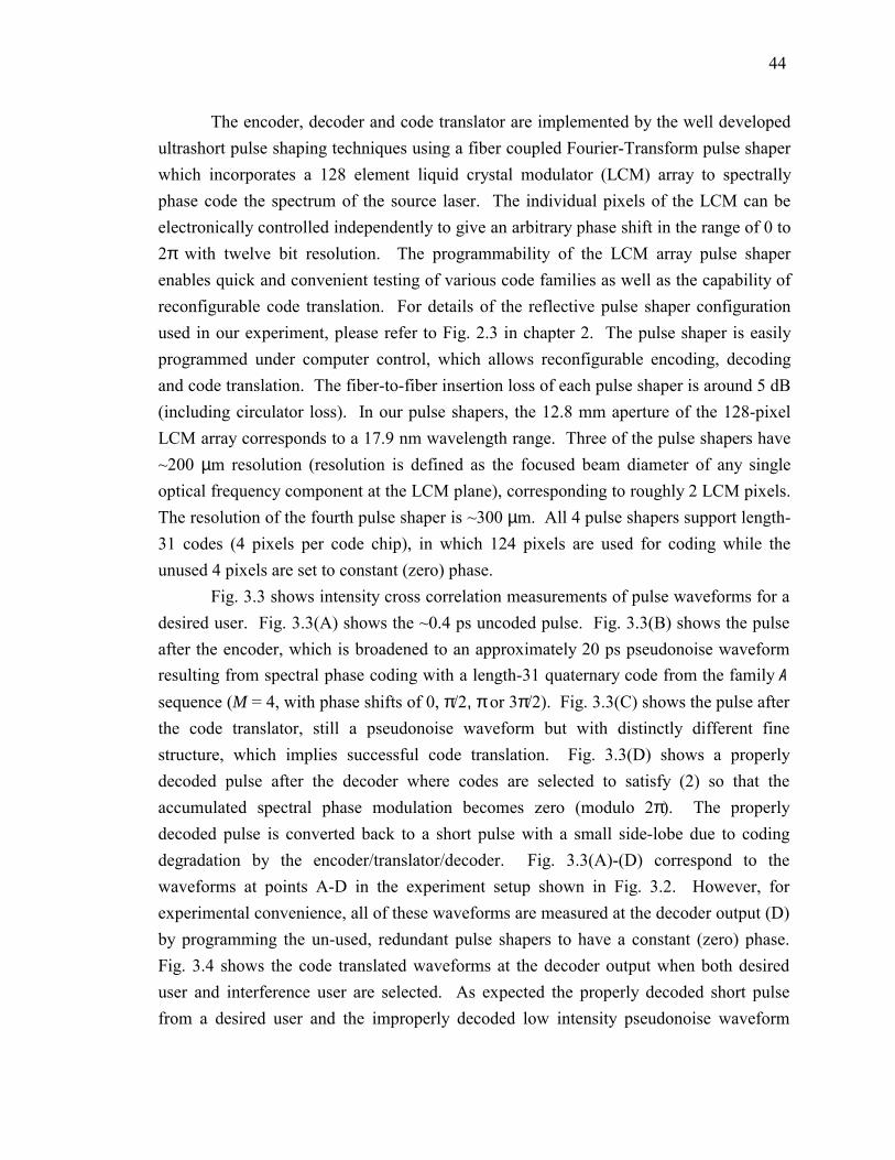
44
The encoder, decoder and code translator are implemented by the well developed ultrashort pulse shaping techniques using a fiber coupled Fourier-Transform pulse shaper which incorporates a 128 element liquid crystal modulator (LCM) array to spectrally phase code the spectrum of the source laser. The individual pixels of the LCM can be electronically controlled independently to give an arbitrary phase shift in the range of 0 to 2π with twelve bit resolution. The programmability of the LCM array pulse shaper enables quick and convenient testing of various code families as well as the capability of reconfigurable code translation. For details of the reflective pulse shaper configuration used in our experiment, please refer to Fig. 2.3 in chapter 2. The pulse shaper is easily programmed under computer control, which allows reconfigurable encoding, decoding and code translation. The fiber-to-fiber insertion loss of each pulse shaper is around 5 dB (including circulator loss). In our pulse shapers, the 12.8 mm aperture of the 128-pixel LCM array corresponds to a 17.9 nm wavelength range. Three of the pulse shapers have ~200 µm resolution (resolution is defined as the focused beam diameter of any single optical frequency component at the LCM plane), corresponding to roughly 2 LCM pixels. The resolution of the fourth pulse shaper is ~300 µm. All 4 pulse shapers support length-31 codes (4 pixels per code chip), in which 124 pixels are used for coding while the unused 4 pixels are set to constant (zero) phase.
Fig. 3.3 shows intensity cross correlation measurements of pulse waveforms for a desired user. Fig. 3.3(A) shows the ~0.4 ps uncoded pulse. Fig. 3.3(B) shows the pulse after the encoder, which is broadened to an approximately 20 ps pseudonoise waveform resulting from spectral phase coding with a length-31 quaternary code from the family A sequence (M = 4, with phase shifts of 0, π/2, π or 3π/2). Fig. 3.3(C) shows the pulse after the code translator, still a pseudonoise waveform but with distinctly different fine structure, which implies successful code translation. Fig. 3.3(D) shows a properly decoded pulse after the decoder where codes are selected to satisfy (2) so that the accumulated spectral phase modulation becomes zero (modulo 2π). The properly decoded pulse is converted back to a short pulse with a small side-lobe due to coding degradation by the encoder/translator/decoder. Fig. 3.3(A)-(D) correspond to the waveforms at points A-D in the experiment setup shown in Fig. 3.2. However, for experimental convenience, all of these waveforms are measured at the decoder output (D) by programming the un-used, redundant pulse shapers to have a constant (zero) phase. Fig. 3.4 shows the code translated waveforms at the decoder output when both desired user and interference user are selected. As expected the properly decoded short pulse from a desired user and the improperly decoded low intensity pseudonoise waveform
45
from an interference user are clearly observed. The interference noise will be suppressed by the following nonlinear optical processing in the O-CDMA system testbed. Note that a slot-level timing coordination scheme is applied to separate the desired user and interference user by ~40 ps to avoid beat noise caused by their interaction.
Fig. 3.5 shows eye diagrams and corresponding bit error rate (BER) curves versus total power in the nonlinear discriminator. The results without code translation are obtained by programming the code translator to have a constant phase; the desired user is still properly decoded by the appropriate code choice at the decoder. To demonstrate effective MAI suppression, results for single user operation are also presented for comparison. In both situations, code translation induces less than 0.6 dB power penalty, which we attribute to coding degradation added by the code translator. Small power penalties point out the feasibility of multi-stage code translation. The 3.5 dB power difference between single user and two users BER curves indicates 0.5 dB power penalty caused by MAI since 3 dB power difference is simply due to the doubling of the number of users at the nonlinear discriminator. We attribute this 0.5 dB power penalty to the finite interference suppression of the nonlinear discriminator. The power requirement of less than -3 dBm per user at BER=10-9 provides substantial margin for scaling to higher bit rates and larger user counts. 3.4 2-Stage Code Translation Experiment
Fig. 3.6 shows the experimental apparatus for 2-stage code translation, which is similar to the previous 1-stage code translation. One more pulse shaper is added as the second code translator. The desired user is combined with an uncoded pulse interference user after the first stage code translation. As a result, the desired user and the interference user experience different code translation paths and translation times emulating what would happen in an actual network environment. One more optical amplifier is added for loss compensation.
Fig. 3.7(a) shows intensity cross correlation measurements of pulse waveforms for the desired user: (A) uncoded (B) encoded (C) translated once (D) translated twice and (E) properly decoded pulses. Fig. 3.7(b) shows the length-31 quaternary phase codes applied to the encoder, code translator 1, code translator 2, and decoder. Translated pulses remain pseudonoise waveforms but with distinct fine temporal structures. The encoded and translated once pseudonoise waveforms are different from the previous single-stage translation experiment because different quaternary codes are applied. The properly decoded pulse is converted back to a short pulse, demonstrating successful 2-

46
stage code translation and decoding. Again, figures (A)-(E) in Fig. 3.7(a) correspond to waveforms at points A-E as shown in the experiment setup of Fig. 3.6, but all waveforms are measured at the point E by programming un-used pulse shapers to have a constant phase as we did previously. Again, the desired user and interference user are separated by ~40 ps (not shown).
Fig. 3.8 shows BER curves for 2-stage code translation. The results without code translation are obtained by programming both code translators to have a constant phase. The results with code translation once (not from previous 1-stage experiment) are obtained by programming the code translator 2 to have a constant phase. The desired user is still properly decoded by choosing appropriate codes at the decoder for both cases. To demonstrate effective MAI suppression, results for a single user (without interference) are also shown for comparison. In both situations, less than 0.9 dB power penalty is observed at each code translation. Again, the power requirement of less than -3 dBm per user at BER=10-9 provides substantial margin for scaling to higher bit rates and larger user counts. Fig. 3.8 shows better BER performance for a single user (in absence of interference) compared to the 1-stage translation experiment in Fig. 3.5, which may be attributed to better dispersion compensation in the 2-stage translation experiment. On the other hand, results for 2 users show similar performance, possibly because the interference user is only present in one code translation stage and therefore experiences less coding loss than the desired user. Thus, compared to the one stage translation experiment, the ratio of interference to desired user should be somewhat larger in the 2-stage translation experiment. 3.5 Pulse Degradation Caused by Coding
According to the pulse intensity cross-correlation measurement, a properly decoded pulse is converted back to a short pulse, but is degraded with small side-lobes and reduced in peak intensity. In this section, pulse degradation caused by the coding process is investigated in detail based on experiment and simulation.
We use the same 2-stage code translation experimental setup shown in Fig. 3.6 with 4 cascaded pulse shapers (without an interference user). Fig. 3.9(a) shows the intensity cross-correlation measurement for a properly decoded pulse after a different number of coding operations. Appropriate quaternary code combination is applied to enable proper decoding for each case. All of the pulses are measured at point E, while un-used pulse shapers are set to have a constant phase: (A) zero coding operations - all of the 4 pulse shapers are set to a constant phase corresponding to an uncoded pulse; (B) 2
47
coding operations (encoder→decoder) - the code translator 1 and 2 shapers are set to a constant phase corresponding to a properly decoded pulse by the encoder/decoder pair; (C) 3 coding operations (encoder→translator 1→decoder) - the code translator 2 shaper is set to a constant phase corresponding to single-stage code translation; (D) 4 coding operations (encoder→translator 1→translator 2→decoder) corresponding to 2-stage code translation. Note that we need at least 2 shapers (encoder and decoder) to recover the original short pulse. From this data, it is clear that pulse degradation increases with the number of coding operations, showing lower peak intensity and larger side-lobes. Pulse degradation is mainly due to the spectral phase coding process in encoder/translators/decoder. Fig. 3.9(b) shows the measured optical spectra corresponding to the time domain traces shown in Fig. 3.9(a). The spectrum for the uncoded pulse (A) shows ~17.9 nm spectral coding range across the 128 LCM pixels. Clear spectral dips are observed in the spectra of (B-D) whenever a phase transition (0, π/2, π, 3π/2) occurs in the spectrum, which explains the pulse degradation including coding loss, side-lobes and slight pulse broadening. In this example, after 4 coding operations (2-stage code translation), all 31 spectral dips occur for length-31 quaternary codes. If a phase transition occurs at the position of an already existing dip, the spectral dip becomes wider and deeper. Therefore, as the number of coding operations increases, the number of spectral dips increases and/or the dips become wider and deeper. The spectral dips result from diffraction effects arising from the frequency components falling at phase transition regions of the LCM in the pulse shaper, which has been quantitatively clarified previously [60].
As mentioned above, we attribute the pulse degradation to spectral dips caused by the diffraction effects. Simulation is performed to confirm this argument based on the theoretical model in [60]. Only the spectral phase coding effect is considered in our simulation. The measured uncoded spectrum (Fig. 3.9(b)(A)) is used as the input spectrum (assume no initial spectral phase) to our simulation. The measured pulse shaper resolutions are used in the simulation: 300 µm resolution for the translator 2, and 200 µm resolution for the other 3 pulse shapers. Fig. 3.9(c) and (d) show the simulation results of pulse intensities and spectra corresponding to Fig. 3.9(a) and (b). The spectral dips are in excellent agreement with the experimental results. Pulse peak intensity reduction and side-lobe appearance are consistent with experiments. Pulse widths of simulations are narrower than those of experiments because experimental measurements yield pulse intensity cross-correlation instead of intensity itself. More noticeably, peak intensities of simulations are lower than those of experiments where coding losses are partially

48
compensated by optical amplifiers operated in the saturation regime, an effect that is not considered in our simulation. This also explains why the decoded pulse peak intensity in the single-stage translation experiment (Fig. 3.3(D)) is lower than the result shown in Fig. 3.9(a)(C) since one more optical amplifier is used in the setup. The details of the side-lobes after 4 coding operations are investigated through both experiment and simulation, as shown in Fig. 3.10, where a second order side-lobe arises. The intensity scales are adjusted for easy comparison. First order and second order side-lobes are located at ±14.3 ps and ±28.6 ps, respectively. The side-lobe positions and relative amplitudes agree well between simulation and experiment. The positions of side-lobes can also be calculated in a simple way: each code chip occupies a bandwidth of 17.9/128×4=0.56 nm (69.9 GHz), which is the inverse of the position of the first order side-lobe at 14.3 ps.
To quantify further the comparison between experiment and simulation, we first calculate the normalized peak intensity of a properly decoded pulse versus the number of coding operations, as shown in Fig. 3.11. As mentioned previously, experimental peak intensities are higher than simulation because the coding loss is partially compensated by optical amplifiers working in saturation regime. Since the pulse peak intensity reduction can be compensated by optical amplifiers, it may not be a good indicator of pulse degradation. On the other hand, the agreement of side-lobes between experiment and simulation in Fig. 3.10 prompts us to characterize pulse degradation using the side-lobes. Fig. 3.11 also shows the ratios of side-lobe (first order) energy to total pulse energy, which are not affected by optical amplifiers. The side-lobe energies are measured and calculated by integrating the side-lobes of the waveforms. The experimental results agree well with simulations considering experimental uncertainties.
This discussion has centered on desired user (properly decoded short pulse) degradation caused by code translation. A closely related issue is the effect on the interference user (improperly decoded pseudonoise waveform) or users of passing through the code translators. After code translation, the interference user is coded by another code, with almost the same characteristics as the originally encoded (broadened pseudonoise) waveform. The only difference is that there are more spectral dips (and/or wider and deeper dips) caused by code translation, similar to what is experienced by the desired user after code translation. Such spectral dips on the interference user are associated with loss, which reduces the MAI power in the system. Although the spectral dips may also introduce some distortion onto broadened pseudonoise (MAI) waveforms, such slight distortion is not expected to significantly affect the suppression of improperly decoded pseudonoise signals at the receiver / nonlinear discriminator. Overall, with

49
increasing number of spectral dips and loss onto the interference user, there should be a slight benefit (rather than a negative effect) to O-CDMA system operation, since the MAI power becomes smaller. On the other hand, for the desired user, the spectral dip effect caused by code translation has a negative impact on system performance, as discussed in previous paragraphs. Overall, we believe that the degradation effect on the desired user due to passing through the code translators is more important than the effect of such translation on the MAI. Therfore, we have focused our attention in this thesis on the effects of such degradation on the desired user. This is a conservative approach, since the effects we are ignoring, i.e., the reduction in MAI power, would be expected to mitigate in part the reduction in desired user intensity. 3.6 Multi-Stage Code Translation 3.6.1 Simulation of Multi-Stage Code Translation
As we have observed in an experimental example, after 4 coding operations (2-stage code translation), all 31 spectral dips occur for length-31 quaternary codes (one dip comes from the spectral phase change between coded pixels and the unused 4 pixels). We may expect that pulse degradation will show saturation behavior in multi-stage code translation with a large number of coding operations since all dips already occur after the first few coding operations (although spectral dips become wider and deeper during additional coding operations). We first quantitatively investigate multi-stage code translation through simulation in the same way as we did in the previous section. Fig. 3.12(a) shows normalized peak intensity of a properly decoded pulse versus the number of coding operations. All pulse shapers have identical resolution, in which 100 µm, 200 µm or 300 µm resolutions are used in the calculations, respectively. A larger reduction of pulse peak intensity occurs for the first few coding operations, but less reduction happens for additional coding operations as predicted by qualitative analysis. Pulse peak intensity reduction largely depends on the shaper resolution, which is reduced to 6.0% of the peak value after 30 coding operations for 300 µm resolution, but improved to 56.0% of the peak value for 100 µm resolution. Specific codes applied to all shapers also affect simulation results. Two examples are presented for 100 µm resolution using two sets of quaternary codes, which only shows a slight difference and essentially the same profile. Fig. 3.12(b) shows the ratio of side-lobe (first order) energy to total pulse energy. Again, degradation saturation behavior is observed. Side-lobe energy also largely depends on the shaper resolution, which reaches 49.3% of total pulse energy after 30 coding operations for 300 µm resolution, but is only 13.5% of total pulse energy for 100 µm

50
resolution. On the other hand, note that we have achieved satisfactory system performance under a similar degradation condition in the 2-stage code translation experiment where the side-lobe energy is 14.7% of total pulse energy, as shown in Fig. 3.11. As a result, the agreement between our experiment and simulation for 1- and 2-stage code translation together with simulation for multi-stage code translation shows the potential of several tens of code translations utilizing high resolution pulse shapers. 3.6.2 Experimental Emulation of Multi-Stage Code Translation: Pulse Shaper in a Loop
To emulate multi-stage code translations without the need for a large number of pulse shapers, we proposed a scheme to emulate this process � a pulse shaper in a closed loop where a portion of the shaper output is fed back to the input so as to experience multiple passes through the shaper [74], as shown in Fig. 3.13. This loop scheme allows testing of the multi-stage code translation process in a simple and convenient set-up. In actual O-CDMA networking applications, code translation would instead take place in distinct pulse shapers located at different nodes as demonstrated in the previous sections. The same laser source described earlier is used and all fiber links are dispersion compensated using an appropriate combination of SMF and DCF. A reflective pulse shaper is inserted into the closed loop to permit multiple coding. After the pulse shaper, a portion of the coded output is amplified by an optical amplifier and re-injected into the shaper through the input coupler.
For the pulse shaper in a loop, code Co is imposed onto the spectrum during each of n passes through the shaper. Therefore the output waveform after n passes corresponds to another spectral phase code nCo due to the identical code in all n passes. Whenever the accumulated spectral phase modulation for each code chip becomes equal to an integer multiple of 2π the pulse shaper produces a properly decoded pulse (same temporal shape as the original input pulse), so that mathematically,
)2(mod0 π=onC (3.5)
Similar to Eq.(2), Eq.(5) is based on chip-by-chip operation. Actually Eq.(5) is a special case of Eq. (2), where L = n and identical code Co is used by all coders. For M-ary phase coding, where the phase in any particular chip is allowed to take on M possible values given by Eq. (1), Eq. (5) is satisfied whenever n is an integer multiple of M. When the number of passes n is not equal to a multiple of M, according to the number of passes n

51
modulo M, the pulse shaper output corresponds to a set of (M−1) distinct pseudonoise waveforms, indicating multiple code translated waveforms. Fig. 3.14 shows intensity cross correlation measurements of the output of the closed loop pulse shaper. The numbers labeling the pulses represent the number of passes (n) through the shaper. The delay through the loop is fine-tuned using a fiber stretcher to give an apparent advancement of approximately 15 ps per pass (relative to the 100 ps periodicity arising from the 10 GHz laser repetition rate). For no phase coding (the shaper is set at a constant phase), exponentially decaying pulse trains (with essentially identical shape) are observed, as shown in Fig. 3.14(a). The attenuation corresponds to a net loop loss of ~3 dB per pass. The peaks corresponding to the first eight passes through the pulse shaper are visible. Since only one pulse shaper (thus one code) is used in the closed loop, it is not feasible to properly decode the pulse using a combination of distinct codes in the loop shaper for multi-stage code translation as demonstrated in the previous section. However, note that it is still a valid code translation demonstration even if all pulse shapers use one identical code because each translated pulse exhibits distinct waveforms and represents a distinct code. To illustrate this sort of code translation using one identical code in loop shaper, we incorporate 2-level (M = 2, binary) and 3-level (M = 3) codes as well as 4-level (M = 4, quaternary) code used above. Length-31 code chips are used for all three cases. For a 2-level (0, π) M-sequence code, the output pulses are broad noise-like waveforms after odd numbers of passes, while they are decoded back to their original shape after even numbers of passes, as shown in Fig. 3.14(b). Three complete encoding-decoding cycles can be observed. This clearly demonstrates the cascadable nature of the encoding-decoding process. Although for the 2-level code one may consider the experiment as cascaded identical encoding/decoding operations rather than code translation, the capability to properly decode back to a short pulse after 6 shaper passes is still demonstrated. To some extent, this could be considered as a generalized 4-stage code translation if the all-zero (mod 2π) spectral phase code is also treated as a code. Fig. 3.14(c) shows results obtained using a 3-level (0, 2π/3, 4π/3) code where the phases of each chip are randomly selected. Two distinct encoded waveforms appear at the delay positions corresponding to n = 1, 4 and to n = 2, 5, respectively, while decoded short pulses appear at n = 3, 6. This corresponds to two cycles of 1-stage code translation using one identical code. Or similar to (b), this could be considered as a generalized 4-stage code translation. For a 4-level (0, π/2, π, 3π/2) code, three different encoded waveforms are observed before the pulse is successfully decoded, as shown in Fig. 3.14(d), which corresponds to 2-stage code translation using one identical code. These results show that
52
a pulse could be properly decoded after going through as many as 6 pulse shapers (loop loss and 100 ps periodicity limit us from detecting more), proving the feasibility of multi-stage code translation application. The fundamental limitation of the number of code translation comes from the coding degradation as investigated above; nevertheless, several tens of code translations should be possible as shown in our simulation results.
In an all-optical code translation scheme, all users will experience code translation. This could be a significant advantage, analogous to multi-wavelength conversion in WDM networks [69,70]. In certain network applications, it is desirable that only one user is expected to be code translated while keeping other users untouched. In such a situation, the target user has to be separated from other users, translated to a new code and inserted back to the network, which is a combination of add/drop and code translation functionalities in an O-CDMA network. An add/drop scheme has been proposed [75] for ultrashort pulse spectrally phase coded O-CDMA, but its implementation still remains a challenge.

53
Subnet/UserSubnet/UserSubnet/UserSubnet/User
RoutingRoutingRoutingRouting
OOOO----CDMA NetworkCDMA NetworkCDMA NetworkCDMA Network
Optical Path
RoutingRoutingRoutingRouting
Subnet/UserSubnet/UserSubnet/UserSubnet/User
Subnet/UserSubnet/UserSubnet/UserSubnet/User
Subnet/UserSubnet/UserSubnet/UserSubnet/User
Subnet/UserSubnet/UserSubnet/UserSubnet/User
Subnet/UserSubnet/UserSubnet/UserSubnet/User
C1C2
C3C4
(b)
Subnet/UserSubnet/UserSubnet/UserSubnet/UserSubnet/UserSubnet/UserSubnet/UserSubnet/User
RoutingRoutingRoutingRouting
OOOO----CDMA NetworkCDMA NetworkCDMA NetworkCDMA Network
Optical Path
RoutingRoutingRoutingRouting
Subnet/UserSubnet/UserSubnet/UserSubnet/UserSubnet/UserSubnet/UserSubnet/UserSubnet/User
Subnet/UserSubnet/UserSubnet/UserSubnet/UserSubnet/UserSubnet/UserSubnet/UserSubnet/User
Subnet/UserSubnet/UserSubnet/UserSubnet/UserSubnet/UserSubnet/UserSubnet/UserSubnet/User
Subnet/UserSubnet/UserSubnet/UserSubnet/UserSubnet/UserSubnet/UserSubnet/UserSubnet/User
Subnet/UserSubnet/UserSubnet/UserSubnet/User
C1C2
C3C4
(b) Fig. 3.1. Conceptual diagram of all-optical code translation in an O-CDMA network.
10G Ethernet Receiver
PPLN (SHG)
10GHz 400fs Pulse
Programmable Spectral Phase
Encoder
Programmable Spectral Phase
Decoder
EDFA2.5 GHzMod
PRBS 223-1
Nonlinear O/E
Desired user
Interference user
Programmable Spectral Phase Code Translator
A B C D
3
2
41
10G Ethernet Receiver
PPLN (SHG)
10GHz 400fs Pulse
Programmable Spectral Phase
Encoder
Programmable Spectral Phase
Decoder
EDFA2.5 GHzMod
PRBS 223-1
Nonlinear O/E
Desired user
Interference user
Programmable Spectral Phase Code Translator
A B C D
3
2
41
Fig. 3.2. Experimental apparatus for 1-stage code translation
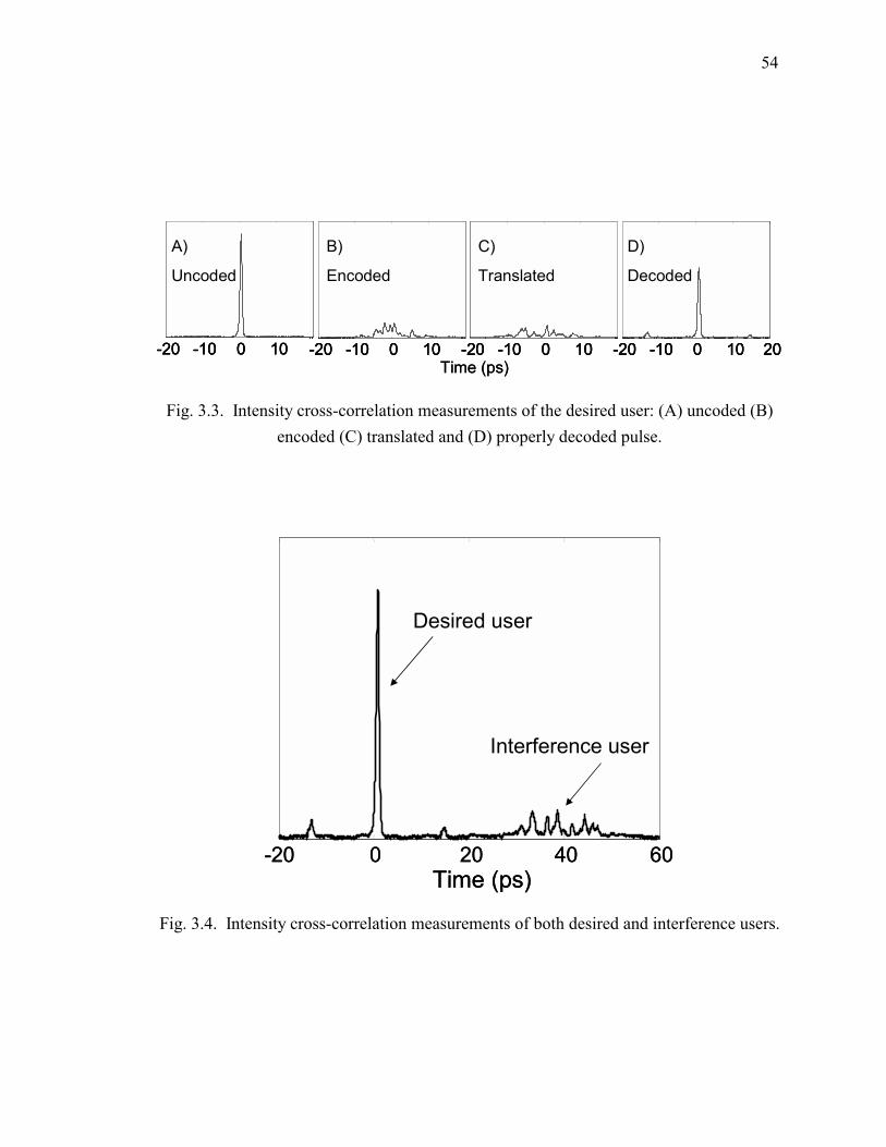
54
-20 -10 0 10 -20 -10 0 10 -20 -10 0 10 -20 -10 0 10 20Time (ps)
A)
Uncoded
B)
Encoded
C)
Translated
D)
Decoded
-20 -10 0 10-20 -10 0 10 -20 -10 0 10-20 -10 0 10 -20 -10 0 10-20 -10 0 10 -20 -10 0 10 20-20 -10 0 10 20Time (ps)
A)
Uncoded
B)
Encoded
C)
Translated
D)
Decoded
Fig. 3.3. Intensity cross-correlation measurements of the desired user: (A) uncoded (B) encoded (C) translated and (D) properly decoded pulse.
-20 0 20 40 60Time (ps)
Desired user
Interference user
-20 0 20 40 60Time (ps)
Desired user
Interference user
Fig. 3.4. Intensity cross-correlation measurements of both desired and interference users.
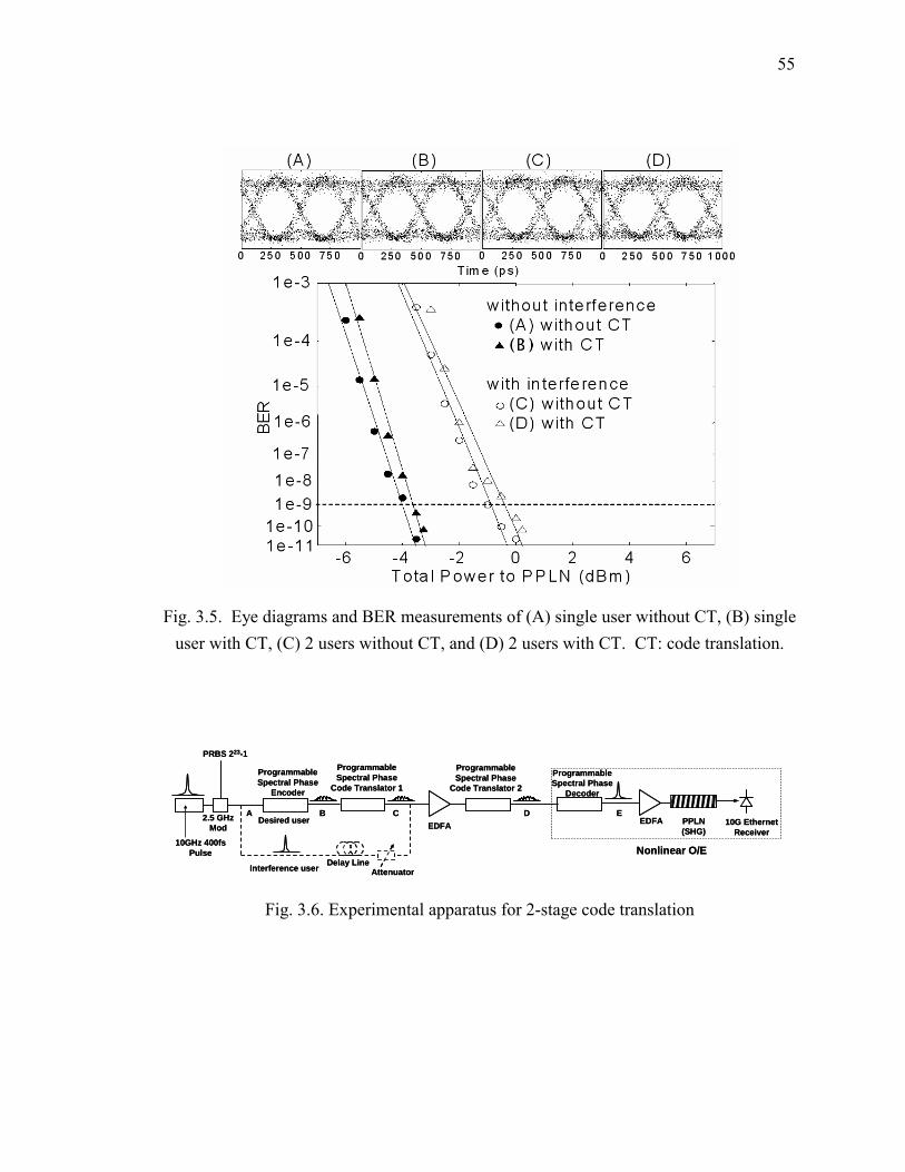
55
Fig. 3.5. Eye diagrams and BER measurements of (A) single user without CT, (B) single user with CT, (C) 2 users without CT, and (D) 2 users with CT. CT: code translation.
10G Ethernet Receiver
PPLN (SHG)
10GHz 400fs Pulse
Programmable Spectral Phase
Encoder
Programmable Spectral Phase
Decoder
EDFA2.5 GHzMod
PRBS 223-1
Nonlinear O/E
Programmable Spectral Phase
Code Translator 1
Programmable Spectral Phase
Code Translator 2
Desired user
Interference user Delay LineAttenuator
EDFAA B C D E
Fig. 3.6. Experimental apparatus for 2-stage code translation

56
-20 -10 0 10 20-20 -10 0 10 -20 -10 0 10 -20 -10 0 10
A)
Uncoded
B)
Encoded
C)
Translated Once
D)
Translated Twice
E)
Decoded
Time (ps)-20 -10 0 10
(a)
0 32 64 9600 32 64 96
π
Phas
e (ra
d)
2π
0 32 64 96Pixel #
0 32 64 96 128
Encoder Translator 1 Translator 2 Decoder
(b)
-20 -10 0 10 20-20 -10 0 10 -20 -10 0 10 -20 -10 0 10
A)
Uncoded
B)
Encoded
C)
Translated Once
D)
Translated Twice
E)
Decoded
Time (ps)-20 -10 0 10
(a)
-20 -10 0 10 20-20 -10 0 10 20-20 -10 0 10-20 -10 0 10 -20 -10 0 10-20 -10 0 10 -20 -10 0 10-20 -10 0 10
A)
Uncoded
B)
Encoded
C)
Translated Once
D)
Translated Twice
E)
Decoded
Time (ps)-20 -10 0 10-20 -10 0 10
(a)
0 32 64 9600 32 64 96
π
Phas
e (ra
d)
2π
0 32 64 96Pixel #
0 32 64 96 128
Encoder Translator 1 Translator 2 Decoder
(b)
0 32 64 960 32 64 9600 32 64 96
π
Phas
e (ra
d)
2π
00 32 64 96
π
Phas
e (ra
d)
2π
0 32 64 960 32 64 96Pixel #
0 32 64 96 1280 32 64 96 128
Encoder Translator 1 Translator 2 Decoder
(b)
Fig. 3.7. (a) Intensity cross-correlation measurements of the desired user: (A) uncoded, (B) encoded, (C) translated once (D) translated twice, and (E) properly decoded pulses.
(b) Length-31 quaternary phase codes applied to encoder, code translator 1, code translator 2, and decoder.
-6 -4 -2 0 2 4 6 8Total Power to PPLN (dBm)
1e-10
BE
R
1e-11
1e-91e-81e-7
1e-6
1e-5
1e-3
1e-4
without interferencewithout CTwith CT oncewith CT twice
with interferencewithout CTwith CT oncewith CT twice
-6 -4 -2 0 2 4 6 8Total Power to PPLN (dBm)
1e-10
BE
R
1e-11
1e-91e-81e-7
1e-6
1e-5
1e-3
1e-4
1e-10
BE
R
1e-11
1e-91e-81e-7
1e-6
1e-5
1e-3
1e-4
without interferencewithout CTwith CT oncewith CT twice
with interferencewithout CTwith CT oncewith CT twice
without interferencewithout CTwith CT oncewith CT twice
with interferencewithout CTwith CT oncewith CT twice
Fig. 3.8. BER measurements of 2-stage code translation for single user and 2 users. CT: code translation.

57
-20 -10 0 10 -20 -10 0 10 -20 -10 0 10 -20 -10 0 10 20
1532 1542 1532 1542 1532 1542 1532 1542 1552
Time (ps)
1532 1542
Wavelength (nm)
(a)
(b)
(A) 0 coding operations (B) 2 coding operations (C) 3 coding operations (D) 4 coding operations
-20 -10 0 10Time (ps)
(c)
Wavelength (nm)
(d)
-20 -10 0 10 -20 -10 0 10 -20 -10 0 10 20
1532 1542 15521532 15421532 1542
-20 -10 0 10-20 -10 0 10 -20 -10 0 10-20 -10 0 10 -20 -10 0 10-20 -10 0 10 -20 -10 0 10 20-20 -10 0 10 20
1532 15421532 1542 1532 15421532 1542 1532 15421532 1542 1532 1542 15521532 1542 1552
Time (ps)
1532 15421532 1542
Wavelength (nm)
(a)
(b)
(A) 0 coding operations (B) 2 coding operations (C) 3 coding operations (D) 4 coding operations
-20 -10 0 10-20 -10 0 10Time (ps)
(c)
Wavelength (nm)
(d)
-20 -10 0 10-20 -10 0 10 -20 -10 0 10-20 -10 0 10 -20 -10 0 10 20-20 -10 0 10 20
1532 1542 15521532 1542 15521532 15421532 15421532 15421532 1542
Fig. 3.9. Decoded pulse degradation caused by (A) 0 coding operations (uncoded pulse), (B) 2 coding operations, (C) 3 coding operations, and (D) 4 coding operations; (a)
intensity cross-correlation measurements, (b) spectral measurements, (c) simulation of pulse intensities., and (d) simulation of spectra (uncoded spectrum is taken from
experiment).

58
-40 -20 0 20
0
Time (ps)
Experiment
14.3 ps28.6 ps
14.3 ps28.6 ps
Simulation
(a) (b)Time (ps)
-40 -20 0 20 40-40 -20 0 20
0
Time (ps)
Experiment
14.3 ps28.6 ps
14.3 ps28.6 ps
Simulation
(a) (b)Time (ps)
-40 -20 0 20 40
Fig. 3.10. Side-lobe of decoded pulses after 4 coding operations. (a) Intensity cross-correlation measurement. (b) Simulation of pulse intensity.
0 1 2 3 4# of Coding Operations
0
0.2
0.4
0.6
0.8
1
Norm
aliz
ed P
eak
Inte
nsity
Norm
aliz
ed S
ide-
lobe
Ene
rgy
0
0.2
0.4
0.6
0.8
1
Experiment
Simulation
0 1 2 3 4# of Coding Operations
0
0.2
0.4
0.6
0.8
1
Norm
aliz
ed P
eak
Inte
nsity
0
0.2
0.4
0.6
0.8
1
Norm
aliz
ed P
eak
Inte
nsity
Norm
aliz
ed S
ide-
lobe
Ene
rgy
0
0.2
0.4
0.6
0.8
1
Experiment
Simulation
Experiment
Simulation
Fig. 3.11. Comparison of experiment and simulation of pulse degradation caused by multiple coding operations (equivalently code-translation): normalized peak intensity
(filled) and side-lobe energy (opened).

59
# of Coding Operations(a)
Nor
mal
ized
Pea
k In
tens
ity
# of Coding Operations(b)
Nor
mal
ized
Sid
e-lo
be E
nerg
y
Simulation Resolution300 µm200 µm100 µm
0 5 10 15 20 25 300
0.2
0.4
0.6
0.8
1Simulation Resolution
300 µm200 µm100 µm
0 5 10 15 20 25 300
0.2
0.4
0.6
0.8
1
# of Coding Operations(a)
Nor
mal
ized
Pea
k In
tens
ity
# of Coding Operations(b)
Nor
mal
ized
Sid
e-lo
be E
nerg
y
Simulation Resolution300 µm200 µm100 µm
Simulation Resolution300 µm200 µm100 µm
0 5 10 15 20 25 300
0.2
0.4
0.6
0.8
1Simulation Resolution
300 µm200 µm100 µm
Simulation Resolution300 µm200 µm100 µm
0 5 10 15 20 25 300
0.2
0.4
0.6
0.8
1
Fig. 3.12. Pulse degradation caused by multi-stage code translation; (a) normalized peak intensity, and (b) normalized side-lobe energy. Two examples using different sets of
quaternary codes are presented for 100 µm resolution.
50:50 CouplerPC
10GHz 400fs Pulse
50:5
0C
oupl
erDC Link
DC LinkEDFAPC Measurements
Programmable Pulse Shaper
Delay Line
1 2
3
Circulator
50:50 CouplerPC
10GHz 400fs Pulse
50:5
0C
oupl
erDC Link
DC LinkEDFAPC Measurements
Programmable Pulse Shaper
Delay Line
1 2
3
Circulator
Fig. 3.13. Experimental apparatus for multi-stage code translation emulation: pulse shaper in a loop. PC: polarization controller. DC: dispersion compensating fiber.
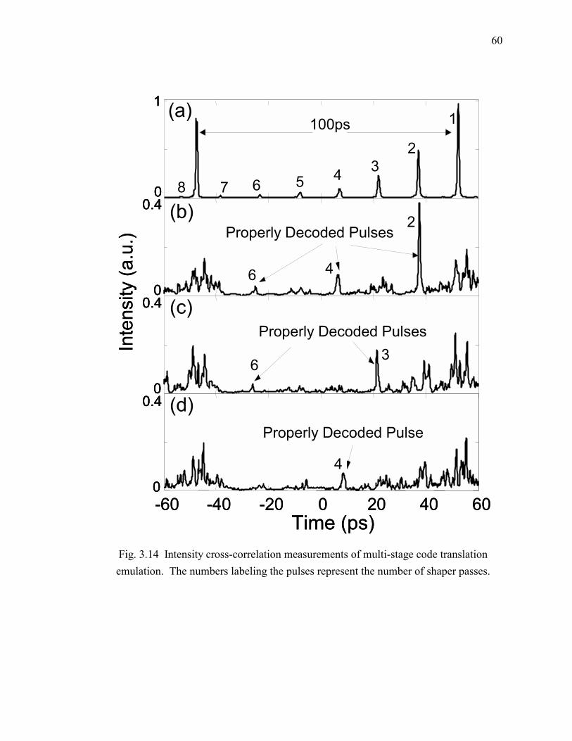
60
-60 -40 -20 0 20 40 60Time (ps)
(a)
Properly Decoded Pulses
Properly Decoded Pulses
Properly Decoded Pulse
1
4
2 3
7 5 6
(b)
(c)
(d)
2
4 6
3 6
4
100ps
8
1
00.4
00.4
00.4
0
Inte
nsity
(a.u
.)
-60 -40 -20 0 20 40 60Time (ps)
(a)
Properly Decoded Pulses
Properly Decoded Pulses
Properly Decoded Pulse
1
4
2 3
7 5 6
(b)
(c)
(d)
2
4 6
3 6
4
100ps
8
1
00.4
00.4
00.4
0
1
00.4
00.4
00.4
0
Inte
nsity
(a.u
.)
Fig. 3.14 Intensity cross-correlation measurements of multi-stage code translation emulation. The numbers labeling the pulses represent the number of shaper passes.

61
4. OPTICAL FIBER TRANSMISSION in O-CDMA SYSTEM In this chapter, we describe 50 km single mode fiber transmission experients in our
O-CDMA testbed [76].
4.1 Pulse Distortion by Fiber Dispersion One of the most significant advantages in optical communication is the capability
of long distance transmission due to two key enabling technologies: (1) low loss transmission media � optical fibers; (2) optical amplification without expensive O/E/O (optical-electrical-optical) regeneration.
Currently, commercial optical fibers have been fabricated to achieve loss performance as low as ~0.2 dB/km within 1.3~1.5 µm wavelength window. For single span transmission without regeneration, ~100 km (20 dB loss) can be routinely implemented. On the other hand, the advent of optical amplifiers, especially Erbium doped fiber amplifiers (EDFA), also radically changed the picture of optical fiber communications. The characteristics making EDFA ideal for optical fiber communication include its large bandwidth, low noise figure, high output power, et. c. With the help of optical amplifiers, more than thousands kilometers fiber transmission has been realized in many commercialized fiber links, which include transoceanic system crossing the Atlantic and the Pacific.
However, in order to transmit O-CDMA signals using optical fibers, there are new challenges. One of these challenges is signal degradation caused by fiber dispersion. Considering a simple fiber transmission model, at fiber input the Fourier transform of optical field is A(ω). After fiber transmission, output optical field is described as A(ω)exp(-iβ(ω)L), where L is fiber length, β(ω) is propagation coefficient,
2 3320 1 0 0 0( ) ( ) ( ) ( )
2 6βββ ω β β ω ω ω ω ω ω= + − + − + − +L (4.1)
where ω0 is carrier frequency. In eq. (1), β0 introduces constant phase shift (relate to phase velocity) and β1 introduces fixed delay (relate to group velocity), which have no effect on pulse broadening or distortion. β2 introduces quadratic frequency dependent phase shift, corresponding to first order dispersion effect, which results in pulse

62
broadening. β3 introduces cubic frequency dependent phase shift, corresponding to second order dispersion effect, which results in pulse distortion (oscillated tails). Fiber dispersion has already been extensively addressed in traditional fiber communication systems and more than thousands of kilometers fiber transmission have been demonstrated. In contrast, O-CDMA signals will be degraded more significantly by fiber dispersion because O-CDMA signals always occupy relatively large optical bandwidth. As a simple estimation, considering the first order dispersion effect, the most widely used single mode fiber (SMF) has a fiber dispersion value 17 ps/nm/km, which will broaden our ~400 fs short pulse (assume 5 nm bandwidth) to 17×5×1=85 ps after even only 1 km fiber transmission, which is more than 200 time of original ~400 fs pulse. It is clear that after fiber transmission properly decoded signal can not be correctly discriminated from improperly decoded noise waveform because of this huge broadening effect.
The most successful and commercialized dispersion compensation (DC) technique is the use of dispersion compensating fiber (DCF) specially designed to have opposite dispersion parameters compared to single mode fiber (SMF), in which most second-order and partial third-order dispersion are compensated. For ultrashort pulses, accumulated residual second- and third-order dispersion in a fiber link can still cause serious distortion even if high quality DCF is used. One solution is to design fiber links with special fiber characteristics and trim the fiber length precisely to match dispersion and minimize distortion. For example, a dispersion slope compensation fiber has been used in a 120-km fiber link to reduce the third-order dispersion for 400-fs pulses [77]. Nonetheless, this technique required special fiber links with very precise trimming of fiber lengths. More seriously, the pulse is still broadened significantly (to 700 fs) because complete DC is extremely difficult if not impossible. A technique for fine tuning of higher order dispersion based on synchronous phase modulation of a pre-chirped pulse has been demonstrated in a 380 fs, 70 km transmission experiment [78]. However, this synchronous modulation scheme restricts the transmission format. Here we discuss a passive, format independent technique capable of fine tuning and completely removing the residual dispersion for a nearly compensated fiber link, which relaxes the required precision in fiber lengths and increases the tolerance to fiber dispersion variations. Previously, our group has demonstrated almost exact third-order correction for 500-fs pulse distortion-free transmission over 2.5 km [79] and 10 km [80] SMF/DCF links using a programmable pulse shaper. The pulse shaper, originally developed for ultrafast optics applications, functions as an adjustable spectral phase equalizer allowing programmable

63
dispersion compensation and reduces the need for careful DCF selection and precise fiber length trimming. In this paper, we extend the capability of this pulse shaping technique applied to fiber dispersion compensation, and report essentially distortion-free transmission for ~500 fs pulses over a 50 km fiber link. The fiber link is a commercial fiber module (directly from the vendor) without extra effort to further control fiber length to minimize residual dispersion. Our results demonstrate that the pulse shaping technique can effectively remove both the residual second- and third-order dispersion for femtosecond pulse transmission in excess of 50 km without strict requirements on the DCF length, which covers the distance range of practical interest for local area network (LAN) and metro area network (MAN) applications using O-TDM or O-CDMA. We also observe the polarization mode dispersion (PMD) effect, which usually plays a role only in long-haul fiber transmission systems. 4.2 Fully Dispersion Compensated ~500 fs Pulse Transmission Over 50 km SMF Fig. 4.1 shows a schematic diagram of our experimental apparatus. An actively mode-locked fiber laser followed by a dispersion decreasing fiber soliton compressor producing nearly transform-limited 400 fs pulses at 10 GHz centered near 1542 nm is used as the pulse source. These ultrashort pulses are input into a fiber coupled Fourier-Transform pulse shaper, which incorporates a 128-element liquid crystal modulator array to apply the spectral phase. This allows dispersion control through the relation
( )( ) ωτ ωω
∂Ψ= −∂
, where ( )τ ω and ( )ωΨ are the frequency-dependent delay and spectral
phase, respectively. The fiber-to-fiber insertion loss of the pulse shaper is less than 5 dB. The output of the pulse shaper is connected to SMF (50.164 km) and DCF modules (OFS Fitel). Total loss for the SMF/DCF link is 14.4 dB. An Erbium doped fiber amplifier (EDFA) is used for loss compensation of the whole system. In our system, most second-order and partial third-order dispersion are compensated by the DCF. The pulse shaper is used for finely tuning dispersion � here we used it in a pre-compensation configuration.
Fig. 4.2 shows the intensity cross-correlation measurement where the reference arm is a 400 fs pulse directly from the laser. The pulse is first measured without the SMF/DCF modules (dashed curve) showing a pulse broadened to 460 fs (FWHM) primarily due to the EDFA gain profile and slight spectral filtering in the pulse shaper. When the 50 km SMF/DCF module is inserted we can fine tune the phase profile of the pulse shaper to compensate residual second- and third-order dispersion, and can recover a 470 fs pulse (solid curve), which dramatically demonstrates the capability of essentially

64
complete dispersion compensation for sub-500 fs short pulses over 50 km of SMF by combining the techniques of DCF and a pulse shaper. Fig. 4.3 shows the details of the fine DC using the pulse shaper. After the SMF alone, the calculated pulse broadening (not shown) is ~5 ns! After the SMF/DCF modules, although most second-order and partial third-order dispersion is compensated, the pulse is still significantly distorted and broadened to 13.9 ps (dotted curve). If we program the pulse shaper to compensate the residual second-order dispersion only, the pulse shows an oscillating tail (dashed curve) indicative of residual third-order dispersion. If we program the pulse shaper to compensate both residual second- and third-order dispersion, the pulse is recovered back to 470 fs (solid curve). The inset figure shows the quadratic and cubic phase profile applied by the pulse shaper to cancel the residual second- and third-order dispersion. Please note that the phase is actually applied to the pulse shaper modulo 2π, which significantly extends the dispersion compensation range.
We emphasize that in our results above, the fiber link is a commercial fiber module (directly from the vendor) without extra effort to further control fiber length to minimize residual dispersion. Based on the spectral phase applied by the pulse shaper, we can calculate the residual dispersion of the SMF/DCF modules. Accordingly, we insert an additional 120 m of SMF to fully compensate the calculated residual second-order dispersion. Fig. 4.4 shows the intensity cross-correlation measurement (dashed curve), which is still broadened with an oscillating tail caused by residual third-order dispersion. The main point is that even high quality DCF and precise fiber length control will still result in significant pulse broadening and distortion for such short pulses after fiber transmission. After applying pure cubic spectral phase for third-order dispersion compensation in the pulse shaper, the short pulse is recovered (solid curve). The inset figure shows the pure cubic spectral phase profile applied in the pulse shaper.
In our system, essentially complete second- and third-order dispersion compensation is the key to achieve 50 km SMF transmission for sub-500 fs pulses. The input power to the fiber link is 8.7 dBm, corresponding to 740 fJ per pulse at 10 GHz. At this power the primary nonlinear effect, self-phase modulation, is not an important factor because of fiber loss and the rapid pulse broadening in the fibers [81]. However, polarization mode dispersion (PMD) [82,83] starts to appear in our system because of the large bandwidth inherent in the short pulse. To check the effect of PMD, optical spectra are examined through a polarization controller (PC) and linear polarizer for different PC settings. Fig. 4.5 (A) shows the spectra without the 50 km fiber transmission demonstrating no variation across the spectra for different PC settings. Fig. 4.5 (B)

65
shows several spectra out of the 50 km fiber link for different PC settings. The variation of the spectral profiles as a function of polarization component is a clear sign of PMD. In the measurement shown in Fig. 4.2-4.4, degradation due to PMD was mitigated by coupling the input short pulse into one principal state of polarization (PSP) of the fiber link. Fig. 4.5 (C) shows the intensity auto-correlation traces out of the 50 km fiber link for different input polarization states at the fiber link input. The minimum pulse width can be achieved by tuning the input polarization to either of the two PSPs, as shown by the solid and dashed curves. When a non-PSP state is launched, the pulse is broadened to 600 fs (dotted curve). PMD could be a limiting factor in extending the transmission distance further for such short pulses. Finally, note that pulse shaper works as desired only if the phase shift per pixel is sufficiently below π. This imposes a time aperture limit - the broadening that is to be compensated (13.9 ps in our experiment) should remain safely below the inverse of the frequency bandwidth per pixel (~60 ps for the current pulse shaper). This limit can be further relaxed by pulse shaper design. 4.3 50 km SMF Fiber Transmission for O-CDMA
Now we integrate the fiber transmission technique into our O-CDMA testbed. In our O-CDMA testbed, the spectral phase encoding/decoding is also implemented by the pulse shaper. As a result, we can combine the function of dispersion compensation to either the encoder or decoder to simplify system implementation. In O-CDMA, multiple-access is achieved by assigning different, minimally interfering code sequences to different CDMA transmitters. In our spectrally phase coded O-CDMA system, input ultrashort pulses are time-spread during the encoding process into lower intensity noise-like signals. In the receiver, data corresponding to a desired user are separated from multi-access interference (MAI) via decoding operation, in which properly decoded signals are converted back to the original pulse-like signals, while improperly decoded signals remain low-intensity noise-like temporally broadened waveforms. Fig. 4.6 shows the intensity cross-correlation measurement after 50 km fiber transmission in a 2-user O-CDMA system. For the desired user, the link output is properly decoded back to a short pulse after 50 km SMF transmission, which demonstrates both the successful encoding/decoding process and full dispersion compensation. Compared with the uncoded pulses, also after a transmission through 50 km of fiber, shown in Fig. 4.2-4.4, the properly decoded short pulse is somewhat degraded exhibiting side-lobes and a pedestal, which are caused by the encoding/decoding process. The interference user is

66
improperly decoded to a noise-like waveform. To reject the interference user, we use a highly sensitive fiber pigtailed periodically-poled lithium niobate (PPLN) waveguide to perform the nonlinear discrimination function based on second harmonic generation (SHG). Fig. 4.7 shows the O-CDMA system performance (eye diagrams and bit error rate BER), where a 2.5 Gb/s PRBS 223-1 data stream is impressed on the ~400 fs, 10 GHz mode-locked fiber laser output and then split to generate both desired and interference user. For both single-user and two users, the power penalty at BER=10-9 caused by 50 km fiber transmission is less than 1.3 dB.

67
10GHz ~400fs Pulse
50 km SMF DCF
Programmable pulse shaper EDFA
Measurement
10GHz ~400fs Pulse
50 km SMF DCF
Programmable pulse shaper EDFA
Measurement
Fig. 4.1. Experimental apparatus.
-10 -5 0 5 10Time (ps)
Inte
nsity
cro
ss-c
orre
latio
n (a
.u.)
with 50 km fiber, 470 fsw/o 50 km fiber, 460 fs
-10 -5 0 5 10Time (ps)
Inte
nsity
cro
ss-c
orre
latio
n (a
.u.)
with 50 km fiber, 470 fsw/o 50 km fiber, 460 fs
Fig. 4.2. Intensity cross-correlation with and without SMF/DCF module, demonstrating
distortionless 50 km fiber transmission for sub-500 fs pulses.

68
-10 -5 0 5 10 15 20Time (ps)
Inte
nsity
cro
ss-c
orre
latio
n (a
.u.)
both second- and third-order DC by pulse shaper
without DC by pulse shapersecond-order DC by pulse shaper
0 64 128
50
100
Pixel #
App
lied
spec
tral p
hase
by p
ulse
sha
per
(rad)
-10 -5 0 5 10 15 20Time (ps)
Inte
nsity
cro
ss-c
orre
latio
n (a
.u.)
both second- and third-order DC by pulse shaper
without DC by pulse shapersecond-order DC by pulse shaper
0 64 128
50
100
Pixel #
App
lied
spec
tral p
hase
by p
ulse
sha
per
(rad)
0 64 128
50
100
Pixel #
App
lied
spec
tral p
hase
by p
ulse
sha
per
(rad)
Fig. 4.3. Intensity cross-correlation for different pulse shaper settings. The inset figure
shows an unwrapped version of the phase profile applied by the pulse shaper. The actual phase profile that is applied is modulo 2π.
-10 -5 0 5 10 15 20Time (ps)
Inte
nsity
cro
ss-c
orre
latio
n (a
.u.)
pure third-order DC by pulse shaper
without DC by pulse shaper
0 64 128-30
0
30
Pixel #
App
lied
spec
tral p
hase
by p
ulse
sha
per
(rad)
second-order DC by inserting 120 m SMF
-10 -5 0 5 10 15 20Time (ps)
Inte
nsity
cro
ss-c
orre
latio
n (a
.u.)
pure third-order DC by pulse shaper
without DC by pulse shaper
0 64 128-30
0
30
Pixel #
App
lied
spec
tral p
hase
by p
ulse
sha
per
(rad)
0 64 128-30
0
30
Pixel #
App
lied
spec
tral p
hase
by p
ulse
sha
per
(rad)
second-order DC by inserting 120 m SMF
Fig. 4.4. Intensity cross-correlation for different pulse shaper settings by inserting an
additional 120 m SMF for complete second-order DC. The inset figure shows the unwrapped phase profile applied by the pulse shaper (again the actual phase is applied
modulo 2π).
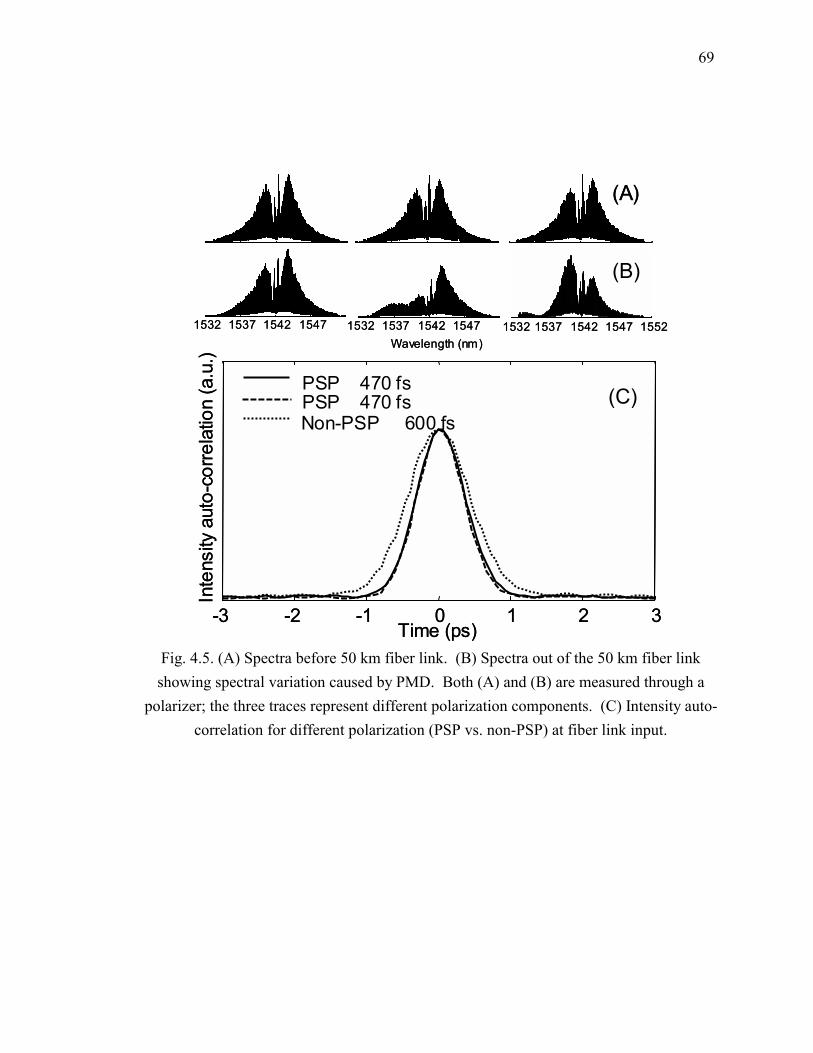
69
-3 -2 -1 0 1 2 3Time (ps)
Inte
nsity
aut
o-co
rrela
tion
(a.u
.)
Non-PSP 600 fs
PSP 470 fsPSP 470 fs
1532 1537 1542 1547Wavelength (nm)
1532 1537 1542 1547 1532 1537 1542 1547 1552
(C)
(B)
(A)
-3 -2 -1 0 1 2 3Time (ps)
Inte
nsity
aut
o-co
rrela
tion
(a.u
.)
Non-PSP 600 fs
PSP 470 fsPSP 470 fs
1532 1537 1542 1547Wavelength (nm)
1532 1537 1542 1547 1532 1537 1542 1547 1552
(C)
(B)
(A)
Fig. 4.5. (A) Spectra before 50 km fiber link. (B) Spectra out of the 50 km fiber link showing spectral variation caused by PMD. Both (A) and (B) are measured through a
polarizer; the three traces represent different polarization components. (C) Intensity auto-correlation for different polarization (PSP vs. non-PSP) at fiber link input.

70
-50 0 50Time (ps)
Desired user
Interference user
Inte
nsity
cro
ss-c
orre
latio
n (a
.u.)
-50 0 50Time (ps)
Desired user
Interference user
-50 0 50Time (ps)
Desired user
Interference user
Inte
nsity
cro
ss-c
orre
latio
n (a
.u.)
Fig. 4.6. Intensity cross-correlation for a 2 user O-CDMA system after 50 km fiber
transmission.
-6 -4 -2 0 2 4 6 8Total Power to PPLN (dBm)
1e-10
BER
1e-11
1e-9
1e-8
1e-7
1e-6
1e-5
1e-41 user, w/o 50 km fiber1 user, with 50 km fiber2 users, w/o 50 km fiber2 users, with 50 km fiber
2 users, w/o 50 km fiber
2 users, with 50 km fiber
-6 -4 -2 0 2 4 6 8Total Power to PPLN (dBm)
1e-10
BER
1e-11
1e-9
1e-8
1e-7
1e-6
1e-5
1e-4
1e-10
BER
1e-11
1e-9
1e-8
1e-7
1e-6
1e-5
1e-41 user, w/o 50 km fiber1 user, with 50 km fiber2 users, w/o 50 km fiber2 users, with 50 km fiber
1 user, w/o 50 km fiber1 user, with 50 km fiber2 users, w/o 50 km fiber2 users, with 50 km fiber
2 users, w/o 50 km fiber
2 users, with 50 km fiber
Fig. 4.7. BER performance for the O-CDMA system with and without 50 km fiber
transmission. The inset figures show the eye diagrams for 2 users.

71
5. SECURITY ISSUES in O-CDMA SYSTEM In this chapter we investigate the security issues in O-CDMA system [84,85].
5.1 Security Issues The potential provided by O-CDMA for enhanced information security is
frequently mentioned in addition to other possible advantages, such as simplified and decentralized network control, improved spectral efficiency, and increased flexibility in the granularity of bandwidth that can be provisioned. This is plausible at first glance considering that frequently the O-CDMA encoded signal manifests itself as a noise-like waveform that may not be accessible to an eavesdropper without knowledge of the applied code. Therefore, for a properly configured system, an eavesdropper may potentially experience a significant disadvantage in signal to noise ratio compared to the authorized O-CDMA receiver. However, this argument is worth deeper consideration. Our group has previously demonstrated there is no security at all in spectrally phase-coded O-CDMA for a single-user system employing on-off keying (OOK) as shown in Fig. 2.9(B) in chapter 2. This is due to the fact that for an OOK system, although the encoded waveform is noise-like on an ultrafast time scale, it can be detected using a simple energy detector without any knowledge of the spectral code. For example, the energy detector could be a standard receiver bandwidth-limited to the bit rate which is unable to resolve the fine structure of the noise-like waveforms but integrates the energy in a bit period. As a result, although on an ultra-fast time scale the noise-like coded waveform is very different from the properly decoded short pulses, it still shows a clear eye-diagram, which could be detected by an eavesdropper with no knowledge of the code. Therefore, there is no security at all for such OOK single user O-CDMA systems. On the other hand, even in a multi-user network environment, there are typically still fiber links where only a single user exists (for example, the upstream traffic in a star network as shown in Fig. 5.1, as pointed out by a recent systematic theoretical study on security issues in O-CDMA [86,87]. In this case eavesdropping can be easily accomplished using a simple energy detector if an on-off keying data modulation format is used, as pointed out above. References [86,87] suggest that the vulnerability to eavesdropping can be reduced for a data modulation format based on switching between two code words (in the

72
following we refer to this as code switching or two-code keying). It is also suggested that spectral phase coding is one of the more promising approaches for O-CDMA from a security perspective, due to the large code space.
The theoretical study in [86,87] concentrates on paths with isolated single users, which are the most vulnerable and analyzes the probability that the eavesdropper can fully and precisely determine the O-CDMA code. Specific eavesdropping detector structures are presented to illustrate the possibility of the eavesdropper breaking the security of spectral phase coded signals by directly measuring the code words. The proposed hardware approach for eavesdropping is quite complex from the practical implementation perspective but in principle should be possible. The analysis shows that the probability of full code determination depends on the signal-to-noise ratio considering the energy at the eavesdropper per chip (as opposed to the full energy integrated over the spectral code). References [86,87] also show that the probability of full code interception increases rapidly if the eavesdropper is able to integrate measurement results over multiple repetitions of the code word (i.e., over multiple data bits), but point out that such integration will likely be precluded for a two-code-keying spectrally phase coded O-CDMA system.
In our laboratory we implement a code-switching scheme for spectrally phase coded O-CDMA experimentally. Our experiments demonstrate that the code switching data modulation format enhances security compared to on-off keying by eliminating the vulnerability to eavesdropping based on a simple energy detector, as suggested in [86,87]. We also investigate and experimentally demonstrate simple vulnerabilities, not previously reported, that allow eavesdropping of data from an isolated user on a two-code-keying spectrally phase coded O-CDMA system. These vulnerabilities allow data recovery with simple hardware and without the need for any attempt to learn the code.
5.2 Code Switching Scheme
A schematic diagram of the code-switching scheme is shown in Fig. 5.2. An actively mode-locked fiber laser (~3 ps) followed by a dispersion decreasing fiber soliton compressor producing nearly transform-limited ~0.4 ps pulses at 10 GHz repetition rate centered near 1542 nm is used as the pulse source. A coupler is used to generate two arms in a complementary modulator geometry to achieve code-switching. Each arm is equipped with an intensity modulator employing OOK and driven by the same 10 Gb/s PRBS 231-1 data stream, but data and data bar are assigned to the two arms respectively. The data modulated ultrashort pulses are input into fiber coupled Fourier Transform pulse

73
shapers which incorporate 128 element liquid crystal modulator arrays to spectrally phase code the spectrum of the source laser. Two different codes (here length 31 M-sequence codes) are applied to the two arms to realize code switching. In order to achieve high quality code-switching, care is taken to match the average power and fiber length in each arm. After combining the two arms, bit �1� and �0� are occupied by two distinct but equal energy noise-like waveforms encoded according to code 1 and code 2, respectively. An additional pulse shaper can be used as a post-processing coder to enhance the security as will be discussed later. The receiver consists of a pulse shaper used to decode the authorized user, a highly sensitive fiber pigtailed periodically-poled lithium niobate (PPLN) waveguide chip to perform the second harmonic generation (SHG) nonlinear discrimination function, and a photo-diode operating at the SHG wavelength of 0.77 µm adapted from 10 Gb/s Ethernet. This is the same receiver structure we used in our previous O-CDMA studies employing on-off keying. For two-code-keying operation, this ideally converts one of the desired transmitter codes to a high output level, while converting the second code from the desired transmitter as well as any O-CDMA multi-access interference signals to a low output level. In principle, a two-code-keying receiver consisting of a splitter and a pair of parallel decoders (matched to the two respective transmit waveforms) and SHG chips, followed by a differencing operation, might offer more optimal performance, but this was not implemented in our experiments. For the purposes of this demonstration it is assumed that an eavesdropper could tap into the fiber link somewhere after the complementary modulator (and post-processing coder) but before the decoder.
For an eavesdropper using an energy detector (here a 20 GHz bandwidth photo-diode at 1.5 µm), the eye-diagram is clear for a single arm (traditional single user O-CDMA) and as discussed there is no security at all. But for the code-switching scheme, there is no eye-diagram at all with such a simple energy detector since both bit �1� and �0� are occupied by encoded waveforms. In this sense the security is enhanced since the information is concealed by the code-switching scheme to resist simple interception from a malicious eavesdropper. Fig. 5.3(a) shows the uncoded spectrum and corresponding intensity cross-correlation measurement, which is ~400 fs short pulse. Figs. 5.3(b) and (c) show the coded spectra of the two arms in the code-switching scheme, which are measured individually by blocking the opposite arm. The short pulses are broadened to noise-like waveforms after encoding. Although noise-like waveforms are distinct from each other between two arms on an ultrafast time scale due to different codes, an energy detector, which could be a standard receiver bandwidth-limited to the bit rate, is unable to
74
resolve the fine structure of the noise-like waveforms but integrates the energy in a bit period. As a result, bit �1� and �0� represented by these two waveforms from two arms cannot be distinguished using such a detector. Fig. 5.3 (d) shows the time-domain waveform of the combined signals detected by the photo-diode and measured by a sampling scope, which confirms that there is no eye-diagram in the code-switching scheme.
Our experiments demonstrate that the code switching data modulation format enhances security compared to on-off keying by eliminating the vulnerability to eavesdropping based on a simple energy detector, as suggested in [86,87]. We noted, however, that this did not preclude the possibility of vulnerability to eavesdropping strategies that exploit other structure in the coding and signaling scheme. In the following sections, we investigate and experimentally demonstrate simple vulnerabilities, not previously reported, that allow eavesdropping of data from an isolated user on a two-code-keying spectrally phase coded O-CDMA system. These vulnerabilities allow data recovery with simple hardware and without the need for any attempt to learn the code. 5.3 Vulnerability From Coding Induced Spectral Dips
However, for the spectrally phase coded O-CDMA investigated by several groups including our own, the coding process will generate spectral dips as shown in Fig. 5.3 (a) and (b). This phenomenon results from diffraction effects experienced by frequency components falling at transitions in the spectral phase code [60]. This effect is not due to practical imperfections; it is expected for fundamental reasons and has been explained quantitatively in [60]. In the spectral phase coding process, the frequency components of each chip are phase shifted by 0 or π according to the length-31 M-sequence codes. Therefore, each spectral dip marks a phase transition. From the measured spectral data, one can easily recover the codes according to this principle. Other (relatively complicated) methods have also proposed for an eavesdropper to measure the code [86,87]. Here we show that the spectral dips lead to structure in the signals that can be exploited directly for eavesdropping in a simple way. For the code-switching scheme, clear spectral measurements for individual arms become somewhat difficult since two differently coded spectra are combined together. However, one can recover the data by simply scanning a narrow bandpass optical filter across the combined spectra even without measuring the code. At the spectral positions where one arm has a dip while the other arm does not, there is a power difference between them. Such power difference will generate eye-diagrams, which is similar to an OOK signal from a single arm. Fig. 5.4

75
shows such an example. In the vicinity of 1542 nm there is no dip for arm 1 but a dip for arm 2 on the coded spectra as shown in Fig. 5.4(a) and (b). We use a high resolution pulse shaper (please refer to chapter 6) as a tunable narrow bandpass filter to achieve this discrimination, where 4 spectral lines (separated at 10 GHz � the repetition rate) are filtered out. As expected, an eye-diagram shown in Fig. 5.4 (c) is observed, which demonstrates a very clear vulnerability to eavesdropping.
Since there are multiple spectral dips in the spectra, the eavesdropper may scan the narrow bandpass optical filter across the spectra to locate the position to detect the data. Fig. 5.5 shows such typical measurements at those possible positions of spectral dips (at the edge of each code chip), where there is (a) dip for arm 1 but no dip for arm 2, (b) dips for both arms and (c) no dips for both arms, respectively. Similarly to Fig. 5.4, Fig. 5.5(a) shows an eye-diagram demonstrating a clear vulnerability. As expected, there are no eye-diagrams for (b) and (c). For an eavesdropper without knowledge of the code, generally there are many locations across the spectra to detect the data. For example, assuming the phase shift (0 or π) for each code chip is randomly assigned, there is 50% probability to detect data with clear eye-diagram for each possible position of spectral dips. As a result, half of those positions are vulnerable to eavesdropping.
The bandwidth of the narrow bandpass optical filter also plays an important role in the eavesdropping capability. In this particular example, a bandwidth allowing 4 spectral lines to pass through is appropriate to measure a clear eye-diagram. For comparison, we change the bandwidth to allow 8 spectral lines and 20 spectral lines pass through, respectively, as shown in Fig. 5.6. The power difference between the two arms within the bandwidth corresponding to 8 spectral lines still permits measuring an eye-diagram in Fig. 5.6(a). However, the power difference between two arms becomes smaller relative to the total power as the bandwidth increases, showing almost no eye-diagram for the 20 spectral line case, Fig. 5.6(b). This illustrates that the optimal parameters for the eavesdropper depend highly on the details of O-CDMA system configuration. The performance of the eavesdropper will depend on the received energy per spectral chip relative to the noise level, which also depends on the O-CDMA system parameters. It should also be noted one can easily envision strategies that will improve eavesdropping performance by combining the energy from multiple spectral dip locations.
One simple strategy to improve security in terms of concealing the structure of spectral dips is to intentionally generate spectral dips at all possible positions (at the edge of each code chip). For this purpose, an additional pulse shaper is used as a post-processing coder right after the complementary modulator. Figs. 5.7 (a) and (b) show the
76
spectra of the individual arms after the post-processing coder, where spectral dips appear at all possible positions. Fig. 5.7 (c) shows the waveform (no eye-diagram), which is similar to Fig. 5.3(c). The post-processing coder is operated such that phase shifts of 0 and π are applied alternatively to alternating code chips. Such phase transitions generate spectral dips at all spectral positions independent of code. Now, the eye-diagram is well concealed even using a narrow bandpass filter, as shown in Fig. 5.8. On the other hand, it is important to show that the code-switching scheme with post-processing (spectral dips everywhere) still works for the authorized user using conventional O-CDMA detection: decoded by a decoder, discriminated by the PPLN, and detected by the photo-diode at 0.77 µm. Fig. 5.9 shows the eye-diagram for single arm (a), for code-switching (both arms) (b) and for code-switching with post-processing (c), where arm 1 is properly decoded. The clear eye-diagrams and bit-error-rate measurement in Fig. 5.9 demonstrate the code-switching scheme with post-processing still works for the authorized user using conventional O-CDMA detection. Note that for the code-switching scheme with post-processing (Fig. 5.9(c)), to correctly decode arm 1, the spectral phase of the decoder is set to compensate the sum of the spectral phases from the arm 1 encoder and the post-processing coder. This is similar to code translation in spectrally phase coded O-CDMA described in chapter 3. The ~3 dB power penalty between curves (a) and (b) is expected, since ideally SHG is generated only for code 1, while codes 1 and 2 are both present at the SHG chip at equal power level. The additional small power penalty due to post-processing, around 0.6 dB, is explained on the basis of small changes in the properly decoded pulses as a result of extra spectral dips inserted by the post-processing coder. 5.4 Vulnerability From a DPSK Demodulator
In the code-switching scheme, bit �1� and �0� are occupied by different spectrally phase coded waveforms. This is analogous to binary phase shift keying (BPSK), where each bit has constant energy but is data-coded with 0 or π phase shift for bit �0� or �1�. Therefore, a simple differential phase shift keying (DPSK) demodulator can also be used to recover data from the code-switching scheme. The DPSK format has been intensely investigated in optical fiber communication systems in recent years [88]. Briefly, the DPSK demodulator is a one-bit-delay interferometer, in which the incoming signal is split into two paths and combined again with one-bit difference between the two paths. In conventional BPSK/DPSK the signals add constructively at the interferometer output for like adjacent bits (�00� or �ππ�) and destructively for unlike adjacent bits (�0π� or �π0�). This converts the phase modulation into an intensity contrast. DPSK

77
demodulation of two-code-keyed O-CDMA signals works in a similar way, provided that the interferometer delay is carefully matched to the data rate with precision better than the coherence time of the O-CDMA signal (usually this is the duration of the original mode-locked pulse). When adjacent bits are identical (same code waveforms), they can interfere constructively to give a high output. However, when adjacent bits correspond to different code waveforms, their interference is close to zero due to averaging over different spectral chips (assuming the usual case of code pairs with low cross-correlation).
Here we use a DPSK demodulator scheme which is based on polarization maintaining (PM) fiber [89], as shown in Fig. 5.10. Light is launched at 45º to the principle axes of the 86.3 meter length of PM fiber, which provides a 120.5 ps delay difference for light traveling along the fast and slow axes. To match the bit rate of the DPSK demodulator, the mode-locked laser is set to 8.3 GHz repetition rate. Phase differences between adjacent bits lead to polarization changes at the output of the PM fiber, which are converted to an intensity contrast after the polarizer. In an ideal DPSK receiver the power of both polarization states separated by the polarizer would be measured and subtracted. For simplicity in our experiment we measured only the light transmitted through the polarizer, which is already sufficient to demonstrate eavesdropping.
We use 3 ps pulses directly from the mode-locked laser as the input to the code-switching modulator in our DPSK experiment. The O-CDMA code-switching signal processed by the DPSK demodulator and then detected by the photo-diode is shown in Fig. 5.11(a). An eye-diagram is apparent although it is noisy. The noise comes from frequency fluctuations in the mode-locked laser frequency comb as well as lack of stabilization of the interferometer. We note that the requirement of good frequency stability (narrow linewidth) of the source laser in conventional coherent optical communication is translated into a requirement that the mode-locked laser have a frequency comb with good absolute frequency stability (narrow linewidth) for each of the comb lines. A recent high resolution pulse shaping experiment showed that frequency fluctuations in a mode-locked frequency comb lead to intensity fluctuations when the pulse shaper output depends on interferometric addition of contributions from adjacent mode-locked pulses [50]. A similar effect occurs in our DPSK measurement and contributes to the noisy eye. Nevertheless, the presence of an eye immediately demonstrates a clear vulnerability to eavesdropping. Fig. 5.11(b) selects several scans of the waveforms with clear eyes, to emphasize the possibility of such vulnerability.

78
The DPSK vulnerability identified above is a very serious one for several reasons. First, the eavesdropping scheme does not require any attempt to learn the O-CDMA code. Second, the eavesdropper is unaffected if the code pair used in the code-switching modulator is changed. Third, the eavesdropper is able to exploit the full energy in the intercepted signal, as opposed to other schemes where only the energy per code chip can be exploited [86,87]. Given that the eavesdropper is able to use a conventional high sensitivity detector requiring only a few femtojoules per bit, while the O-CDMA receiver requires nonlinear processing (demonstrated down to 30 fJ per bit, which is still an order of magnitude higher than conventional lightwave receivers), there is a significant likelihood that the eavesdropper can attain signal-to-noise ratio comparable to or even better than that of the O-CDMA receiver. Clearly, this fails to fulfill the premise for security in O-CDMA, which is that the eavesdropper without knowledge of the code should be at a signal-to-noise ratio disadvantage. It is important therefore to attempt to identify means by which the transmitter can mask single-user, two-code-keyed O-CDMA data from a DPSK receiver. This could be a subject of future work.
5.5 Conclusion
The code switching data modulation format enhances security in O-CDMA compared to on-off keying by eliminating the vulnerability to eavesdropping based on a simple energy detector. Nevertheless, in this paper we have experimentally demonstrated two vulnerabilities for such a code-switching scheme that allow eavesdropping of data from an isolated user in a two-code-keying spectrally phase coded O-CDMA system. These vulnerabilities exploit structure in the coding and signaling schemes to recover data, with relatively simple hardware and without requiring knowledge of the codes. We have also demonstrated a modified coding scheme that mitigates one of the eavesdropping vulnerabilities. A key conclusion of our work is that there may be many opportunities for exploiting structure in coded O-CDMA signals in order to eavesdrop, without the need to measure and determine the code. Although we have focused our investigation on spectral phase coding with an isolated user, it is likely that other O-CDMA schemes suffer from analogous vulnerabilities based on their structure. It may also be possible to extend these ideas to extract data in cases where traffic from multiple O-CDMA users is superimposed. Therefore, one needs to exercise great care in assessing and mitigating such vulnerabilities if the security features of O-CDMA are of interest.
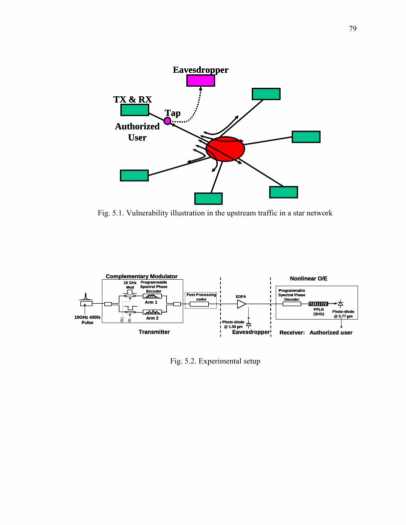
79
Eavesdropper
Authorized User
TapTX & RX
Eavesdropper
Authorized User
TapTX & RX
Fig. 5.1. Vulnerability illustration in the upstream traffic in a star network
Complementary Modulator
Photo-diode @ 0.77 µµµµm
PPLN (SHG)
10GHz 400fs Pulse
Programmable Spectral Phase
Encoder Programmable Spectral Phase
DecoderEDFA
10 GHzMod
Nonlinear O/E
Eavesdropper Receiver: Authorized user
Photo-diode @ 1.55 µµµµm
Arm 1
Arm 2
Post-Processing coder
Transmitter
Complementary Modulator
Photo-diode @ 0.77 µµµµm
PPLN (SHG)
10GHz 400fs Pulse
Programmable Spectral Phase
Encoder Programmable Spectral Phase
DecoderEDFA
10 GHzMod
Nonlinear O/E
Eavesdropper Receiver: Authorized user
Photo-diode @ 1.55 µµµµm
Arm 1
Arm 2
Post-Processing coder
Transmitter
Fig. 5.2. Experimental setup

80
(b) Arm 1
1535 1540 1545 1550Wavelength (nm)
(c) Arm 2
(d)
0 50 100 150 200Time (ps)
0 50 100 150 200Time (ps)
Spectral dips
-20 -10 0 10 20Time (ps)
(a) Spectra Intensity cross-correlation
Fig. 5.3. Spectra and corresponding intensity cross-correlation of (a) uncoded , (b) coded
arm 1 and (b) coded arm 2. (d) Waveform of the combined signals measured by photo-
detector and sampling scope.
(a) Arm 1
1541.5 1542 1542.5Wavelength (nm)
(b) Arm 2
(c)
0 50 100 150 200Time (ps)
(a) Arm 1
1541.5 1542 1542.5Wavelength (nm)
(b) Arm 2
(c)
0 50 100 150 200Time (ps)
0 50 100 150 200Time (ps)
Fig. 5.4. Spectra of (a) arm 1 without dip and (b) arm 2 with dip filtered by a narrow
bandpass filter in the vicinity of 1542 nm. (c) Waveforms.
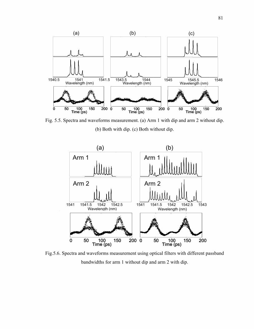
81
1540.5 1541 1541.5Wavelength (nm)
1543.5 1544Wavelength (nm)
1545 1545.5 1546Wavelength (nm)
0 50 100 150 200Time (ps)
0 50 100 150 200Time (ps)
0 50 100 150 200Time (ps)
0 50 100 150 200Time (ps)
0 50 100 150 200Time (ps)
0 50 100 150 200Time (ps)
(a) (b) (c)
Fig. 5.5. Spectra and waveforms measurement. (a) Arm 1 with dip and arm 2 without dip.
(b) Both with dip. (c) Both without dip.
1541 1541.5 1542 1542.5 1543Wavelength (nm)
1541 1541.5 1542 1542.5Wavelength (nm)
Arm 1
Arm 2
Arm 1
Arm 2
0 50 100 150 200Time (ps)
0 50 100 150 200Time (ps)
0 50 100 150 200Time (ps)
0 50 100 150 200Time (ps)
(a) (b)
Fig.5.6. Spectra and waveforms measurement using optical filters with different passband
bandwidths for arm 1 without dip and arm 2 with dip.

82
1535 1540 1545 1550Wavelength (nm)
(a) Arm 1
(b) Arm 2
(c)
0 50 100 150 200Time (ps)
1535 1540 1545 1550Wavelength (nm)
(a) Arm 1
(b) Arm 2
(c)
0 50 100 150 200Time (ps)
Fig. 5.7. Spectra of (a) arm 1 and (b) arm 2 after post-processing. (c) Waveforms.
processing. (c) Waveforms.
1541.5 1542 1542.5Wavelength (nm)
(a) Arm 1
(b) Arm 2
(c)
0 50 100 150 200Time (ps)
1541.5 1542 1542.5Wavelength (nm)
(a) Arm 1
(b) Arm 2
(c)
0 50 100 150 200Time (ps)
0 50 100 150 200Time (ps)
Fig. 5.8. Spectra of (a) arm 1 and (b) arm 2 in the vicinity of 1542 nm after post-
processing. (c) Waveforms.

83
0 50 100 150 200Time (ps)
0 50 100 150 200Time (ps)
0 50 100 150 200Time (ps)
1e-10
Total Power to PPLN (dBm)
BE
R
-6 -4 -2 0 2
1e-9
1e-6
1e-4
1e-5
1e-3
1e-7
1e-8
1e-10
Total Power to PPLN (dBm)
BE
R
-6 -4 -2 0 2
1e-9
1e-6
1e-4
1e-5
1e-3
1e-7
1e-8
(a)
(b)
(c)
(a)(b)(c)
Fig. 5.9. Eye diagrams and BER measurements for authorized user: (a) single arm, (b)
code-switching, (c) code-switching with post-processing.

84
PC 86.3 m PM fiber PC
45o Polarizer
Eavesdropper
Photo-diode @ 1.55 µµµµm
OCDMA Code-Switching Signal
DPSK de-modulator
Fig. 5.10. Experimental setup to investigate vulnerability using a DPSK de-modulator.
PC: polarization controller. PM: polarization maintaining.
(a) (b)
0 50 100 0 50 100Time (ps) Time (ps)
150 200
(a) (b)
0 50 100 0 50 100Time (ps) Time (ps)
150 200
Fig. 5.11. (a) Waveforms after DPSK de-modulator. (b) Picking up several scans of the
waveforms with clear eyes, to emphasize such possible vulnerabilities.

85
6. SPECTRAL LINE-BY-LINE PULSE SHAPING
In this chapter we describe our spectral line-by-line pulse shaping results [50].
6.1 Group Line Pulse Shaping Versus Line-by-Line Pulse Shaping In the frequency domain, mode-locked laser pulses are characterized by a series of
discrete spectral lines (optical frequency comb) with the frequency interval equal to the pulse repetition rate. Spectral lines and their stabilization in mode-locked lasers have recently played a critical role in the progress of optical frequency metrology and optical carrier-envelope phase control [46]. It has been shown that the optical spectral lines (optical frequency comb) for a mode-locked laser can be expressed as [46]
n repf n f ε= + (6.1)
where n is a large integer, frep is frequency interval between two spectral lines (also the repetition rate of mode-locked laser), and ε is the comb-offset frequency. The offset frequency ε is related to the evolution of the carrier-envelope phase, which occurs as the result of a mismatch in the group and phase velocities inside the laser cavity. Adjacent pulses in the mode-locked pulse train have relative phase difference 2πε/frep. Therefore, stable (unstable) offset frequency ε implies fixed (fluctuating) phase relationship between adjacent pulses. If the adjacent pulses can be manipulated in a way such that they overlap with each other, this phase relationship can be observed through their interference.
From the pulse shaping perspective, if it is possible to independently manipulate both the amplitude and phase of individual spectral lines, essentially full pulse shape control can be achieved. Specifically, waveforms formed from adjacent pulses can overlap with each other. However, in typical pulse shapers spectral lines are manipulated in groups rather than individually. This is primarily due to the practical difficulty of building a pulse shaper capable of resolving each spectral line for typical mode-locked lasers with repetition rates below 1 GHz. Group-of-lines pulse shaping is illustrated in Fig. 1.5(A), where frep is the repetition rate defined above. Assuming that the pulse shaping occurs M lines at a time, the shaped pulses have maximum duration ~1/(Mfrep) and repeat with period T=1/frep. Accordingly, the pulses are isolated in time. In contrast,
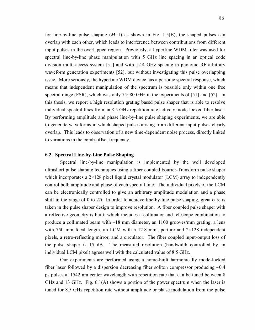
86
for line-by-line pulse shaping (M=1) as shown in Fig. 1.5(B), the shaped pulses can overlap with each other, which leads to interference between contributions from different input pulses in the overlapped region. Previously, a hyperfine WDM filter was used for spectral line-by-line phase manipulation with 5 GHz line spacing in an optical code division multi-access system [51] and with 12.4 GHz spacing in photonic RF arbitrary waveform generation experiments [52], but without investigating this pulse overlapping issue. More seriously, the hyperfine WDM device has a periodic spectral response, which means that independent manipulation of the spectrum is possible only within one free spectral range (FSR), which was only 75~80 GHz in the experiments of [51] and [52]. In this thesis, we report a high resolution grating based pulse shaper that is able to resolve individual spectral lines from an 8.5 GHz repetition rate actively mode-locked fiber laser. By performing amplitude and phase line-by-line pulse shaping experiments, we are able to generate waveforms in which shaped pulses arising from different input pulses clearly overlap. This leads to observation of a new time-dependent noise process, directly linked to variations in the comb-offset frequency. 6.2 Spectral Line-by-Line Pulse Shaping
Spectral line-by-line manipulation is implemented by the well developed ultrashort pulse shaping techniques using a fiber coupled Fourier-Transform pulse shaper which incorporates a 2×128 pixel liquid crystal modulator (LCM) array to independently control both amplitude and phase of each spectral line. The individual pixels of the LCM can be electronically controlled to give an arbitrary amplitude modulation and a phase shift in the range of 0 to 2π. In order to achieve line-by-line pulse shaping, great care is taken in the pulse shaper design to improve resolution. A fiber coupled pulse shaper with a reflective geometry is built, which includes a collimator and telescope combination to produce a collimated beam with ~18 mm diameter, an 1100 grooves/mm grating, a lens with 750 mm focal length, an LCM with a 12.8 mm aperture and 2×128 independent pixels, a retro-reflecting mirror, and a circulator. The fiber coupled input-output loss of the pulse shaper is 15 dB. The measured resolution (bandwidth controlled by an individual LCM pixel) agrees well with the calculated value of 8.5 GHz.
Our experiments are performed using a home-built harmonically mode-locked fiber laser followed by a dispersion decreasing fiber soliton compressor producing ~0.4 ps pulses at 1542 nm center wavelength with repetition rate that can be tuned between 8 GHz and 13 GHz. Fig. 6.1(A) shows a portion of the power spectrum when the laser is tuned for 8.5 GHz repetition rate without amplitude or phase modulation from the pulse

87
shaper. The optical linewidths are limited by the 0.01 nm resolution of the optical spectrum analyzer used for this measurement. Importantly, even without active stabilization, at 8.5 GHz repetition rate the absolute frequency positions of the individual spectral lines are stable to within the measurement resolution for periods of tens of minutes. This makes possible stable line-by-line pulse shaping experiments. For example, Fig. 6.1 (B) demonstrates line-by-line amplitude control by programming the LCM to block every other spectral line. In this example, the blocked spectral lines are almost completely suppressed (less than �18 dB crosstalk) while the transmitted lines remain essentially untouched, which clearly illustrates that line-by-line pulse shaping with an excellent resolution of 8.5 GHz has been achieved.
Fig. 6.1(C) and (D) demonstrate the capability of line-by-line phase control by phase shifting one of two spectral lines. Fig. 6.1(C) shows two spectral lines while blocking all other lines by programming the pulse shaper. The effect of spectral phase can be observed directly in the time domain. Since there are only two spectral lines, ideally the waveform intensity profile in the time domain corresponds to a cosine function (with a DC offset) in which the temporal phase of the cosine function is determined by the relative spectral phase between the two spectral lines. Fig. 6.1(D) shows the intensity profiles of waveforms in the time domain � detected by a 60 GHz photodiode and measured by a sampling oscilloscope (averaged 100 times). All four waveforms indeed show a cosine function with a temporal phase shift which is induced by the spectral phase shift applied to one of the two spectral lines in the pulse shaper � here 0, π/2, π and 3π/2 relative phase shift are demonstrated.
Intuitively, line-by-line pulse shaping requires a stable mode-locked laser source, especially stable spectral line positions. In our system, when the laser is operating at an 8.5 GHz repetition rate we observe relatively stable performance, which makes line-by-line pulse shaping possible as shown in Fig. 6.1. To investigate this issue further, we have repeated the line-by-line phase control experiment and recorded both the optical spectra and sampling scope traces consecutively to show their fluctuations. Fig. 6.2(A) and Fig. 6.2(B) show an overlap of 100 scans for the two spectral lines and sampling scope traces for 8.5 GHz pulse repetition rate, which show relatively stable features. If there is no pulse shaping (corresponding to 0 phase shift), the sampling scope traces are clear. If there is pulse shaping with a π phase shift on one spectral line, the sampling scope traces become slightly noisy due to the small fluctuations of spectral lines as shown in Fig. 6.2(A). Nevertheless, the positions of the spectral lines are stable enough for line-by-line control as demonstrated above.

88
When we tune the laser source to 10.5 GHz repetition rate, we observe empirically that the absolute frequency positions of the spectral lines become considerably less stable, as shown in Fig. 6.2(C), with frequency fluctuations observable on the time scale of seconds. We attribute the spectral line fluctuations in our actively mode-locked laser to comb-offset frequency fluctuations; we attribute the difference in optical frequency stability at different laser repetition rates to the frequency dependent response of the microwave components used for feedback control of the cavity length. This allows us to investigate the role of optical comb frequency fluctuations on line-by-line shaping. If there is no pulse shaping (corresponding to 0 phase shift), the sampling scope traces are clear even if the spectral lines are relatively unstable as shown in Fig. 6.2(D). However, if there is pulse shaping with a π phase shift on one spectral line, the sampling scope traces become very noisy due to the large fluctuations of the spectral line positions, which is a much more significant effect compared to the 8.5 GHz repetition rate results. This result can be understood by the overlapping effect: for π phase shift, the original laser pulses (corresponding to 0 phase shift) are reshaped to form waveforms with intensity in the temporal region where contributions from adjacent input pulses overlap. Since the adjacent original pulses have an unstable phase relationship (intimately related to unstable comb-offset frequency), their interference in the overlapped region as a result of pulse shaping leads to large fluctuations. Much weaker fluctuations, if any, are observed at the time locations of the original input pulses, since there is little temporal overlap at those times. Clearly, this overlapping effect leads to observation of a new time-dependent noise process, directly linked to variations in the comb-offset frequency.
For the case of two relatively unstable lines, the details of waveform depend on how the mode-locked laser is working. Fig. 6.3 shows another two examples for relatively unstable two lines. Although the details of waveform differ from each other, the qualitative behaviors and conclusions drawn before don�t change: waveforms with π phase shift on one line are much noisier than those without phase shift.
To develop a simply theory to describe these results, the mode-locked laser spectrum with discrete spectral lines can be written as
( ) ( ) ( )repn
E f G f f nfδ ε= − −∑ (6.2)
where δ(⋅) represents the impulse function, G(f) represents the shape of the complex spectrum (shaped or unshaped). It can be shown that the temporal trace is [46]
2( ) ( ) i k T
ke t T g t kT e π ε= −∑ (6.3)

89
where g(t) is the inverse Fourier Transform of G(f), representing single pulse (shaped or unshaped). There is no interference between pulses if the duration of pulse g(t) is less than one period T. Pulses broadened by line-by-line shaping can overlap and interfere with each other. Since overlap occurs mostly between adjacent pulses, for simplicity, the overlap region between two adjacent pulses (k=0 and k=1) is investigated, which can be expressed as
{ }2 2 22( ) ( ) ( ) 2 ( ) ( ) cos ( ) ( ) 2e t T g t g t T g t g t T t t T Tθ θ πε= + − + − − − − (6.4)
Where g(t)=|g(t)|ejθ(t). The third term represents the overlap and interference effect and depends on the comb-offset frequency ε. As a result, fluctuations in the comb-offset frequency result in fluctuations of the pulse intensity profile in the overlapped region where |g(t)g(t-T)| is not zero. For a fixed degree of fluctuations in ε, the size of the intensity fluctuations varies in time according to |g(t)g(t-T)|, in accord with our experimental observations. In summary, we have experimentally demonstrated spectral line-by-line pulse shaping with an actively mode-locked fiber laser using a high resolution pulse shaper. The shaped pulses overlap with each other, which leads to observation of a new time-dependent noise process, directly linked to variations in the comb-offset frequency.

90
1541.7 1541.9 1542.1Wavelength (nm)
(A)
(B)
-200 -100 0 100 200Time (ps)
1541.7 1541.9 1542.1Wavelength (nm)
(C)
(D)0
ππππ/2
ππππ
3π3π3π3π/21541.7 1541.9 1542.1
Wavelength (nm)
(A)
(B)
1541.7 1541.9 1542.1Wavelength (nm)
(A)
(B)
-200 -100 0 100 200Time (ps)
1541.7 1541.9 1542.1Wavelength (nm)
(C)
(D)0
ππππ/2
ππππ
3π3π3π3π/2
Fig. 6.1. (A) Spectral lines without amplitude modulation. (B) Amplitude modulation by blocking every other line. (C) Two spectral lines. (D) Sampling scope traces with phase modulation (0, π/2, π and 3π/2) on one spectral line. The traces are the average of 100
measurements.
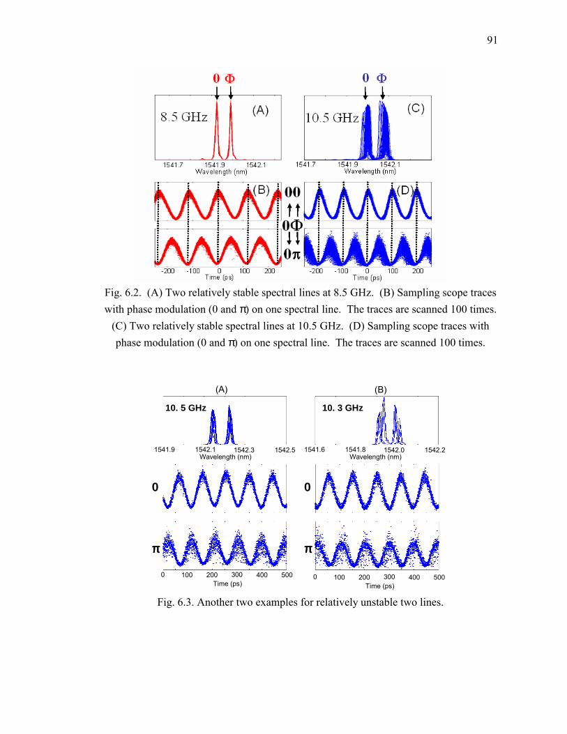
91
Fig. 6.2. (A) Two relatively stable spectral lines at 8.5 GHz. (B) Sampling scope traces with phase modulation (0 and π) on one spectral line. The traces are scanned 100 times.
(C) Two relatively stable spectral lines at 10.5 GHz. (D) Sampling scope traces with phase modulation (0 and π) on one spectral line. The traces are scanned 100 times.
1541.9 1542.1 1542.3Wavelength (nm)
10. 5 GHz
0
ππππ
0 100 200Time (ps)
300 400 500
1541.6 1541.8 1542.0Wavelength (nm)
1542.2
0 100 200Time (ps)
300 400 500
10. 3 GHz
0
ππππ
1542.5
(A) (B)
Fig. 6.3. Another two examples for relatively unstable two lines.

92
7. WIDTH AND WAVELENGTH TUNABLE OPTICAL RZ PULSE GENERATION AND RZ-TO-NRZ FORMAT
CONVERSION AT 10 GHZ USING SPECTRAL LINE-BY-LINE CONTROL
In this chapter, we will show the applications of line-by-line pulse shaping for RZ
(return-to-zero) pulse generation and RZ-to-NRZ (non-return-to-zero) format conversion [90].
7.1 Width and Wavelength Tunable Optical RZ Pulse Generation
Return-to-zero (RZ) pulses have been widely used in optical fiber communication systems and optical networks, including RZ format transmission, soliton systems, optical time-division-multiplexing, optical code-division-multiple-access, and optical packet generation. For example, RZ formats rather than non-return-to-zero (NRZ) formats have been applied in long-haul fiber transmission systems to extend transmission distance due to a possible higher tolerance to many fiber transmission impairments [91,92]. As a result, the characteristics of RZ pulses in such systems play a critical role in optimizing system performance. Therefore, tunable RZ pulse generation is highly desirable in system contexts. Tunable width RZ pulses have been demonstrated based on various techniques [92-95]. The techniques in reference [92,93] require electrical modulation which is difficult at high bit rates and/or shorter pulses. Optical tunable width RZ pulse generation has also been demonstrated [94,95], but relies on a relatively complicated nonlinear optical processing scheme with higher optical power requirement and lower efficiency, and/or limited width/wavelength tunable range. In this letter, we demonstrate for the first time to our knowledge a linear optical technique for tunable RZ pulse generation with large tunable wavelength range (1532~1562 nm) and pulse width range (~3-50 ps) at 10 GHz repetition rate based on spectral line-by-line pulse shaping of a mode-locked laser. All-optical RZ-to-NRZ format conversion is also demonstrated using this method, which is desirable in optical networks where spectral efficiency is more important than transmission distance since the NRZ format is more spectrally efficient.

93
In the frequency domain, mode-locked laser pulses are characterized by a series of discrete spectral lines (optical frequency comb) with the frequency interval equal to the longitudinal mode spacing of the laser, or equivalently to the pulse repetition rate. The pulse width is proportional to the inverse of the spectral bandwidth, or roughly speaking, the number of the spectral lines. From the pulse shaping perspective, essentially full pulse shape control can be achieved if it is possible to independently manipulate individual spectral lines. Specifically, the wavelength and width of the pulses can be tuned within the envelope of the input spectrum. Here we use this line-byline pulse shaper for tunable optical RZ pulse generation.
Note that our line-by-line pulse shaper is finely adjusted to achieve zero-dispersion, which is confirmed by negligible broadening for 400 fs pulses passing through the pulse shaper without spectral filtering. Therefore, the added chirp on the generated RZ pulses is negligible. On the other hand, chirped RZ (CRZ) pulses are also useful for fiber transmission experiments to optimize system performance [91]. The pulse shaper can also be designed to generate RZ pulses with tailored chirp.
Our experiments are performed using a home-built harmonically mode-locked fiber laser producing ~3 ps (FWHM) pulses at 10 GHz with center wavelength that can be tuned from 1532 nm to 1562 nm as input to the pulse shaper. Fig. 7.1 shows the shaped spectra and corresponding waveforms, where the laser center wavelength is tuned to 1542 nm. The number of spectral lines is controlled by the slit width in the line-by-line pulse shaper. The waveforms in Fig. 7.1(a)~(d) are detected by a 50 GHz photo-diode and sampling scope after an optical amplifier. Fig. 7.1(a) shows 2 spectral lines separated by the 10 GHz laser repetition rate. The optical linewidths are limited by the 0.01 nm resolution of the optical spectrum analyzer used for this measurement. Other spectral lines are well blocked due to the high resolution line-by-line shaper. Since there are only two spectral lines, ideally the waveform intensity profile in the time domain corresponds to a cosine function (with a DC offset). The waveform in Fig. 7.1(a) indeed shows a cosine function with 50 ps width (FWHM). Fig. 7.1(b)-(d) show 3, 4 and 5 spectral lines transmitted through the line-by-line pulse shaper. Accordingly, the generated RZ pulses exhibit 33 ps, 25 ps and 20 ps widths respectively which clearly illustrates that tunable width optical RZ pulses have been produced. Since the waveform measurement is limited by the 50 GHz bandwidth photo-diode and sampling scope, for generated pulses shorter than 20 ps, we measure them by standard short pulse intensity cross-correlation measurement, where the un-shaped 3 ps pulse is used as the reference. Fig. 7.1(e)~(h) show 6, 10, 16 and all spectral lines transmitted by the line-by-line pulse shaper,
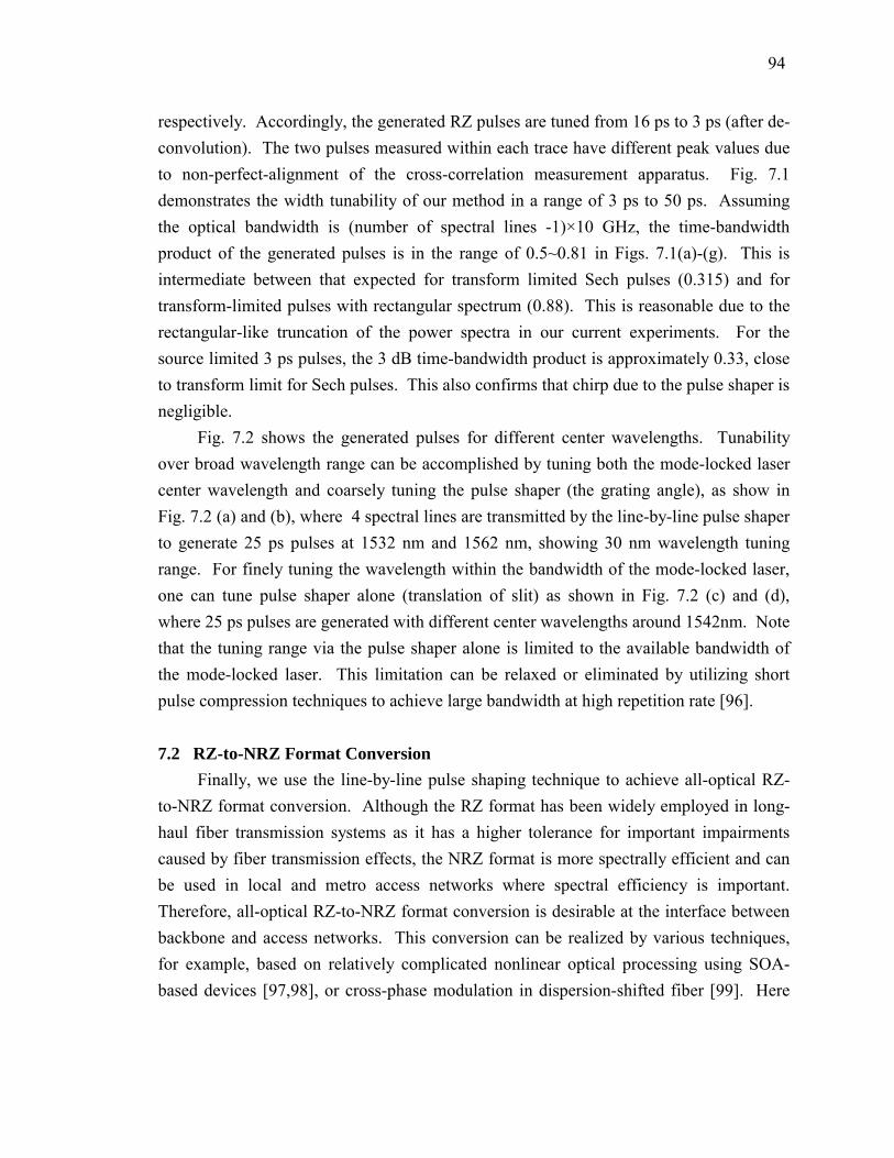
94
respectively. Accordingly, the generated RZ pulses are tuned from 16 ps to 3 ps (after de-convolution). The two pulses measured within each trace have different peak values due to non-perfect-alignment of the cross-correlation measurement apparatus. Fig. 7.1 demonstrates the width tunability of our method in a range of 3 ps to 50 ps. Assuming the optical bandwidth is (number of spectral lines -1)×10 GHz, the time-bandwidth product of the generated pulses is in the range of 0.5~0.81 in Figs. 7.1(a)-(g). This is intermediate between that expected for transform limited Sech pulses (0.315) and for transform-limited pulses with rectangular spectrum (0.88). This is reasonable due to the rectangular-like truncation of the power spectra in our current experiments. For the source limited 3 ps pulses, the 3 dB time-bandwidth product is approximately 0.33, close to transform limit for Sech pulses. This also confirms that chirp due to the pulse shaper is negligible.
Fig. 7.2 shows the generated pulses for different center wavelengths. Tunability over broad wavelength range can be accomplished by tuning both the mode-locked laser center wavelength and coarsely tuning the pulse shaper (the grating angle), as show in Fig. 7.2 (a) and (b), where 4 spectral lines are transmitted by the line-by-line pulse shaper to generate 25 ps pulses at 1532 nm and 1562 nm, showing 30 nm wavelength tuning range. For finely tuning the wavelength within the bandwidth of the mode-locked laser, one can tune pulse shaper alone (translation of slit) as shown in Fig. 7.2 (c) and (d), where 25 ps pulses are generated with different center wavelengths around 1542nm. Note that the tuning range via the pulse shaper alone is limited to the available bandwidth of the mode-locked laser. This limitation can be relaxed or eliminated by utilizing short pulse compression techniques to achieve large bandwidth at high repetition rate [96]. 7.2 RZ-to-NRZ Format Conversion
Finally, we use the line-by-line pulse shaping technique to achieve all-optical RZ-to-NRZ format conversion. Although the RZ format has been widely employed in long-haul fiber transmission systems as it has a higher tolerance for important impairments caused by fiber transmission effects, the NRZ format is more spectrally efficient and can be used in local and metro access networks where spectral efficiency is important. Therefore, all-optical RZ-to-NRZ format conversion is desirable at the interface between backbone and access networks. This conversion can be realized by various techniques, for example, based on relatively complicated nonlinear optical processing using SOA-based devices [97,98], or cross-phase modulation in dispersion-shifted fiber [99]. Here

95
we use line-by-line control, a linear technique, to achieve all-optical RZ-to-NRZ format conversion.
The generated RZ pulses are modulated and become an RZ format data stream. Fig. 7.3 (a) shows RZ format pulses modulated by a 10 Gb/s PRBS 223-1 data stream with 4 spectral lines (25 ps pulses) transmitted by the line-by-line pulse shaper. Compared with the un-modulated spectra shown in Fig. 7.1-2, each spectral line of the modulated spectra is broadened by the data modulation as shown in the figure. Here the line-by-line shaper is placed after the data modulator for experimental convenience. The modulated waveforms are detected by a 50 GHz photo-diode in which the RZ format is clear. In Fig. 7.3(b) only one spectral line is allowed to pass the line-by-line pulse shaper. As a result, the RZ format is converted to NRZ format, as shown by the eye-diagram also detected by the 50 GHz photo-diode. Higher spectral efficiency is clear for NRZ since it occupies less bandwidth with one spectral line rather than the bandwidth for RZ with multiple lines. The nonideal converted NRZ format (uneven �1� level) is caused by imprefect suppression of adjacent spectral lines (~20 dB suppression ratio) as shown by the log-scale optical power spectra in the figure insets. The �1� level can be made more flat by narrowing the pulse shaper filter bandwidth to suppress undesired lines more completely, but the eye-diagram becomes noisy and performance degrades. The increased noise is caused by optical frequency fluctuations in the mode-locked laser comb. Filtering to one single line (NRZ format) has the highest sensitivity to such fluctuation while filtering to produce multiple spectral lines (RZ format) has better tolerance, as evidenced by different noise levels in the eye-diagrams. The laser used in our system is relatively stable at 10 GHz mode-locking frequency (around 0.01 nm optical frequency fluctuations) making line-by-line pulse shaping and the current experiments possible in typical experimental environment conditions without additional control (for example, without temperature stabilization). The performance of the generated 25 ps RZ format and converted NRZ format are further confirmed by bit error rate measurement. Bit-error-rate (BER) measurements are shown in Fig. 7.3(c) for generated 25 ps RZ format (solid square) and converted NRZ format (solid circle) by line-by-line pulse shaping. There is about 4.2 dB power penalty at BER=10-9 for RZ-to-NRZ conversion mainly caused by the laser instability. To show the effectiveness of our approach, BER performances are also measured for RZ format (open square) and converted NRZ format (open circle) after 25 km single mode fiber transmission without dispersion compensation. The transmission power penalties (2.0 dB for RZ and 1.9 dB for NRZ) are mainly caused by fiber dispersion. The line-by-line pulse shaping performance is expected to be improved with
96
an optical-frequency-stabilized mode-locked laser. In our experiment only a single line-by-line pulse shaper is used to emulate the RZ-to-NRZ format conversion. In practice, one line-by-line pulse shaper can be used to generate the RZ format with desired wavelength and width while utilizing another line-by-line pulse shaper to implement RZ-to-NRZ format conversion.
In the current experiment the width of the RZ pulses is discretely tunable by simply changing the number of spectral lines. The pulse width can be continuously tuned by controlling not only the number of lines but also the relative amplitudes of the selected lines using a programmable amplitude line-by-line pulse shaper.
In conclusion, we have demonstrated for the first time to our knowledge tunable optical RZ pulse generation without additional chirp based on spectral line-by-line pulse shaping of a wavelength tunable mode-locked laser. Up to 30 nm wavelength tuning range (1532-1562 nm) and ~3-50ps pulse width range at 10 GHz repetition rate have been achieved. RZ-to-NRZ format conversion is also demonstrated using this technique without the need for any external pulse duplicator. This method can readily be applied to higher repetition rates for tunable RZ pulse generation and RZ-to-NRZ format conversion, for example, at 40 GHz.
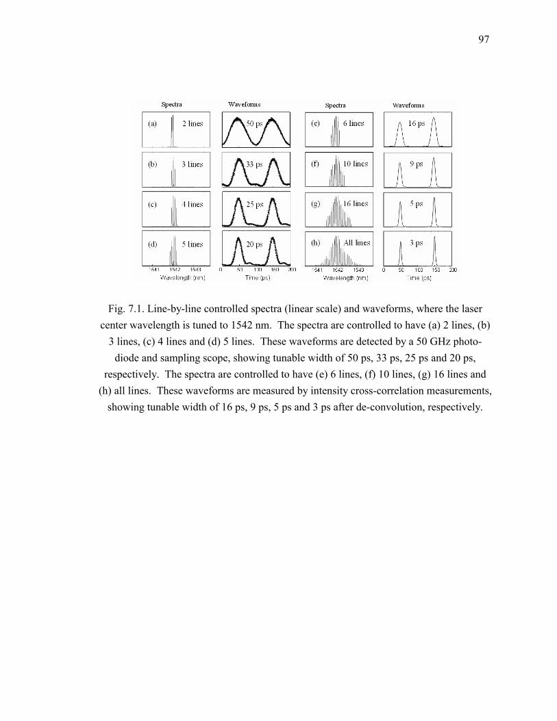
97
Fig. 7.1. Line-by-line controlled spectra (linear scale) and waveforms, where the laser center wavelength is tuned to 1542 nm. The spectra are controlled to have (a) 2 lines, (b)
3 lines, (c) 4 lines and (d) 5 lines. These waveforms are detected by a 50 GHz photo-diode and sampling scope, showing tunable width of 50 ps, 33 ps, 25 ps and 20 ps,
respectively. The spectra are controlled to have (e) 6 lines, (f) 10 lines, (g) 16 lines and (h) all lines. These waveforms are measured by intensity cross-correlation measurements,
showing tunable width of 16 ps, 9 ps, 5 ps and 3 ps after de-convolution, respectively.

98
Fig. 7.2. Line-by-line controlled spectra (linear scale) and waveforms, where 4 lines are transmitted through the line-by-line pulse shaper to generate 25 ps width pulses. Center
wavelength is tuned to (a) 1532 nm and (b) 1562 nm by tuning both the mode-locked laser center wavelength and coarsely tuning the pulse shaper (the grating angle). Center
wavelength is finely tuned around 1542 nm (c) and (d), by tuning pulse shaper alone (translation of slit).
Fig. 7.3. RZ-to-NRZ format conversion by line-by-line pulse shaping. Spectra and eye-
diagrams for (a) data modulated RZ format with 4 spectral lines, (b) converted NRZ format with only one spectral line. Inset figures show the spectra in log scale. (c) Bit-
error-rate measurements for generated RZ format (solid square) and converted NRZ format (solid circle) by line-by-line pulse shaping; RZ format (open square) and
converted NRZ format (open circle) after 25 km single mode fiber transmission without dispersion compensation.
99
8. LINE-BY-LINE PULSE SHAPING CONTROL FOR OPTICAL ARBITRARY WAVEFORM GENERATION
In this chapter, we will demonstrate Line-by-line pulse shaping control for optical
arbitrary waveform generation [100]. Fig. 8.1 shows line-by-line pulse shaper used in thie experiment, which has better
resolution than those used in chapter 6 and chapter 7. A fiber coupled Fourier-Transform pulse shaper is constructed in a reflective geometry. A fiber-pigtailed collimator and subsequent telescope take the light out of fiber and magnify the beam size to ~18 mm diameter on the 1200 grooves/mm grating in order to enhance the pulse shaper resolution. Discrete spectral lines making up the input short pulse are diffracted by the grating and focused by the lens with 1000 mm focal length. A fiberized polarization controller (PC) is used to adjust for horizontal polarization on the grating. A 2×128 pixel liquid crystal modulator (LCM) array with a calcite polarizer (> 100,000:1 extinction ratio) on the input face is placed just before the lens focal plane to independently control both amplitude and phase of individual spectral lines. The LCM (Cambridge Research & Instrumentation, Inc.) in our experiment is fully integrated with control electronics and software. The update speed of LCM is on the order of tens of ms to ~100 ms, limited by the liquid crystal relaxation time. The individual pixels of the LCM, arranged on 100 µm centers, can be electronically controlled independently to give amplitude and phase control with 12-bit resolution. A retro-reflecting mirror leads to a double-pass geometry, with all the spectral lines recombined into a single fiber and separated from the input via an optical circulator. The fiber-to-fiber insertion loss is 11.6 dB (including circulator loss), which includes all optical component losses as well as loss incurred in focusing back into the 9 µm fiber mode after the pulse shaper. The passband width, measured by scanning a tunable, narrow-linewidth, continuous-wave laser with the LCM replaced by a narrow slit, is 2.6 GHz at the 3 dB points, as shown in the inset. To the best of our knowledge, this is the highest resolution ever reported for a grating-based pulse shaper. The unprecedented high resolution makes accurate and independent control of individual

100
spectral lines possible and enables true line-by-line pulse shaping control, potentially over a broad optical band.
We note that in addition to LCMs, other spatial light modulators are also well known in pulse shaping [47]. Line-by-line pulse shaping experiments analogous to what is reported here should also be possible using other spatial light modulator technologies, provided that the key requirement of very high spectral resolution for clear separation of adjacent spectral lines is met.
Our experiments are performed using a home-built harmonically mode-locked fiber laser producing 3 ps (full width at half maximum) pulses at 10 GHz repetition rate with center wavelength of 1542.5 nm. The repetition rate, selected to ensure that the spectral line spacing exceeds the pulse shaper resolution, is especially appropriate for eventual applications in optical communications. Each spectral line is spaced by 200 µm, corresponding to 2 LCM pixels. The frequency offset of the mode-locked comb is not actively stabilized; instead we exploit the passive frequency stability of the mode-locked comb, ~1 GHz over the time scale of our experiments (ten times below the comb spacing). This suffices for these first proof-of-concept experiments on line-by-line pulse shaping control for O-AWG under typical laboratory environmental conditions without additional controls (e.g., temperature stabilization). To achieve a larger number of spectral lines, the 3 ps pulses are compressed to 400 fs by a dispersion-decreasing fiber soliton compressor. Either 3 ps or 400 fs pulses at 10 GHz repetition rate are used as input to the pulse shaper according to the required bandwidth for the specific demonstration. Fig. 8.2 shows power spectra (log plots) and resultant time-domain intensity waveforms when the pulse shaper is used to select just two spectral lines out of the mode-locked frequency comb. Data are shown for spectral line separations of 10, 20, and 100 GHz (Figs. 8.2(A-C), 3 ps input pulses) and 400 and 500 GHz (Figs. 8.2(E-F), 400 fs input pulses). The measured optical linewidths are limited by the 0.01 nm resolution of the optical spectrum analyzer. The power spectra in Figs. 8.2(A-C) are also plotted on a linear scale (insets) in order to clearly show the ability to control the relative amplitudes of the two selected lines (in general they don�t have equal amplitudes before pulse shaping) and very strongly suppress deselected spectral lines (deselected lines are not visible in the linear plots). The log plots reveal that deselected spectral lines are suppressed by greater than 31.5 dB for 10 GHz, 29 dB for 20 and 100 GHz, 28 dB for 400 GHz, and 26 dB for 500 GHz.
The intensity waveform resulting from selection of two spectral lines is ideally a cosine function with DC offset. Data shown in the figure reveal cosines with periods of
101
100, 50, 10, 2.5, and 2 ps, respectively, as expected. These data were measured after an optical amplifier, using either a 50 GHz bandwidth photodiode and sampling oscilloscope (10 and 20 GHz) or standard short optical pulse intensity cross-correlation techniques (100-500 GHz). The pulse shaper itself is able to afford much higher frequency cosine waveforms, but here is limited by the available optical bandwidth from the laser and by the measurement process (shorter reference pulses are required to measure higher frequency cosine waveforms with shorter period). This limitation can be relaxed or eliminated by utilizing short pulse compression techniques to achieve large bandwidth at high repetition rate. The increased fluctuations and distortions in the cosine waveforms at higher frequencies (especially 400 and 500 GHz) arise due to decreased optical power as the selected lines approach the edge of the input spectrum (10 µW optical power for the two lines with 500 GHz separation), which increases susceptibility to imperfect suppression of deselected lines and optical amplifier noise. Nevertheless, these data clearly demonstrate the potential to synthesize modulations over a very broad frequency range.
It is essential to note that strong suppression of deselected spectral lines is critical for accurate waveform generation. To validate this point, simulations are performed in which suppression is degraded for the nearest neighbors to the selected spectral lines. Fig. 8.2(D) shows the case of a spectral line pair separated by 100 GHz, with suppression of adjacent lines limited to 18 dB (consistent with the nearest neighbor suppression ratio for our previous, lower resolution pulse shaper in chapter 6). Even at 18 dB suppression, coherent crosstalk from the weak undesired lines leads to huge intensity variation in the time-domain waveform (the ratio between distorted cosine waveform envelope peak to valley is ~2.8)! Furthermore, in experiments one might expect even worse waveform degradation for the same limited suppression ratio, since not only imperfectly suppressed adjacent lines, but also undesired nonadjacent lines, are likely to play a role. The dramatic effect in the time domain caused by small unsuppressed lines can be understood in the following way. Considering the example in which suppression is degraded for the nearest neighbors to the selected spectral lines as in Fig. 8.2(D), if the four equal nearest neighbors have normalized intensity of a , then the field amplitude is a . The waveform envelope peak intensity is reached when all the four neighbors are in phase with the two selected lines, which gives a relative intensity of 2)42( a+ . Similarly, the waveform
intensity envelope valley is reached when all the four neighbors are out of phase with the two selected lines, which yields a relative intensity of 2)42( a− . Using a suppression
102
value of 18 dB, the calculated ratio between peak and valley is ~2.8, which is consistent with the simulation in Fig. 8.2(D). In our experiments, the adjacent lines have unequal powers and nonadjacent lines also show up. But if we assume only one adjacent line is dominant (which is likely in the experiments), a similar simple calculation applies. In such case, the intensity envelope peak is 2)2( a+ and the valley is 2)2( a− .
Considering the experimental example of Fig. 8.2(C) with 29 dB suppression, the calculated ratio between peak and valley using this model is ~1.074, which agrees well with the calculated value based on the experimental data (~1.069). It is clear that the high pulse shaper resolution in our current experiments, allowing much stronger suppression of deselected spectral lines, is key for high quality line-by-line pulse shaping control for O-AWG. Besides the pulse shaper resolution, the suppression ratio of deselected spectral lines is also affected by the amplitude control capability of the LCM.
In principle, any periodic waveform can be constructed from a complete set of harmonic (cosine and sine) waveforms. Fig. 8.3 shows an example of line-by-line pulse shaping control for such O-AWG by manipulating multiple spectral lines over a broad optical band. Two pairs of spectral lines are simultaneously selected and controlled, with 10 GHz frequency separation within each pair and 410 GHz center-to-center frequency separation between pairs (Fig. 8.3(A)). There is a clear relationship between the spectral lines in the frequency domain and the waveform generated in the time domain: the 100 ps macro period of the waveform envelope is determined by the 10 GHz spacing between lines within a single pair, while the ~2.44 ps micro period of waveform oscillation is determined by the average 410 GHz spacing between pairs (Fig. 8.3(B)). To demonstrate fine scale waveform control, a π phase shift is applied to one pair of spectral lines while keeping the spectral amplitude essentially unchanged. The resulting time domain waveform should be out of phase compared with the waveform without the phase shift, exactly as seen in the zoomed figures. The finite contrast of the waveform oscillation minimum points, which should go to zero theoretically, is explained by the finite duration of the 400 fs reference pulses used for the measurement. These examples demonstrate an unprecedented capability for true line-by-line pulse shaping control, with waveform manipulation at both macro and micro scale simultaneously. It should also be noted that the pulse shaping technique affords control over both temporal intensity and phase, as is now well known [47], although our measurements here are sensitive only to intensity.
Fig. 8.4 shows another example of line-by-line pulse shaping control for O-AWG that highlights the fidelity of our method. Four spectral lines (five consecutive lines with

103
the center line blocked, Fig. 8.4(A)) are selected within a relatively narrow bandwidth to ease comparison with a theoretical calculation. By applying the same amplitude modulation ([1 1 0 1 1]) but different phase modulation ([π 0 − 0 π] or [0 π − 0 π]), two distinct waveforms are generated. The intensity cross-correlation measurements are in almost perfect agreement with and are essentially indistinguishable from the calculations (black circles) based on the Fourier transform of the nominal amplitude and phase patterns imparted onto the spectral lines (Fig. 8.4(B-C)). The key point is that one can now synthesize optical waveforms with desired amplitude and phase, high fidelity, and 100% duty factor, by manipulating the individual spectral lines from a mode-locked frequency comb. It should also be noted that to clearly illustrate the relationship between the time and frequency domains, intensity and phase control are demonstrated in a binary fashion. As is well known, both intensity and phase gray level control can be readily achieved [47] using an LCM. Actually, the power spectra shown Figs. 8.2(A-C), visible on a linear scale in the insets, have been power equalized with the LCM, which is already an example of gray level intensity manipulation.
One immediate application of line-by-line pulse shaping control for O-AWG is for generation of arbitrary radio-frequency electrical waveforms (RF-AWG). Fig. 8.4(D-E) show sampling oscilloscope measurements of the electrical output generated when the optical waveforms of Figs. 8.4(B-C) drive a 50 GHz photo-diode. Such highly structured, high frequency, and broadband radio-frequency waveforms are impossible to implement using current electrical AWG technology which is typically limited to ~1 GHz [101]; however, the same waveforms are narrow-band from the optics point of view and can be implemented easily as shown here. The slight distortions of the RF waveforms compared with the driving optical signals are caused by the limited bandwidth of the photodiode and sampling scope, which could be precompensated (for example, to achieve two equal main peaks in Fig. 8.4(E)) by appropriately modifying the control signals to the optical driving waveforms. RF-AWG has the potential to impact fields such as ultrawideband (UWB) wireless [102], which uses subnanosecond electrical bursts for communications and sensing, and impulse radar, where the use of highly structured transmit waveforms designed to optimize discrimination between different scattering targets has been proposed [103].

104
MirrorGrating
LCM
Lens
PC Input pulse from mode-locked
laser at 10 GHz
Collimator
Output shaped pulse
f f
Telescope
Free spaceFiber
2 1
3
Circulator
Spectral Lines
1542.65 1542.7 1542.75Wavelength (nm)
2.6 GHz
MirrorGrating
LCM
Lens
PC Input pulse from mode-locked
laser at 10 GHz
Collimator
Output shaped pulse
f f
Telescope
Free spaceFiberFree spaceFiber
2 1
3
Circulator
Spectral Lines
1542.65 1542.7 1542.75Wavelength (nm)
2.6 GHz
1542.65 1542.7 1542.75Wavelength (nm)
2.6 GHz
1542.65 1542.7 1542.75Wavelength (nm)
2.6 GHz
Fig. 8.1. Experimental apparatus for arbitrary waveform generation using line-by-line pulse shaper. The inset figure shows a measured 3 dB passband of 2.6 GHz. LCM:
liquid crystal modulator. PC: polarization controller.
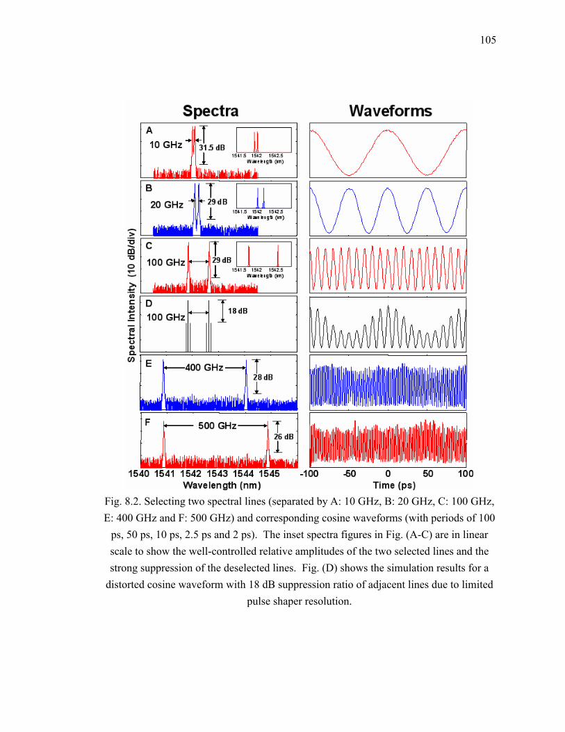
105
Fig. 8.2. Selecting two spectral lines (separated by A: 10 GHz, B: 20 GHz, C: 100 GHz, E: 400 GHz and F: 500 GHz) and corresponding cosine waveforms (with periods of 100
ps, 50 ps, 10 ps, 2.5 ps and 2 ps). The inset spectra figures in Fig. (A-C) are in linear scale to show the well-controlled relative amplitudes of the two selected lines and the strong suppression of the deselected lines. Fig. (D) shows the simulation results for a
distorted cosine waveform with 18 dB suppression ratio of adjacent lines due to limited pulse shaper resolution.

106
Fig. 8.3. Selecting four spectral lines, in which two lines in each pair are separated by 10 GHz and the two inner lines between the two pairs are separated by 400 GHz. The center to center separation of the line pairs is 410 GHz. The resulting waveforms have 100 ps
macro period (corresponding to 10 GHz) and 2.44 ps micro period (corresponding to 410 GHz). The red and blue waveforms are controlled to be out of phase by applying π phase
shift on one pair of spectral lines, as shown in the zoomed figures.

107
Fig. 8.4. Selecting four spectral lines (five consecutive lines with center line blocked).
(B,C) Waveforms measured by intensity cross-correlation with different applied spectral phases (red and blue curves). Calculations (black circles) are essentially indistinguishable from the data, showing the high fidelity of the generated waveforms. (D,E) Waveforms
are detected by a 50 GHz photo-diode and measured by sampling scope in persistent mode to demonstrate radio frequency arbitrary waveform generation (RF-AWG).

108
9. OPTICAL ARBITRARY WAVEFORM GENERATION AND CHARACTERIZATION USING SPECTRAL LINE-BY-LINE
CONTROL
In chapter 8 we discussed line-by-line pulse shaping for optical arbitrary
waveform generation (O-AWG). One immediate issue related to O-AWG is characterization to ensure that the desired waveform has been generated correctly. Commercial high speed photo-diodes have bandwidths limited to ~60 GHz, which is insufficient for most O-AWG measurement. Furthermore, the temporal phase information is lost since the photo-diode is a square-law device. Various optical techniques have been developed to completely characterize the intensity and phase of optical pulses, based on the concept of spectrography (e.g, FROG) [104], interferometry (e.g, SPIDER) [105] and tomography [106]. Among the available possibilities, an interferometry-based method [107-109] is particularly appealing for the characterization of O-AWG generated waveforms by spectral line-by-line pulse shaping since this method also relies on spectral line-by-line control. In this chapter, we integrate both the functionalities of O-AWG and its characterization based on spectral line-by-line control as an enabling technology for high fidelity O-AWG [110]. 9.1 Experimental Setup
Fig. 9.1 shows our experimental setup, which includes the O-AWG section and the characterization section. In the O-AWG section, a home-built harmonically mode-locked fiber laser is used to produce near transform-limited 3 ps (full width at half maximum) pulses at 1542.5 nm center wavelength with a repetition rate of 10.0 GHz. The frequency offset of the mode-locked comb is not actively stabilized; instead we exploit the passive frequency stability of the mode-locked comb, ~1 GHz over the time scale of our experiments (ten times below the comb spacing). This suffices for our experiments under typical laboratory environmental conditions without additional controls (e.g., temperature stabilization). The mode-locked laser is followed by a programmable pulse shaper for O-AWG using spectral line-by-line pulse shaping.
109
Erbium doped fiber amplifiers (EDFA) are used for loss compensation. In the characterization section, a second pulse shaper is used to filter only two spectral lines (this is monitored by an optical spectrum analyzer). The resulting cosine waveform (with a DC offset) from the beat of these two spectral lines is detected by a 50 GHz photo-diode and measured by a sampling oscilloscope. The details of this measurement method can be found in [107], and will be briefly described later.
Spectral line-by-line control for O-AWG and its characterization are accomplished by high resolution fiber coupled Fourier-Transform pulse shapers in a reflective geometry. In order to achieve line-by-line pulse shaping, great care is taken in the pulse shaper design to improve resolution. For each pulse shaper, a fiber-pigtailed collimator and subsequent telescope take the light out of fiber and magnify the beam size on the diffraction grating. Discrete spectral lines making up the input short pulse are diffracted by the grating and focused by a lens. A fiberized polarization controller (PC) is used to adjust for horizontal polarization on the grating for high diffraction efficiency. A 2×128 pixel liquid crystal modulator (LCM) array with a polarizer on the input face is placed just before the lens focal plane to independently control both the amplitude and phase of individual spectral lines. A retro-reflecting mirror at the lens focal plane leads to a double-pass geometry, with all the spectral lines recombined into a single fiber and separated from the input via an optical circulator. For the characterization pulse shaper, a slit can be used to replace the LCM since only two lines need to be selected. Actually, in our experiments, in addition to a LCM, a slit is used to assist in blocking unwanted lines when the contrast ratio of intensity modulation applied by the LCM is not sufficient. The parameters of both pulse shapers are listed in table 9.1. Using a narrow slit, the measured passband of the line-by-line pulse shapers have a minimum 3 dB passband width of 5.0 GHz, and 2.6 GHz for the first (generation) and second (measurement) pulse shapers respectively. Both pulse shapers have high resolution to afford line-by-line control at the ~10 GHz laser repetition rate, which is appropriate for applications in optical communications. For accurate line-by-line control, the spectral line spacing of the mode-locked laser (the repetition rate) has to match the spatial spacing of the pixels (or integer multiple of the pixel spacing). This can be implemented by tuning the grating diffraction angle and/or tuning the repetition rate of the actively mode-locked fiber laser. Note that our line-by-line pulse shaper is finely adjusted to achieve zero-dispersion, which is confirmed by negligible broadening for 3 ps pulses passing through the pulse shaper without spectral filtering. This is important for both pulse shapers. For the shaper in the O-AWG section, zero-dispersion is important for accurate and known phase control
110
(since, without filtering, input transform-limited pulses will remain transform-limited after the shaper). For the second pulse shaper (in the characterization section), zero-dispersion ensures accurate phase characterization since no extra dispersion is inferred onto the waveforms to be measured.
The loss of the line-by-line pulse shapers in our current setup is higher than the loss of the relatively low resolution, fiber coupled pulse shapers we demonstrated before (4.0 dB). This mainly arises from the large size collimated beam after the telescope. The laser beam size makes it more difficult to focus the beam back into the 9 µm fiber mode after the pulse shaper, most likely due to lens aberrations (in the pulse shaper and in the telescope).
Note that the update speed of LCM is on the order of tens of ms to ~100 ms, limited by the liquid crystal relaxation time. Therefore, pulse shaping experiments to date, including those reported here, are generally constrained to generate waveforms periodic at the repetition rate of the mode-locked laser source. To generate waveforms with different period, the repetition rate of the laser should be changed. Accordingly, the pulse shaper design has to be modified to match the spectral line separation (the repetition rate of the laser). Alternatively, if a fast spatial light modulator technology capable of update at the laser repetition rate were to become available, then aperiodic waveforms or waveforms with periodicities different than that of the input laser could be generated via appropriate reprogramming of the spatial light modulator on a pulse by pulse basis.
9.2 Results and Discussions
First, the principle of pulse measurement is briefly sketched; further detail can be found in [107]. Considering any two spectral lines selected by the pulse shaper at the characterization section, the field in the frequency domain can be expressed as
)exp()()()( θδβδ jffffM −⋅∆−⋅+= (9.1)
where δ(⋅) represents the impulse function, β and θ represent the relative intensity and phase between the two spectral lines, and ∆f is the frequency spacing between two lines. ∆f usually equals the mode-locked laser repetition rate frep if an adjacent two lines are selected from the mode-locked laser. But if there are lines missing between them, ∆f would be an integer multiple of frep. In the time domain, the intensity profile can be obtained by Fourier Transform as
[ ])(2cos21
)2cos(21)( 2
τπββ
θπββ
−∆⋅++=
−∆⋅++=
tf
fttm (9.2)
111
where πτθ 20
⋅=T
, T0=1/∆f is the cosine waveform period, and τ is the cosine waveform
temporal delay. Clearly, the spectral phase difference θ between the two spectral lines is directly related to the temporal phase of the cosine waveform, which in turn is directly related to the measurable quantity of the cosine waveform temporal delay τ. After all the spectral phase differences have been measured by filtering adjacent pairs of spectral lines consecutively, the whole set of spectral phases can be obtained by simply cascading all the phase differences. The spectral intensity can be measured separately using an optical spectrum analyzer. With the measured spectral intensity and phase, the temporal waveform can be calculated by a Fourier transform. This measurement method can be considered as a line-by-line version of those demonstrated in [111, 112].
To show both the accuracy of the phase profile applied by the pulse shaper and the accuracy of the measurement method, first we use just the second (characterization) pulse shaper. The second pulse shaper simultaneously selects two lines and applies a phase shift on one of the lines. We then measure the temporal delay. Fig. 9.2(a) shows the spectrum with two lines selected in both linear scale and log scale (inset), and the laser running at 10.0 GHz repetition rate. The two lines are equalized to have the same height, which is made possible by the accurate intensity control afforded by the pulse shaper. Compared with previous pulse measurements using this method [107], one important improvement is that the undesired lines are almost completely suppressed (higher than 35 dB suppression ratio in this example - undesired lines are buried in the noise background). This is a direct consequence of the high resolution of our pulse shaper. Such high suppression ratio is critically important to avoid distortion of the cosine waveform and thus accurate determination of temporal delay [107]. Fig. 9.2(b) shows the intensity profiles of waveforms in the time domain by applying different phase shifts on one of the lines � detected by a 50 GHz photodiode and measured by a sampling oscilloscope (averaged 20 times). All four waveforms indeed show a cosine function with a temporal delay determined by the applied phase shift according to eq.(9.2). With respect to the cosine waveform without phase shift (0 ps delay), the ideal relative delays should be 25 ps, 50 ps, 75 ps corresponding to π/2, π and 3π/2 relative phase shifts (considering the 100 ps period). The measured values are 26 ps, 50 ps, 75 ps respectively, almost perfectly agreeing with the ideal values. The measurement accuracy is limited by the sampling scope, which has a timing step size of 1 ps in our system. From these experiments, we show that both the phase shift applied by the LCM and the phase measurement using line-by-line control are highly accurate.

112
In previous work (chapter 8) and in Fig. 9.2, we have already demonstrated that O-AWG can be achieved with high fidelity after taking great care (including careful intensity/phase calibration of the LCM, improved pulse shaper resolution to reduce crosstalk between spectral lines, and matching the spectral line spacing to the pixel spacing). However, spectral phase errors may still occur in practical applications. In such cases, the waveform characterization capability will be critical and should be integrated to the O-AWG functionality for high fidelity waveform generation. This is similar to the fact that advances in the frontier of short pulse generation benefit significantly from progress in ultrashort pulse measurement techniques. Since the spectral intensity can be monitored by an optical spectrum analyzer, such feedback information would be sufficient to achieve accurate line-by-line intensity control. The difficult part is possible uncertainties in the spectral phases applied to the individual lines, which would significantly affect the temporal waveforms [104]. Therefore, both optical arbitrary waveform generation and characterization functionalities will be critical to achieve user-specified waveforms with high fidelity. It is clear that the setup in Fig. 9.1 meets both the requirement for O-AWG and for its characterization. Both functions are implemented through spectral line-by-line control, which is especially promising for practical applications.
We now return to experiments using both pulse shapers, one for generation and the other for measurement. Here, we intentionally introduce errors into the generation section in order to emphasize the importance of the characterization section. For this purpose, we simply mismatch the spectral line spacing and the LCM pixel spacing in the first pulse shaper. In particular, we set the grating incident angle to give 8.5 GHz optical frequency spacing per LCM pixel while the repetition rate of the laser is set at 10.0 GHz. Such mismatch introduces phase and intensity errors due to the finite beam size of individual spectral lines (some spectral lines will overlap more than one pixel). Note that any other kind of phase error can be monitored exactly in the same way regardless of origin.
In the first example, we generate a waveform corresponding to five spectral lines with one line missing as shown in Fig. 9.3(a). In addition to the spectral intensity manipulation, the nominal phase profile applied by the first pulse shaper to the selected spectral lines is [0.30π, 0, -, 1.00π, 0.40π]. The - symbol is used here to indicate that the spectral line at that position is not present as discussed. The phase errors caused by the mismatch mentioned above are verified by the measurement as shown in Fig. 9.4. Every pair of two spectral lines is selected by the characterization pulse shaper and the delay of
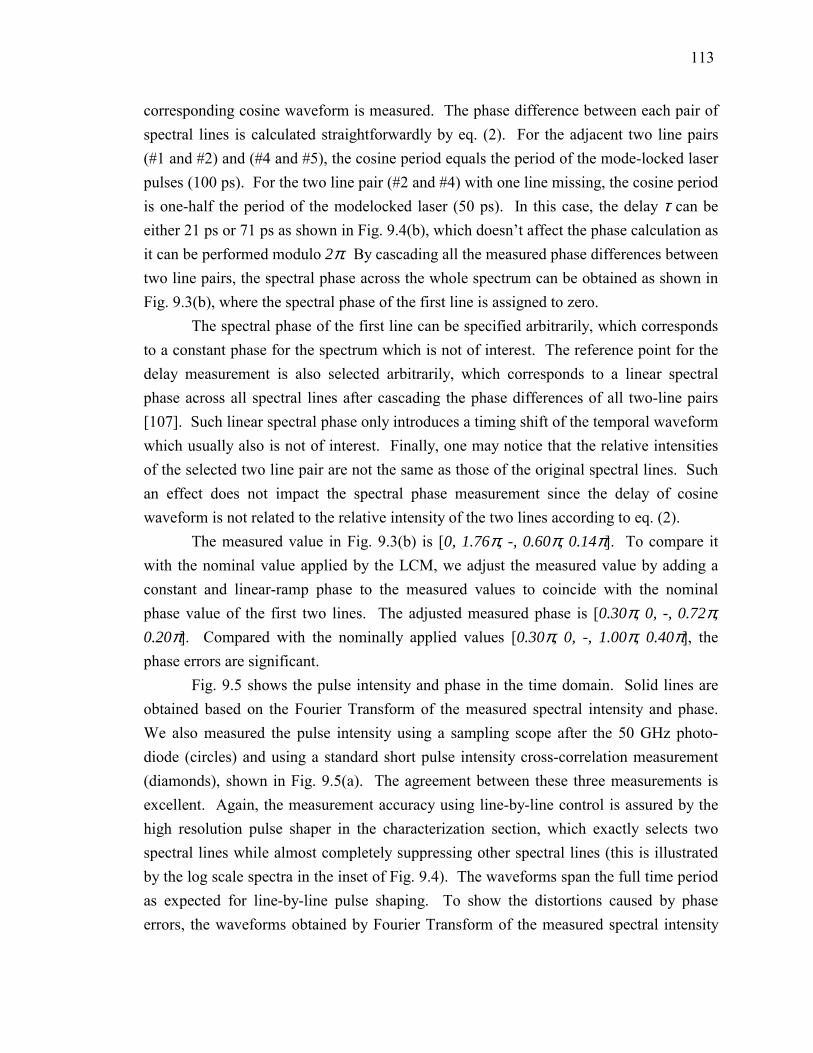
113
corresponding cosine waveform is measured. The phase difference between each pair of spectral lines is calculated straightforwardly by eq. (2). For the adjacent two line pairs (#1 and #2) and (#4 and #5), the cosine period equals the period of the mode-locked laser pulses (100 ps). For the two line pair (#2 and #4) with one line missing, the cosine period is one-half the period of the modelocked laser (50 ps). In this case, the delay τ can be either 21 ps or 71 ps as shown in Fig. 9.4(b), which doesn�t affect the phase calculation as it can be performed modulo 2π. By cascading all the measured phase differences between two line pairs, the spectral phase across the whole spectrum can be obtained as shown in Fig. 9.3(b), where the spectral phase of the first line is assigned to zero.
The spectral phase of the first line can be specified arbitrarily, which corresponds to a constant phase for the spectrum which is not of interest. The reference point for the delay measurement is also selected arbitrarily, which corresponds to a linear spectral phase across all spectral lines after cascading the phase differences of all two-line pairs [107]. Such linear spectral phase only introduces a timing shift of the temporal waveform which usually also is not of interest. Finally, one may notice that the relative intensities of the selected two line pair are not the same as those of the original spectral lines. Such an effect does not impact the spectral phase measurement since the delay of cosine waveform is not related to the relative intensity of the two lines according to eq. (2).
The measured value in Fig. 9.3(b) is [0, 1.76π, -, 0.60π, 0.14π]. To compare it with the nominal value applied by the LCM, we adjust the measured value by adding a constant and linear-ramp phase to the measured values to coincide with the nominal phase value of the first two lines. The adjusted measured phase is [0.30π, 0, -, 0.72π, 0.20π]. Compared with the nominally applied values [0.30π, 0, -, 1.00π, 0.40π], the phase errors are significant.
Fig. 9.5 shows the pulse intensity and phase in the time domain. Solid lines are obtained based on the Fourier Transform of the measured spectral intensity and phase. We also measured the pulse intensity using a sampling scope after the 50 GHz photo-diode (circles) and using a standard short pulse intensity cross-correlation measurement (diamonds), shown in Fig. 9.5(a). The agreement between these three measurements is excellent. Again, the measurement accuracy using line-by-line control is assured by the high resolution pulse shaper in the characterization section, which exactly selects two spectral lines while almost completely suppressing other spectral lines (this is illustrated by the log scale spectra in the inset of Fig. 9.4). The waveforms span the full time period as expected for line-by-line pulse shaping. To show the distortions caused by phase errors, the waveforms obtained by Fourier Transform of the measured spectral intensity
114
but using the nominal spectral phase applied by the LCM is also plotted (dashed lines). Compared with the other traces, this calculation of the temporal intensity deviates significantly. In this particular case, the difference between the calculated temporal phases is small; nevertheless, this simple example shows that waveform monitoring can play an important role to achieve desired results in O-AWG.
Fig. 9.6 shows an example with thirteen spectral lines for which the effect of phase errors may be even more prominent. The thirteen spectral lines cover around 15 pixels of the generation pulse shaper. Since the mismatch is larger than 1 pixel, it is impossible to assign the nominal spectral phase applied by the LCM to individual spectral lines. A pure cubic spectral phase in pixel number is applied to the spectral lines by the first pulse shaper, with 0 phase shift approximately at the center. But the actual phase profile as a function of individual spectral line is unknown due to the mismatch. The mismatch can also be noticed from the measured spectral intensity in Fig. 9.6(a) where some of the spectral lines are attenuated more if they are located between two pixels. This phenomenon results from diffraction effects experienced by the frequency components falling at phase transition regions of the LCM in the pulse shaper.
The measured phase profile using line-by-line control in the characterization shaper is plotted in Fig. 9.6(b). If the phase is unwrapped as shown in the inset, the cubic characteristic is clear. In order to compare it with the nominal phases applied by the LCM, the measured spectral phases of the 13 lines are adjusted by adding a constant and linear-ramp phase, shown in Fig. 9.7 along with the nominal phases corresponding to the 15 pixels of the LCM. For the nominal phases, the pixel positions are mapped onto wavelength using the known spatial dispersion (8.5 GHz/pixel). The center line (line #7) is assumed to be aligned with the center pixel (pixel #8). The adjusted value of constant and linear phase is chosen such that the center line (line #7) has the same phase shift (zero) as the center pixel (pixel #8) and the leftmost line (line #1) has the same phase shift as pixel #1. As expected, they are similar but with noticeable differences: (1) The largest discrepancies appear at the right edge. If we adjust phases such that the rightmost line (line #13) has the same phase shift as pixel #15, discrepancies appear at the left edge; (2) The measurement errors using line-by-line control becomes larger at the edges since the selected two lines at the edges have relatively small optical power and thus lower signal to noise ratio for the delay measurement; (3) The center line (line #7) is assumed to be aligned with the center pixel (pixel #8). However, the details of possible slight (less than one pixel) frequency offset are unknown.

115
Fig. 9.8 shows the pulse intensity and phase in the time domain. Solid lines are obtained based on the Fourier Transform of the measured spectral intensity and phase, which agree well with the intensity cross-correlation (diamonds) in Fig. 9.8(a). The temporal intensity shows an oscillatory tail � a property of cubic spectral phase. Again, the waveforms span the full time period as expected. From the point view of O-AWG, not only is the desired temporal intensity important, but the temporal phase may also need to be tailored in a specified way. In such cases, temporal phase monitoring would be as important as temporal intensity monitoring for O-AWG applications. The temporal phase profile shown in Fig. 9.8(b) illustrates that such functionality has been automatically included in the current setup.
Accurately determined phases for individual spectral lines could be very valuable feedback information for the first pulse shaper to generate targeted O-AWG signals if any phase errors occur. Usually, the phase errors are small, and the error correction could be simply implemented using measure-and-correct procedure with a small number of iterations, even without knowledge of the origin of the phase errors.
In summary, we have demonstrated for the first time to our knowledge simultaneous optical arbitrary waveform generation and characterization using spectral line-by-line control. User specified optical waveform is related to the intensity and phase of the spectral lines by a Fourier Transform. Complete characterization of O-AWG is important to monitor and thus to improve its performance. With these integrated functionalities, phase errors can be monitored. With appropriate correction procedures, it will be possible to achieve O-AWG with high fidelity even if such errors occur.

116
10GHz mode-locked laser
pulse shaperEDFA
Spectra
Pulses
pulse shaper EDFA
CharacterizationO-AWG
Sampling Scope
Photo-diode
OSA
EDFA: Erbium doped fiber amplifier. OSA: Optical spectrum analyzer. : Coupler
#1 #2
t
λλλλ
t t
λλλλλλλλ
10GHz mode-locked laser
pulse shaperEDFA
Spectra
Pulses
pulse shaper EDFA
CharacterizationO-AWG
Sampling Scope
Photo-diode
OSA
EDFA: Erbium doped fiber amplifier. OSA: Optical spectrum analyzer. : Coupler
#1 #2
t
λλλλ
t t
λλλλλλλλ
Fig. 9.1. Experimental setup for O-AWG and its characterization using spectral line-by-
line control.
Table 9.1. Line-by-line pulse shaper parameters
Collimated beam diameter before grating (mm) *
Grating lines (/mm)
Grating diffraction angle (degree)
Lens focal length (mm)
Shaper #1 18 1100 57 750 Shaper #2 18 1200 65 1000
Spectral coding Range at the LCM ∆λ (nm)
Minimum 3 dB bandwidth (GHz)
Resolution ** (µm)
Loss (dB) (including circulator)
Shaper #1 8.5 5.0 75 10.0 Shaper #2 4.5 2.6 80 10.0
*: Beam diameter is defined as intensity decreases to 1/e2 of peak value **: Resolution is defined as beam diameter at LCM layer. This value is calculated. The real beam diameter at LCM layer is likely larger than the calculated value due to lens aberrations.

117
(a)1541.8 1542 1542.2 1542.4 1542.6
Wavelength (nm)
1541.8 1542 1542.2Wavelength (nm)
10 d
B/d
iv0 Φ
0 ps
Time (ps)-100 -50 0 50 100
75 ps
50 ps
26 ps
(b)
0
π/2
π
3π/2
(a)1541.8 1542 1542.2 1542.4 1542.6
Wavelength (nm)
1541.8 1542 1542.2Wavelength (nm)
10 d
B/d
iv
1541.8 1542 1542.2Wavelength (nm)
10 d
B/d
iv0 Φ
0 ps
Time (ps)-100 -50 0 50 100
75 ps
50 ps
26 ps
(b)
0
π/2
π
3π/2
Fig. 9.2. (a) Two spectral lines selected. (b) Sampling scope traces with phase
modulation (0, π/2, π and 3π/2) on one spectral line. The traces are the average of 20 measurements.

118
#1
#2
1541.8 1542 1542.2Wavelength (nm)
10 d
B/d
iv#4
#5#3
1541.8 1542 1542.2 1542.4 1542.6Wavelength (nm)
1541.8 1542 1542.2 1542.4 1542.6Wavelength (nm)
Spectral Intensity |A(ωωωω)|2
(a)
Spectral Phase ΦΦΦΦ(ωωωω)
(b)
0
π
2π
#1
#2
1541.8 1542 1542.2Wavelength (nm)
10 d
B/d
iv
1541.8 1542 1542.2Wavelength (nm)
10 d
B/d
iv#4
#5#3
1541.8 1542 1542.2 1542.4 1542.6Wavelength (nm)
1541.8 1542 1542.2 1542.4 1542.6Wavelength (nm)
1541.8 1542 1542.2 1542.4 1542.6Wavelength (nm)
Spectral Intensity |A(ωωωω)|2
(a)
Spectral Phase ΦΦΦΦ(ωωωω)
(b)
0
π
2π
Fig. 9.3. Five spectral lines with one line missing generated by spectral line-by-line pulse shaping. (a) Spectral intensity measured with an OSA in linear and log scale (inset). (b)
Measured spectral phase using spectral line-by-line control.
Wavelength (nm)
(a)
1541.8 1542 1542.2Wavelength (nm)
10 d
B/di
v
1541.8 1542 1542.2 1542.4 1542.6
1541.8 1542 1542.2Wavelength (nm)
10 d
B/di
v
1541.8 1542 1542.2Wavelength (nm)
10 d
B/di
v
#1#2
#2#4
#4 #5
(b)
(c)
88 ps
77 ps
71ps
21ps
Selected two spectral lines Delayed cosine waveforms
Time (ps)-100 -50 0 50 100
Wavelength (nm)
(a)
1541.8 1542 1542.2Wavelength (nm)
10 d
B/di
v
1541.8 1542 1542.2 1542.4 1542.6
1541.8 1542 1542.2Wavelength (nm)
10 d
B/di
v
1541.8 1542 1542.2Wavelength (nm)
10 d
B/di
v
#1#2
#2#4
#4 #5
(b)
(c)
88 ps
77 ps
71ps
21ps
(a)
1541.8 1542 1542.2Wavelength (nm)
10 d
B/di
v
1541.8 1542 1542.2Wavelength (nm)
10 d
B/di
v
1541.8 1542 1542.2 1542.4 1542.6
1541.8 1542 1542.2Wavelength (nm)
10 d
B/di
v
1541.8 1542 1542.2Wavelength (nm)
10 d
B/di
v
1541.8 1542 1542.2Wavelength (nm)
10 d
B/di
v
1541.8 1542 1542.2Wavelength (nm)
10 d
B/di
v
#1#2
#2#4
#4 #5
(b)
(c)
88 ps
77 ps
71ps
21ps
Selected two spectral lines Delayed cosine waveforms
Time (ps)-100 -50 0 50 100
Fig. 9.4. Two selected spectral lines and corresponding delayed cosine waveforms
measured by a sampling scope.

119
Time (ps)-100 -50 0 50 1000
π
2π
Time (ps)-100 -50 0 50 100
Temporal Intensity |a(t)|2
(a)
(b)Temporal Phase φφφφ(t)
Time (ps)-100 -50 0 50 100-100 -50 0 50 1000
π
2π
Time (ps)-100 -50 0 50 100
Temporal Intensity |a(t)|2
(a)
(b)Temporal Phase φφφφ(t)
Fig. 9.5. Waveform temporal intensity (a) and temporal phase (b) corresponding to Fig.
5. Solid lines: Fourier Transform of measured spectral intensity and phase. Dashed lines: Fourier Transform with nominal spectral phase applied by the LCM. Circles: intensity
measured by the sampling scope (only in (a)). Diamonds: intensity measured by intensity cross-correlation (only in (a)). All the waveforms in (a) are normalized to unity for
comparison.
1541.5 1542 1542.5 1543 1543.5Wavelength (nm)
1541.5 1542 1542.5Wavelength (nm)
10 d
B/di
v
Spectral Intensity |A(ωωωω)|2
(a)
#1 #13
#7
1541.5 1542 1542.5 1543 1543.50
π
2π
1541.5 1542 1542.50
5π
10π
Spectral Phase ΦΦΦΦ(ωωωω)
(b)
Wavelength (nm)
unwrapped
Wavelength (nm)
1541.5 1542 1542.5 1543 1543.5Wavelength (nm)
1541.5 1542 1542.5Wavelength (nm)
10 d
B/di
v
Spectral Intensity |A(ωωωω)|2
(a)
#1 #13
#7
1541.5 1542 1542.5 1543 1543.50
π
2π
1541.5 1542 1542.5 1543 1543.51541.5 1542 1542.5 1543 1543.50
π
2π
1541.5 1542 1542.50
5π
10π
1541.5 1542 1542.51541.5 1542 1542.50
5π
10π
Spectral Phase ΦΦΦΦ(ωωωω)
(b)
Wavelength (nm)
unwrapped
Wavelength (nm)
Fig. 9.6. Thirteen spectral lines with cubic spectral phase generated by spectral line-by-line pulse shaping. (a) Spectral intensity measured with an OSA in linear and log scale
(inset). (b) Measured spectral phase using spectral line-by-line control. Inset shows unwrapped spectral phase with cubic characteristics.

120
1541.5 1542 1542.5
Measured spectral line phases
Nominal phases applied by LCM
line #1
pixel #1
line #7
pixel #8
6π
0
−6π
line #13
pixel #15
Wavelength (nm)
Spe
ctra
l Pha
se (r
ad)
1541.5 1542 1542.5
Measured spectral line phases
Nominal phases applied by LCM
line #1
pixel #1
line #7
pixel #8
6π
0
−6π
line #13
pixel #15
1541.5 1542 1542.5
Measured spectral line phases
Nominal phases applied by LCM
line #1
pixel #1
line #7
pixel #8
6π
0
−6π
line #13
pixel #15
Wavelength (nm)
Spe
ctra
l Pha
se (r
ad)
Fig. 9.7. Comparison between measured spectral phases of 13 lines and the nominal phases corresponding to the 15 pixels of the LCM. The measured spectral phases are
adjusted by adding a constant and linear phase onto the unwrapped spectral phases in the inset of Fig. 8(b). The pixel positions are mapped onto the wavelength accordingly.
(a)
(b)
Temporal Intensity |a(t)|2
Temporal Phase φφφφ(t)Time (ps)
Time (ps)
0
π
2π
-100 -50 0 50 100
-100 -50 0 50 100
(a)
(b)
Temporal Intensity |a(t)|2
Temporal Phase φφφφ(t)Time (ps)
Time (ps)
0
π
2π
-100 -50 0 50 100-100 -50 0 50 100
-100 -50 0 50 100-100 -50 0 50 100
Fig. 9.8. Waveform temporal intensity (a) and temporal phase (b) corresponding to Fig. 8. Solid lines: Fourier Transform of measured spectral intensity and phase. Diamonds:
intensity measured by intensity cross-correlation (only in (a)).

121
10. LINE-BY-LINE PULSE SHAPING ON A PHASE MODULATED CW LASER
In chapter 6~9 we discussed line-by-line pulse shaping on a mode-locked laser.
In prior demonstrations, the spectral lines (or periodic pulses) are generated by high repetition rate mode-locked lasers. Such spectral lines can suffer from instability problems which hinders the development of the line-by-line pulse shaping technique. An alternative technique to generate a well-defined comb of spectral lines is applying strong periodic modulation on a continuous wave (CW) laser [113-120]. This is an old idea [113], and results generating combs spanning multiple THz have been obtained using high power microwave drives [114,115]. Some simple optical processing functionalities have been recently demonstrated based on a modulated CW laser. For example, a modulated CW laser is followed by single mode fiber or other dispersion components for pulse generation [116-118], followed by an array waveguide grating for wavelength conversion [119] and followed by a fiber Bragg grating for microwave photonics applications [120]. However, the demonstrated functions are largely limited by these simple processing devices which have very limited and fixed (non-tunable) capabilities. In the current work, we demonstrate spectral line-by-line pulse shaping on a modulated CW laser, which significantly extends the capability of optical processing with a modulated CW laser since the intensity/phase of all individual spectral lines can be independently and programmably controlled. The bandwidth of spectral lines generated by a modulated CW laser is especially suitable to optical fiber communication applications, some of which will be shown below [121].
Compared with the spectral comb generated from a mode-locked laser, the comb from a modulated CW laser possesses the following advantages: lower cost and lower complexity, simple tuning of the comb offset frequency (spectral line position), continuous tunability of the spectral line separation (the repetition rate), and reasonably stable operation without active control. Although highly stable and tunable mode-locked lasers are available now, for example Ti:Sapphire lasers built with the state of the art technique [46], the maximum repetition rates are around 1 GHz for such stabilized
122
lasers. Our current line-by-line pulse shaping technique requires higher repetition rates in order to cleanly resolve lines; such higher rates are also more interesting for optical communication applications. But at high repetition rates, there are no "stable" lasers. Furthermore, this �modulation-of-CW� scheme has the significant advantage that frequency offset and coherence of individual lines are controlled by the input CW laser and are decoupled from the pulse generation process; this provides a degree of control not yet readily available at high (e.g., 2.5-10 GHz) repetition rate from mode-locked sources. A drawback is that timing jitter is impacted by the driving electronics (as indeed is the case for harmonically mode-locked lasers), although for purposes of most applications including those demonstrated here this should not limit our ability to work in the �stable enough� regime.
In addition to the applications for optical processing, since we are able to gain control over the comb using a CW modulation scheme, it lets us study the new fundamental issues in line-by-line shaping. This will elucidate issues that will also be important when pulse shaping is used with true stabilized combs. In particular, we present here a multiple spectral lines to single spectral line (comb to CW) conversion experiment and investigate correlation between optical spectrum, electrical spectrum and time domain waveforms in the condition of imperfect CW conversion. This is perhaps the most fundamental operation in line-by-line shaping and adds insight into what is required for good waveform fidelity in line-by-line shaping. 10.1 Experimental Setup
Fig. 10.1 shows our experimental setup. A tunable CW laser (Agilent 8163A, with linewidth ~60 MHz) is modulated by a phase modulator, which is driven by the clock signal from a bit-error-rate test set. The generated spectral lines are then manipulated by the spectral line-by-line pulse shaper. The resulting optical signal is measured by an optical spectrum analyzer (OSA) with 0.01nm resolution and intensity auto-correlation measurement apparatus. The output signal is also detected by a 50 GHz photo-diode and measured by a RF spectrum analyzer (0~50 GHz) and sampling scope with 50 GHz bandwidth. The phase modulator has a Vπ of ~5 V and the driving peak-to-peak voltage of the clock signal is approximately 9.5 V. As an alternative, an intensity modulator can also be used for the purpose of spectral comb generation.
Fig. 10.2 shows the experimental setup of line-by-line pulse shaper, in which a fiber coupled Fourier-Transform pulse shaper is constructed in a reflective geometry. A fiber-pigtailed collimator and subsequent telescope take the light out of fiber and magnify

123
the beam size to ~18 mm diameter on the 1200 grooves/mm grating in order to enhance the pulse shaper resolution. Discrete spectral lines making up the input short pulse are diffracted by the grating and focused by the lens with 1000 mm focal length. A fiberized polarization controller (PC) is used to adjust for horizontal polarization on the grating. A 2×128 pixel liquid crystal modulator (LCM) array with a polarizer on the input face is placed just before the lens focal plane to independently control both amplitude and phase of individual spectral lines. The individual pixels of the LCM, arranged on 100 µm centers, can be electronically controlled independently to give amplitude and phase control. A retro-reflecting mirror leads to a double-pass geometry, with all the spectral lines recombined into a single fiber and separated from the input via an optical circulator. The fiber-to-fiber insertion loss is 11.6 dB (including circulator loss), which includes all optical component losses as well as loss incurred in focusing back into the 9 µm fiber mode after the pulse shaper. The loss in the system is compensated by an Erbium doped fiber amplifier. The passband width, measured by scanning a tunable, narrow-linewidth, continuous-wave laser with the LCM replaced by a narrow slit, is 2.6 GHz at the 3 dB points, as shown in the inset. The high resolution makes accurate and independent control of individual spectral lines possible and enables line-by-line pulse shaping control, potentially over a broad optical band.
10.2 Generation and Control of Spectral Lines
Fig. 10.3(a) shows the optical spectrum of the CW laser, characterized as a single spectral line. Fig. 10.3(b) shows the generated optical spectral lines after the phase modulator driven by a 9.0 GHz clock signal. Even though our current phase modulator limits us to only ~1.9π phase shift, a total of 16 comb lines are visible above the noise floor of our measurement, covering a bandwidth of 135 GHz. Such a bandwidth is particularly useful for optical fiber communications and microwave photonics applications. The bandwidth could be significantly enhanced by applying higher RF power, lowering modulator Vπ, cascading modulators and using phase modulator with optical resonance configuration [115]. The asymmetry of the spectral lines is caused by the non-pure cosine driving RF signal, which has little impact on our demonstration since the intensity of individual lines can be controlled. Fig. 10.3(c) confirms that tuning the frequency of the source laser results in a corresponding shift of the generated comb, demonstrating controllability of the spectral line positions, or the offset of frequency comb. This offset of frequency comb and its control in mode-locked laser play a critical role in recent advances in optical metrology [48,49]. The results shown here provide an
124
alternative way to control it. Fig. 10.3(d) shows the spectral lines with a 13.5 GHz driving signal (with similar bandwidth), demonstrating controllability of the spectral line separations. Hereafter, spectral lines with 9.0 GHz separation as shown in Fig. 10.2(b) are used unless otherwise specified.
10.3 CW-to-Pulse Conversion
Fig. 10.4(a) shows the time domain waveform corresponding to Fig. 10.3(b) as measured by a sampling scope. The phase modulated waveform remains almost constant intensity as expected since only the temporal phase is modulated. From now on, we use the line-by-line pulse shaper to manipulate the spectral lines of the modulated CW laser to show optical processing capabilities. The LCM pixel spacing is matched to the 9.0 GHz spectral line spacing (each line is controlled by every two pixels) by setting an appropriate grating diffraction angle. By correcting the spectral phase of the individual lines using the line-by-line pulse shaper while keeping the spectral line intensity untouched, the CW is converted to an almost transformed-limited pulse train, as shown in Fig. 10.4(b). The spectral phase correction using the line-by-line pulse shaper is similar to dispersion compensation experiments using a pulse shaper as a spectral phase equalizer. The measured sampling scope traces (circles) have a full width at half maximum (FWHM) of 15 ps while the calculated transform-limited pulses (solid line) have a FWHM of 12 ps based on the spectrum shown in Fig. 10.3(b). The deviation between experiment and calculation is mainly due to the limited bandwidth of the 50 GHz photo-diode. To show further evidence of nearly complete phase correction, the measured intensity auto-correlation of the generated pulses (17 ps, squares) and the calculated transform-limited pulse intensity auto-correlation (16.5 ps, solid line) are shown in Fig. 10.4(c). The excellent agreement between them demonstrates that the CW is converted to almost transform-limited pulses, as short as 12 ps. All the spectral lines of the phase modulated CW laser have 0 or π phase shift [115], making experimental implementation of phase correction simple. To accurately predict the phase profile, the actual driving RF waveform (both its amplitude and shape) and Vπ of phase modulator must be known. In our experiment, the spectral phase profile of the modulated CW laser is first estimated by calculation assuming a pure cosine RF driving waveform, and then a conjugate spectral phase is applied and adjusted (change some spectral line phases between 0 and π) until the shortest pulses are obtained. In this experiment, the +1, +3, +5, +6, -6, and -7 order lines in Fig. 10.3(b) are controlled to have a π phase shift while the other lines have 0 phase shift. This simple procedure is good enough for the purpose

125
of the demonstration shown here. In addition to theoretically predicting the spectral phase profile using the information of RF driving waveform and Vπ of phase modulator, the spectral phase can be alternatively measured using other methods. Among the various optical techniques developed to characterize the spectral phase, the interferometry-based method in chapter 9 is particularly appealing for the characterization of discrete spectral lines shown here since this method also relies on spectral line-by-line control.
An important point is that fibers, fiber Bragg gratings etc. are unable to resolve such a phase profile from a phase modulated CW for complete phase correction. Previously, CW-to-pulse conversion was achieved by correcting spectral phase using single mode fiber or other dispersion components [116-118]. However, only simple spectral phase profile (such as quadratic) can be compensated in this way, making it difficult to achieve transform-limited pulses as successfully demonstrated here. This demonstration also provides a simple approach to generate high repetition rate short pulses. In order to achieve shorter pulses comparable to those from high repetition rate mode-locked lasers, one just needs more spectral lines or broader optical bandwidth generated from the modulated CW, which can be fulfilled with technologies mentioned before. 10.4 Width and Wavelength Tunable RZ Pulse Generation
Rather than short pulse generation, other waveform, or essential optical arbitrary waveform can be achieved with this approach since the intensity and phase of individual spectral lines can be manipulated, which is similar to the previous demonstration using a mode-locked laser. Here we show a simpler but still useful functionality
Fig. 10.5 shows width and wavelength tunable return-to-zero (RZ) pulse generation, which we previously demonstrated using a mode-locked laser. The pulse width is proportional to the inverse of the spectral bandwidth (after phase correction), or roughly speaking, the number of the spectral lines. The spectra are controlled by the pulse shaper to have (a) two lines, (b) three lines and (c) four lines (linear scale spectra are shown to compare the relative intensities of spectral lines). The relative intensities between individual lines are controlled to make generated waveforms with negligible oscillation and pedestal. The corresponding pulse FWHMs are 55 ps, 37 ps and 28 ps, respectively, agreeing well with the calculated waveforms. Specifically, for two spectral lines, the ideal waveform intensity profile in the time domain corresponds to a cosine function (with a DC offset). The waveform in Fig. 10.5(a) indeed demonstrates a 9.0 GHz cosine function. Together with the 12 ps pulses demonstrated in Fig. 10.4, a pulse
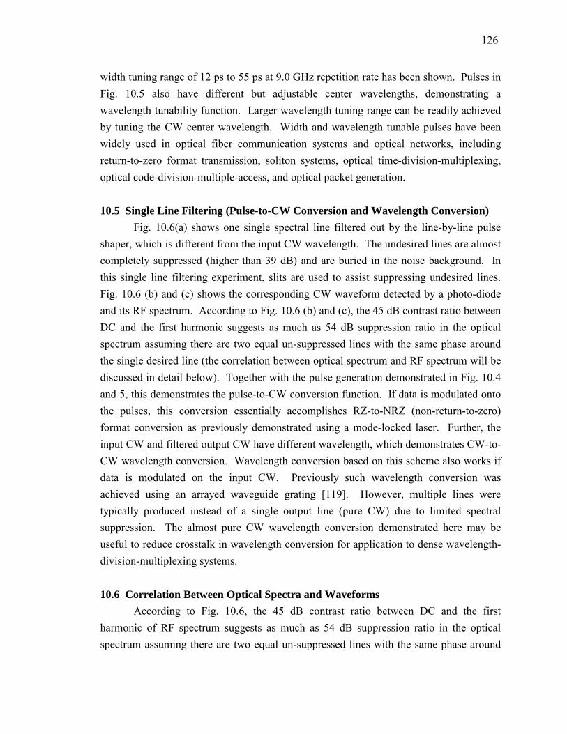
126
width tuning range of 12 ps to 55 ps at 9.0 GHz repetition rate has been shown. Pulses in Fig. 10.5 also have different but adjustable center wavelengths, demonstrating a wavelength tunability function. Larger wavelength tuning range can be readily achieved by tuning the CW center wavelength. Width and wavelength tunable pulses have been widely used in optical fiber communication systems and optical networks, including return-to-zero format transmission, soliton systems, optical time-division-multiplexing, optical code-division-multiple-access, and optical packet generation.
10.5 Single Line Filtering (Pulse-to-CW Conversion and Wavelength Conversion)
Fig. 10.6(a) shows one single spectral line filtered out by the line-by-line pulse shaper, which is different from the input CW wavelength. The undesired lines are almost completely suppressed (higher than 39 dB) and are buried in the noise background. In this single line filtering experiment, slits are used to assist suppressing undesired lines. Fig. 10.6 (b) and (c) shows the corresponding CW waveform detected by a photo-diode and its RF spectrum. According to Fig. 10.6 (b) and (c), the 45 dB contrast ratio between DC and the first harmonic suggests as much as 54 dB suppression ratio in the optical spectrum assuming there are two equal un-suppressed lines with the same phase around the single desired line (the correlation between optical spectrum and RF spectrum will be discussed in detail below). Together with the pulse generation demonstrated in Fig. 10.4 and 5, this demonstrates the pulse-to-CW conversion function. If data is modulated onto the pulses, this conversion essentially accomplishes RZ-to-NRZ (non-return-to-zero) format conversion as previously demonstrated using a mode-locked laser. Further, the input CW and filtered output CW have different wavelength, which demonstrates CW-to-CW wavelength conversion. Wavelength conversion based on this scheme also works if data is modulated on the input CW. Previously such wavelength conversion was achieved using an arrayed waveguide grating [119]. However, multiple lines were typically produced instead of a single output line (pure CW) due to limited spectral suppression. The almost pure CW wavelength conversion demonstrated here may be useful to reduce crosstalk in wavelength conversion for application to dense wavelength-division-multiplexing systems. 10.6 Correlation Between Optical Spectra and Waveforms
According to Fig. 10.6, the 45 dB contrast ratio between DC and the first harmonic of RF spectrum suggests as much as 54 dB suppression ratio in the optical spectrum assuming there are two equal un-suppressed lines with the same phase around
127
the single desired line. Reasonably good CW waveform in Fig. 10.6(b) is possible only because such high suppression ratio can be achieved. Even very slightly un-suppressed lines may introduce significant distortions, as shown in Fig. 10.7. Here two spectral lines are selected and one of them is intensity controlled with variable suppression ratio from -39 dB (shown in Fig. 10.6) to 0 dB. As little as a -29 dB lower un-suppressed spectral line distorts the �CW� waveforms visibly, in which the dots are measured results from the sampling scope and the solid curves are calculations based on two spectral lines (one desired, one partially suppressed). On the other hand, when the ratios of the two spectral lines approach 0 dB, the waveform changes are relatively small. The calculations and measurements agree well with each other. The valley of measured waveforms is higher than calculations, which is probably caused by the noise from optical amplifier. To understand these results, consider the field of two lines in the frequency domain, which can be expressed as
)exp()~()~()~( θδβδ jffffM −⋅∆−⋅+= (10.1)
where δ(⋅) represents the impulse function, β and θ represent the relative intensity and phase between the two spectral lines, and ∆f is the frequency spacing between two lines. The baseband frequency 0
~ fff −= , where f is optical frequency of spectral line and f0 is
some carrier frequency. In the time domain, the intensity profile can be obtained by Fourier Transform as
))2cos(21)( 2 θπββ −∆⋅++= fttm (10.2)
It is a cosine waveform with DC offset as expected. The ratio between peak-to-peak and mean value of the waveform is ( )ββ +14 , as shown in Fig. 10.8. When β is small, the
ratio is proportional to β4 , which suggests that a -20 dB un-suppressed line will cause
~40% variation on the waveform. When β is close to 0 dB, this ratio becomes saturated. The above analysis well explained the results in Fig. 10.7.
The key point is that extremely strong suppression of adjacent lines is required to extract a time-independent CW field from the mode-locked comb. This in turn suggests the need for pulse shaper spectral resolution much better than the spectral line spacing. Similar considerations are likely to prove at least equally important in line-by-line pulse shaping for generation of more complex waveforms made up of a multiplicity of lines.
10.7 Correlation Between Optical Spectra and RF Spectra
In the single spectral line filtering experiment shown in Fig. 10.6, the un-suppressed line is buried in the noise background of optical spectrum. A more sensitive

128
approach to monitor the suppression ratio is to measure the RF spectrum after opto-electro conversion. By comparing the DC and the first harmonic of the RF spectrum, the information of optical spectrum (such as the suppression ratio) can be deduced. This prompts us to investigate the correlation between optical spectra and RF spectra. For experimental convenience, the first and second harmonics of RF spectrum are compared but the principle can be applied to all other harmonics and DC.
Fig. 10.9(a) shows the selected 3 spectral lines with identical spectral phases and the corresponding calculated and measured RF spectrum (single-sided power spectrum). The relative intensities of these three lines are not intentionally controlled but rather arbitrarily set to show the general correlation between optical spectra and RF spectra. These three lines have identical phases directly after phase modulated CW (i.e., no additional spectral phase applied from LCM). Since there are three spectral lines, only the DC, the first and second harmonics for the RF spectrum show up. The RF spectrum can be calculated based on the intensity and phase information of the optical spectrum by the following procedure,
2
)(2
)~()~()()(
)()()(22
fIfItita
efAfAfAFFTIFFT
fiPhase
→ →→ →
→→ Φ
(10.3)
where A(f) is optical spectrum, Φ(f) is optical spectral phase, i(t) is the signal after opto-
electro conversion, and 2
)~( fI is the RF power spectrum. In our calculation the spectral
line intensities are measured values from OSA, and selected three spectral lines have identical spectral phases directly after the phase modulated CW. We don�t consider the distortion caused by the un-flat frequency response of the photo-diode, which is around ~1 dB within 20 GHz. The agreement between calculation and measurement is good. The discrepancy between them is mainly caused by the un-flat frequency response of the photo-diode and the possible contributions from un-suppressed adjacent lines other than those three selected lines. Fig. 10.9(b) shows the results for three lines with similar intensities but one line π phase shift controlled by the LCM. The RF spectrum changes largely and the first and second harmonics have almost equal powers. This shows the possibility to synthesize the RF spectrum by line-by-line pulse shaping on the intensity and phase of optical spectrum.
If we still select three lines, but control the outside two lines to have equal intensity, we have results shown in Fig. 10.10(a) with center line higher than outside lines and (b) with center line lower than outside lines. To simplify the study, we only focus on
129
the case in which these three lines have identical phases. Assuming the ratio of optical spectrum between outside lines and center line is r, the field of three lines with identical phases can be expressed as
)~()~()~()~( ffrffrffA ∆+⋅+∆−⋅+= δδδ (10.4)
After simple calculation using the procedure shown in eq. (3), the ratio of RF spectrum between the first and second harmonics is 4/r. This relationship is confirmed as shown in Fig. 10.10(c) by scanning the ratio of optical spectra using intensity control of pulse shaper. Note that since only ratios (or relative intensities) are measured in Fig. 10.10(c), we don�t need to use any adjustable parameters in theory to fit the measurements. Similarly, the ratio of RF spectrum between DC and first harmonic can be calculated as ( ) ( )rr 821 2+ , which reduces to ( )r81 when outside lines are small. Based
on this analysis, the 45 dB contrast ratio between DC and the first harmonic of RF spectrum in Fig. 10.6 suggests as much as 54 dB suppression ratio in the optical spectrum assuming there are two equal un-suppressed lines with the same phase around the single desired line. Note that in Fig. 10.6 the center line has a π phase shift relative to the outside two invisible lines, but the conclusion drawn here doesn�t change. Alternatively, if there is only one strong un-suppressed line in Fig. 10.6, as described by eq. (1), the ratio of RF spectrum between DC and first harmonic can be calculated as ( ) ( )ββ 21 2+ , which reduces to ( )β21 when un-suppressed line is small. Under this assumption, the
45 dB contrast ratio between DC and the first harmonic of RF spectrum in Fig. 10.6 suggests as much as 48 dB suppression ratio in the optical spectrum assuming there is only one strong un-suppressed line. 10.8 Microwave Waveform Synthesis
In this section, we select two lines with different separations to beat for microwave waveform synthesis, as shown in Fig. 10.11. The waveforms are generated after O/E conversion using a 50 GHz photo-diode, where 9 GHz, 18 GHz, 27 GHz, 36 GHz, 45 GHz, 54 GHz and 63 GHz waveforms are shown. The undesired spectral lines are well suppressed (higher than 34 dB suppression ratio, limited by the optical spectra measurements), making high purity microwave generation possible. The RF spectra measurements (up to 45 GHz waveform) show the harmonics suppression from 43 dB to 32 dB, depending on the frequencies of waveforms. Using similar procedure in section G and eq. (3), the optical spectra suppression ratio can be estimated according to RF spectrum harmonic suppression under certain assumptions. For example, in Fig. 10.11(a)
130
assuming that there are two equal un-suppressed lines around the two equal selected lines and all of them have identical phases, 43 dB RF harmonics suppression ratio suggests 52 dB optical spectrum suppression ratio. Note that other assumptions (for example, unequal un-suppressed lines or non-identical phases) will have somewhat different results. The noise of waveforms increases with the frequency of synthesized waveforms, which can be explained that two selected lines with larger separation have smaller powers and thus suffer from more noise from optical amplifier.
Only 9 GHz and its harmonics waveforms are synthesized in Fig. 10.11. Other frequencies and their harmonics can be readily generated by tuning the driving frequencies. For example, Fig. 10.12 shows two waveforms at 10.0 GHz and 13.5 GHz by driving the phase modulator appropriately and selecting two lines. In this way, almost any frequency supported by the bandwidth of generated spectral lines can be synthesized using only a ~10 GHz RF driving electronics. Optically generated microwave signals have the potential to impact fields such as ultra-wideband (UWB) wireless communications, impulsive radar and radio-over-fiber. 10.9 Spectral Line Fluctuation and Its Impact on Line-by-Line Pulse Shaping
Intuitively, full control of individual spectral lines requires frequency stabilized sources to generate stable spectral lines in addition to the high resolution pulse shapers to resolve and control individual spectral lines. Fig. 10.13 shows the relationship between spectral line stability and waveform noise process. Fig. 10.13(a) shows an overlap of multiple scans for the two spectral lines and sampling scope traces from our actively mode-locked fiber laser running at 10.5 GHz (not from the phase modulated CW), which shows observable frequency fluctuations. The cosine waveform is relatively clean if no phase shift is applied. However, if π phase shift is applied on one of the spectral lines the waveform shows time-dependent noise process, in which the noise in overlapped regime is more notable. These results have been clarified in chapter 6. In contrast, the phase modulated CW at 10.5 GHz in Fig. 10.13(b) shows spectral lines with reasonably good stability. The waveforms are clean for both 0 and π phase shift on one of the two spectra lines. The CW used in our experiments has a ~60 MHz fluctuation, which is sufficiently stable for those optical processing functionalities using line-by-line pulse shaping demonstrated in this paper. The simple comparison study in Fig. 10.13 shows the importance to have stable spectral lines for line-by-line pulse shaping.
In summary, we have demonstrated optical processing based on spectral line-by-line pulse shaping on a phase modulated CW laser and show various applications to fiber

131
communications including CW-to-pulse conversion, width and wavelength tunable return-to-zero pulse generation, pulse-to-CW conversion, wavelength conversion and application to microwave photonics. We also quantitatively studied the correlations between optical spectra, time domain waveforms and RF spectra. The phase modulated CW provides a simple but very flexible approach to generate spectral lines with reasonably good stability for line-by-line pulse shaping.
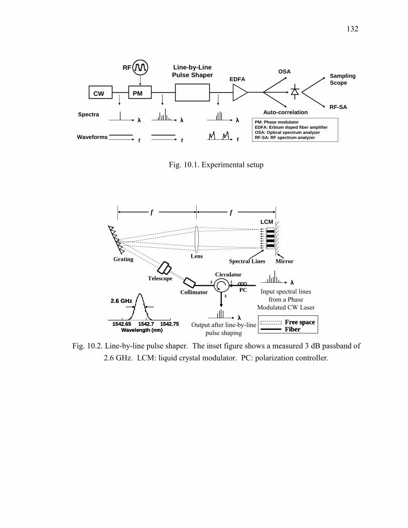
132
CW
Line-by-Line Pulse Shaper
PM
PM: Phase modulatorEDFA: Erbium doped fiber amplifierOSA: Optical spectrum analyzerRF-SA: RF spectrum analyzer
OSA
Auto-correlation
Sampling Scope
Spectra
Waveforms t
λλλλ
t
λλλλ λλλλ
t
EDFA
RF-SA
RF
Fig. 10.1. Experimental setup
MirrorGrating Lens
PCCollimator
Output after line-by-line pulse shaping
f f
Telescope
Free spaceFiberFree spaceFiber
2 1
3
Circulator
Input spectral lines from a Phase
Modulated CW Laser
Spectral Lines
LCM
λλλλ
λλλλ1542.65 1542.7 1542.75
Wavelength (nm)
2.6 GHz
1542.65 1542.7 1542.75Wavelength (nm)
2.6 GHz
Fig. 10.2. Line-by-line pulse shaper. The inset figure shows a measured 3 dB passband of
2.6 GHz. LCM: liquid crystal modulator. PC: polarization controller.

133
10 d
B/di
v
0-3-6
-8
+3
+6+7
1541.5 1542 1542.5 1543Wavelength (nm)
(a)
(b)
(c)
(d)
10 d
B/di
v
0-3-6
-8
+3
+6+7
0-3-6
-8
+3
+6+7
1541.5 1542 1542.5 1543Wavelength (nm)
(a)
(b)
(c)
(d)
Fig. 10.3. Spectra of (a) input CW (b) phase modulated CW at 9.0 GHz (c) phase
modulated CW at 9.0 GHz but tuning the input CW wavelength (d) phase modulated CW at 13.5 GHz.
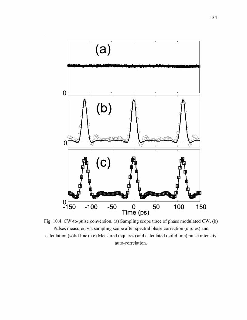
134
(a)
(b)
-150 -100 -50 0 50 100 150
(c)
Time (ps)
(a)
(b)
-150 -100 -50 0 50 100 150
(c)
Time (ps)0
0
0
Fig. 10.4. CW-to-pulse conversion. (a) Sampling scope trace of phase modulated CW. (b)
Pulses measured via sampling scope after spectral phase correction (circles) and calculation (solid line). (c) Measured (squares) and calculated (solid line) pulse intensity
auto-correlation.
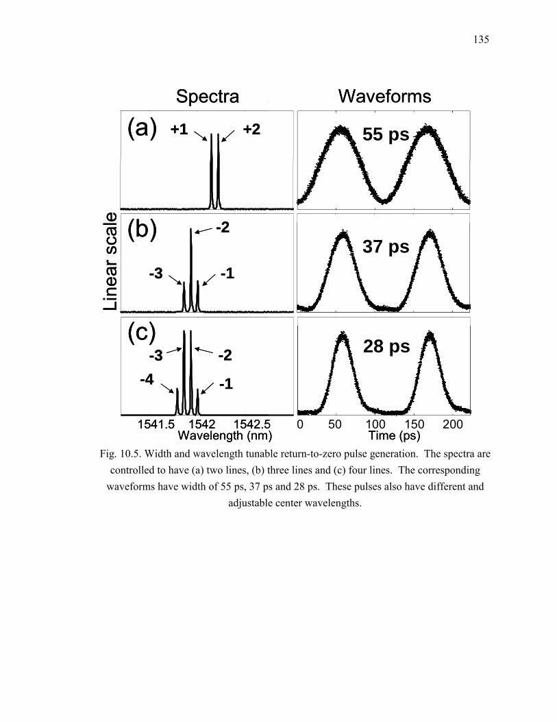
135
Line
ar s
cale
1541.5 1542 1542.5Wavelength (nm)
37 ps
28 ps
0 50 100 150 200Time (ps)
+2+1
-1-3
-2
-4-2
-1
-3
(a)
(b)
(c)
55 ps
Spectra WaveformsLi
near
sca
le
1541.5 1542 1542.5Wavelength (nm)
37 ps
28 ps
0 50 100 150 200Time (ps)
+2+1
-1-3
-2
-4-2
-1
-3
(a)
(b)
(c)
55 ps
Spectra Waveforms
Fig. 10.5. Width and wavelength tunable return-to-zero pulse generation. The spectra are
controlled to have (a) two lines, (b) three lines and (c) four lines. The corresponding waveforms have width of 55 ps, 37 ps and 28 ps. These pulses also have different and
adjustable center wavelengths.

136
-150 -100 -50 0 50 100 150
150
0
1541.5 1542 1542.5 1543Wavelength (nm)
10 d
B/d
iv
+1
0 +2 -39 dB
-11 dBm
-56 dBm
(a)
(b)
(c)
0 10 20 30 40 50
-80
-60
-40
-20
Frequency (GHz)
Pow
er (d
Bm
)
Time (ps)
Vol
tage
(mV
)
Original CW position
-150 -100 -50 0 50 100 150-150 -100 -50 0 50 100 150
150
0
1541.5 1542 1542.5 1543Wavelength (nm)
10 d
B/d
iv
+1
0 +2 -39 dB
-11 dBm
-56 dBm
(a)
(b)
(c)
0 10 20 30 40 50
-80
-60
-40
-20
Frequency (GHz)
Pow
er (d
Bm
)
Time (ps)
Vol
tage
(mV
)
Original CW position
Fig. 10.6. Pulse-to-CW conversion and CW-to-CW wavelength conversion. (a) Optical
spectrum of one filtered line, which is different from the input CW wavelength. (b) Corresponding CW waveform detected by a photo-diode and (c) RF spectrum.
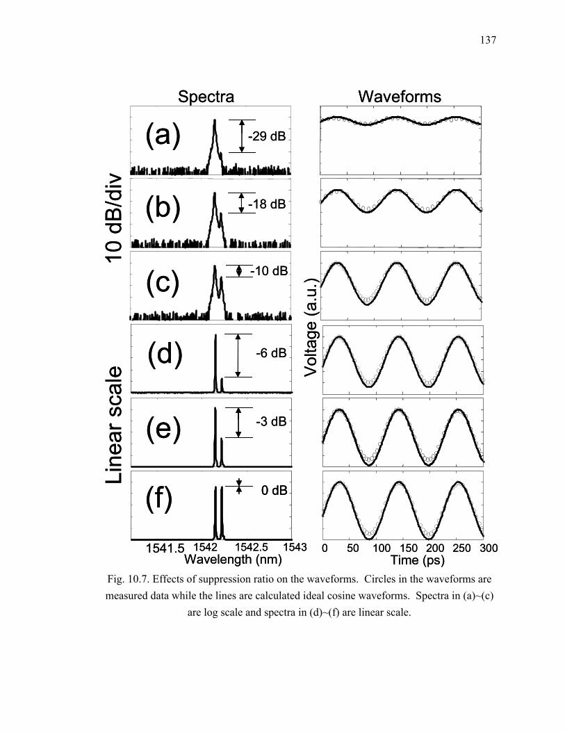
137
-29 dB
-18 dB
-10 dB
Vol
tage
(a.u
.)
Spectra Waveforms
-6 dB
1541.5 1542 1542.5 1543Wavelength (nm)
0 50 100 150 200 250 300
-3 dB
0 dB
Time (ps)
(a)
(b)
(c)
(d)
(e)
(f)
Line
ar s
cale
10 d
B/d
iv-29 dB
-18 dB
-10 dB
Vol
tage
(a.u
.)
Spectra Waveforms
-6 dB
1541.5 1542 1542.5 1543Wavelength (nm)
0 50 100 150 200 250 300
-3 dB
0 dB0 dB
Time (ps)
(a)
(b)
(c)
(d)
(e)
(f)
Line
ar s
cale
10 d
B/d
iv
Fig. 10.7. Effects of suppression ratio on the waveforms. Circles in the waveforms are measured data while the lines are calculated ideal cosine waveforms. Spectra in (a)~(c)
are log scale and spectra in (d)~(f) are linear scale.

138
-40 -30 -20 -10 0-15
-10
-5
0
5
Ratio between two spectral lines β
Rat
io b
etw
een
peak
-pea
k an
d m
ean
MeasurementTheory
-40 -30 -20 -10 0-15
-10
-5
0
5
Ratio between two spectral lines β
Rat
io b
etw
een
peak
-pea
k an
d m
ean
MeasurementTheory
Fig. 10.8. Correlation between optical spectra and waveforms for two spectral lines.
-70-60-50-40-30-20-10
Pow
er (d
Bm
)
13.2 dB12.3 dB
10 d
B/d
iv
Phase: 0 0 0
10 d
B/d
iv
1541.5 1542 1542.5Wavelength (nm)
Phase: 0 0 π
0 10 20 30 40 50
-0.1 dB
0 10 20 30 40 50
-70-60-50-40-30-20-10
Frequency (GHz)
1.5 dB
Frequency (GHz)
Optical Spectra Calculated RF Spectra Measured RF Spectra
(a)
(b)
-70-60-50-40-30-20-10
Pow
er (d
Bm
)
13.2 dB12.3 dB
10 d
B/d
iv
Phase: 0 0 0Phase: 0 0 0
10 d
B/d
iv
1541.5 1542 1542.5Wavelength (nm)
1541.5 1542 1542.5Wavelength (nm)
Phase: 0 0 π
0 10 20 30 40 50
-0.1 dB
0 10 20 30 40 50
-70-60-50-40-30-20-10
Frequency (GHz)
1.5 dB
Frequency (GHz)
Optical Spectra Calculated RF Spectra Measured RF Spectra
(a)
(b)
Fig. 10.9. Correlation between optical spectra and RF spectra for three spectral lines. (a)
Three lines with identical phases. (b) Three lines with one line π phase shift.

139
10 d
B/d
iv
1541.5 1542 1542.5Wavelength (nm)
0 10 20 30 40 50Frequency (GHz)
8.2 dB-2.3dB
-10.2 dB 17.3 dB
10 d
B/d
iv
(a)
(b)
Optical Spectra Measured RF Spectra
Optical spectra contrast ratio (dB)
RF
spec
tra c
ontra
st ra
tio (d
B)
-30 -20 -10 0 10 20 30
-20
-10
0
10
20
30
40(c) Correlation between optical spectra and RF spectra
MeasurementTheory
10 d
B/d
iv
1541.5 1542 1542.5Wavelength (nm)
0 10 20 30 40 50Frequency (GHz)
8.2 dB-2.3dB
-10.2 dB-10.2 dB 17.3 dB
10 d
B/d
iv
(a)
(b)
Optical Spectra Measured RF Spectra
Optical spectra contrast ratio (dB)
RF
spec
tra c
ontra
st ra
tio (d
B)
-30 -20 -10 0 10 20 30
-20
-10
0
10
20
30
40
-30 -20 -10 0 10 20 30
-20
-10
0
10
20
30
40(c) Correlation between optical spectra and RF spectra
MeasurementTheory
Fig. 10.10. Correlation between optical spectra and RF spectra for three spectral lines with identical phases, where the two outside lines are controlled to have equal intensity. (a) Center line higher than outside lines. (b) Center line lower than outside lines. (c) RF
spectra contrast ratio versus optical spectra contrast ratio.
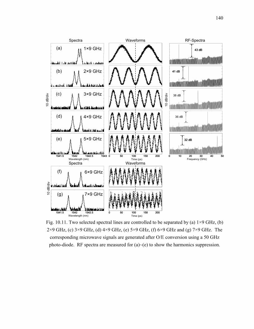
140
(a) 43 dB43 dB10
dB
/div
10 d
B/d
iv
41 dB41 dB
36 dB
Wavelength (nm) Frequency (GHz)0 10 20 30 40 50
32 dB
0 10 20 30 40 50
32 dB
1541.5 1542 1542.5 15431541.5 1542 1542.5 1543 0 50 100 150 2000 50 100 150 200
Spectra Waveforms RF-Spectra
Time (ps)
(b)
(c)
(d)
(e)
1×9 GHz
2×9 GHz
3×9 GHz
4×9 GHz
5×9 GHz
38 dB
(f)
(g)
6×9 GHz
7×9 GHz
1541.5 1542 1542.51541.5 1542 1542.5Wavelength (nm)
10 d
B/d
iv
0 50 100 150 2000 50 100 150 200Time (ps)
Spectra Waveforms
Fig. 10.11. Two selected spectral lines are controlled to be separated by (a) 1×9 GHz, (b) 2×9 GHz, (c) 3×9 GHz, (d) 4×9 GHz, (e) 5×9 GHz, (f) 6×9 GHz and (g) 7×9 GHz. The
corresponding microwave signals are generated after O/E conversion using a 50 GHz photo-diode. RF spectra are measured for (a)~(e) to show the harmonics suppression.
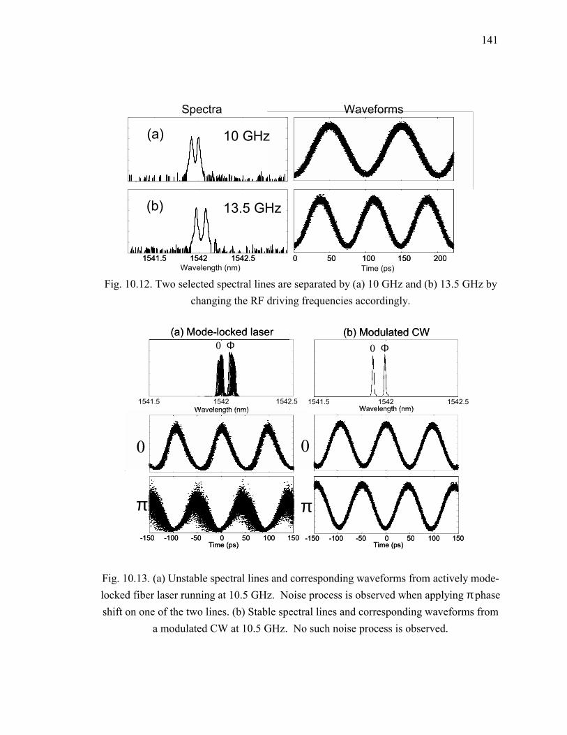
141
(a)
(b)
10 GHz
13.5 GHz
Wavelength (nm)0 50 100 150 2000 50 100 150 200
Time (ps)
Spectra Waveforms
1541.5 1542 1542.51541.5 1542 1542.5
Fig. 10.12. Two selected spectral lines are separated by (a) 10 GHz and (b) 13.5 GHz by changing the RF driving frequencies accordingly.
1541.5 1542 1542.5 1541.5 1542 1542.5
-150 -100 -50 0 50 100 150
Wavelength (nm)Wavelength (nm)
Time (ps)Time (ps)
0
π
0
0 Φ0 Φ
-150 -100 -50 0 50 100 150
(b) Modulated CW(a) Mode-locked laser
π
1541.5 1542 1542.5 1541.5 1542 1542.5
-150 -100 -50 0 50 100 150-150 -100 -50 0 50 100 150
Wavelength (nm)Wavelength (nm)
Time (ps)Time (ps)
0
π
0
0 Φ0 Φ
-150 -100 -50 0 50 100 150-150 -100 -50 0 50 100 150
(b) Modulated CW(a) Mode-locked laser
π
Fig. 10.13. (a) Unstable spectral lines and corresponding waveforms from actively mode-locked fiber laser running at 10.5 GHz. Noise process is observed when applying π phase shift on one of the two lines. (b) Stable spectral lines and corresponding waveforms from
a modulated CW at 10.5 GHz. No such noise process is observed.
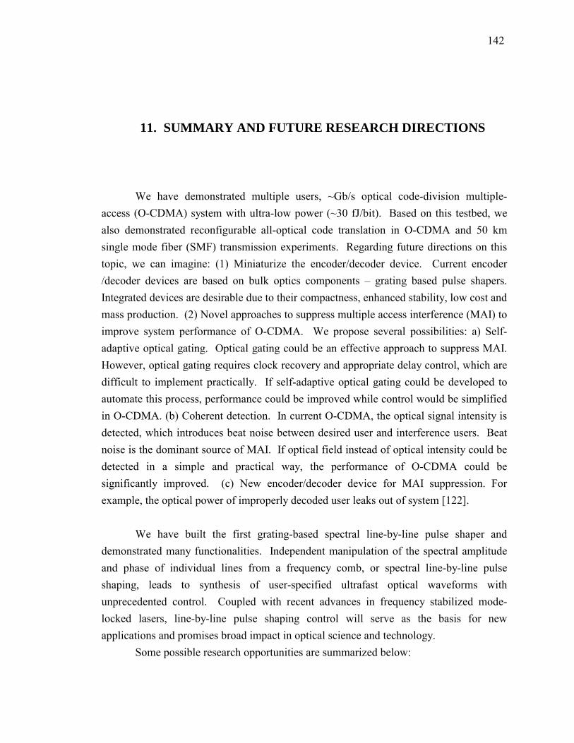
142
11. SUMMARY AND FUTURE RESEARCH DIRECTIONS
We have demonstrated multiple users, ~Gb/s optical code-division multiple-
access (O-CDMA) system with ultra-low power (~30 fJ/bit). Based on this testbed, we also demonstrated reconfigurable all-optical code translation in O-CDMA and 50 km single mode fiber (SMF) transmission experiments. Regarding future directions on this topic, we can imagine: (1) Miniaturize the encoder/decoder device. Current encoder /decoder devices are based on bulk optics components � grating based pulse shapers. Integrated devices are desirable due to their compactness, enhanced stability, low cost and mass production. (2) Novel approaches to suppress multiple access interference (MAI) to improve system performance of O-CDMA. We propose several possibilities: a) Self-adaptive optical gating. Optical gating could be an effective approach to suppress MAI. However, optical gating requires clock recovery and appropriate delay control, which are difficult to implement practically. If self-adaptive optical gating could be developed to automate this process, performance could be improved while control would be simplified in O-CDMA. (b) Coherent detection. In current O-CDMA, the optical signal intensity is detected, which introduces beat noise between desired user and interference users. Beat noise is the dominant source of MAI. If optical field instead of optical intensity could be detected in a simple and practical way, the performance of O-CDMA could be significantly improved. (c) New encoder/decoder device for MAI suppression. For example, the optical power of improperly decoded user leaks out of system [122].
We have built the first grating-based spectral line-by-line pulse shaper and
demonstrated many functionalities. Independent manipulation of the spectral amplitude and phase of individual lines from a frequency comb, or spectral line-by-line pulse shaping, leads to synthesis of user-specified ultrafast optical waveforms with unprecedented control. Coupled with recent advances in frequency stabilized mode-locked lasers, line-by-line pulse shaping control will serve as the basis for new applications and promises broad impact in optical science and technology.
Some possible research opportunities are summarized below:

143
• In the current experiments we performed line-by-line pulse shaping control for optical arbitrary waveform generation (O-AWG) relying only on sufficient passive spectral line stability of the mode-locked laser. We can anticipate further progress by performing similar line-by-line shaping experiments on state-of-the-art frequency-stabilized mode-locked sources, which will provide substantial advantages in long-term coherence.
• Current experiments are performed based on 3 ps or 400 fs pulses. Also of interest is to extend the optical bandwidth which is shaped to beyond 100 THz, a bandwidth already available from mode-locked lasers. This will require new modulator arrays with at least tens of thousands of pixels, a number which is well beyond current arrays specifically configured for pulse shaping (pixel counts up to 640 have been demonstrated in LCMs [123, 124], with similar level of control available from acousto-optic modulators [125]). Development of such large pulse shaping arrays should be plausible in view of the similarity to large array technologies that have been highly developed for computer displays. Once such large pulse shaping arrays are available, we can immediately pursue: (1) complex arbitrary waveform generation with high fidelity; (2) shorter pulse generation using line-by-line pulse shaping on a phase modulated CW laser with a broader bandwidth.
• Although various applications based on line-by-line pulse shaping have been shown in our work, more are expected. As an example, we could extend the approach for microwave generation to the regime of Terahertz (THz). This could be a powerful tool to synthesize THz waveforms. We also need to think of the applications for O-AWG: when and where do we really need the complex arbitrary waveforms based on broadband line-by-line pulse shaping?
• Finally, pulse shaping experiments to date, including those reported here, are generally constrained to generate waveforms periodic at the repetition rate of the mode-locked laser source. However, by fabricating optoelectronic or electro-optic modulator arrays which are in principle capable of being reprogrammed deep into the subnanosecond range, in the future it should be possible to change on subsequent mode-locked pulses to independent new waveform shapes, which could be stitched coherently together to yield arbitrary optical waveforms of unlimited length. This pulse-by-pulse pattern update can also be analyzed in frequency domain. Each spectral line is modulated like a CW by the pattern at repetition rate and thus is broadened. All the broadened spectral lines overlap

144
with each other and add together coherently, which may show some new features beyond previous observations. This problem should be investigated at least theoretically even the apparatus is currently not available.

LIST OF REFERENCES
145
LIST OF REFERENCES [1] A. H. Gnauck et al., �6 x 42.7 Gb/s transmission over ten 200 km EDFA-amplified
SSMF spans using polarization-alternating RZ-DPSK,” in 2004 Proc. Conf. Optic. Fiber Commun.(OFC’04), Postdeadline paper PDP35, Los Angeles, CA, 2004.
[2] G. Charlet et al., �WDM transmission at 6 Tbit/s capacity over transatlantic distance, using 42.7Gb/s Differential Phase-Shift Keying without pulse carver,” in 2004 Proc. Conf. Optic. Fiber Commun.(OFC’04), Postdeadline paper PDP36, Los Angeles, CA, 2004.
[3] L. Becouarn et al., �42 x 42.7 Gb/s RZ-DPSK transmission over a 4820 km long NZDSF deployed line using C-band-only EDFAs,” in 2004 Proc. Conf. Optic. Fiber Commun.(OFC’04), Postdeadline paper PDP37, Los Angeles, CA, 2004.
[4] N. Yoshikane et al., �1.14 b/s/Hz spectrally-efficient 50 x 85.4 Gb/s transmission over 300 km using copolarized CS-RZ DQPSK signals,” in 2004 Proc. Conf. Optic. Fiber Commun.(OFC’04), Postdeadline paper PDP38, Los Angeles, CA, 2004.
[5] J. P. Turkiewicz et al., �Field trial of 160Gbit/s OTDM add/drop node in a link of 275 km deployed fiber,” in 2004 Proc. Conf. Optic. Fiber Commun.(OFC’04), Postdeadline paper PDP1, Los Angeles, CA, 2004.
[6] T. Ohara, H. Takara, I. Shake, K. Mori, K. Sato, S. Kawanishi, S. Mino, I. Yamada, A. Ishii, I. Ogawa, T. Kitoh, K. Magari, A. Okamoto, R. V. Roussev, J. R. Kurz, K. R. Parameswaran, M. M. Fejer, �160-Gb/s OTDM transmission using integrated all-optical MUX/DEMUX with all-channel modulation and demultiplexing,� IEEE Photon. Technol. Lett., vol. 16, pp. 650-652, Feb. 2004.
[7] J. Shah, �Optical CDMA,� Optics & Photonics News., vol. 14, pp. 42-47, Apr. 2003. [8] D. D. Sampson, G. J. Pendock, and R. A. Griffin, �Photonic code division multiple
access communications,� Fiber Integrated Opt., vol. 16, pp. 129-157, 1997. [9] A. M. Weiner, and J. A. Salehi, �Optical code-division multiple access,� in Photonics
in Switching, J. E. Midwinter, Ed. San Diego, CA: Academic, vol. 2, pp. 73-118, 1993.
[10] J. A. Salehi, A. M. Weiner, and J. P. Heritage, �Coherent ultrashort light pulse code-division multiple access communication systems,� J. Lightwave Technol., vol. 8, pp. 478-491, Mar. 1990.
[11] R. Papannareddy and A. M. Weiner, �Performance comparison of coherent ultrashort light pulse and incoherent broad-band CDMA systems,� IEEE Photon. Technol. Lett., vol. 11, pp. 1683-1685, Dec. 1999.
146
[12] P. R. Prucnal, M. A. Santoro, and T. R. Fan, �Spread spectrum fiber-optic local area network using optical processing,� J. Lightwave Technol., vol. 4, pp. 547-554, May 1986.
[13] R. A. Griffin, D. D. Sampson, and D. A. Jackson, �Coherence coding for photonic code-division multiple access networks,� J. Lightwave Technol., vol. 13, pp. 1826-1837, Sep. 1995.
[14] D. Zaccarin and M. Kavehrad, �An optical CDMA system based on spectral encoding of LED,� IEEE Photon. Technol. Lett., vol. 5, pp. 479-482, Apr. 1993.
[15] H. P. Sardesai, C.-C. Chang, and A. M. Weiner, �A femtosecond code division multiple access communication system test-bed,� J. Lightwave Technol., vol. 16, pp. 1953-1964, Nov. 1998.
[16] S. Shen, A. M. Weiner, and G. D. Sucha, �Bit error rate performance of ultrashort-pulse optical CDMA detection under multi-access interference,� Electron. Lett., vol. 36, pp. 1795-1797, Oct. 2000.
[17] S. Shen and A. M. Weiner, �Suppression of WDM interference for error-free detection of ultrashort-pulse CDMA signals in a hybrid optical WDM-CDMA system,� IEEE Photon. Technol. Lett., vol. 13, pp. 82-84, Jan. 2001.
[18] H. Tsuda, H. Takenouchi, T. Ishii T, K. Okamoto, T. Goh, K. Sato, A. Hirano, T. Kurokawa, C. Amano, �Spectral encoding and decoding of 10 Gbit/s femtosecond pulses using high resolution arrayed-waveguide grating,� Electron. Lett., vol. 35, pp. 1186-1188, July 1999.
[19] N. Wada, K. Kitayama, �A 10 Gb/s optical code division multiplexing using 8-chip optical bipolar code and coherent detection,� J. Lightwave Technol., vol. 17, pp. 1758-1765, Oct. 1999.
[20] H. Sotobayashi, W. Chujo, and K. Kitayama, �1.6-b/s/Hz 6.4-Tb/s QPSK-OCDMA/WDM (4 OCDMA x 40 WDM x 40 Gb/s) transmission experiment using optical hard thresholding,� IEEE Photon. Technol. Lett., vol. 14, pp. 555-557, Apr. 2002.
[21] H. Sotobayashi, W. Chujo, and K. Kitayama, "Highly spectral-efficient optical code-division multiplexing transmission system," IEEE J. Select. Topics Quantum Electron., vol. 10, pp. 250-258, Mar./Apr. 2004.
[22] S. Kutsuzawa, N. Minato, S. Oshiba, A. Nishiki, K. Kitayama, �10 Gb/s, x 2 ch signal unrepeated transmission over 100 km of data rate enhanced time-spread/wavelength-hopping OCDM using 2.5-Gb/s-FBG en/decoder,� IEEE Photon. Technol. Lett., vol. 15, pp. 317-319, Feb. 2003.
[23] M. R. Mokhtar, M. Ibsen, P. C. Teh, D. J. Richardson, �Reconfigurable multilevel phase-shift keying encoder-decoder for all-optical networks,� IEEE Photon. Technol. Lett., vol. 15, pp. 431-433, Mar 2003.
[24] P. C. Teh, M. Ibsen, D. J. Richardson, �Demonstration of a full-duplex bidirectional spectrally interleaved OCDMA/DWDM system,� IEEE Photon. Technol. Lett., vol. 15, pp. 482-484, Mar 2003.

147
[25] J. H. Lee, P. C. Teh, Z. Yusoff, M. Ibsen, W. Belardi, T. M. Monro, D. J. Richardson, �A holey fiber-based nonlinear thresholding device for optical CDMA receiver performance enhancement,� IEEE Photon. Technol. Lett., vol. 14, pp. 876-878, June 2002.
[26] P. C. Teh, M. Ibsen, J. H. Lee, P. Petropoulos, D. J. Richardson, �Demonstration of a four-channel WDM/OCDMA system using 255-chip 320-Gchip/s quarternary phase coding gratings,� IEEE Photon. Technol. Lett., vol. 14, pp. 227-229, Feb. 2002.
[27] P. Petropoulos, N. Wada, P. C. Teh, M. Ibsen, W. Chujo, K. Kitayama, D. J. Richardson, �Demonstration of a 64-chip OCDMA system using superstructured fiber gratings and time-gating detection,� IEEE Photon. Technol. Lett., vol. 13, 1239-1241, Nov. 2001.
[28] A. Grunnet-Jepsen , A. E. Johnson, E. S. Maniloff, T. W. Mossberg, M. J. Munroe, J. N. Sweetser, �Fibre Bragg grating based spectral encoder/decoder for lightwave CDMA,� Electron. Lett., vol. 35, pp. 1096-1097, June 1999.
[29] A. Grunnet-Jepsen, A. E. Johnson, E. S. Maniloff, T. W. Mossberg, M. J. Munroe, J. N. Sweetser, �Demonstration of all-fiber sparse lightwave CDMA based on temporal phase encoding,� IEEE Photon. Technol. Lett., vol. 11, pp. 1283-1285, Oct. 1999.
[30] D. Gurkan, S. Kumar, A. Sahin, A. Willner, K. Parameswaran, M. Fejer, D. Starodubov, J. Bannister, P. Kamath, J. Touch, �All-optical wavelength and time 2-D code converter for dynamically-reconfigurable O-CDMA Neteworks using a PPLN waveguide,� in 2003 Proc. Conf. Optic. Fiber Commun.(OFC’03), FD6, Atlanta, Georgia, 2003.
[31] J. E. McGeehan, S. M. Reza, M. Nezam, P. Saghari, A. E. Willner, R. Omrani, V. Kumar, �3D time-wavelength-polarization OCDMA coding for increasing the number of users in OCDMA LANs,� in 2004 Proc. Conf. Optic. Fiber Commun.(OFC’04), FE5, Los Angeles, CA, 2004.
[32] S. Etemad, T. Banwell, S. Galli, J. Jackel, R. Menendez, P. Toliver, J. Young, P. Delfyett, C. Price, T. Turpin, �Optical-CDMA incorporating phase coding of coherent frequency bins: concept, simulation, experiment,� in 2004 Proc. Conf. Optic. Fiber Commun.(OFC’04), FG 5, Los Angeles, CA, 2004.
[33] K. Li, W. Cong, V. J. Hernandez, R. P. Scott, J. Cao, Y. Du, J. P. Heritage, B. H. Kolner, and S. J. B. Yoo, �10 Gbit/s optical CDMA encoder-decoder BER performance using HNLF thresholder,� in 2004 Proc. Conf. Optic. Fiber Commun.(OFC’04), MF 87, Los Angeles, CA, 2004.
[34] Z. Jiang, D. S. Seo, S.-D. Yang, , D. E. Leaird, A. M. Weiner, R. V. Roussev, C. Langrock, and M. M. Fejer, �Four user, 2.5 Gb/s, spectrally coded O-CDMA system demonstration using low power nonlinear processing,� in 2004 Proc. Conf. Optic. Fiber Commun.(OFC’04), PDP29, Los Angeles, CA, 2004; �Spectrally coded O-CDMA system with four users at 2.5 Gbit/s using low power nonlinear processing,� Electron. Lett., vol. 40, pp. 623- 625, May 2004.
[35] R. L. Peterson, R. E. Ziemer, D. E. Borth, Introduction to spread-spectrum communications, Englewood Cliffs, NJ : Prentice Hall, 1995.

148
[36] J. G. Proakis, Digital Communications, 3rd ed. McGraw-Hill, New York, 1995. [37] S. Etemad, P. Toliver, R. Menendez, J. Young, T. Banwell, S. Galli, J. Jackel, P.
Delfyett, C. Price, and T. Turpin, �Spectrally efficient optical CDMA using coherent phase-frequency coding,� IEEE Photon. Technol. Lett., vol. 17, no. 4, pp. 929-931, April 2005.
[38] A. Agarwal, P. Toliver, R. Menendez, et al., �Fully programmable ring-resonator-based integrated photonic circuit for phase coherent applications,� J. Lightwave Technol., vol. 24, no. 1, pp. 77-87, Jan 2006.
[39] V. Baby, I. Glesk, R. J. Runser, R. Fischer, Y. K. Huang, C. S. Bres, W. C. Kwong, T. H. Curtis, and P. R. Prucnal, �Experimental demonstration and scalability analysis of a four-node 102-Gchip/s fast frequency-hopping time-spreading optical CDMA network,� IEEE Photonics Technol. Lett., vol. 17, no. 1, pp. 253-255, Jan. 2005.
[40] V. J. Hernandez, W. Cong, R. P. Scott, C. Yang, N. K. Fontaine, B. H. Kolner, J. P. Heritage, S. J. Ben Yoo, �320-Gb/s Capacity (32 Users × 10 Gb/s) SPECTS O-CDMA Local Area Network Testbed,� in 2006 Optical Fiber Communications Conference (OFC2006), PDP45, Anaheim, CA, March 5-10, 2006.
[41] R. P. Scott, W. Cong, V. J. Hernandez, K. B. Li, B. H. Kolner, J. P. Heritage, and S. J. B. Yoo, �An eight-user time-slotted SPECTS O-CDMA testbed: Demonstration and simulations,� J. Lightwave Technol., vol. 23, no. 10, pp. 3232-3240, Oct. 2005.
[42] P. C. Teh, M. Ibsen, J. H. Lee, P. Petropoulos, and D. J. Richardson, �Demonstration of a four-channel WDM/OCDMA system using 255-chip 320-Gchips/s quaternary phase coding gratings,� IEEE Photonics Technol. Lett., vol. 14, no. 2, pp. 227-229, Feb. 2002.
[43] H. Sotobayashi, W. Chujo, K. Kitayama, �Highly spectral-efficient optical code-division multiplexing transmission system,� IEEE J. Select. Topics Quantum Electron., vol. 10, no. 2, pp. 250-258, 2004.
[44] X. Wang, N. Wada, T. Hamanaka, K. Kitayama, and A. Nishiki, �10-user, truly-asynchronous OCDMA experiment with 511-chip SSFBG en/decoder and SC-based optical thresholder,� in the 2005 Optical Fiber Communication Conf. (OFC’05), Anaheim, CA, paper PDP33, 2005.
[45] X. Wang, N. Wada, T. Miyazaki, G. Cincotti, K. Kitayama, �Field Trial of 3-WDM×10-OCDMA×10.71 Gbps, Truly-Asynchronous, WDM/DPSK-OCDMA Using Hybrid E/D without FEC and Optical Threshold,� in 2006 Optical Fiber Communications Conference (OFC2006), PDP44, Anaheim, CA, March 5-10, 2006.
[46] S. T. Cundiff, �Phase stabilization of ultrashort optical pulses,� J. Phys. D, vol. 35, no. 8, R43-R59, April 2002.
[47] A. M. Weiner, �Femtosecond pulse shaping using spatial light modulators,� Rev. Sci. Instr., vol. 71, pp. 1929-1960, May 2000.
[48] D. J. Jones, S. A. Diddams, J. K. Ranka, A. Stentz, R. S. Windeler, J. L. Hall, S. T. Cundiff, �Carrier-envelope phase control of femtosecond mode-locked lasers and direct optical frequency synthesis,� Science, vol. 288, pp. 635-639, April 2000.
[49] T. Udem, R. Holzwarth, T. W. Hansch, �Optical frequency metrology,� Nature, vol. 416, pp. 233-237, March 2002.

149
[50] Z. Jiang, D. S. Seo, D. E. Leaird, A. M. Weiner, �Spectral line-by-line pulse shaping,� Optics Lett., vol. 30, no. 12, pp. 1557-1559, June, 2005.
[51] S. Etemad, T. Banwell, S. Galli, J. Jackel, R. Menendez, P. Toliver, J. Young, P. Delfyett, C. Price, and T. Turpin, �Optical-CDMA incorporating phase coding of coherent frequency bins: concept, simulation, experiment,� in 2004 Optical Fiber Conf. (OFC2004), FG5, Los Angeles, CA, 2004.
[52] T. Yilmaz, C. M. DePriest, T. Turpin, J. H. Abeles, and P. J. Delfyett, �Toward a photonic arbitrary waveform generator using a modelocked external cavity semiconductor laser,� IEEE Photon. Technol. Lett., vol. 14, no. 11, pp. 1608-1610, Nov. 2002.
[53] Z. Jiang, D. S. Seo, S.-D. Yang, D. E. Leaird, A. M. Weiner, R. V. Roussev, C. Langrock, and M. M. Fejer, �Four user, 2.5 Gb/s, spectrally coded O-CDMA system demonstration using low power nonlinear processing,� J. Lightwave Technol., vol. 23, pp. 143-158, Jan. 2005.
[54] Z. Jiang, D. S. Seo, S.-D. Yang, D. E. Leaird, A. M. Weiner, R. V. Roussev, C. Langrock, and M. M. Fejer, �Four user, 10 Gb/s spectrally phase coded O-CDMA system operating at ~30 fJ/bit,� IEEE Photon. Technol. Lett., vol. 17, pp. 705-707, Mar. 2005.
[55] Z. Jiang, D. S. Seo, D. E. Leaird, A. M. Weiner, R. V. Roussev, C. Langrock, and M. M. Fejer, �Multi-user, 10 Gb/s spectrally phase coded O-CDMA system with hybrid chip and slot-level timing coordination,� IEICE Electron. Express, vol. 1, pp. 398-403, Oct. 2004.
[56] A. M. Weiner, J. P. Heritage, and E. M. Kirchner, �High resolution femtosecond pulse shaping,� J. Opt. Soc. Amer., vol. B5, pp. 1563-1572, Aug. 1988.
[57] A. M. Weiner, D. E. Leaird, J. S. Patel, and J. R. Wullert, �Programmable shaping of femtosecond optical pulses by use of a 128-element liquid crystal phase modulator,� IEEE J. Quantum. Electron., vol. 28, pp. 908-920, Apr. 1992.
[58] D. S. Seo, D. E. Leaird, A. M. Weiner, S. Kamei, M. Ishii, A. Sugita, K. Okamoto, �Continuous 500 GHz pulse train generation by repetition-rate multiplication using arrayed waveguide grating,� Electron. Lett., vol. 39, pp. 1138-1140, July 2003.
[59] R. Nelson, D. E. Leaird, and A. M. Weiner, �Programmable polarization-independent spectral phase compensation and pulse shaping,� Opt. Exp., vol. 11, pp. 1763-1769, July 2003.
[60] R. N. Thurston, J. P. Heritage, A. M. Weiner and W. J. Tomlinson, �Analysis of picosecond pulse shape synthesis by spectral masking in a grating pulse compressor,� IEEE J. Quantum. Electron., vol. 22, pp. 682-696, May 1986.
[61] K. R. Parameswaran, R. K. Route, J. R. Kurz, R. V. Roussev, M. M. Fejer, M. Fujimura, �Highly efficient second-harmonic generation in buried waveguides formed by annealed and reverse proton exchange in periodically poled lithium niobate,� Opt. Lett., vol. 27, pp. 179-181, Feb. 2002.
[62] Z. Zheng and A. M. Weiner, �Spectral phase correlation of coded femtosecond pulses by second-harmonic generation in thick nonlinear crystals,� Opt. Lett., vol. 25, pp. 984-986, July 2000.
150
[63] Z. Zheng, A. M. Weiner, K. R. Parameswaran, M. H. Chou, and M. M. Fejer, �Low power spectral phase correlator using periodically poled LiNbO3 waveguides,� IEEE Photon. Technol. Lett., vol. 4, pp. 376-378, Apr. 2001.
[64] Z. Jiang, D. S. Seo, S.-D. Yang, D. E. Leaird, A. M. Weiner, R. V. Roussev, C. Langrock, and M. M. Fejer, �Low power, high-contrast coded waveform discrimination at 10 GHz via nonlinear processing,� IEEE Photon. Technol. Lett., vol. 16, pp. 1778-1780, July 2004.
[65] S. Boztas, R. Hammons, P.V. Kumar, �4-phase sequences with near-optimum correlation properties,� IEEE Trans. Inform. Theory, vol. 38, pp. 1101-1113, May 1992.
[66] M. R. Schroeder, Number theory in science and communication, Chap. 15, Springer-Verlag, 1985.
[67] F. Forghieri, P. R. Prucnal, R. W. Tkach, and A. R. Chraplyvy, �RZ versus NRZ in nonlinear WDM systems,� IEEE Photon. Technol. Lett., vol. 9, pp. 1035-1037, July 1997.
[68] Z. Jiang, D. S. Seo, D. E. Leaird, A. M. Weiner, R. V. Roussev, C. Langrock, and M. M. Fejer, �Reconfigurable All-Optical Code Translation in Spectrally Phase Coded O-CDMA,� J. Lightwave Technol., vol. 23, no. 6, pp. 1979-1990, June 2005.
[69] R. Ramaswami and K. N. Sivarajan, Optical networks: A Practical Perspective, Morgan Kaufmann, San Francisco, CA, 1998.
[70] S. J. B. Yoo, �Wavelength conversion technologies for WDM network applications,� J. Lightwave Technol., vol. 14, pp. 955�966, June 1996.
[71] K. Kitayama, �Code division multiplexing lightwave networks based upon optical code conversion,� IEEE Select. Areas Commun., vol. 16, pp. 1309-1319, Sep. 1998.
[72] K. Kitayama, N. Wada, and H. Sotobayashi, �Architectural considerations for photonic IP router based upon optical code correlation,� J. Lightwave Technol., vol. 18, pp. 1834-1844, Dec. 2000.
[73] D. Gurkan, S. Kumar, A. Sahin, A. Willner, K. Parameswaran, M. Fejer, D. Starodubov, J. Bannister, P. Kamath, and J. Touch, �All-optical wavelength and time 2-D code converter for dynamically-reconfigurable O-CDMA Networks using a PPLN waveguide,� in 2003 Optical Fiber Conf. (OFC2003), FD6, Atlanta, Georgia, 2003.
[74] D. S. Seo, Z. Jiang, D. E. Leaird, and A. M. Weiner, �Pulse shaper in a loop: demonstration of cascadable ultrafast all-optical code-translation,� Opt. Lett., Aug. 2004.
[75] Z. Zheng, A. M. Weiner, K. R. Parameswaran, M. H. Chou and M. M. Fejer, "Femtosecond second harmonic generation in periodically poled lithium niobate waveguides with simultaneous strong pump depletion and group-velocity walk-off," J. Opt. Soc. Am. B., vol. 19, pp. 839-848, Apr. 2002.
[76] Z. Jiang, S.-D. Yang, D. E. Leaird, A. M. Weiner, �Fully dispersion compensated ~500 fs pulse transmission over 50 km single mode fiber,� Optics. Lett., vol. 30, no. 12, pp. 1449-1451, June, 2005.
151
[77] E. Yoshida, T. Yamamoto, A. Sahara, M. Nakazawa, �320Gbit/s TDM transmission over 120 km using 400fs pulse train,� Electron. Lett., vol. 34, no. 10, pp. 1004-1005, May 1998.
[78] T. Yamamoto and M. Nakazawa, �Third- and fourth-order active dispersion compensation with a phase modulator in a terabit-per-second optical time-division multiplexed transmission,� Opt. Lett., vol. 26, no. 9, pp. 647-649, May 2001.
[79] C.-C. Chang, H. P. Sardesai, and A. M. Weiner, �Dispersion-free fiber transmission for femtosecond pulses using a dispersion-compensating fiber and a programmable pulse shaper,� Opt. Lett., vol. 23, pp. 283-285, Feb. 1998.
[80] S. Shen and A. M. Weiner, �Complete dispersion compensation for 400-fs pulse transmission over 10-km fiber link using dispersion compensating fiber and spectral phase equalizer,� IEEE Photon. Technol. Lett., vol. 11, pp. 827-829, July 1999.
[81] S. Shen, C. C. Chang, H. P. Sardesai, V. Binjrajka, and A. M. Weiner, �Effects of self-phase modulation on sub-500 fs pulse transmission over dispersion compensated fiber links,� J. Lightwave Technol., vol. 17, no. 3, pp. 452-461, March 1999.
[82] C. D. Poole and J. Nagel, in Optical Fiber Telecommunications, vol. IIIA, I. P. Kaminow and T. L. Koch, Eds. San Diego: Academic Press, 1997.
[83] M. Akbulut, A. M. Weiner, P. J. Miller, �Broadband all-order polarization mode dispersion compensation using liquid-crystal modulator arrays,� J. Lightwave Technol., vol. 24, no. 1, pp. 251-261, Jan. 2006.
[84] D. E. Leaird, Z. Jiang, A. M. Weiner, �Experimental investigation of security issues in OCDMA: a code-switching scheme,� IEE Electron. Lett., vol. 41, no. 14, pp. 817-819, July 2005.
[85] Z. Jiang, D. E. Leaird, A. M. Weiner, �Experimental Investigation of Security Issues in OCDMA,� in 2006 Optical Fiber Communications Conference (OFC2006), OThT2, Anaheim, CA, March 5-10, 2006.
[86] T. H. Shake, �Security performance of optical CDMA against eavesdropping,� J. Lightwave Technol., vol. 23, no. 2, pp. 655-670, Feb. 2005.
[87] T. H. Shake, �Confidentiality performance of spectral-phase-encoded optical CDMA,� J. Lightwave Technol., vol. 23, no. 4, pp. 1652-1663, April 2005.
[88] A. H. Gnauck, P. J. Winzer, �Optical phase-shift-keyed transmission,� J. Lightwave Technol., vol. 23, no. 1, pp. 115-130, Jan. 2005.
[89] E. Ciaramella, G. Contestabile, A. D�Errico, �A novel scheme to detect optical DPSK signals,� IEEE Photonics Technol. Lett., vol. 16, no. 9, pp. 2138-2140, Sep. 2004.
[90] Z. Jiang, D. E. Leaird, A. M. Weiner, �Width and wavelength tunable optical RZ pulse generation and RZ-to-NRZ format conversion at 10 GHz using spectral line-by-line control,� IEEE Photon. Technol. Lett., vol. 17, no. 12, pp. 2733-2735, Dec. 2005.
[91] C. R. Menyuk, G. M. Carter, W. L. Kath and R. M. Mu, in Optical Fiber Telecommunications, vol. IV B, I. P. Kaminow and T. Y. Li, Eds. San Diego: Academic Press, 2002.
[92] P. J. Winzer and S. Chandrasekhar, �Return-to-zero modulation with electrically continuously tunable duty cycle using single NRZ modulator,� Electron. Lett., vol. 39, no. 11, pp. 859-860, May 2003.

152
[93] L.-S. Yan, S. M. R. M. Nezam, A. B. Sahin, J. E. McGeehan, T. Luo, Q. Yu, and A. E. Willner, �Performance optimization of RZ data format in WDM systems using tunable pulse-width management at the transmitter,� J. Lightwave Technol., vol. 23, no. 3, pp. 1063-1067, Mar. 2005.
[94] M. Matsuura, N. Kishi and T. Miki, �Widely pulsewidth-tunable multiwavelength synchronized pulse generation utilizing a single SOA-based delayed interferometric switch,� IEEE Photon. Technol. Lett., vol. 17, no. 4, pp. 902-904, April 2005.
[95] C. Yu, L. S. Yan, T. Luo, Y. Wang, Z. Pan and A. E. Willner, �Width-tunable optical RZ pulse train generation based on four-wave mixing in highly nonlinear fiber,� IEEE Photon. Technol. Lett., vol. 17, no. 3, pp. 636-638, Mar. 2005.
[96] H. Sotobayashi and K. Kitayama, �325nm bandwidth supercontinuum generation at 10Gbit/s using dispersion-flattened and non-decreasing normal dispersion fibre with pulse compression technique,� Electron. Lett., vol. 34, no. 13, pp. 1336-1337, June 1998.
[97] D. Norte and A. E. Willner, �Experimental demonstrations of all-optical conversion between the RZ and NRZ data formats incorporating noninverting wavelength shifting leading to format transparency,� IEEE Photon. Technol. Lett., vol. 8, no. 5, pp. 712-714, May 1996.
[98] L. Xu, B. C. Wang, V. Baby, I. Glesk and P. R. Prucnal, �All-optical data format conversion between RZ and NRZ based on a Mach-Zehnder interferometric wavelength converter,� IEEE Photon. Technol. Lett., vol. 15, no. 2, pp. 308-310, Feb. 2003.
[99] S. H. Lee, K. K. Chow and C. Shu, �Spectral filtering from a cross-phase modulated signal for RZ to NRZ format and wavelength conversion,� Opt. Exp., vol. 13, no. 5, pp. 1710-1715, Mar. 2005.
[100] Z. Jiang, D. E. Leaird, A. M. Weiner, �Line-by-line pulse shaping control for optical arbitrary waveform generation,� Optics Express, vol. 13, no. 25, pp. 10431-10439, Dec. 2005.
[101] J. D. McKinney, D. E. Leaird, and A. M. Weiner, �Millimeter-wave arbitrary waveform generation with a direct space-to-time pulse shaper,� Opt. Lett., vol. 27, pp. 1345-1347, 2002.
[102] M. Z. Win, R. A. Scholtz, �Ultra-wide bandwidth time-hopping spread-spectrum impulse radio for wireless multiple-access communications,� IEEE Trans. Commun., vol. 48, pp. 679-691, 2000.
[103] E. Rothwell, D. P. Nyquist, K. M.Chen, B. Drachman, �Radar target discrimination using the extinction-pulse technique,� IEEE Trans. Antennas Propag., vol. 33, pp. 929-937, 1985.
[104] R. Trebino, Frequency-Resolved Optical Gating: The Measurement of Ultrashort Laser Pulses, (Kluwer Academic Publishers), 2004.
[105] C. Iaconis and I. A. Walmsley, �Spectral phase interferometry for direct electric-field reconstruction of ultrashort optical pulses,� Opt. Lett., vol. 23, no. 10, pp. 792-794, May 1998.

153
[106] C. Dorrer and I. Kang, �Complete temporal characterization of short optical pulses by simplified chronocyclic tomography,� Opt. Lett., vol. 28, no. 16, pp. 1481-1483, August 2003.
[107] P. Kockaert, M. Peeters, S. Coen, P. Emplit, M. Haelterman, and O. Deparis, �Simple amplitude and phase measuring technique for ultrahigh-repetition-rate lasers,� IEEE Photon. Technol. Lett., vol. 12, no. 2, pp. 187-189, Feb. 2000.
[108] P. Kockaert, M. Haelterman, P. Emplit, and C. Froehly, �Complete characterization of (ultra)short optical pulses using fast linear detectors,� IEEE J. Sel. Topics Quantum Electron., vol. 10, no. 1, pp. 206-212, Jan./Feb. 2004.
[109] P. Kockaert, J. Azana, L. R. Chen, and S. LaRochelle, �Full characterization of uniform ultrahigh-speed trains of optical pulses using fiber Bragg gratings and linear detectors,� IEEE Photon. Technol. Lett., vol. 16, no. 6, pp. 1540-1542, June 2004.
[110] Z. Jiang, D. E. Leaird, A. M. Weiner, �Optical Arbitrary Waveform Generation and Characterization Using Spectral Line-by-Line Control,� accepted by IEEE/OSA J. Lightwave Technol., 2006.
[111] J. P. Heritage, A. M. Weiner, and R. N. Thurston, in Ultrafast Phenomena V (Springer-Verlag, Berlin), pp. 34-37, 1986.
[112] K. C. Chu, J. P. Heritage, R. S. Grant, K. X. Liu, A. Dienes, W. E. White, and A. Sullivan, �Direct measurement of the spectral phase of femtosecond pulses,� Opt. Lett., vol. 20, no. 8, pp. 904-906, April 1995.
[113] T. Kobayashi, T. Sueta, Y. Matsuo, and Y. Cho, �High-repetition-rate optical pulse-generator using a Fabry-Perot electrooptic modulator,� Applied Phys. Lett., vol. 21, no. 8, pp. 341-343, Oct. 1972.
[114] M. Kourogi, T. Enami, and M. Ohtsu, �A coupled-cavity monolithic optical frequency comb generator,� IEEE Photon. Technol. Lett., vol. 8, pp. 1698-1700, Dec. 1996.
[115] S. Hisatake, Y. Nakase, K. Shibuya, and T. Kobayashi, �Generation of flat power-envelope terahertz-wide modulation sidebands from a continuous-wave laser based on an external electro-optic phase modulator,� Optics Lett., vol. 30, pp. 777-779, April 2005.
[116] T. Kobayashi, H. Yao, K. Amano, Y. Fukushima, A. Morimoto, and T. Sueta, �Optical pulse compression using high-frequency electrooptic phase modulation,� IEEE J . Quanrum Electron., vol. 24, no. 2, pp. 382-387, Feb. 1988.
[117] H. Murata, A. Morimoto, T. Kobayashi, and S. Yamamoto, �Optical pulse generation by electrooptic-modulation method and its application to integrated ultrashort pulse generators,� IEEE J. Select. Topics Quantum Electron., vol. 6, no. 6, pp. 1325-1331, Nov./Dec. 2000.
[118] J. van Howe, J. Hansryd, and C. Xu, �Multiwavelength pulse generator using time-lens compression�, Optics Lett., vol. 29, no. 13, pp. 1470-1472, July, 2004.
[119] E. Yamada, H. Sanjoh, M. Ishikawa, Y. Yoshikuni, �High-speed wavelength switching in wavelength conversion using spectral duplication�, in 2003 Optical Fiber Conf. (OFC2003), MF93, Atlanta, GA, 2003.

154
[120] G. Qi, J. Yao, J. Seregelyi, S. Paquet, C. Belisle, �Optical generation and distribution of continuously tunable millimeter-wave signals using an optical phase modulator�, J. Lightwave Technol., vol. 23, no.9, pp. 2687-2695, Sep. 2005.
[121] Z. Jiang, D. E. Leaird, A. M. Weiner, �Optical Processing Based on Spectral Line-by-Line Pulse Shaping on a Phase Modulated CW Laser,� in 2006 Optical Fiber Communications Conference (OFC2006), JThB34, Anaheim, CA, March 5-10, 2006.
[122] X. Wang, N. Wada, G. Cincotti, T. Miyazaki, K. Kitayama, �Demonstration of 12-user, 10.71 Gbps truly asynchronous OCDMA using FEC and a pair of multi-port optical-encoder/decoders,� the European Conference on Optical Communication (ECOC 2005), Post-deadline session, Th. 4.5.3. Glasgow, Scotland, Sep. 25-29, 2005.
[123] G. Stobrawa, M. Hacker, T. Feurer, D. Zeidler, M. Motzkus, F. Reichel, �A new high-resolution femto-second pulse shaper,� Appl. Phys. B, vol. 72, pp. 627-630, 2001.
[124] A. Monmayrant, B. Chatel, �New phase and amplitude high resolution pulse shaper,� Rev. Sci. Instrum., vol. 75, pp. 2668-2671, 2004.
[125] M. A. Dugan, J. X. Tull, W. S. Warren, �High-resolution acousto-optic shaping of unamplified and amplified femtosecond laser pulses,� J. Opt. Soc. Am. B., vol. 14, pp. 2348-2358, 1997.

VITA
155
VITA
Zhi Jiang received the B.S. (highest Honors) and M.S. degrees from the Department of Electronics Engineering, Tsinghua University, Beijing, China, in 1999 and 2002, respectively. He is currently a Ph.D. candidate in the School of Electrical and Computer Engineering at Purdue University, West Lafayette, IN.
His research focuses on the areas of ultrafast technology, optical pulse shaping, optical fiber communication, fiber nonlinearity. He has been author or co-author of over 40 journal articles and conference papers. He received Ross and Mary I. Williams Fellowship, Purdue University in 2002-2003. He has been selected as a finalist for the 2005 OSA New Focus/Bookham Student Award. He is one of the recipients of the 2005 IEEE/LEOS Graduate Student Fellowships.