Embed Size (px)
Citation preview

Product Specification
LP097X02Liquid Crystal Display
Ver. 0.1 7. Feb. 2010 1 / 28
SPECIFICATIONFOR
APPROVAL
Title 9.7" XGA TFT LCD
Customer General
MODEL
SUPPLIER LG Display Co., Ltd.
*MODEL LP097X02
Suffix SLQ1
*When you obtain standard approval,please use the above model name without suffix
( ◆ ) Preliminary Specification( ) Final Specification
APPROVED BY SIGNATURE
/
/
/
Please return 1 copy for your confirmation withyour signature and comments.
J. K. Kim / S. Manager
Product Engineering Dept.LG Display Co., Ltd
APPROVED BY SIGNATURE
REVIEWED BY
PREPARED BY
G. W. Do / Manager
H. H. Lee / Engineer
www.jxlcd.comwww.jxlcd.com
Product Specification
LP097X02Liquid Crystal Display
Ver. 0.1 7. Feb. 2010 2 / 28
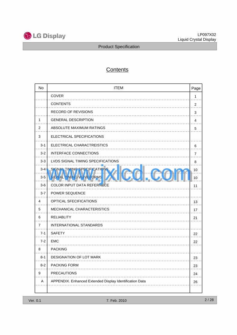
Contents
No ITEM Page
COVER 1
CONTENTS 2
RECORD OF REVISIONS 3
1 GENERAL DESCRIPTION 4
2 ABSOLUTE MAXIMUM RATINGS 5
3 ELECTRICAL SPECIFICATIONS
3-1 ELECTRICAL CHARACTREISTICS 6
3-2 INTERFACE CONNECTIONS 7
3-3 LVDS SIGNAL TIMING SPECIFICATIONS 8
3-4 SIGNAL TIMING SPECIFICATIONS 10
3-5 SIGNAL TIMING WAVEFORMS 10
3-6 COLOR INPUT DATA REFERNECE 11
3-7 POWER SEQUENCE
4 OPTICAL SFECIFICATIONS 13
5 MECHANICAL CHARACTERISTICS 17
6 RELIABLITY 21
7 INTERNATIONAL STANDARDS
7-1 SAFETY 22
7-2 EMC 22
8 PACKING
8-1 DESIGNATION OF LOT MARK 23
8-2 PACKING FORM 23
9 PRECAUTIONS 24
A APPENDIX. Enhanced Extended Display Identification Data 26
www.jxlcd.comwww.jxlcd.com
Product Specification
LP097X02Liquid Crystal Display
Ver. 0.1 7. Feb. 2010 3 / 28
RECORD OF REVISIONS
Revision No Revision Date Page Description EDID ver
0.1 7. Feb. 2010 - First Draft TBD
www.jxlcd.comwww.jxlcd.com
Product Specification
LP097X02Liquid Crystal Display
Ver. 0.1 7. Feb. 2010 4 / 28
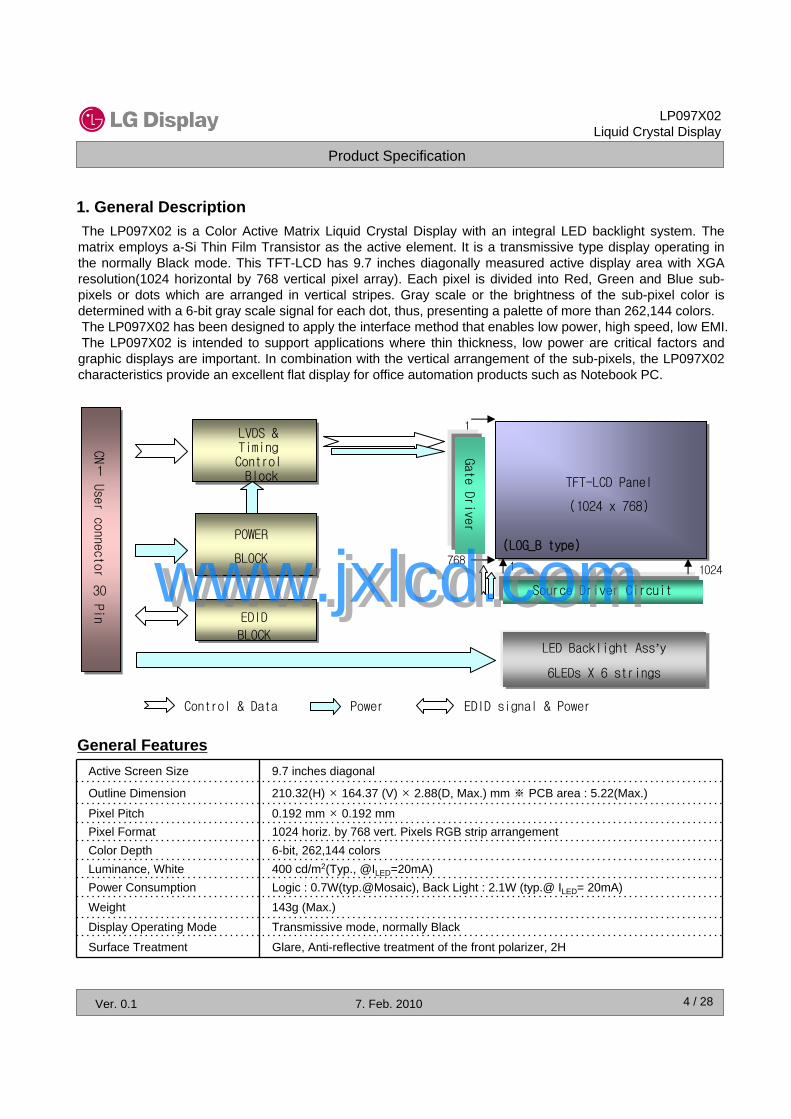
1. General Description
General FeaturesActive Screen Size 9.7 inches diagonal
Outline Dimension 210.32(H) × 164.37 (V) × 2.88(D, Max.) mm ※ PCB area : 5.22(Max.)
Pixel Pitch 0.192 mm × 0.192 mm Pixel Format 1024 horiz. by 768 vert. Pixels RGB strip arrangementColor Depth 6-bit, 262,144 colorsLuminance, White 400 cd/m2(Typ., @ILED=20mA)Power Consumption Logic : 0.7W(typ.@Mosaic), Back Light : 2.1W (typ.@ ILED= 20mA)Weight 143g (Max.)Display Operating Mode Transmissive mode, normally Black
Surface Treatment Glare, Anti-reflective treatment of the front polarizer, 2H
The LP097X02 is a Color Active Matrix Liquid Crystal Display with an integral LED backlight system. The matrix employs a-Si Thin Film Transistor as the active element. It is a transmissive type display operating in the normally Black mode. This TFT-LCD has 9.7 inches diagonally measured active display area with XGA resolution(1024 horizontal by 768 vertical pixel array). Each pixel is divided into Red, Green and Blue sub-pixels or dots which are arranged in vertical stripes. Gray scale or the brightness of the sub-pixel color is determined with a 6-bit gray scale signal for each dot, thus, presenting a palette of more than 262,144 colors.The LP097X02 has been designed to apply the interface method that enables low power, high speed, low EMI. The LP097X02 is intended to support applications where thin thickness, low power are critical factors and graphic displays are important. In combination with the vertical arrangement of the sub-pixels, the LP097X02 characteristics provide an excellent flat display for office automation products such as Notebook PC.
Control & Data Power EDID signal & Power
TFT-LCD Panel
(1024 x 768)
1
7681 1024
CN
1
User connector
30
Pin
POWER
BLOCK
EDID
BLOCK
Gate Driver
Source Driver Circuit
LED Backlight Ass’y
6LEDs X 6 strings
LVDS &TimingControlBlock
(LOG_B type)
www.jxlcd.comwww.jxlcd.com
Product Specification
LP097X02Liquid Crystal Display
Ver. 0.1 7. Feb. 2010 5 / 28
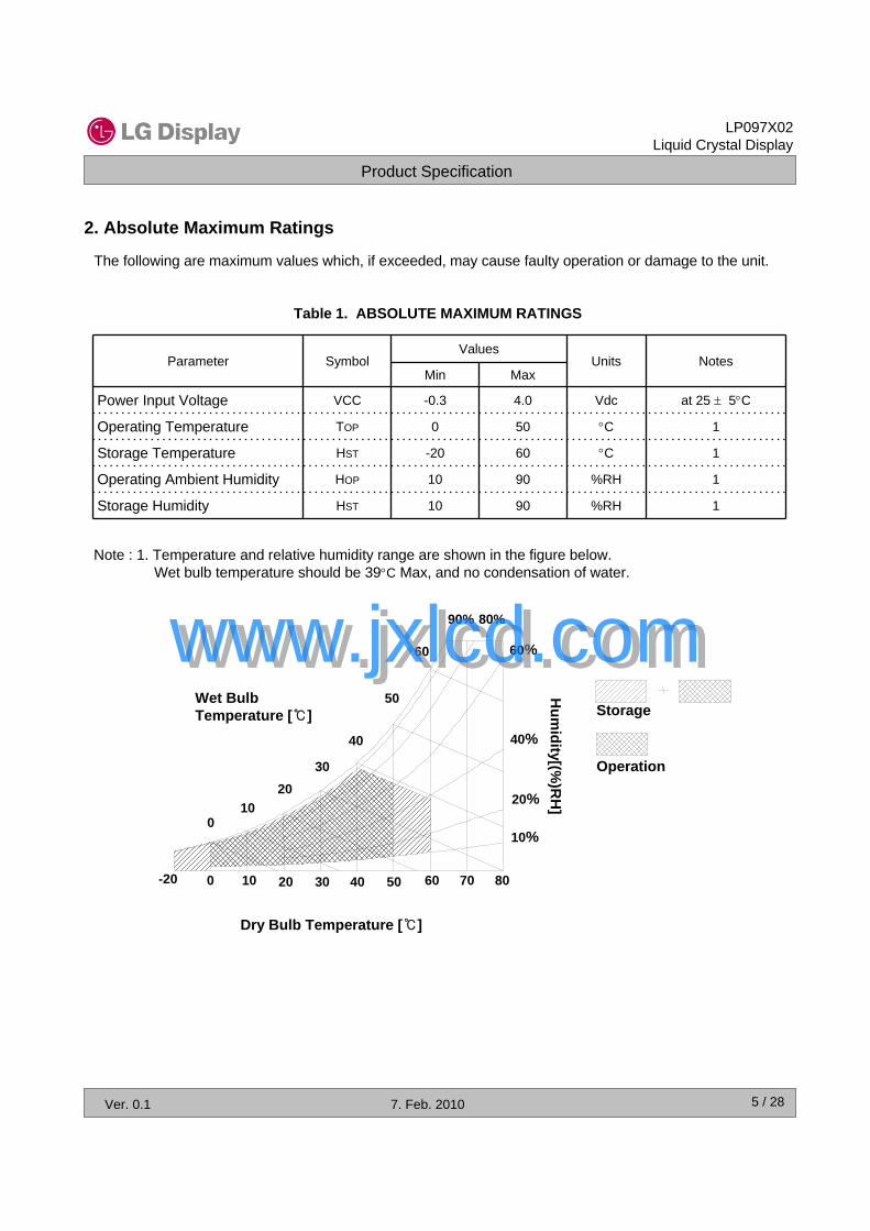
2. Absolute Maximum Ratings
The following are maximum values which, if exceeded, may cause faulty operation or damage to the unit.
Table 1. ABSOLUTE MAXIMUM RATINGS
Storage
Operation
10 20 30 40 50 60 70 800-20
Dry Bulb Temperature [℃]
10%
20%
40%
60%
90% 80%
010
2030
40
50
60
Wet BulbTemperature [℃]
Hum
idity[(%)R
H]
Parameter SymbolValues
Units NotesMin Max
Power Input Voltage VCC -0.3 4.0 Vdc at 25 ± 5°C
Operating Temperature TOP 0 50 °C 1
Storage Temperature HST -20 60 °C 1
Operating Ambient Humidity HOP 10 90 %RH 1
Storage Humidity HST 10 90 %RH 1
Note : 1. Temperature and relative humidity range are shown in the figure below. Wet bulb temperature should be 39°C Max, and no condensation of water.
www.jxlcd.comwww.jxlcd.com
Product Specification
LP097X02Liquid Crystal Display
Ver. 0.1 7. Feb. 2010 6 / 28
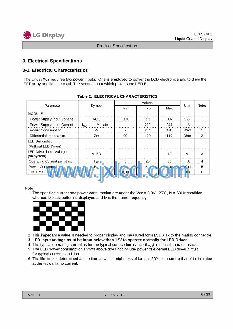
3. Electrical Specifications
3-1. Electrical Characteristics
Table 2. ELECTRICAL CHARACTERISTICS
Parameter SymbolValues
Unit NotesMin Typ Max
MODULE :Power Supply Input Voltage VCC 3.0 3.3 3.6 VDC
Power Supply Input Current ICC Mosaic - 212 244 mA 1Power Consumption Pc - 0.7 0.81 Watt 1Differential Impedance Zm 90 100 110 Ohm 2
LED Backlight : (Without LED Driver)
LED Driver input Volatge(on system) VLED 12 V 3
Operating Current per string ILED 5 20 25 mA 4Power Consumption PBL 2.1 2.6 Watt 5Life Time 10,000 - - Hrs 6
Note)1. The specified current and power consumption are under the Vcc = 3.3V , 25℃, fv = 60Hz condition
whereas Mosaic pattern is displayed and fv is the frame frequency.
2. This impedance value is needed to proper display and measured form LVDS Tx to the mating connector.3. LED input voltage must be input below than 12V to operate normally for LED Driver.4. The typical operating current is for the typical surface luminance (LWH) in optical characteristics.5. The LED power consumption shown above does not include power of external LED driver circuit
for typical current condition. 6. The life time is determined as the time at which brightness of lamp is 50% compare to that of initial value
at the typical lamp current.
The LP097X02 requires two power inputs. One is employed to power the LCD electronics and to drive the TFT array and liquid crystal. The second input which powers the LED BL.
www.jxlcd.comwww.jxlcd.com
Product Specification
LP097X02Liquid Crystal Display
Ver. 0.1 7. Feb. 2010 7 / 28
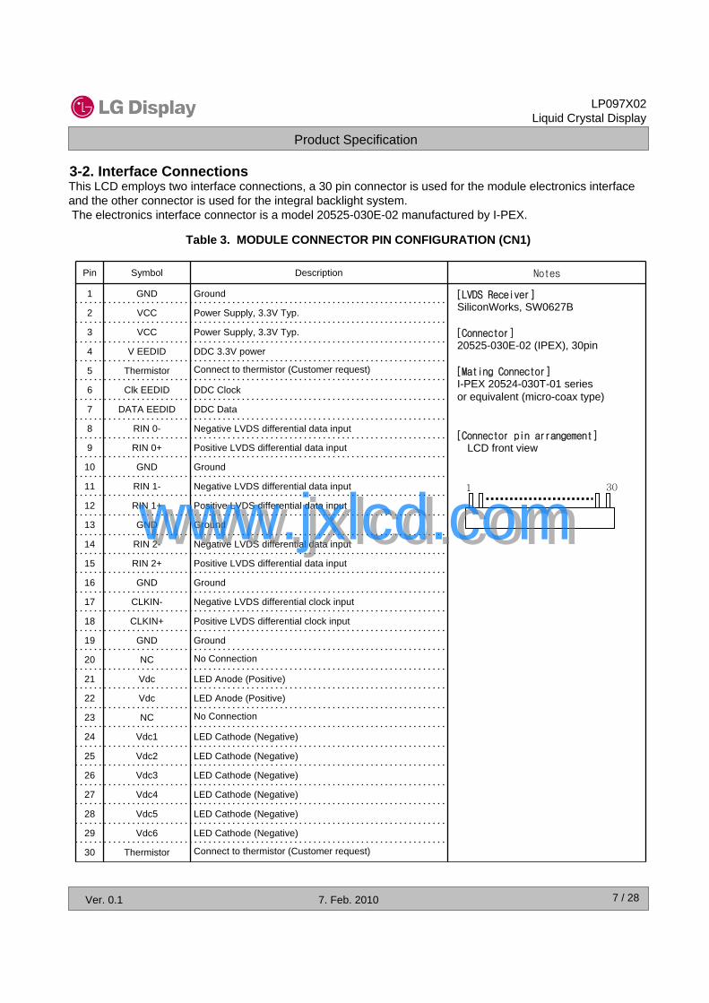
3-2. Interface ConnectionsThis LCD employs two interface connections, a 30 pin connector is used for the module electronics interface and the other connector is used for the integral backlight system.The electronics interface connector is a model 20525-030E-02 manufactured by I-PEX.
Table 3. MODULE CONNECTOR PIN CONFIGURATION (CN1)
Pin Symbol Description Notes
1 GND Ground [LVDS Receiver]SiliconWorks, SW0627B
[Connector]20525-030E-02 (IPEX), 30pin
[Mating Connector]I-PEX 20524-030T-01 seriesor equivalent (micro-coax type)
[Connector pin arrangement]LCD front view
2 VCC Power Supply, 3.3V Typ.
3 VCC Power Supply, 3.3V Typ.
4 V EEDID DDC 3.3V power
5 Thermistor Connect to thermistor (Customer request)
6 Clk EEDID DDC Clock
7 DATA EEDID DDC Data
8 RIN 0- Negative LVDS differential data input
9 RIN 0+ Positive LVDS differential data input
10 GND Ground
11 RIN 1- Negative LVDS differential data input
12 RIN 1+ Positive LVDS differential data input
13 GND Ground
14 RIN 2- Negative LVDS differential data input
15 RIN 2+ Positive LVDS differential data input
16 GND Ground
17 CLKIN- Negative LVDS differential clock input
18 CLKIN+ Positive LVDS differential clock input
19 GND Ground
20 NC No Connection
21 Vdc LED Anode (Positive)
22 Vdc LED Anode (Positive)
23 NC No Connection
24 Vdc1 LED Cathode (Negative)
25 Vdc2 LED Cathode (Negative)
26 Vdc3 LED Cathode (Negative)
27 Vdc4 LED Cathode (Negative)
28 Vdc5 LED Cathode (Negative)
29 Vdc6 LED Cathode (Negative)
30 Thermistor Connect to thermistor (Customer request)
301
www.jxlcd.comwww.jxlcd.com
Product Specification
LP097X02Liquid Crystal Display
Ver. 0.1 7. Feb. 2010 8 / 28
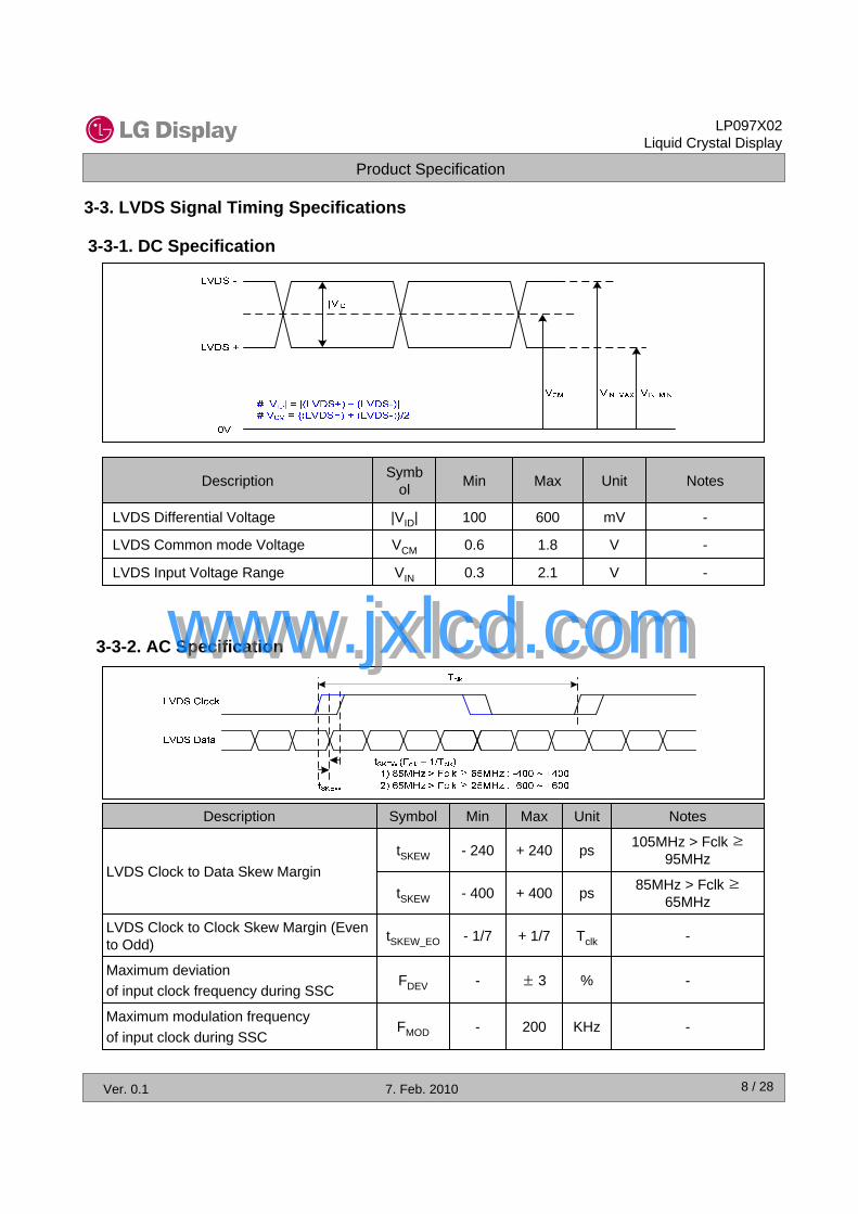
Description Symbol Min Max Unit Notes
LVDS Clock to Data Skew MargintSKEW - 240 + 240 ps 105MHz > Fclk ≥
95MHz
tSKEW - 400 + 400 ps 85MHz > Fclk ≥65MHz
LVDS Clock to Clock Skew Margin (Even to Odd) tSKEW_EO - 1/7 + 1/7 Tclk -
Maximum deviation of input clock frequency during SSC
FDEV - ± 3 % -
Maximum modulation frequency of input clock during SSC
FMOD - 200 KHz -
Description Symbol Min Max Unit Notes
LVDS Differential Voltage |VID| 100 600 mV -
LVDS Common mode Voltage VCM 0.6 1.8 V -
LVDS Input Voltage Range VIN 0.3 2.1 V -
3-3-1. DC Specification
3-3-2. AC Specification
3-3. LVDS Signal Timing Specifications
www.jxlcd.comwww.jxlcd.com
Product Specification
LP097X02Liquid Crystal Display
Ver. 0.1 7. Feb. 2010 9 / 28
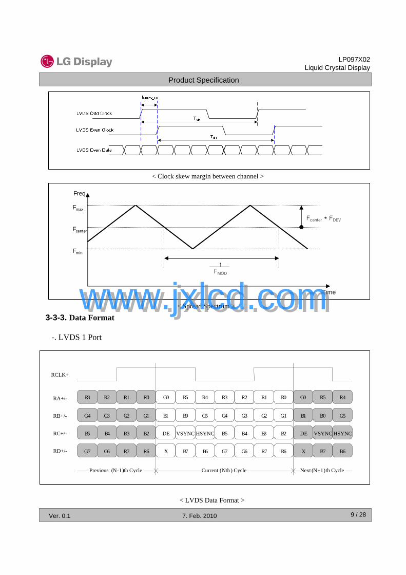
< Clock skew margin between channel >
< LVDS Data Format >
3-3-3. Data Format
-. LVDS 1 Port
< Spread Spectrum >
Time
Fcenter
Fmax
Fmin
FMOD
1
Fcenter * FDEV
Freq.
G0 R5 R4 R3 R2 R1 R0
B1 B0 G5 G4 G3 G2 G1
DE VSYNC HSYNC B5 B4 B3 B2
X B7 B6 G7 G6 R7 R6
R1 R0
G2 G1
B3 B2
R7 R6
G0
B1
DE
X
Current (Nth ) Cycle
R5 R4
B0 G5
VSYNC HSYNC
B7 B6
R3 R2
G4 G3
B5 B4
G7 G6
Previous (N-1)th Cycle Next (N+1)th Cycle
RCLK+
RA+/-
RB+/-
RC+/-
RD+/-
www.jxlcd.comwww.jxlcd.com
Product Specification
LP097X02Liquid Crystal Display
Ver. 0.1 7. Feb. 2010 10 / 28
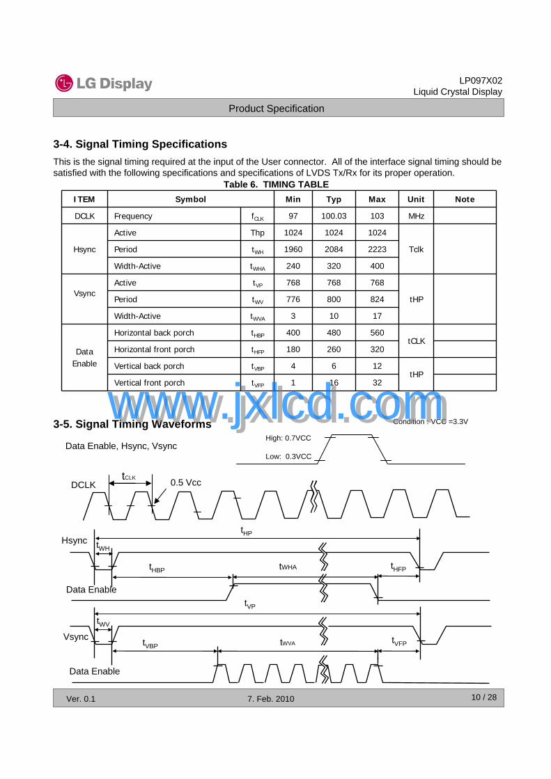
3-4. Signal Timing Specifications
Table 6. TIMING TABLE
This is the signal timing required at the input of the User connector. All of the interface signal timing should be satisfied with the following specifications and specifications of LVDS Tx/Rx for its proper operation.
3-5. Signal Timing Waveforms Condition : VCC =3.3V
Low: 0.3VCC
High: 0.7VCCData Enable, Hsync, Vsync
Hsync
Data Enable
Vsync
Data Enable
tWH
tHP
tHFPtHBP
tVP
tWV
tVBPtVFP
tWHA
tWVA
tCLK 0.5 VccDCLK
ITEM Symbol Min Typ Max Unit Note
DCLK Frequency fCLK 97 100.03 103 MHz
Hsync
Active Thp 1024 1024 1024
TclkPeriod tWH 1960 2084 2223
Width-Active tWHA 240 320 400
VsyncActive tVP 768 768 768
tHPPeriod tWV 776 800 824
Width-Active tWVA 3 10 17
DataEnable
Horizontal back porch tHBP 400 480 560tCLK
Horizontal front porch tHFP 180 260 320
Vertical back porch tVBP 4 6 12tHP
Vertical front porch tVFP 1 16 32
www.jxlcd.comwww.jxlcd.com
Product Specification
LP097X02Liquid Crystal Display
Ver. 0.1 7. Feb. 2010 11 / 28
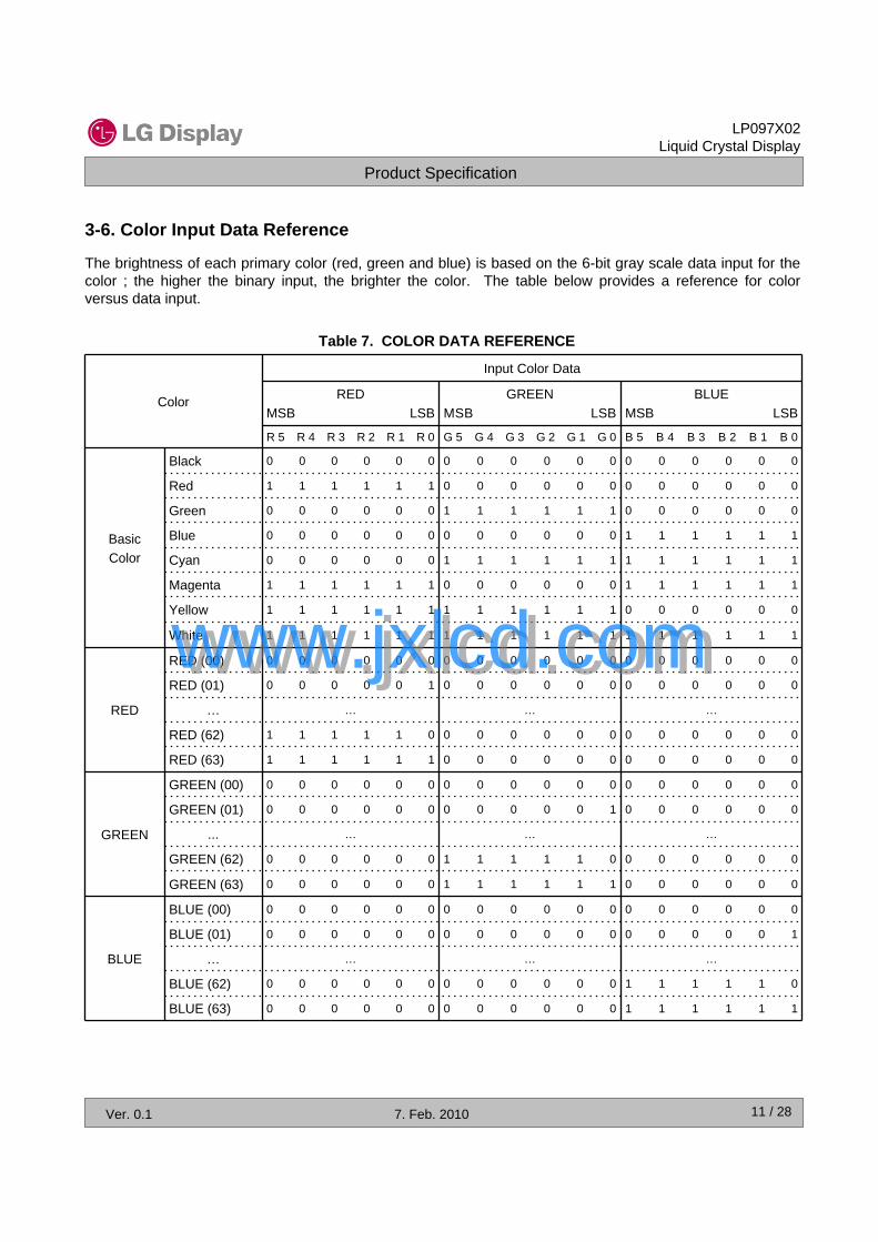
3-6. Color Input Data Reference
The brightness of each primary color (red, green and blue) is based on the 6-bit gray scale data input for thecolor ; the higher the binary input, the brighter the color. The table below provides a reference for color versus data input.
Table 7. COLOR DATA REFERENCE
Color
Input Color Data
REDMSB LSB
GREENMSB LSB
BLUEMSB LSB
R 5 R 4 R 3 R 2 R 1 R 0 G 5 G 4 G 3 G 2 G 1 G 0 B 5 B 4 B 3 B 2 B 1 B 0
BasicColor
Black 0 0 0 0 0 0 0 0 0 0 0 0 0 0 0 0 0 0
Red 1 1 1 1 1 1 0 0 0 0 0 0 0 0 0 0 0 0
Green 0 0 0 0 0 0 1 1 1 1 1 1 0 0 0 0 0 0
Blue 0 0 0 0 0 0 0 0 0 0 0 0 1 1 1 1 1 1
Cyan 0 0 0 0 0 0 1 1 1 1 1 1 1 1 1 1 1 1
Magenta 1 1 1 1 1 1 0 0 0 0 0 0 1 1 1 1 1 1
Yellow 1 1 1 1 1 1 1 1 1 1 1 1 0 0 0 0 0 0
White 1 1 1 1 1 1 1 1 1 1 1 1 1 1 1 1 1 1
RED
RED (00) 0 0 0 0 0 0 0 0 0 0 0 0 0 0 0 0 0 0
RED (01) 0 0 0 0 0 1 0 0 0 0 0 0 0 0 0 0 0 0
… … … …
RED (62) 1 1 1 1 1 0 0 0 0 0 0 0 0 0 0 0 0 0
RED (63) 1 1 1 1 1 1 0 0 0 0 0 0 0 0 0 0 0 0
GREEN
GREEN (00) 0 0 0 0 0 0 0 0 0 0 0 0 0 0 0 0 0 0
GREEN (01) 0 0 0 0 0 0 0 0 0 0 0 1 0 0 0 0 0 0
... … … …
GREEN (62) 0 0 0 0 0 0 1 1 1 1 1 0 0 0 0 0 0 0
GREEN (63) 0 0 0 0 0 0 1 1 1 1 1 1 0 0 0 0 0 0
BLUE
BLUE (00) 0 0 0 0 0 0 0 0 0 0 0 0 0 0 0 0 0 0
BLUE (01) 0 0 0 0 0 0 0 0 0 0 0 0 0 0 0 0 0 1
… … … …
BLUE (62) 0 0 0 0 0 0 0 0 0 0 0 0 1 1 1 1 1 0
BLUE (63) 0 0 0 0 0 0 0 0 0 0 0 0 1 1 1 1 1 1
www.jxlcd.comwww.jxlcd.com
Product Specification
LP097X02Liquid Crystal Display
Ver. 0.1 7. Feb. 2010 12 / 28
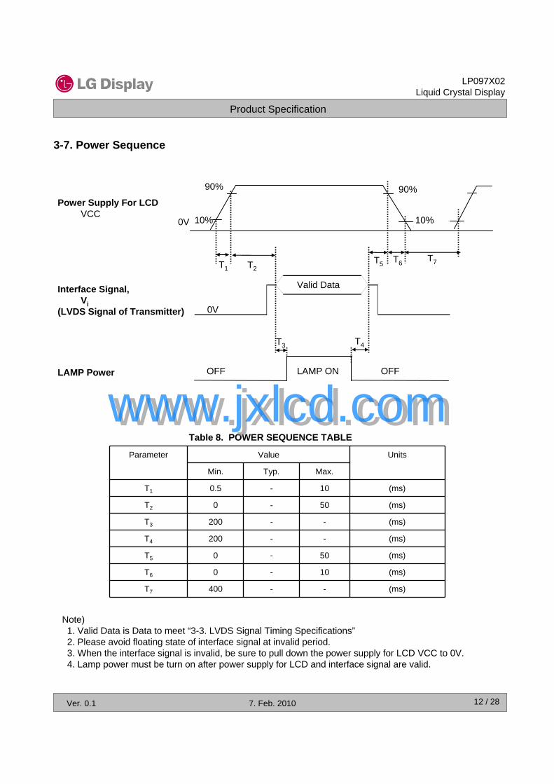
3-7. Power Sequence
Note)1. Valid Data is Data to meet “3-3. LVDS Signal Timing Specifications”2. Please avoid floating state of interface signal at invalid period.3. When the interface signal is invalid, be sure to pull down the power supply for LCD VCC to 0V.4. Lamp power must be turn on after power supply for LCD and interface signal are valid.
Parameter Value Units
Min. Typ. Max.
T1 0.5 - 10 (ms)
T2 0 - 50 (ms)
T3 200 - - (ms)
T4 200 - - (ms)
T5 0 - 50 (ms)
T6 0 - 10 (ms)
T7 400 - - (ms)
Table 8. POWER SEQUENCE TABLE
T6
Interface Signal, Vi
(LVDS Signal of Transmitter)
LAMP Power
Power Supply For LCDVCC
90%
10%10%0V
90%
T1 T2T5
Valid Data
0V
OFFOFF LAMP ON
T7
T3 T4
www.jxlcd.comwww.jxlcd.com
Product Specification
LP097X02Liquid Crystal Display
Ver. 0.1 7. Feb. 2010 13 / 28
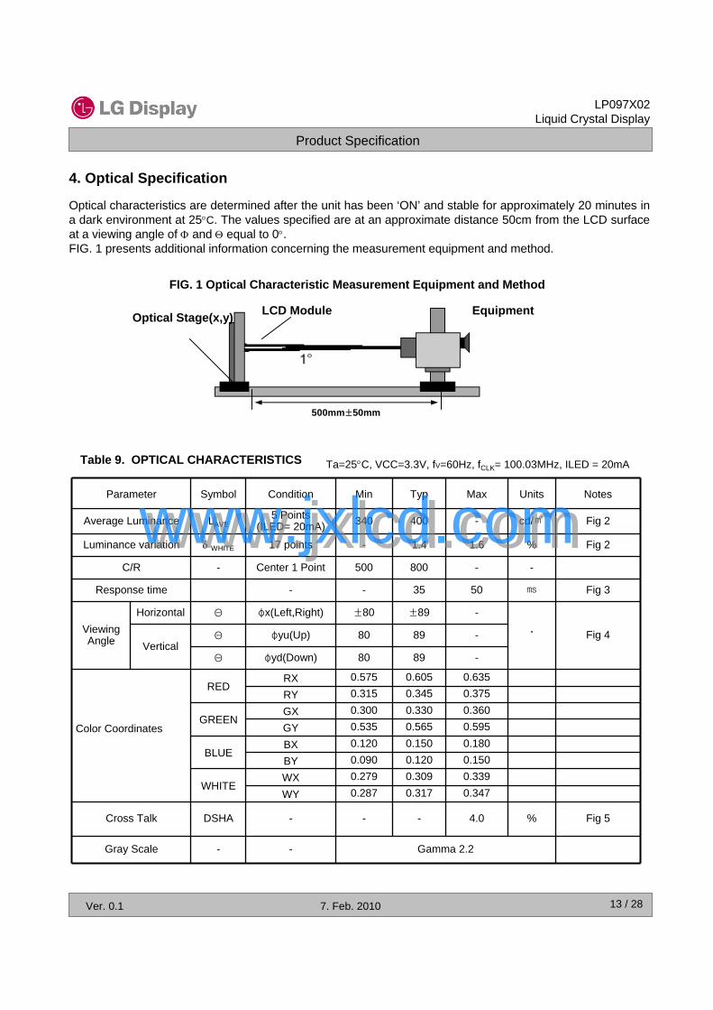
4. Optical Specification
FIG. 1 Optical Characteristic Measurement Equipment and Method
Table 9. OPTICAL CHARACTERISTICS
Optical characteristics are determined after the unit has been ‘ON’ and stable for approximately 20 minutes in a dark environment at 25°C. The values specified are at an approximate distance 50cm from the LCD surface at a viewing angle of Φ and Θ equal to 0°.FIG. 1 presents additional information concerning the measurement equipment and method.
Ta=25°C, VCC=3.3V, fV=60Hz, fCLK= 100.03MHz, ILED = 20mA
LCD ModuleOptical Stage(x,y) Equipment
500mm±50mm
Parameter Symbol Condition Min Typ Max Units Notes
Average Luminance LAVE5 Points
(ILED= 20mA) 340 400 - cd/㎡ Fig 2
Luminance variation δ WHITE 17 points - 1.4 1.6 % Fig 2
C/R - Center 1 Point 500 800 - -
Response time - - 35 50 ㎳ Fig 3
ViewingAngle
Horizontal Θ φx(Left,Right) ±80 ±89 -
˚ Fig 4Vertical
Θ φyu(Up) 80 89 -
Θ φyd(Down) 80 89 -
Color Coordinates
REDRX 0.575 0.605 0.635RY 0.315 0.345 0.375
GREENGX 0.300 0.330 0.360GY 0.535 0.565 0.595
BLUEBX 0.120 0.150 0.180BY 0.090 0.120 0.150
WHITEWX 0.279 0.309 0.339WY 0.287 0.317 0.347
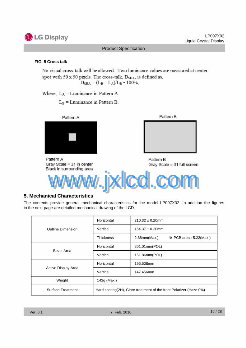
Cross Talk DSHA - - - 4.0 % Fig 5
Gray Scale - - Gamma 2.2
www.jxlcd.comwww.jxlcd.com
Product Specification
LP097X02Liquid Crystal Display
Ver. 0.1 7. Feb. 2010 14 / 28
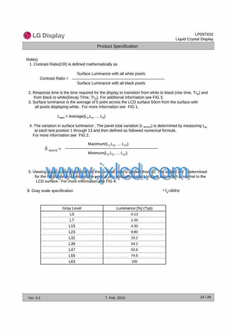
Gray Level Luminance [%] (Typ)L0 0.13
L7 1.00
L15 4.30
L23 9.80
L31 19.2
L39 34.2
L47 53.5
L55 74.5
L63 100
Notes)1. Contrast Ratio(CR) is defined mathematically as
Surface Luminance with all white pixelsContrast Ratio =
Surface Luminance with all black pixels
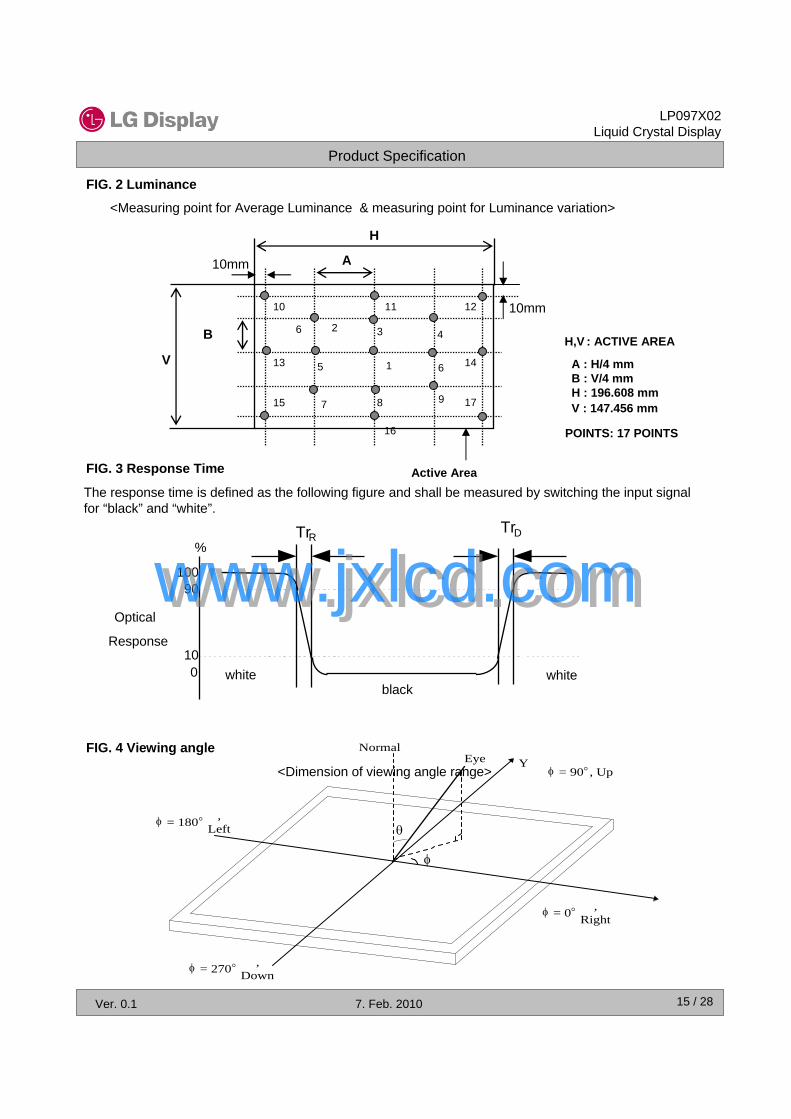
2. Response time is the time required for the display to transition from white to black (rise time, TrR) andfrom black to white(Decay Time, TrD). For additional information see FIG 3.
3. Surface luminance is the average of 5 point across the LCD surface 50cm from the surface withall pixels displaying white. For more information see FIG 1.
LWH = Average(L1,L2, … L5)
4. The variation in surface luminance , The panel total variation (δ WHITE) is determined by measuring LNat each test position 1 through 13 and then defined as followed numerical formula.
For more information see FIG 2.
Maximum(L1,L2, … L17) δ WHITE =
Minimum(L1,L2, … L17)
5. Viewing angle is the angle at which the contrast ratio is greater than 10. The angles are determined for the horizontal or x axis and the vertical or y axis with respect to the z axis which is normal to theLCD surface. For more information see FIG 4.
6. Gray scale specification * fV=60Hz
www.jxlcd.comwww.jxlcd.com
Product Specification
LP097X02Liquid Crystal Display
Ver. 0.1 7. Feb. 2010 15 / 28
FIG. 4 Viewing angle
<Dimension of viewing angle range>
Normal YEye
φ
θ
φ = 0° ,Right
φ = 180° ,Left
φ = 270° ,Down
φ = 90°, Up
FIG. 3 Response Time
The response time is defined as the following figure and shall be measured by switching the input signal for “black” and “white”.
TrR TrD
10090
100
%
Optical
Response
whiteblack
white
FIG. 2 Luminance
<Measuring point for Average Luminance & measuring point for Luminance variation>
: ACTIVE AREA
A : H/4 mmB : V/4 mmH : 196.608 mmV : 147.456 mm
POINTS: 17 POINTS
H,V
Active Area
1
32
5
4
H
A
B
V
10 11 12
13 14
15 8 17
10mm
10mm6
16
7 9
6
www.jxlcd.comwww.jxlcd.com
Product Specification
LP097X02Liquid Crystal Display
Ver. 0.1 7. Feb. 2010 16 / 28
5. Mechanical CharacteristicsThe contents provide general mechanical characteristics for the model LP097X02. In addition the figuresin the next page are detailed mechanical drawing of the LCD.
Outline Dimension
Horizontal 210.32 ± 0.20mm
Vertical 164.37 ± 0.20mm
Thickness 2.88mm(Max.) ※ PCB area : 5.22(Max.)
Bezel AreaHorizontal 201.01mm(POL)
Vertical 151.86mm(POL)
Active Display AreaHorizontal 196.608mm
Vertical 147.456mm
Weight 143g (Max.)
Surface Treatment Hard coating(2H), Glare treatment of the front Polarizer (Haze 0%)
FIG. 5 Cross talk
www.jxlcd.comwww.jxlcd.com

Product Specification
LP097X02Liquid Crystal Display
Ver. 0.1 7. Feb. 2010 17 / 28
<FRONT VIEW>
www.jxlcd.comwww.jxlcd.com
Product Specification
LP097X02Liquid Crystal Display
Ver. 0.1 7. Feb. 2010 18 / 28
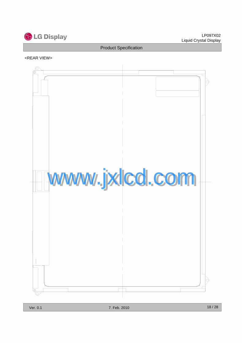
<REAR VIEW>
www.jxlcd.comwww.jxlcd.com
Product Specification
LP097X02Liquid Crystal Display
Ver. 0.1 7. Feb. 2010 19 / 28
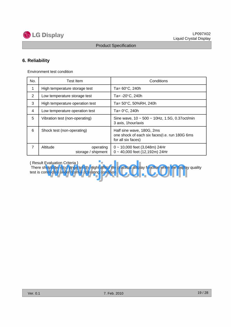
6. Reliability
Environment test condition
{ Result Evaluation Criteria }There should be no change which might affect the practical display function when the display qualitytest is conducted under normal operating condition.
No. Test Item Conditions
1 High temperature storage test Ta= 60°C, 240h
2 Low temperature storage test Ta= -20°C, 240h
3 High temperature operation test Ta= 50°C, 50%RH, 240h
4 Low temperature operation test Ta= 0°C, 240h
5 Vibration test (non-operating) Sine wave, 10 ~ 500 ~ 10Hz, 1.5G, 0.37oct/min3 axis, 1hour/axis
6 Shock test (non-operating) Half sine wave, 180G, 2msone shock of each six faces(I.e. run 180G 6msfor all six faces)
7 Altitude operatingstorage / shipment
0 ~ 10,000 feet (3,048m) 24Hr0 ~ 40,000 feet (12,192m) 24Hr
www.jxlcd.comwww.jxlcd.com

Product Specification
LP097X02Liquid Crystal Display
Ver. 0.1 7. Feb. 2010 20 / 28
7. International Standards
7-1. Safety
7-2. EMC
a) ANSI C63.4 “Methods of Measurement of Radio-Noise Emissions from Low-Voltage Electrical and Electrical Equipment in the Range of 9kHZ to 40GHz. “American National Standards Institute(ANSI),1992b) C.I.S.P.R “Limits and Methods of Measurement of Radio Interface Characteristics of InformationTechnology Equipment.“ International Special Committee on Radio Interference.c) EN 55022 “Limits and Methods of Measurement of Radio Interface Characteristics of InformationTechnology Equipment.“ European Committee for Electrotechnical Standardization.(CENELEC), 1998( Including A1: 2000 )
a) UL 60950-1:2003, First Edition, Underwriters Laboratories, Inc.,Standard for Safety of Information Technology Equipment.b) CAN/CSA C22.2, No. 60950-1-03 1st Ed. April 1, 2003, Canadian Standards Association,Standard for Safety of Information Technology Equipment.c) EN 60950-1:2001, First Edition, European Committee for Electrotechnical Standardization(CENELEC)European Standard for Safety of Information Technology Equipment.
www.jxlcd.comwww.jxlcd.com

Product Specification
LP097X02Liquid Crystal Display
Ver. 0.1 7. Feb. 2010 21 / 28
8. Packing
8-2. Packing Form
8-1. Designation of Lot Marka) Lot Mark
A B C D E F G H I J K L M
A,B,C : SIZE(INCH) D : YEAR E : MONTH F ~ M : SERIAL NO.
Note1. YEAR
2. MONTH
Mark
Year
0
2010
6
2006
7
2007
8
2008
9
2009
4
2004
5
2005
321
200320022001
B
Nov
Mark
Month
A
Oct
6
Jun
7
Jul
8
Aug
9
Sep
4
Apr
5
May
C321
DecMarFebJan
b) Location of Lot Mark
Serial No. is printed on the label. The label is attached to the backside of the LCD module.This is subject to change without prior notice.
a) Package quantity in one box : 30 pcs
b) Box Size : 478mm × 365mm × 328mm
www.jxlcd.comwww.jxlcd.com
Product Specification
LP097X02Liquid Crystal Display
Ver. 0.1 7. Feb. 2010 22 / 28
9. PRECAUTIONS
Please pay attention to the followings when you use this TFT LCD module.
9-1. MOUNTING PRECAUTIONS(1) You must mount a module using holes arranged in four corners or four sides.(2) You should consider the mounting structure so that uneven force (ex. Twisted stress) is not applied to the
module. And the case on which a module is mounted should have sufficient strength so that external force is not transmitted directly to the module.
(3) Please attach the surface transparent protective plate to the surface in order to protect the polarizer.Transparent protective plate should have sufficient strength in order to the resist external force.
(4) You should adopt radiation structure to satisfy the temperature specification.(5) Acetic acid type and chlorine type materials for the cover case are not desirable because the former
generates corrosive gas of attacking the polarizer at high temperature and the latter causes circuit break by electro-chemical reaction.
(6) Do not touch, push or rub the exposed polarizers with glass, tweezers or anything harder than HBpencil lead. And please do not rub with dust clothes with chemical treatment.Do not touch the surface of polarizer for bare hand or greasy cloth.(Some cosmetics are detrimentalto the polarizer.)
(7) When the surface becomes dusty, please wipe gently with absorbent cotton or other soft materials like chamois soaks with petroleum benzene. Normal-hexane is recommended for cleaning the adhesives used to attach front / rear polarizers. Do not use acetone, toluene and alcohol because they cause chemical damage to the polarizer.
(8) Wipe off saliva or water drops as soon as possible. Their long time contact with polarizer causes deformations and color fading.
(9) Do not open the case because inside circuits do not have sufficient strength.
9-2. OPERATING PRECAUTIONS
(1) The spike noise causes the mis-operation of circuits. It should be lower than following voltage : V=± 200mV(Over and under shoot voltage)
(2) Response time depends on the temperature.(In lower temperature, it becomes longer.)(3) Brightness depends on the temperature. (In lower temperature, it becomes lower.)
And in lower temperature, response time(required time that brightness is stable after turned on) becomeslonger.
(4) Be careful for condensation at sudden temperature change. Condensation makes damage to polarizer or electrical contacted parts. And after fading condensation, smear or spot will occur.
(5) When fixed patterns are displayed for a long time, remnant image is likely to occur.(6) Module has high frequency circuits. Sufficient suppression to the electromagnetic interference shall be
done by system manufacturers. Grounding and shielding methods may be important to minimized theinterference.
www.jxlcd.comwww.jxlcd.com

Product Specification
LP097X02Liquid Crystal Display
Ver. 0.1 7. Feb. 2010 23 / 28
Since a module is composed of electronic circuits, it is not strong to electrostatic discharge. Make certain that treatment persons are connected to ground through wrist band etc. And don’t touch interface pin directly.
9-3. ELECTROSTATIC DISCHARGE CONTROL
Strong light exposure causes degradation of polarizer and color filter.
9-4. PRECAUTIONS FOR STRONG LIGHT EXPOSURE
9-5. STORAGE
(1) When the protection film is peeled off, static electricity is generated between the film and polarizer.This should be peeled off slowly and carefully by people who are electrically grounded and with wellion-blown equipment or in such a condition, etc.
(2) The protection film is attached to the polarizer with a small amount of glue. If some stress is appliedto rub the protection film against the polarizer during the time you peel off the film, the glue is apt toremain on the polarizer.Please carefully peel off the protection film without rubbing it against the polarizer.
(3) When the module with protection film attached is stored for a long time, sometimes there remains avery small amount of glue still on the polarizer after the protection film is peeled off.
(4) You can remove the glue easily. When the glue remains on the polarizer surface or its vestige isrecognized, please wipe them off with absorbent cotton waste or other soft material like chamoissoaked with normal-hexane.
9-6. HANDLING PRECAUTIONS FOR PROTECTION FILM
When storing modules as spares for a long time, the following precautions are necessary.
(1) Store them in a dark place. Do not expose the module to sunlight or fluorescent light. Keep the temperature between 5°C and 35°C at normal humidity.
(2) The polarizer surface should not come in contact with any other object.It is recommended that they be stored in the container in which they were shipped.
www.jxlcd.comwww.jxlcd.com

Product Specification
LP097X02Liquid Crystal Display
Ver. 0.1 7. Feb. 2010 24 / 28
APPENDIX A. Enhanced Extended Display Identification Data (EEDIDTM) 1/3
TBDwww.jxlcd.comwww.jxlcd.com

Product Specification
LP097X02Liquid Crystal Display
Ver. 0.1 7. Feb. 2010 25 / 28
APPENDIX A. Enhanced Extended Display Identification Data (EEDIDTM) 2/3
TBDwww.jxlcd.comwww.jxlcd.com
Product Specification
LP097X02Liquid Crystal Display
Ver. 0.1 7. Feb. 2010 26 / 28
APPENDIX A. Enhanced Extended Display Identification Data (EEDIDTM) 3/3
TBDwww.jxlcd.comwww.jxlcd.com