Embed Size (px)
Citation preview

SPECIFICATION
CUSTOMER :
MODULE NO.: WG240128B-FMI-VZ#
APPROVED BY:
( FOR CUSTOMER USE ONLY )
PCB VERSION: DATA:
SALES BY APPROVED BY CHECKED BY PREPARED BY
ISSUED DATE:
1 46 www.sycelectronica.com.ar

MODLE NO
RECORDS OF REVISION DOC. FIRST ISSUE
VERSION DATE
REVISEDPAGE NO. SUMMARY
0 2007/12/21
First issue
2 46 www.sycelectronica.com.ar

Contents
1.Module Classification Information 2.Precautions in use of LCD Modules 3.General Specification 4.Absolute Maximum Ratings 5.Electrical Characteristics 6.Optical Characteristics 7.Power Supply for LCD Module and Contrast Adjust 8.Counter Drawing & Block Diagram 9.Interface Pin Function 10.Display control instruction 11.Timing Characteristics 12.Reliability 13.Backlight Information 14. Inspection specification 15. Material List of Components for RoHs
3 46 www.sycelectronica.com.ar

1.Module Classification Information
W G 2 4 0 1 2 8 BF M I VZ#
BrandWINSTAR DISPLAY CORPORATION
Display TypeHCharacter Type, GGraphic Type
Display Font240 * 128
Model serials no.
Backlight Type NWithout backlight
BEL, Blue green
DEL, Green
WEL, White
FCCFL, White
YLED, Yellow Green
TLED, White
ALED, Amber
RLED, Red
OLED, Orange
GLED, Green
LCD Mode BTN Positive, Gray
NTN Negative,
GSTN Positive, Gray
YSTN Positive, Yellow Green
MSTN Negative, Blue
FFSTN Positive
TFSTN Negative
LCD Polarizer Type/ Temperature range/ View direction
AReflective, N.T, 6:00
DReflective, N.T, 12:00
GReflective, W. T, 6:00
JReflective, W. T, 12:00
BTransflective, N.T,6:00
ETransflective, N.T.12:00
HTransflective, W.T,6:00
KTransflective, W.T,12:00
CTransmissive, N.T,6:00
FTransmissive, N.T,12:00
ITransmissive, W. T, 6:00
LTransmissive, W.T,12:00
Special Code V : Build in Negative voltage ; Z:ICNT7086 #:Fit in with the ROHS Directions and regulations
4 46 www.sycelectronica.com.ar

2.Precautions in use of LCD Modules
(1) Avoid applying excessive shocks to the module or making any alterations or modifications to it.
(2) Don’t make extra holes on the printed circuit board, modify its shape or change the components of
LCD module.
(3) Don’t disassemble the LCM.
(4) Don’t operate it above the absolute maximum rating.
(5) Don’t drop, bend or twist LCM.
(6) Soldering:only to the I/O terminals.
(7) Storage:please storage in anti-static electricity container and clean environment.
(8) Winstar have the right to change the passive components
(9) Winstar have the right to change the PCB Rev.
3.General Specification
ITEM STANDARD VALUE UNIT
Number of Dots: 240 ×128
Module dimension: 152.0×104.0×14.3(MAX)mm mm
View area: 114.0×64.0mm mm
Active area: 107.98×57.58mm mm
Character size: (L)0.43×(W)0.43 mm mm
Character pitch: (L)0.45×(W)0.45mm mm
LCD type: STN Negative, Blue Transmissive
Duty: 1/128
View direction: 6 o’clock
Backlight: CCFL White
5 46 www.sycelectronica.com.ar

4.Absolute Maximum Ratings
ITEM SYMBOL MIN. TYP. MAX. UNIT
Operating Temperature TOP -20 +70
Storage Temperature TST -30 +80
Input Voltage VI VSS VDD V
Supply Voltage For Logic VDD-VSS -0.3 +7 V
Supply Voltage For LCD VDD-V0 0 21 V
5.Electrical Characteristics
ITEM SYMBOL CONDITION MIN. TYP. MAX. UNIT
Supply Voltage For Logic VDD-VSS 4.75 5.0 5.25 V
Supply Voltage For LCD VDD-V0
Ta=-20
Ta=25
Ta=70
17.6
19.5
21.7
V
V
V
Input High Vol VIH VDD-2.2 VDD V
Input Low Vol VIL 0 0.8 V
Output High Vol VOH VDD-0.3 VDD V
Output Low Vol. VOL 0 0.3 V
Supply Current IDD VDD=5V 45 mA
6 46 www.sycelectronica.com.ar

6.Optical Characteristics
ITEM SYMBAL CONDITION MIN. TYP. MAX. UNIT
(V) CR2 20 40 deg View Angle
(H) CR2 -30 30 deg
Contrast Ratio CR 3
T rise 200 300 ms Response Time
T fall 200 300 ms
6.1 Definitions
View Angles Contrast Ratio
Response Time
LCD
Z
Y
X
θ
φ
( Best visual angle direction )
( Visual angle direction )
Brightness at non-selected state ( Bns )Brightness at selected state ( BS )
Non-selected state
Operating voltage for LCD driving
CR =
Selected state
Brig
htne
s s (%
)
Bns
Bs
7 46
100
%
90 %
Rise Time Decay Time ( fall time tf )
Brig
htne
ss
Selected ConditionNonselected Condition Nonselected Condition
tr td
10 %
www.sycelectronica.com.ar

7.Power Supply for LCD Module and Contrast Adjust
VDD-V0:LCD Operating Voltage
VDD
VO
VSS
LCDMODULE
5 V10 KΩ
2
1
3
17VEE ( - 16 V )
8 46 www.sycelectronica.com.ar

8.Counter Drawing & Block Diagram 20
.21
57.5
8(A
A)
104.
00.
5
144.0 0.5
240*128 DOTS
18.0115.0
107.98(AA)114.0(VA)
13.74 P2.54x19=48.263.0
8.0 128.0
17.0
64.0
(VA
)74
.012
.0
138.0
4- 3.5 PTH4- 7.0 PAD
2.0
20- 1.0 PTH20- 2.0 PAD
120
152.0 0.5
97.0
3.5
The non-specified tolerance of dimension is 0.3mm.
0.45
0.43
0.450.43
DOT SIZE
L32Column
Column select
HM D240
FS NT7086
Com
64~128
Com
Driver
NT7086NT7086NT7086
NT7086
Frame(Bezel)
Font select
FS H L8X86X8Font
MD2
Vdd,Vss
Vdd
,Vss
,V1,
V4,
V5
Controller
(32K optional)
8KDataAddress
SRAM
T6963C
EDHSCPFRLPCData
RESETC/D
Seg DriverSeg81~160
Com
1~64
Com
Driver
External contrast adjustment.
10K~20KVR
VeeVoVdd
N.V.GeneratorPower Circuit
Bias and
Vdd,Vss,V2,V3,V5
Seg160~240Seg1~80
Seg DriverSeg Driver
240X128 DOT68 seriesor
DB0~DB7
CERDWR
80 series
MPU
125.0 10
9.214.3 MAX
1.6
CCFL B/L
RESET1617
1920
18Vee
FS1NC
MD2
15 CEDB7
VddVoC/DRD
23
56
4
DB0DB1DB2DB3
98
1011
7WR
1 Vss
DB5DB613
14
12DB4
9 46 www.sycelectronica.com.ar

9 terfa Pin un n.In ce F ctio
Pin No. Symbol Level Description
1 Vss GND
2 Vdd Power supply ( +5 V )
3 Vo Power supply for LCD driver
4 C/D H / L WR=L , C/D=H : Command Write C/D=L: Data write
RD=L , C/D=H : Status Read C/D=L: Data read
5 RD L Data read. Read data from T6963C when RD = L
6 WR L Data write. Write data into T6963C when WR = L
7 DB0 H / L Data bus line
8 DB1 H / L Data bus line
9 DB2 H / L Data bus line
10 DB3 H / L Data bus line
11 DB4 H / L Data bus line
12 DB5 H / L Data bus line
13 DB6 H / L Data bus line
14 DB7 H / L Data bus line
15 CE L L : Chip enable
16 RESET H / L H : Normal ; L : Initialize T6963C
17 Vee Negative Voltage output
18 MD2 H / L H: 32 columns ; L: 40 columns
19 FS1 H / L Pins for selection of font ; H : 6 * 8 , L : 8 * 8
20 NC No connection
10 46 www.sycelectronica.com.ar

10.Display control instruction
The LCD Module has built in a T6963C LSI controller, It has an 8-bit parallel data bus and control
lines for writing or reading through an MPU interface, it has a 128-word character generator ROM ( refer to
Table 1. ), which can control an external display RAM of up to 8K bytes. Allocation of text, graphics and
external character generator RAM can be made easily and the display window can be moved freely within
the allocated memory range.
•RAM Interface
The external RAM is used to store display data( text, graphic and external CG data ). It can be freely
allocated to the memory area( 8 Kbyte max ).
Recommend
TEXT AREA
GRAPHIC AREA
CG RAM AREA
0000H
0C00H
1800H
2000H
11 46 www.sycelectronica.com.ar

munications with MPU
(1
must be performed before data is read or written.
Flowchart of com
)Status Read
A status check
Status check
Th atus of T6963C cae St n be read from the data lines.
RD L
WR H
CE L
C/D H
Do to D7 H
The T6963C status word format is as follows:
M
S S S S S S S S
SB LSB
TA7 TA6 TA5 TA4 TA3 TA2 TA1 TA0
D7 D6 D5 D4 D3 D2 D1 D0
0:Disable STA0 Check command execution capability 1:Enable
STA1 Check data read/write Capability 0:Disable 1:Enable
STA2 Check Auto mode data read capability 0:Disable 1:Enable
STA3 Check Auto mode data write capability 0:Disable1:Enable
STA4 Not used
STA5 Check controller operation capability 0:Disable 1:Enable
STA6 Error flag. Used for Screen Peek and Screen copy commands.
0:No error 1:Error
ST al display A7 Check the blink condition 1:Norm0:Disable off
(Note 1) It is necessary to check STA0 and STA1 at the same time.
There is a possibility of erroneous operation due to a hardware interrupt.
A3 are valid in Auto mode; STA0 and STA1 are invalid.
(Note 2) For most modes STA0/STA1 are used as a status check.
(Note 3) STA2 and ST
12 46 www.sycelectronica.com.ar

Status Checking flow
(a) (b)
(Note 4)
tus check is not carried out, the T6963C cannot operate normally, even after a delay
us.
mmand is sent, there is the
possibility that the command or data date will not be received.
When using the MSB=0 command, a Status Read must be performed.
If a sta
time.
The hardware interrupt occurs during the address calculation period (at the end of each line).
If a MSB=0 command is sent to the T6963C during this period, the T6963C enters Wait stat
If a status check is not carried out in this state before the next co
13 46 www.sycelectronica.com.ar

(2)Setting date
When using the T6963C, first set the data, then set the command.
Procedure for sending a command
(a)The case of 1 date (b)The case of 2 data
(Note) When sending more than two data, the last datum (or last two data)is valid.
14 46 www.sycelectronica.com.ar

COMMAND DEFINITIONS
COMMAND CODE D1 D2 FUNCTION
Set Cursor Pointer Y address X address 00100001 Set Offset Register 00H Date REGISTERS SETTING 00100010 Set Address Pointer High address Low address 00100100
Set Text Home Address Low address
SET CONTROL WORD
01000000 Columns 01000001
Low address Columns
High address 00H
High address 00H
01000010 01000011
Set Text Area Set Graphic Home Address Set Graphic Area
MODE SET
1000×000 1000×001 1000×011 1000×100 10000××× 10001×××
OR mode EXOR mode AND mode Text Attribute mode Internal CG ROM mode External CG RAM mode
DISPLAY MODE
10010000 1001××10 10001××11 100101×× 100110×× 100111××
Display off Cursor on, blink off Cursor on, blink on Text on, graphic off Text off, graphic on Text on, graphic on
CURSOR PATTERN SELECT
10100000 10100001 10100010 10100011 10100100 10100101 10100110 10100111
1-line cursor 2-line cursor 3-line cursor 4-line cursor 5-line cursor 6-line cursor 7-line cursor 8-line cursor
DATA AUTO READ/WRITE
10110000 10110001 10110010
Set Data Auto Write Set Data Auto Read Auto Reset
DATA READ/WRITE
11000000 11000001 11000010 11000011 11000100 11000101
Data
Data
Data
Data Write and Increment ADP Data Read and Increment ADP Data Write and Decrement ADP Data Read and Decrement ADP Data Write and Nonvariable ADP Data Read and Nonvariable ADP
SCREEN PEEK 11100000 Screen Peek
X : invalid COMMAND CODE D1 D2 FUNCTION
15 46 www.sycelectronica.com.ar

SCREEN COPY 11101000 Screen Copy
BIT SET/RESET
11110××× 11111××× 1111×000 11111×001 11111×010 11111×011 11111×100 11111×101 11111×110 11111×111
Bit Reset Bit Set Bit 0 (LSB) Bit 1 Bit 2 Bit 3 Bit 4 Bit 5 Bit 6 Bit 7 (MSB)
X : invalid
Setting registers
CODE HEX. FUNCTION D1 D2 00100001 21H SET CURSOR POINTER X ADRS Y ADRS 00100010 22H SET OFFSET REGISTER DATA 00H 00100100 24H SET ADDRESS POINTER LOW ADRS HIGH ADRS
(1)Set Cursor Pointer
The position of the cursor is specified by X ADRS and Y ADRS. The cursor position can only be moved
by this command. Data read/write from the MPU never changes the cursor pointer. X ADRS and Y
ADRS are specified as follows.
X ADRS 00H to 4FH (lower 7 bits are valid)
Y ADRS 00H to 0FH
Y ADRS 00H to 1FH (lower 5 bits are valid)
Single-Scan
X ADRS 00 to 4FH
(2)Set Offset Register
The offset register is used to determine the external character generator RAM area.
The T6963C has a 16-bit address bus as follows.
16 46 www.sycelectronica.com.ar

T6963C assign External character generator, when character code set 80H TO FFH in using internal
character generator. Character code 00H to 80H assign External character generator, when External
generator mode.
The senior five bits define the start address in external memory of the CG RAM area. The next eight
bits represent the character code of the character. In internal CG ROM, character codes 00H to 7FH
represent the predefined “internal” CG ROM characters, and codes 80H to FFH represent the user’s
own “external” characters. In external CG ROM mode, all 256 codes from 00H to FFH can be used to
represent the user’s own characters. The three least significant bits indicate one of the eight rows of
eight dots that define the character’s shape.
The relationship between display RAM address and offset register
Offset register data CG RAM hex. address (start to end)
00000 0000 to 07 FFH
00001 0800 to 0FFFH
00010 1000 to 17FFH
11100 E000 to E7FFH
11101 E800 to EFFFH
11110 F000 to F7FFH
11111 F800 to FFFFH
(Example 1)
Offset register 02H
Character code 80H
Character generator RAM start address 0001 0100 0000 0000
1 4 0 0 H
17 46 www.sycelectronica.com.ar
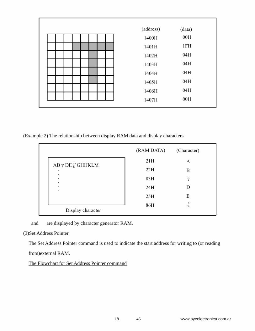
(Example 2) The relationship between display RAM data and display characters
and are displayed by character generator RAM.
(3)Set Address Pointer
The Set Address Pointer command is used to indicate the start address for writing to (or reading
from)external RAM.
The Flowchart for Set Address Pointer command
18 46 www.sycelectronica.com.ar

19 46 www.sycelectronica.com.ar

Set Control Word
CODE HEX. FUNCTION D1 D2
01000000 40H Set Text Home Address Low address High address
01000001 41H Set Text Area Columns 00H
01000010 42H Set Graphic Home Address Low address High address
01000011 43H Set Graphic Area Columns 00H
The home address and column size are defined by this command.
(1)Set Text Home Address
The starting address in the external display RAM for text display is defined by this command.
The text home address indicates the leftmost and uppermost position.
The relationship between external display RAM address and display position
TH TH+CL
TH+TA TH+TA+CL
(TH+TA)+TA TH+2TA+CL
(TH+2TA)+TA TH+3TA+CL
TH+(n-1)TA TH+(n-1)TA+CL
TH:Text home address TA:Text area number (columns) CL:Columns are fixed by hardware (pin-programmable).
(Example) Text home address 0000H Text area 0020H 32 Columns 4 Lines
0000H 0001H 001EH 001FH
0020H 0021H 003EH 002FH
0040H 0041H 005EH 005FH
0060H 0061H 007EH 007FH
20 46 www.sycelectronica.com.ar

(2)Set Graphic Home Address
The starting address of the external display RAM used for graphic display is defined by this command.
The graphic home address indicates the leftmost and uppermost position.
The relationship between external display RAM address and display position
GH GH+GL
GH+GA GH+GA+CL
(GH+GA)+GA GH+2GA+CL
(GH+2GA)+GA GH+3GA+CL
GH+(n-1)GA GH+(n-1)GA+CL
GH:Graphic home address
GA:Graphic area number (columns)
CL:Columns are fixed by hardware (pin-programmable).
(Example)
Graphic home address 0000H
Graphic area 0020H
32 Columns
2 Lines
21 46 www.sycelectronica.com.ar

0000H 0001H 001EH 001FH
0020H 0021H 003EH 003FH
0040H 0041H 005EH 005FH
0060H 0061H 007EH 007FH
0080H 0081H 009EH 009FH
00A0H 00A1H 00BEH 00BFH
00C0H 00C1H 00DEH 00DFH
00E0H 00E1H 00FEH 00FFH
0100H 0101H 011EH 011FH
0120H 0121H 013EH 013FH
0140H 0141H 015EH 014FH
0160H 0161H 017EH 017FH
0180H 0181H 109EH 019FH
01A0H 01A1H 01BEH 01BFH
01C0H 01C1H 01DEH 01DFH
01E0H 01E1H 01FEH 01FFH
(3)Set Text Area
The display columns are defined by the hardware Setting. This command can be used to adjust the
columns of the display.
(Example)
LCD size 20 columns, 4lines
Text home address 0000H
Text area 0014H
Set 32 columns, 4 Lines
0000 0001 ……… 0013 0014 ……… 001F
0014 0015 0027 0028 ……… 0033 ………
0028 0029 ……… 003B 003C ……… 0047
003C 003D ……… 004F 0050 ……… 005B
LCD
22 46 www.sycelectronica.com.ar

(4)Set Graphic Area
The display columns are defined by the hardware setting. This command can be used to adjust the
columns of the graphic display.
(Example)
LCD size 20 columns, 2lines
Graphic home address 0000H
Graphic are 0014H
Set 32 columns, 2 Lines
0000 0001 ……… 0013 0014 ……… 001F
0014 0015 ……… 0027 0028 ……… 0033
0028 0029 003B 003C ……… 0047 ………
003C 003D ……… 004F 0050 ……… 005B
0050 0051 ……… 0063 0064 ……… 006F
0064 0065 0077 0078 ……… 0083 ………
0078 0079 ……… 008B 008C ……… 0097
008C 008D 009F 00A0 00AB ……… ………
00A0 00A1 ……… 00B3 00B4 ……… 00BF
00B4 00B5 ……… 00C7 00C8 ……… 00D3
00C8 00C9 ……… 00DB 00DC ……… 00E7
00DC 00DD ……… 00EF 00F0 ……… 00FD
00F0 00F1 0103 0104 011F ……… ………
0104 0105 ……… 0127 0128 ……… 0123
0128 0129 ……… 013B 0013C ……… 00147
013C 013D ……… 014F 0150 ……… 015B
LCD
If the graphic area setting is set to match the desired number of columns on the LCD, the addressing
scheme will be automatically modified so that the start address of each line equals the end address of
the previous line +1.
23 46 www.sycelectronica.com.ar

X:invalid
Mode set
CODE FUNCTION OPERAND 1000×000 OR Mode 1000×001 EXOR Mode 1000×011 AND Mode 1000×100 TEXT ATTRIBUTE Mode 10000××× Internal Character Generator Mode 10001××× External Character Generator Mode
The display mode is defined by this command. The display mode does not change until the next
command is sent. The logical OR, EXOR, AND of text or graphic display can be displayed. In Internal
Character Generator mode, character codes 00H to 7FH are assigned to the built-in character generator
ROM. The character codes 80H to FFH are automatically assigned to the external character generator
RAM.
(Example)
(Note)Attribute functions can only be applied to text display, since the attribute data is placed in the graphic
RAM area.
Attribute function
The attribute operations are Reverse display, Character blink and Inhibit. The attribute data is written into the
graphic area which was defined by the Set Control Word command. Only text display is possible in Attribute
Function mode; graphic display is automatically disabled. However, the Display Mode command must be
used to turn both Text and Graphic on in order for the Attribute function to be available.
24 46 www.sycelectronica.com.ar

The attribute data for each character in the text area is written to the same address in the graphic area. The
Attribute function is defined as follows.
Attribute RAM 1byte
× × × × d3 d2 d1 d0
d3 d2 d1 d0 FUNCTION 0 0 0 0 Normal display 0 1 0 1 Reverse display 0 0 1 1 Inhibit display 1 0 0 0 Blink of normal display 1 1 0 1 Blink of reverse display
X:invalid 1 0 1 1 Blink of inhibit display
Display mode CODE FUNCTION OPERAND
10010000 Display off 1001××10 Cursor on, blink off 1001××11 Cursor on, blink on 100101×× Text on, graphic off 100110×× Text off, graphic on 100111×× X:invalid Text on, graphic on
(Note)It is necessary to turn on “Text display” and “Graphic display” in the following cases.
a)Combination of text/graphic display
b)Attribute function
25 46 www.sycelectronica.com.ar

Cursor pattern select
CODE FUNCTION OPERAND
10100000 1-line cursor
10100001 2-line cursor
10100010 3-line cursor
10100011 4-line cursor
10100100 5-line cursor
10100101 6-line cursor
10100110 7-line cursor
10100111 8-line cursor
When cursor display is ON, this command selects the cursor pattern in the range 1 line to 8 lines.
The cursor address is defined by the Cursor Pointer Set command.
Data Auto Read/Write
CODE HEX. FUNCTION OPERAND
10110000 B0H Set Data Auto Write
1011001 B1H Set Data Auto Read
10110010 B2H Auto Reset
The command is convenient for sending a full screen of data from the external display RAM. After setting
Auto mode, a Data Write (or Read) command is need not be sent between each datum. A Data Auto Write
(or Read) command must be sent after a Set Address Pointer command. After this command, the address
pointer is automatically incremented by 1 after each datum. In Auto mode, the T6963C cannot accept any
other commands.
The Auto Reset command must be sent to the T69963C after all data has been sent, to clear Auto mode.
(Note)A Status check for Auto mode
(STA2, STA3 should be checked between sending of each datum. Auto Reset should be performed
after checking STA3=1 (STA2=1.) Refer to the following flowchart.
26 46 www.sycelectronica.com.ar

a)Auto Read mode b)Auto Write mode
27 46 www.sycelectronica.com.ar

28 46 www.sycelectronica.com.ar

Date Read/Write
CODE HEX. FUNCTION OPERAND
11000000 C0H Data Write and Increment ADP Data
11000001 C1H Data Read and Increment ADP
11000010 C2H Data Write and Decrement ADP Data
11000011 C3H Data Read and Decrement ADP
11000100 C4H Data Write and Nonvariable ADP Data
11000101 C5H Data Read and Nonvariable ADP
This command is used for writing data from the MPU to external display RAM, and reading data from
external display RAM to the MPU. Data Write/Data Read should be executed after setting address using
Set Address Pointer command. The address pointer can be automatically incremented or decremented
using this command.
(Note)This command is necessary for each 1-byte datum.
Refer to the following flowchart.
29 46 www.sycelectronica.com.ar

Screen Peek
CODE HEX. FUNCTION OPERAND
11100000 E0H Screen Peek e
This command is used to transfer 1 byte of displayed data to the data stack; this byte can then be read from
the MPU by data access. The logical combination of text and graphic display data on the LCD screen can
be read by this command.
The status (STA6) should be checked just after the Screen Peek command. If the address determined by
the Set Address Pointer command is not in the graphic area, this commands is ignored and a status flag
(STA6) is set.
Refer to the following flowchart.
30 46 www.sycelectronica.com.ar

Screen Copy
CODE HEX. FUNCTION OPERAND
11101000 E8H Screen Copy
This command copies a single raster line of data to the graphic area.
The start point must be set using the Set Address Pointer command.
(Note 1) If the attribute function is being used, this command is not available.
(With Attribute data is graphic area data.)
Refer to the following flowchart.
31 46 www.sycelectronica.com.ar

Bit Set/Reset
CODE FUNCTION OPERAND
11110××× Bit Reset
11111××× Bit Set
1111×000 Bit 0 (LSB)
1111×001 Bit 1
1111×010 Bit 2
1111×011 Bit 3
1111×100 Bit 4
1111×101 Bit 5
X:invalid 1111×110 Bit 6
1111×111 Bit 7 (MSB)
This command use to set or reset a bit of the byte specified by the address pointer.
Only one bit can be set/reset at a time.
Refer to the following flowchart.
32 46 www.sycelectronica.com.ar

CHARACTERCODEMAP
33 46 www.sycelectronica.com.ar

34 46 www.sycelectronica.com.ar

11.Timing Characteristics Bus Timing ( Vss = 0 V , VDD = 5 V )
Item Symbol Min Typ Max Unit
C/D Set-up Time tCDS 100 ns
C/D Hold Time tCDH 10 ns
CE,RD,WR Pulse Width tCDS,tRD,tWR 80 ns
tDS Data Set-up Time 80 ns
Data Hold Time tDH 40 ns
Access Time tACC 150 ns
tOH Output Hold Time 10 50 ns
35 46
tCDS tCDH
tCE ,tRD,tWR
tDS
tDH
tACC tOH
C/D
CE
RD,WR
D0 to D7( WRITE)
D0 to D7( READ)
www.sycelectronica.com.ar

12.RELIABILITY Content of Reliability Test (wide temperature, -20~70)
Environmental Test Test Item Content of Test Test Condition Note
High Temperature storage
Endurance test applying the high storage temperature for a long time.
80 2 200hrs Low Temperature Endurance test applying the high storage
temperature for a long time. -30 200hrs 1,2 storage
High Temperature Operation
Endurance test applying the electric stress (Voltage & Current) and the thermal stress to the element for a long time.
70 200hrs ——
Low Temperature Operation
Endurance test applying the electric stress under low temperature for a long time.
-20 200hrs 1
High Temperature/
The module should be allowed to stand at 60,90%RH max For 96hrs under no-load condition excluding the polarizer, Then taking it out and drying it at normal temperature.
60,90%RH Humidity Operation 96hrs 1,2
Thermal shock resistance
The sample should be allowed stand the following 10 cycles of operation -20 25 70 -20/70 30min 5min 30min
1 cycle
10 cycles ——
Vibration test Endurance test applying the vibration during transportation and using.
Total fixed amplitude : 1.5mm Vibration Frequency : 10~55Hz One cycle 60 seconds to 3 directions of X,Y,Z for Each 15 minutes
3
Static electricity test Endurance test applying the electric stress to the terminal.
VS=800V,RS=1.5kΩ CS=100pF ——
1 time Note1: No dew condensation to be observed. Note2: The function test shall be conducted after 4 hours storage at the normal Temperature and humidity after remove from the test chamber. Note3: Vibration test will be conducted to the product itself without putting it in a container.
36 46 www.sycelectronica.com.ar

13.Backlight Information
CCFL backlight Specification (Ta=25) Specification Item Symbol Unit Condition
Min Typ Max
Driving Voltage VFL 590 Vrms
Input current IFL 5.0 5.5 6.0 mArms
Luminance L 879 Cd/m2 φ,θ=0 deg, IFL =5.5mArms
x 0.321 Chromaticity
y 0.376
Luminance Uniformity (Testing 9 point)
75% % φ,θ=0 deg, IFL =5.5mArms
Life time 17000 hrs
Inve
rter
DC
/AC
CCFL B\L drives directly from A , K.
A
KB/L
37 46 www.sycelectronica.com.ar

14. Inspection specification
NO Item Criterion AQL
Electrical Testing
1.1 Missing vertical, horizontal segment, segment contrast defect.
1.2 Missing character , dot or icon. 1.3 Display malfunction.
01 1.4 No function or no display. 1.5 Current consumption exceeds product specifications. 1.6 LCD viewing angle defect. 1.7 Mixed product types. 1.8 Contrast defect.
0.65
02
Black or white spots
on LCD(display
only)
2.1 White and black spots on display 0.25mm, no more
than three white or black spots present. 2.2 Densely spaced: No more than two spots or lines within
3mm
2.5
3.1 Round type : As following drawing Φ=( x + y ) / 2
SIZE Acceptable Q TY
Φ0.10 Accept no dense
0.10Φ0.20
2
0.20Φ0.25
1
0.25Φ 0
2.5
LCD black spots, white
spots, contaminatio
n (non-display)
3.2 Line type : (As following drawing)
03
Length Width Acceptable Q TY
--- Accept no denseW0.02 0.02W0.03
L3.0
L2.5 0.03W0.05
2
--- 0.05W As round type
2.5
38 46 www.sycelectronica.com.ar

If bubbles are visible, judge using black spot specifications, not easy to find, must check in specify direction.
Acceptable Q TY
Size Φ
Φ0.20 Accept no dense0.20Φ0.50
3 Polarizer bubbles 04
0.50Φ1.00
2
1.00Φ 0 Total Q TY 3
2.5
NO Item Criterion AQL 05 Scratches Follow NO.3 LCD black spots, white spots, contamination
39 46 www.sycelectronica.com.ar

Symbols Define: x: Chip length y: Chip width z: Chip thickness k: Seal width t: Glass thickness a: LCD side length L: Electrode pad length: 6.1 General glass chip : 6.1.1 Chip on panel surface and crack between panels:
z: Chip thickness y: Chip width x: Chip length
Z1/2t Not over viewing area
x1/8a
1/2tz2t Not exceed 1/3k x1/8a Chipped
glass 06
If there are 2 or more chips, x is total length of each chip. 6.1.2 Corner crack:
z: Chip thickness y: Chip width x: Chip length Z1/2t Not over viewing
area x1/8a
1/2tz2t Not exceed 1/3k x1/8a
If there are 2 or more chips, x is the total length of each chip.
2.5
NO Item Criterion AQL
40 46 www.sycelectronica.com.ar

06 Glass crack
Symbols : x: Chip length y: Chip width z: Chip thickness k: Seal width t: Glass thickness a: LCD side length L: Electrode pad length 6.2 Protrusion over terminal : 6.2.1 Chip on electrode pad :
y: Chip width x: Chip length z: Chip thickness
y0.5mm x1/8a 0 z t 6.2.2 Non-conductive portion:
y: Chip width x: Chip length z: Chip thickness
y L x1/8a 0 z t If the chipped area touches the ITO terminal, over 2/3 of
the ITO must remain and be inspected according to electrode terminal specifications.
If the product will be heat sealed by the customer, the alignment mark not be damaged.
6.2.3 Substrate protuberance and internal crack.
y: width
x: length y1/3L x a
2.5
NO Item Criterion AQL
41 46 www.sycelectronica.com.ar

07 Cracked glass The LCD with extensive crack is not acceptable. 2.5
08 Backlight elements
8.1 Illumination source flickers when lit. 8.2 Spots or scratched that appear when lit must be
judged. Using LCD spot, lines and contamination standards.
8.3 Backlight doesn’t light or color wrong.
0.65 2.5 0.65
09 Bezel
9.1 Bezel may not have rust, be deformed or have fingerprints, stains or other contamination.
9.2 Bezel must comply with job specifications.
2.5 0.65
10 PCBCOB
10.1 COB seal may not have pinholes larger than 0.2mm or contamination.
10.2 COB seal surface may not have pinholes through to the IC.
10.3 The height of the COB should not exceed the height indicated in the assembly diagram.
10.4 There may not be more than 2mm of sealant outside the seal area on the PCB. And there should be no more than three places.
10.5 No oxidation or contamination PCB terminals. 10.6 Parts on PCB must be the same as on the production
characteristic chart. There should be no wrong parts, missing parts or excess parts.
10.7 The jumper on the PCB should conform to the product characteristic chart.
10.8 If solder gets on bezel tab pads, LED pad, zebra pad or screw hold pad, make sure it is smoothed down.
10.9 The Scraping testing standard for Copper Coating of PCB
YX
X * Y<=2mm2
2.5 2.5 0.65 2.5 2.5 0.65 0.65 2.5 2.5
11 Soldering
11.1 No un-melted solder paste may be present on
the PCB. 11.2 No cold solder joints, missing solder
connections, oxidation or icicle. 11.3 No residue or solder balls on PCB. 11.4 No short circuits in components on PCB.
2.5 2.5 2.5 0.65
42 46 www.sycelectronica.com.ar

NO Item Criterion AQL
12 General appearance
12.1 No oxidation, contamination, curves or, bends on
interface Pin (OLB) of TCP. 12.2 No cracks on interface pin (OLB) of TCP. 12.3 No contamination, solder residue or solder balls
on product. 12.4 The IC on the TCP may not be damaged, circuits. 12.5 The uppermost edge of the protective strip on the
interface pin must be present or look as if it cause the interface pin to sever.
12.6 The residual rosin or tin oil of soldering (component or chip component) is not burned into brown or black color.
12.7 Sealant on top of the ITO circuit has not hardened.12.8 Pin type must match type in specification sheet. 12.9 LCD pin loose or missing pins. 12.10 Product packaging must the same as specified
on packaging specification sheet. 12.11 Product dimension and structure must conform to
product specification sheet.
2.5 0.65 2.5 2.5 2.5 2.5 2.5 0.65 0.65 0.65 0.65
15. Material List of Components for RoHs 43 46 www.sycelectronica.com.ar

1. WINSTAR Display Co., Ltd hereby declares that all of or part of products (with the mark “#”in code), including, but not limited to, the LCM, accessories or packages, manufactured and/or delivered to your company (including your subsidiaries and affiliated company) directly or indirectly by our company (including our subsidiaries or affiliated companies) do not intentionally contain any of the substances listed in all applicable EU directives and regulations, including the following substances. Exhibit AThe Harmful Material List .
Material (Cd) (Pb) (Hg) (Cr6+) PBBs PBDEs
Limited Value
100 ppm
1000 ppm
1000 ppm
1000 ppm
1000 ppm
1000 ppm
Above limited value is set up according to RoHS. 2.Process for RoHS requirement (1) Use the Sn/Ag/Cu soldering surfacethe surface of Pb-free solder is rougher than we used before. (2) Heat-resistance temp. Reflow250,30 seconds Max. Connector soldering wave or hand soldering320, 10 seconds max. (3) Temp. curve of reflow, max. Temp.235±5 Recommended customer’s soldering temp. of connector280, 3 seconds.
winstar LCM Sample Estimate Feedback Sheet
44 46 www.sycelectronica.com.ar

Module Number Page: 1 1Panel Specification 1. Panel Type Pass NG , 2. View Direction Pass NG , 3. Numbers of Dots Pass NG , 4. View Area Pass NG , 5. Active Area Pass NG , 6. Operating Temperature Pass NG , 7. Storage Temperature Pass NG , 8. Others 2Mechanical 1. PCB Size Pass NG , 2. Frame Size Pass NG , 3. Materal of Frame Pass NG , 4. Connector Position Pass NG , 5. Fix Hole PositionA Pass NG , 6. Backlight Position Pass NG , 7. Thickness of PCB Pass NG , 8. Height of Frame to
Pass NG ,
9. Height of Module Pass NG , Others Pass NG , 3Relative Hole Size 1. Pitch of Connector Pass NG , 2. Hole size of Connector Pass NG , 3. Mounting Hole size Pass NG , 4. Mounting Hole Type Pass NG , 5. Others Pass NG , 4Backlight Specification 1. B/L Type Pass NG , 2. B/L Color Pass NG , 3. B/L Driving Voltage (Reference for LED
) Pass NG ,
4. B/L Driving Current Pass NG , 5. Brightness of B/L Pass NG , 6. B/L Solder Method Pass NG , 7. Others Pass NG ,
Go to page 2
winstar
45 46 www.sycelectronica.com.ar

Module Number Page: 2 5Electronic Characteristics of Module 1. Input Voltage Pass NG , 2. Supply Current Pass NG , 3. Driving Voltage for LCD Pass NG , 4. Contrast for LCD Pass NG , 5. B/L Driving Method Pass NG , 6. Negative Voltage Output Pass NG , 7. Interface Function Pass NG , 8. LCD Uniformity Pass NG , 9. ESD test Pass NG , 10. Others Pass NG , 6Summary
Sales signature
Customer Signature Date / /
46 46 www.sycelectronica.com.ar