Embed Size (px)
Citation preview
Electronics
August 16, Batumi D.Eversheim, GGSWBS‘12 1
Outline
• Some Problems from my Diploma Thesis
• Understanding Transfer Functions
• Why does P/Z-Cancellation Work ?
• Why gives a „Bell-Shaped“ Signal the best S/N-Ratio ?
• Summary
• Questions
• Appendices

Electronics
August 16, Batumi D.Eversheim, GGSWBS‘12 2
The Amplifier Chain
Surface
Barrier
Detector
Pre-
Amplifier
Main-
Amplifier
Data
Acquisition
Q U
1mV
τ ≈ 500µs τ ≈ 20ns
Some 10m
x1000
1-8,196V ~1µs
Low Count Rate
High Count Rate
„Offset“
Electronics
August 16, Batumi D.Eversheim, GGSWBS‘12 3
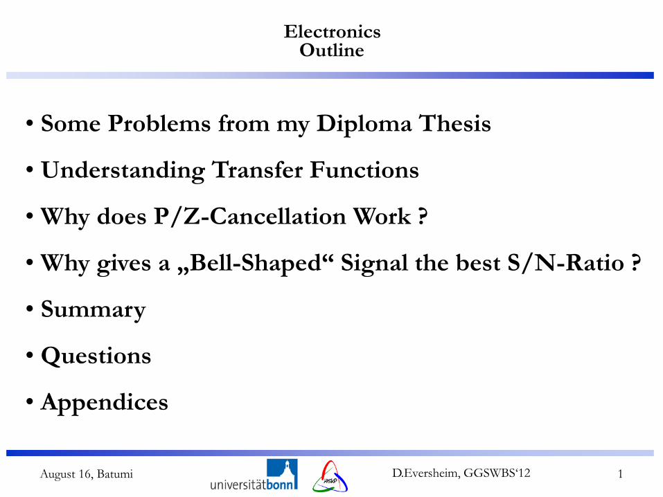
The Main Amplifier
Potentiometer reads P/Z
What does it ?
What does it mean ?
How does the circuit look like ?
How does it work ?
Electronics
August 16, Batumi D.Eversheim, GGSWBS‘12 4
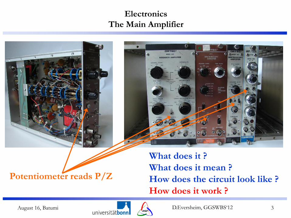
The Main Amplifier Input Stage
That is, what it means How does it work ?
Amplitude wrong by this amount
That is the circuit
That is, what it does
Electronics
August 16, Batumi D.Eversheim, GGSWBS‘12 5
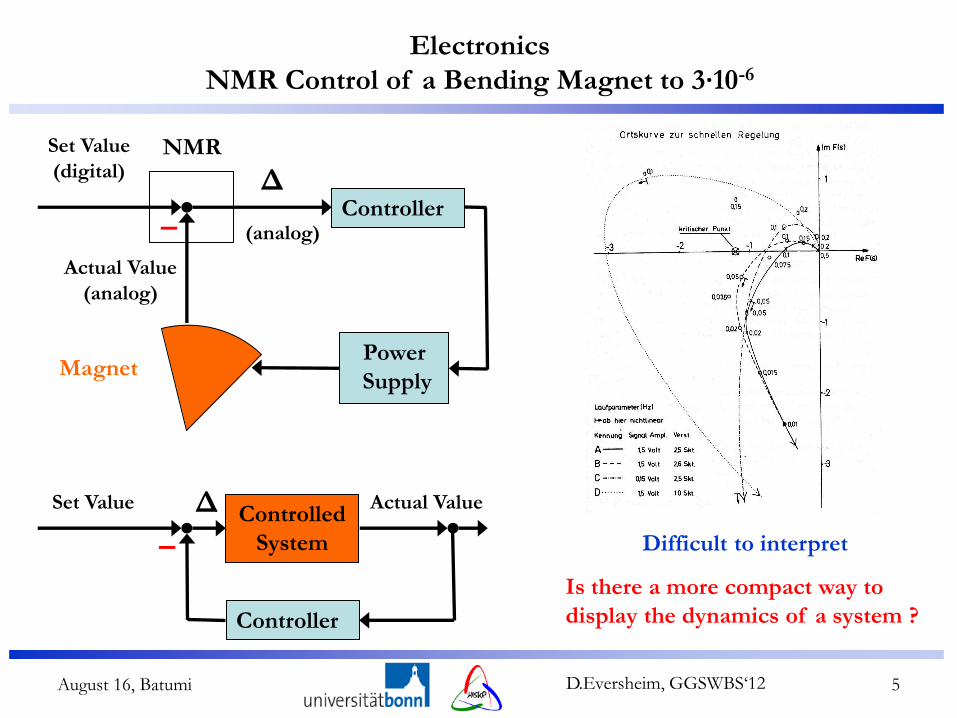
NMR Control of a Bending Magnet to 3∙10-6
Controller
Controlled
System –
Set Value Δ Actual Value
Set Value
(digital)
Actual Value
(analog)
NMR
–
Power
Supply Magnet
Δ
(analog) Controller
Difficult to interpret
Is there a more compact way to
display the dynamics of a system ?

Electronics
August 16, Batumi D.Eversheim, GGSWBS‘12 6
Understanding Transfer Functions
t
e
t
e
1
100°C -T
The temperature of a piece of metal
approaches exponetially 100°C.
UR
The voltage at the capacitor approaches
exponetially U0
• The water tank is filled from a reservoir of unlimited capacity;
• The water level approaches exponetially h0.
Water
tank
Reservoir
Wat
er lev
el h
Filling
(Rise)
Drain (Drop)
Electronics
August 16, Batumi D.Eversheim, GGSWBS‘12 7
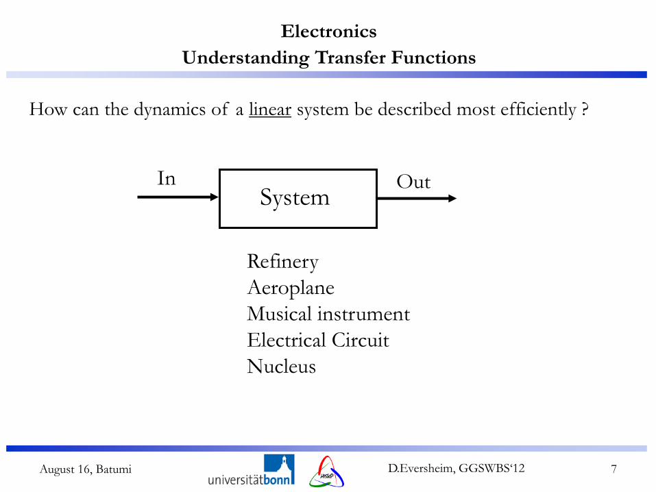
Understanding Transfer Functions
How can the dynamics of a linear system be described most efficiently ?
System In Out
Refinery
Aeroplane
Musical instrument
Electrical Circuit
Nucleus

Electronics
August 16, Batumi D.Eversheim, GGSWBS‘12 8
Understanding Transfer Functions
− Is a „generalized“ Fourier Transform f(t) F(s) with s=ρ+iω
− Is an integral transform, and therefore linear
− „Algebraizes“ linear differential equations
− A convolution in the time domain corresponds to a multiplication of
the corresponding Laplace transforms
Scheme: f(t) F(s)
h(t) H(s)
t
u)duf(u)g(t0
-1
G(s)F(s)

Electronics
August 16, Batumi D.Eversheim, GGSWBS‘12 9
Understanding Transfer Functions
F(s)
f(t) Remark
a F1(s) + b F2(s)
a f1(t)+ b f2(t) Linearity
s F(s) – f(0)
f ´(t) Derivative
sn F(s) – s
(n-1) f(0) –
– s (n-2)
f‘(0) .... – f (n-1)
(0)
f(n)
(t) n
th derivative
Integral
n-fold integral
F(s) · G(s)
Convolution in the time domain
s
sF )(
ns
sF )(
t
duuf0
)(
t
duutguf0
)()(
t t t nn duuf
n
utduuf
0 0 0
1
)()!1(
)()(...

Electronics
August 16, Batumi D.Eversheim, GGSWBS‘12 10
Understanding Transfer Functions
F(s)
f(t)
1
t
eat
cos (at)
s
1
2
1
s
,...3,2,11
nsn
as
1
22
1
as
22 as
s
22
1
as
1!0,)!1(
1
n
t n
a
atsin
a
atsinh
nQ s s sQ s
P s 1( ) ( ); .. ( )
(
)
).
( k k
k
k
nt
k k
k dQQ
Q d s
P e
1
;( )
'( )'( ) (
( )
)
Electronics
August 16, Batumi D.Eversheim, GGSWBS‘12 11
Understanding Transfer Functions
F1(s) F2(s)
T(s) = F1(s)·F2(s) (Convolution) T(s) = F1(s) ± F2(s) (Linearity)
F1(s)
F2(s)
Feedback (especially: negative feedback)
1
1 2
F (T(s) = =
1
Y(s)
X
s)
F (s)) ±( Fs (s) 2
-1
1 2
1= ± =
F (s)F (s) T(s) ±F (s)Trick:
Y(s) = F1(s)·Δ(s)
Δ(s) = X(s) R(s)
R(s) = F2(s)·Y(s)
Y(s) = F1(s) · {X(s) (F2(s)·Y(s))} F2(s)
X(s) Y(s)
R(s)
Δ(s) F1(s)
Recall: s=ρ+iω
T(s) ≝ Output(s)
Input(s)
Electronics
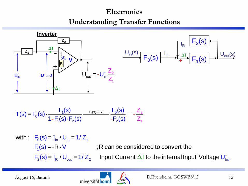
August 16, Batumi D.Eversheim, GGSWBS‘12 12
Understanding Transfer Functions
intI
I
I
-1F (s)1 0
0
1 2 2
0 in in 1
1
2 R out 2
2
1
=
with : = / =
= -R ; R can b
F (s) F (s)T(s) F (s)
1 F (s) F (s) F (s)
F (s) U 1/ Z
F (s) V
F (s)
e considered to convert the
= / = Input Current to the internal Input Voltage
--
U 1/ Z U
Z
Z
.
Inverter
inou2
1
tU =Z
-Z
U
+
Z2
Z1
-
inU
F1(s)
F2(s)
Uin(s) Uout(s) F0(s)
Iin
IR
0-U
R
-
intUV
I
I
I
Electronics
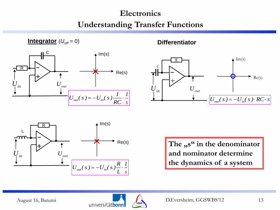
August 16, Batumi D.Eversheim, GGSWBS‘12 13
Understanding Transfer Functions
out in
1 1U ( s ) U ( s )
sRC
Integrator (Uoff = 0)
Im(s)
Re(s)
inU
C
outU+
R
Re(s)
Im(s)
out inU ( s ) U ( ss ) RC
Differentiator
inU
C
outU
+
R
out in
R 1U ( s ) U ( s )
sL
Im(s)
Re(s)
inU
L
outU+
R
The „s“ in the denominator
and nominator determine
the dynamics of a system
Electronics
August 16, Batumi D.Eversheim, GGSWBS‘12 14
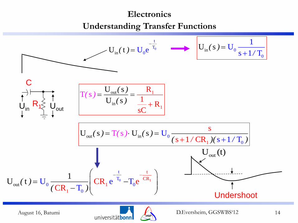
Understanding Transfer Functions
out
i
1
n1
U s
U
R
1R
sC
Ts
s( )
((
))
0
0in
t
TUU t e
( ) 0in
0
U1
Us
s1 T
)/
(
out i
01
0n Us
s s 1 TU
1 Cs
Rs T Us( ) ( )
( /( )
)( )/
10
tt
T
0 01
0
t
C
o
R
u
1
U eCR eCR
UT
1Tt
( )( )
outU (t)
Undershoot
C
R1 Uin Uout
Electronics
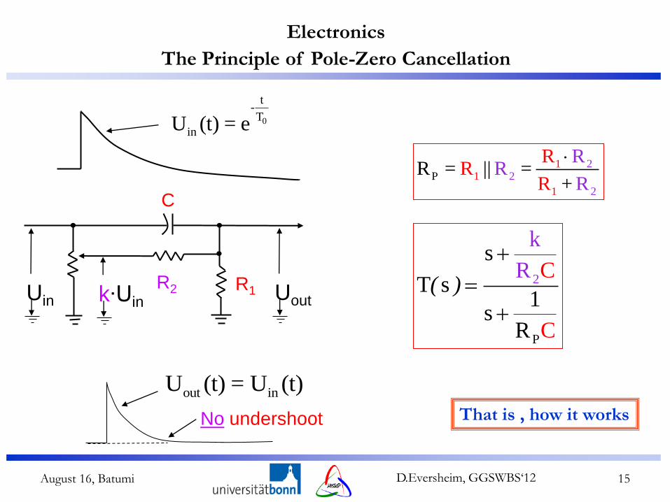
August 16, Batumi D.Eversheim, GGSWBS‘12 15
The Principle of Pole-Zero Cancellation
0
t-T
inU (t) = e
11
1
P2
2
2
R = || R
RR
R= R
+ R
2
P
k
R Cs
T s1
sR C
( )
out inU (t) = U (t)
No undershoot
C
R1 R2 k∙Uin Uin Uout
That is , how it works

Electronics
August 16, Batumi D.Eversheim, GGSWBS‘12 16
Understanding Transfer Functions
Stable Systems have Poles only in the negative half
plane (imaginary axis included), since otherwise ρ>0
Allpasses stand out due to the symmetric position of
Poles and Zeros with respect to the imaginary axis.
|T(s)| = const.; but the phase changes.
Phase minimum systems do not have any Zeros in the
right half-plane.
Inferences:
All stable linear systems
can be set up by allpasses and
phase minimum systems.
iω
ρ
iω
ρ
iω
ρ
iω
ρ
-a b -a b
Allpass Phase min.-
system
iω
ρ
Electronics
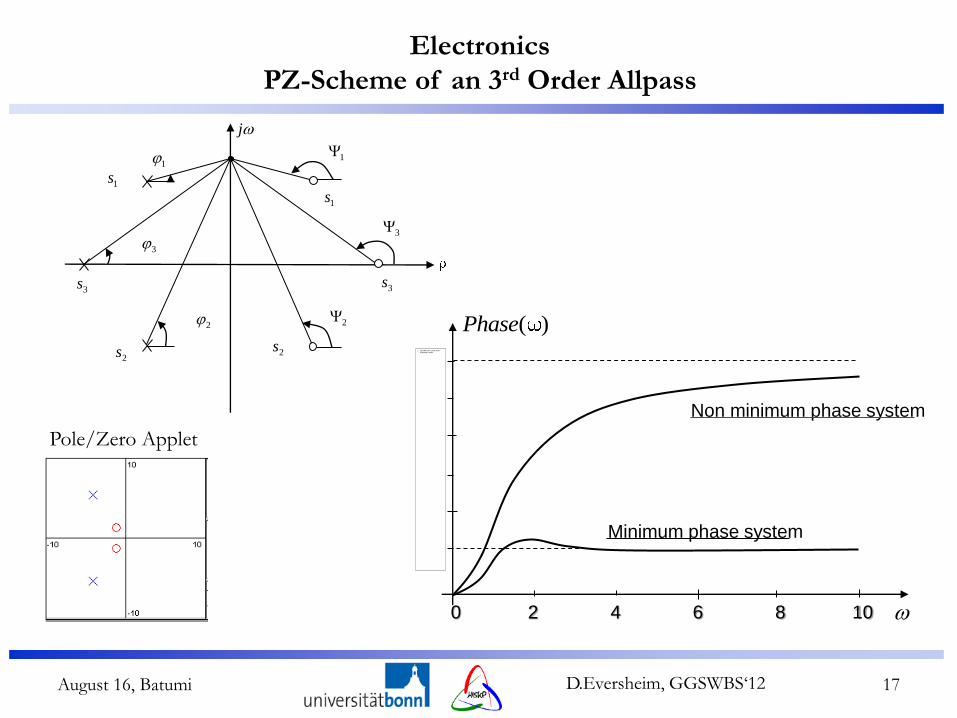
August 16, Batumi D.Eversheim, GGSWBS‘12 17
PZ-Scheme of an 3rd Order Allpass
Non minimum phase system
Minimum phase system
( )Phase
0 2 4 6 8 10
1s1s
3s 3s
2s2s
1
2
3
1
2
3
j
Pole/Zero Applet

Electronics
August 16, Batumi D.Eversheim, GGSWBS‘12 18
Pulse Shaping
2 Stage Sallen-Key
Amplifier
Electronics
August 16, Batumi D.Eversheim, GGSWBS‘12 19
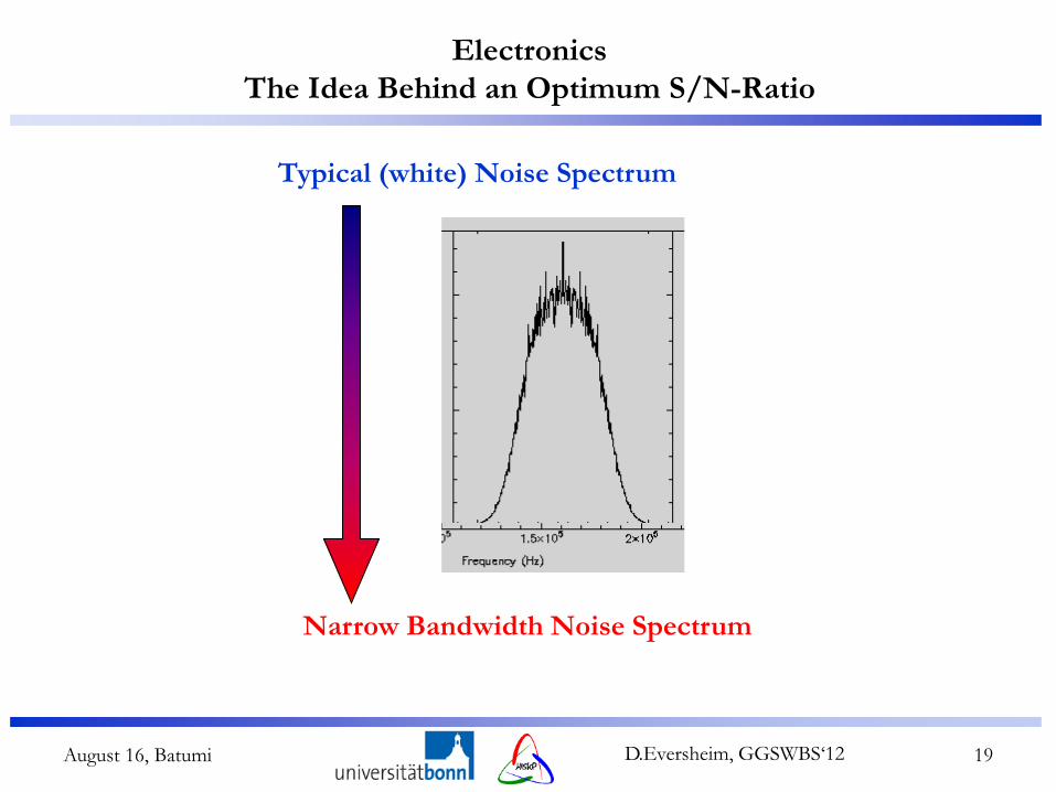
The Idea Behind an Optimum S/N-Ratio
Typical (white) Noise Spectrum
Narrow Bandwidth Noise Spectrum

Electronics
August 16, Batumi D.Eversheim, GGSWBS‘12 20
Pulse Shaping

Electronics
August 16, Batumi D.Eversheim, GGSWBS‘12 21
Pulse Shaping
Rectangle
Triangle
Parabula
Exp. RiseAndFall

Electronics
August 16, Batumi D.Eversheim, GGSWBS‘12 22
Pulse Shaping
Semi-Gaussian pulse shaping has the fewest harmonics and allows
to amplify these pulses with the comparatively smallest bandwidth.
Therefore, all noise outside this bandwidth can be suppressed.
Gauss
Lorentzian
Haversinus

Electronics
August 16, Batumi D.Eversheim, GGSWBS‘12 23
Summary
Have a wide field of applications
Are an universal tool to handle even aperiodic signals
Give a very basic understanding of systems
Allow to evaluate or predict the dynamical behavior
of a system
Transfer Functions:

Electronics
August 16, Batumi D.Eversheim, GGSWBS‘12 24
You can find further informations (and much more):
www.hiskp.uni-bonn.de
Archive → my lectures
User: student
PW: SSXX
WSXX

Electronics
August 16, Batumi D.Eversheim, GGSWBS‘12 25
Questions
–– Give two reasons why the P/Z
circuit is termed „principal“.
C
R1 R2 k∙Uin Uin Uout
–– Convince yourself „graphically“ that the amplitude
of an Allpass does not depend on frequency.
iω
ρ
–– Does the „trick“ of linearizing (in negative feedback systems) apply
only to operational amplifiers ?

Electronics
August 16, Batumi D.Eversheim, GGSWBS‘12 26
The Preamplifier
CQU inout /
Q/U Converter
inQ C
+
Q=C U
The output voltage is changed, until the charge via C compensates
Qin from the input

Electronics
August 16, Batumi D.Eversheim, GGSWBS‘12 27
Appendix A1 (Backtransform)
out i
01
0n Us
s s 1 TU
1 Cs
Rs T Us( ) ( )
( /( )
)( )/
Electronics
August 16, Batumi D.Eversheim, GGSWBS‘12 28
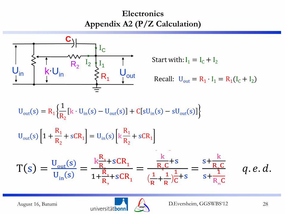
Appendix A2 (P/Z Calculation)
C
R1
R2 k∙Uin
Uin Uout
I1
IC
I2

Electronics
August 16, Batumi D.Eversheim, GGSWBS‘12 29
Appendix A3 (P/Z Circuit Considerations – Reality)
2
P
k
R Cs
T s1
sR C
( )
But since k is always a fraction of 1 this constitutes a contradiction.
+ _
Solution:
Electronics
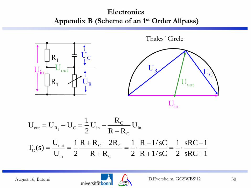
Appendix B (Scheme of an 1st Order Allpass)
Uout Uin
R1
R1 UC
UR
Uin
UR UC
Uout
Thales´ Circle
1
Cout R C in in
C
out C CC
in C
R1U U U U U
2 R R
U R R 2R1 1 R 1/ sC 1 sRC 1T (s)
U 2 R R 2 R 1/ sC 2 sRC 1
August 16, Batumi D.Eversheim, GGSWBS‘12 30
Electronics
August 16, Batumi D.Eversheim, GGSWBS‘12 31
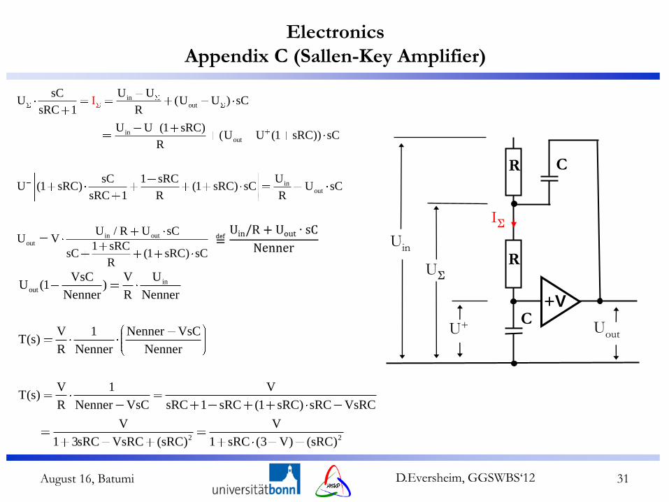
Appendix C (Sallen-Key Amplifier)
inout
inout
inout
in outout
sC U UU (U U ) sC
sRC 1 R
U U (1 sRC)(U U (1 sRC)) sC
R
sC 1 sRC UU (1 sRC) (1 sRC) sC U sC
sRC 1 R R
U / R U sCU V
1 sRCsC (1 sRC) sC
R
I
inout
2 2
VsC V UU (1 )
Nenner R Nenner
V 1 Nenner VsCT(s)
R Nenner Nenner
V 1 VT(s)
R Nenner VsC sRC 1 sRC (1 sRC) sRC VsRC
V V
1 3sRC VsRC (sRC) 1 sRC (3 V) (sRC)
C
R U
Uin
Uout
+V
C R
U+
I

Electronics
August 16, Batumi D.Eversheim, GGSWBS‘12 32
Appendix D (Nonlinear Systems)
Given:
Set of m non-linear differential equations:
y f (x,u) with : x n Var iables
u Parameters
Expand f for the (operating) point A:
A A
|A |A
m x matrixm x n matrix
f fy f (x ,u ) x u Higher order terms; m n
x u
A Af(x , u ) + δx + δu
GF
F G
This is a system of coupled linear differential equations, which can be
algebraized by means of the Laplace transform.
≈
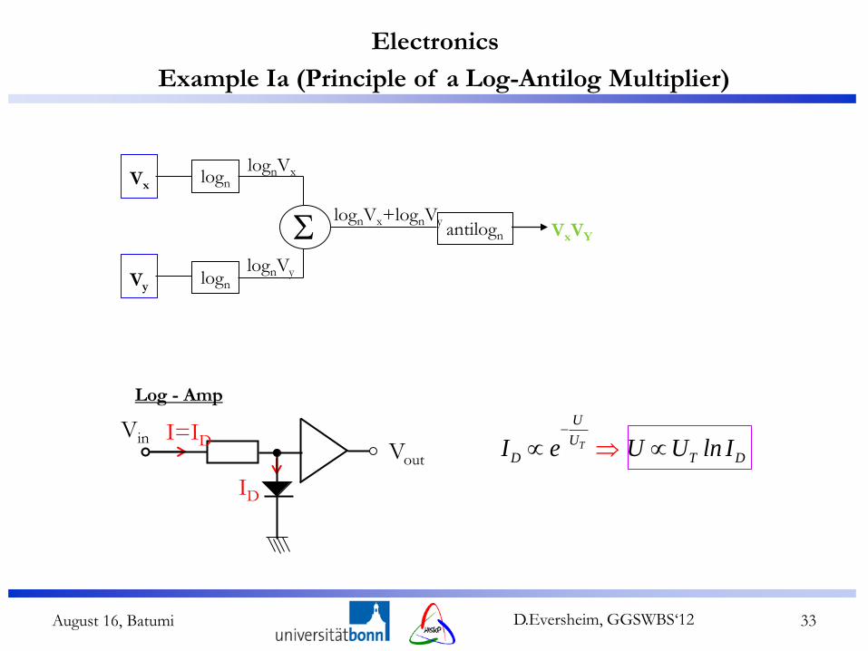
Electronics
logn
logn
antilogn
lognVx
lognVy Vy
Vx
lognVx+lognVy VxVY
Log - Amp
T
U
U
D T DI e U U ln I
Vin I=ID
ID
Vout
Example Ia (Principle of a Log-Antilog Multiplier)
August 16, Batumi D.Eversheim, GGSWBS‘12 33

Electronics
F s
F sT s
F s G s
F s G s
( )
( )( )
1 ( ) ( )
1
1 / ( ) ( )
-11/G(s) = G (s)
Carrier frequency:
Modulated signal:
Output (Modulated carrier):
Vx
Vy
VxVy
Example of an analog multiplier: Amplitude modulation
LOG
AMP
VIN VOUT
VIN = LOGA (VOUT)
AV(in) = VOUT
Example Ib (Principle of a Log-Antilog Multiplier)
Log Amp as a negative feedback element
results in a Anti-Log-Amplifier:
August 16, Batumi D.Eversheim, GGSWBS‘12 34

Electronics
Example IIa (Principle of a Sonar)
t2
t3 t4
~ ~ ~
t1
Δt
Δt = t4-t1
Allpass-1
Allpass
Unfortunately this does not work!
t3
t4
August 16, Batumi D.Eversheim, GGSWBS‘12 35

Electronics
Principle of the CPA : High peak intensities within the amplifier optics are avoided by
timewise and spatial dilatation of the pulses.
fs-Oscillator Stretcher
Regenerative
amplifier
Compressor
fs-
Puls
Example IIb (Chirped Pulse Amplification (CPA))
August 16, Batumi D.Eversheim, GGSWBS‘12 36

Electronics
R(s)
S(s)
Distortion Set Value
V Controlled
System
Controller
UA UE
VV V S ST s S
V R V R R
( )
1 1
the dynamics of T(s) can be determined by the position of the Pole/Zero-distribution of
R(s).
Example III (Linearizing Systems)
August 16, Batumi D.Eversheim, GGSWBS‘12 37