Embed Size (px)
Citation preview

SOLID STATE ELECTRONICS DIGITAL ELECTRONICS SOFT CONDENSED MATTER PHYSICS

PHYSICS
The energy band occupied by the valence
electrons is called valence band and is the
highest filled band.
Bnd occupied by the electrons coming from
the valence band is called conduction band. It
is either empty or partially filled and lies above
the valence band.
The minimum energy required by an electron
to jump from valance band to conduction band
is equal to the forbidden energy gap.
B

• Conductors:In conductors the valence and
conduction band overlap on each other
such that forbidden energy gap is not
there.The electrons in the overlapping
region are called conduction electrons.
• Insulator:In insulators the valence band is
completely filled and conduction band is
empty and both bands are separated by a
forbidden energy gap of 7eV.
PHYSICS

PHYSICS •Semiconductor: semiconductors are the
materials in which the forbidden energy gap
between valence and conduction band is very
small.
•Examples are germanium(Eg=0.72eV) and
silicon(Eg=1eV).
•The pure semiconductors are called intrinsic
semiconductor where as those having some
specific impurity are called extrinsic
semiconductor.
• the process of adding impurities to
semiconductors is called doping.
•2 types of impurities are pentavalent

• The pure semiconductors are called
intrinsic semiconductor where as those
having some specific impurity are called
extrinsic semiconductor.
PHYSICS

• The pure semiconductors are called
intrinsic semiconductor where as those
having some specific impurity are called
extrinsic semiconductor.
PHYSICS

• n type semiconductor: when pentavalent impurity is added to pure germanium or silicon crystal we get an extrinsic semiconductor known as n type semiconductor.
• p type semiconductor: when trivalent impurity is added to pure germanium or silicon we get p type semiconductor The boundary dividing the two halves of such a semiconductor is called a junction and the arrangement is known as p n junction diode.
PHYSICS

• The region around the junction containing immobile +ve and –ve charges is known as depletion region.
• Symbol of diode:
• When a battery or emf greater than the barrier potential is connected in such a way that +ve terminal is connected to p side and –ve terminal of battery is connected to n side the diode is said to be in forward bias condition.
PHYSICS

Diode as half wave rectifier:
f
PHYSICS

• Diode as full wave rectifier:
f
PHYSICS
During +Ve half cycle
During -Ve half cycle

• Junction transistor is a 3 terminal Semiconductor. It is formed when a thin layer of one type of extrinsic semiconductor is sandwitched between 2 thick layers of other type of extrinsic semiconductor.
• 2 Types namely npn and pnp whose symbols are as shown…
PHYSICS

• An intermediate state structure called liquid crystal appears b/w the crystalline solid state at low temperature and the ordinary liquid state at high temperature.
• gel:dispersion medium is solid,dispersed phase is liquid.
• An emulsion is a colloidal dispersion in which 2 immisible liquids are used as dispersed phase and dispersed medium
PHYSICS

• Boolean algebra:this algebra allows only 2 states for a variable.these states are represented as high (1) or low(0).
• The OR operation is represented as y= a+b =a OR b
• The AND operation is represented as y=a AND b=a.b
• The NOT operation is y=NOT a
PHYSICS

• NAND,NOR gate are called universal logic gates.which are complementery operation of AND and OR respectively.
• Half adder is logic circuit which adds 2 bits at a time.
• Full adder is a circuit which adds 3 bits at a time.
PHYSICS

The bands in which an
electron cannot lie in a
crystal
1. Valence band
2. Forbidden band
3. Conduction band
4. In all energy bands
PHYSICS

f
Answer (2)
PHYSICS

The conduction electrons have greater mobility than that of holes because
1) They are lighter
2) They carry –ve charge
3) Need less energy for movement
4) Experience less collision
PHYSICS

Answer (3)
PHYSICS

A piece of copper and germanium are cooled
from room temperature to 100K. What
happens to their resistivity?
1) Decreases in both
2) Increases in both
3) Increases in copper & decreases in
germanium
4) Decreases in copper & increases in
germanium
PHYSICS

Temperature coefficient for copper
is positive and that for germanium
is negative.
Answer (4)
PHYSICS

In the depletion region of p-n
junction there is a shortage of…..
1) Acceptor ions
2) Donor ions
3) Holes and electrons
4) None of the above
PHYSICS

Answer (3)
PHYSICS

At room temperature an
intrinsic semiconductor has…
1. Many free electrons only
2. A few free electrons and holes
3. No free electrons and holes
4. Many holes only
PHYSICS

Answer (2)
PHYSICS

For a transistor the α and β
values are as follows….
1) αβ=1
2) α<1 and β>1
3) α>1 and β<1
4) None of the above
PHYSICS

Answer (2)
PHYSICS
p-n junction diode acts as insulator. if
connected......
1) In reverse bias
2) To ac source
3) In forward bias
4) Either to ac source or in reverse
bias
PHYSICS

In reverse bias condition depletion
region increases resulting in the
increase of resistance.
Answer (1)
PHYSICS

Which type of liquid crystals used to
prepare holograms ?
1.Cholesteric
2.Smectic A
3.Smectic C
4.Nematic
PHYSICS

Answer (1)
PHYSICS

Half adder is the combination of
the following
1) AND and XOR gates
2) AND and OR gates
3) XOR and NOT gates
4) XOR and OR gates
PHYSICS
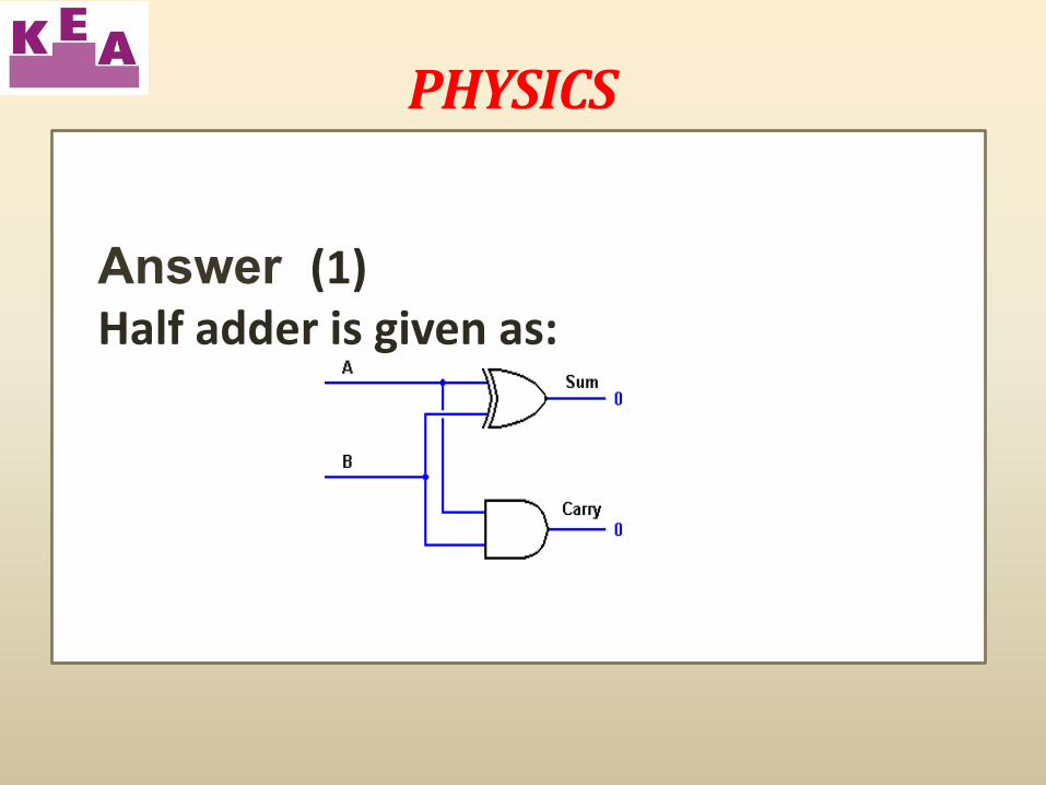
Answer (1) Half adder is given as:
PHYSICS

Which of the following is not
the function of NOT gate
1) Complement signal
2) Stop a signal
3) Invert an input signal
4) Change the logic level of the digital circuit
PHYSICS

Answer (2) The output of NOT gate is ‘1’ when input is ’0’,when input is ‘0’ output is ’1‘.Hence except (2) all answers are correct.
PHYSICS

In a transistor the base is...
1) An insulator
2) An extrinsic semiconductor
3) A conductor of high resistance
4) A conductor of low resistance
PHYSICS

Answer (2)
PHYSICS

The energy band gap between conduction band and the valence band in a material is 0.7eV . It is....
1) A metal
2) An insulator
3) An alloy
4) A semiconductor
PHYSICS

Answer (4) Energy gap of semiconductor is approximately 1eV.
PHYSICS

A colloidal state in which a gas is
dispersed in a liquid or a solid is….
1) gel
2) Liquid crystal
3) foam
4) emulsion
PHYSICS

Answer (3)
PHYSICS

The main distinction between
conductors, semiconductors and
insulator is …
1)Binding energy of electrons
2)Work function
3)Width of forbidden band
4)Temperature coefficient of
resistance
PHYSICS
Answer (3)
PHYSICS

The Boolean equation for the
given logic circuit is
1) Y=a AND b
2) Y=a OR b
3) Y=a XOR b
4) Y=a NAND b
PHYSICS
a b Y
Answer (1)
PHYSICS

In which of the following cases the diode is
forward biased…
PHYSICS

Answer (4)
PHYSICS

Minority carriers present in a p- type semi
conductor are due to
1. Bias voltage
2. Thermal agitation
3. Addition of impurities
4. Ionisation of impurities
PHYSICS
Answer(2)
PHYSICS

A Nematic liquid crystalline phase
has..
1) Position order only
2) Orientational order only
3)Both Orientational and positional order
4) All the above
PHYSICS

Answer (2)
PHYSICS

The reverse biasing in a
junction diode… 1)Decreases the potential barrier
2)Increases the potential barrier
3)Increases the number of minority charge
carriers
4) Increases the number of majority charge
carriers
PHYSICS

Answer (2)
PHYSICS

Phase angle between input and output
signals in a CE amplifier in degrees is…
1. 180
2. 45
3. 90
4. 0
PHYSICS

Answer (1)
In CE amplifier we take output across the emitter. Hence output and input signals differ by a value of 180 degrees
PHYSICS
In which of the following states of
matter the majority of crystalline
substances generally exist?
1) liquid
2) solid
3) foam
4) plasma
PHYSICS

Answer (2)
PHYSICS

When the conductivity of a
semiconductor is only due to the
breaking of covalent bond ,then the
semiconductor is…
1. Extrinsic
2. Donor
3. intrinsic
4. acceptor
PHYSICS

Answer (3)
PHYSICS

To a germanium crystal equal
number of aluminium and arsenic
atoms are added. Then.…..
1) It becomes an insulator
2) It remains as intrinsic
semiconductor
3) It becomes a superconductor
4) All the above
PHYSICS

Answer (2)
PHYSICS

Which of the following is called
universal gate….
1) AND
2) OR
3) XOR
4)NAND
PHYSICS

Answer (4) NAND, gate is called universal gate because any basic gate can be constructed using above gate.
PHYSICS

Identify the logic operation performed
by the circuit shown.
1) OR
2) AND
3) NAND
4) NOT
PHYSICS

Answer (3) put 1, 1 for A and B Gate 1 gives 0 Gate 2 gives 0 Gate 3 gives 1 Thus 1 is given to last NOR gate to get Q=0.Thus the given system behaves as NAND gate.
1
2
3
PHYSICS

Milk is emulsion in which…
1) Fat is dispersed medium, water is
dispersion medium
2) Both fat and water are dispersed
medium
3) Water is dispersed medium, fat is
dispersion medium
4) None of the above
PHYSICS

Answer (1)
PHYSICS

Hole in a p-type semiconductor is
….
1) An excess electron
2) A missing atom
3) A missing electron
4) A donor level
PHYSICS

Answer (3)
PHYSICS

Which of the following is the
operation of NOR gate…..
1) 1 NOR 1=0
2) 1 NOR 0=1
3) 0 NOR 0=0
4) None of the above
PHYSICS

Answer (1)
PHYSICS

True statement for AND gate is
1) It has no equivalent to switching circuit
2) It is equivalent to series switching
circuit
3) It is equivalent to parallel switching circuit
4) None of the above
PHYSICS

Answer(2)
PHYSICS

The forbidden energy band gap in conductors, semiconductors and insulators are E1,E2,E3 respectively..then which relation is true...
1) E1=E2=E3
2) E1<E2<E3
3) E1>E2>E3
4) E1<E2>E3
PHYSICS

Answer (2)
PHYSICS

A half wave rectifier is being used to
rectify an ac voltage of frequency
50Hz.The number of pulses of rectified
current obtained in 1 second is....
1) 50
2) 100
3) 25
4) 150
PHYSICS

Answer (1)
PHYSICS

A transistor has α = 0.99.then
β is…..
1)0.95
2)1.5
3)19
4)25
PHYSICS

We have the relation β=α/(1- α)
for the given question
0.95/(1- 0.95) =19
Answer (3)
PHYSICS

What is the final output of given logic
circuit, if the input for first 2 NAND
gates is ‘1’....
1. ‘1’
2. ‘0’
3. ‘0’ or ‘1’
4. Not possible
to say
PHYSICS

1 Answer (2)
PHYSICS
1
1
1
0 1
0
1 0

The truth table shown here
belongs to which of the
following logic gates…
1) NOR
2) OR
3) AND
4) XOR
PHYSICS

Since the output is ‘0’ for same combination Of input and is ‘1’ for different combination ,it Is the truth table of XOR gate.
Answer (4)
PHYSICS

At 0K ,intrinsic semiconductor
behaves as...
1) A perfect conductor
2) A perfect insulator
3) A semiconductor
4) A super conductor
PHYSICS

Answer (2)
PHYSICS

What is the output expression for
given logic circuit......
1)(A+B)+BC
2) (B+C) A
3)AC+BC
4)AC(B+A)
PHYSICS

Answer (1)
PHYSICS

Which of the following when added as
a impurity to the silicon produces the
n type semiconductor…?
1)P
2)Al
3)Mg
4)B
PHYSICS

Answer (1)
PHYSICS

One serious drawback of
semiconductor devices is...
1. They do not last for long time
2. They pollute the environment
3. They are costly
4. They can’t be used with high
voltages
PHYSICS

Answer (4)
PHYSICS

PHYSICS
The electrical circuits used to
get smooth DC from rectifier
circuit is…
1. Full wave rectifier
2. Amplifier
3. Oscillator
4. filter

Answer(4)
PHYSICS

If l1, l2 and l3 are the lengths of the emitter , base and collector of a transistor then
1. l3 < l2>l1
2. l3 =l2=l1
3. l3 >l1>l2
4. l3 <l1<l2
PHYSICS

Answer(3)
PHYSICS

THANK YOU
PHYSICS