Embed Size (px)
Citation preview
I n t e r n a t i o n a l
SoC DesignConference
InternationalSoC Design Conference
2 0 0 5
http://www.isocc.org
I ∙ S ∙ O ∙ C ∙ C ∙ 2 ∙ 0 ∙ 0 ∙ 5
I ∙ S ∙ O ∙ C ∙ C ∙ 2 ∙ 0 ∙ 0 ∙ 5
Hosted bySoC Design Technical Society
IEEK (The Institute of Electronics Engineers of Korea)
Organized bySemiconductor Society, IEEK
IDEC (IC Design Education Center)
COEX Conference Center, Seoul, Korea
October 20-21, 2005

16 17
http://ww
w.isocc.org
2005 International SoC
Design
Conference
http://ww
w.isocc.org
2005 International SoC
Design
Conference
Friday, 21 October
Room 321
Registration
Coffee Break
Lunch
(Room 321)
Santa Cruz)
Keynote Speech ⅢSung-Mo Kang
(University of California,
Session 10
Session 15
Invited Talk ⅣNobuyuki
Nishiguchi(STARC)
Tutorial ⅣHyun-Kyu Yu
(ETRI)
MEMS
Video/AudioSignal
Processing Ⅲ
EmbeddedMemory
Display Driverand lmaging
Devices
SoC Testing andVerification Ⅱ
Coffee Break Coffee Break
Session 19
RF, Analog& Mixed-Signal
Circuit Ⅲ
Communicationand NetworkProcessor
SoC DesignMethodology Ⅴ
Low PowerDesign
Techniques Ⅱ
Session 20 Session 21
Session 16 Session 17 Session 18
Tutorial ⅢDavid A Rusling(ARM Fellow)
SoC DesignMethodology Ⅳ
RF, Analog & Mixedl-Signal
Circuit Ⅱ
Signal Intergrityand
InterconnectModeling
High SpeedSignal
Interface
Chip DesignContestSession
(10:00~16:50)
PosterSession B
(13:00~16:00)
Invited Talk ⅢMartin D. F. Wong(University of lllinois)
Session 11 Session 12 Session 13 Session 14
Room 330 A, B Room 311 A, B Room 330 C Room 311 C Room 320 Lobby
08:00~09:00
09:30~10:50
10:50~11:10
11:10~12:00
12:00~13:00
13:00~14:50
14:50~15:10
15:10~16:50
16:50~17:10 (Room 321)Closing Ceremony

61
http://ww
w.isocc.org
2005 International SoC
Design
Conference
Jaewon Cha, Euncheol Lee, Kyosun Kim,
Department of Electronic Engineering,
University of Incheon
� A 6-bit(3+3) segmented Current-Steering CMOS
D/A Converter for UWB
Tae-kyu Nam, Sang-wook Park, Sung-min Ha,
Sung-wook Seo, Kwang-sub Yoon, Department
of Electronic Engineering, Inha University
� VLSI Implementation of Multilevel Lifting based
Discrete Wavelet Transform for JPEG2000
Gab Cheon Jung, Hyoung Jin Moon, Hong
Bum Son, Seong Mo Park, Department of
Electronics Engineering, Chonnam National
University
� Radix-2 to the 4th Power 1024 Point Pipeline
FFT Processor Using a Data Scaling Approach
Jung-Yeol Oh*, Eun-Kwang Ryu, Sun-Ah Hong,
Myoung-Seob Lim, Division of Electronics and
Information Engineering, Chonbuk National
University, *Electronics and Telecommunications
Research Institute
� A Crypto-Processor for Security PDA Systems
Jinsub Park, Yeonsang Yun, Seungyoul Kim,
Young-Dae Kim, Younggap You, School of
ECE, CBNU
� A 32/16 Multi-Phase Delay-Locked Loop for
DVD Application
Hyungjoon Chi, Seungjun Bae, Hongjune Park,
Jihyun Kim*, Jaeyup Lee*, Heesub Lee*,
Department Electronics Engineering, Pohang
University of Science and Technology, *DMA
60
http://ww
w.isocc.org
2005 International SoC
Design
Conference
University, *Power Telecommunication
Network Group, Korea Electrotechnology
Research Institute
� Interpolating-Gated-Oscillator CDR
Du-ho Kim, Pyung-su Han, Woo-Young Choi,
Department of Electrical and Electronic
Engineering, Yonsei University
� A 1.25Gb/s Clock and Data Recovery Circuit
for Multi-channel Application
Chang-kyung Seong, Seung-woo Lee*, Woo-
young Choi, Department of Electrical and
Electronic Engineering, Yonsei University,
Switching Technology Team, Electronics and
Telecommunications Research Institute
� SMART7F : A Reusable Design of 32-bit RISC
Core for Embedded Applications
Dong-hoon Yang, Seung-ho Kwak, Moon-key
Lee, Department of Electronic Engineering,
Yonsei University
� A Digital 120Mb/s MIMO-OFDM Baseband
Processor for High Speed Wireless LANs
Yunho Jung, Jiho Kim, Seungpyo Noh,
Seongjoo Lee, Jaeseok Kim, Department of
Electrical and Electronic Engineering, Yonsei
University
� ASK modulator and Antenna driver for
13.56MHz RFID Interrogators
Jung-Hyun Cho, Kyung-Won Min, Haksu Kim*,
Shiho Kim*, School of Electronics and Electrical
Engineering, Wonkwang University, *School of
Electrical and Computer Engineering,
Chungbuk National University
� The Fastest Single-Layer Robust QCA Adder ‘*’ indicates a best paper award candidate

Interpolating-Gated-Oscillator CDR
Du-ho Kim, Pyung-su Han and Woo-Young Choi Department of Electrical and Electronic Engineering
Yonsei University Seoul, Korea
Abstract – If there is the duty cycle distortion, the performance of the burst-mode link using clock and data recovery circuit (CDR) based on gated-oscillators is seriously degraded by the duty cycle distortion. In this paper, we demonstrate a novel gated- oscillator CDR structure which can eliminate the effect of the duty cycle distortion.
Keywords: burst-mode CDR, duty cycle distortion, gated oscillator, phase interpolator.
1 Introduction The clock recovery circuit (CDR) based on the gated oscillator(GO-CDR[1]) is used in burst-mode applications for its instantaneous locking capability. Commonly used CDRs using tracking algorithm (e.g. PLL) are not suitable for the burst mode applications, because the tracking time is usually too long.
Figure 1. Effect of duty cycle distortion
Figure 2. Block diagram for IG-CDR
Suppose that there is the duty cycle distortion in input data as shown in Fig. 1. The duty cycle distortion is transferred to the recovered clock as shown in Fig. 1. Such clock signals cannot be used in other signal processing blocks. In addition, receiver BER can increase since sampling points (falling edges in clock for Fig. 1) for data retiming are not placed at the center of the data bit. Consequently, additional circuit techniques that can compensate this distortion must be considered.
2 IG-CDR The full structure of the proposed CDR is shown in Fig. 2. The interpolating-gated-oscillator-based CDR(IG-CDR) uses two outputs of the reset signal generator[2] as the enable signal for each gated oscillator and the final
clock is realized with a half phase interpolator instead of an OR gate.
Fig. 3 shows the schematic waveform of IG-CDR. The first gated oscillator resets its phase at the rising edge of the input data, and the second gated oscillator resets its phase at the falling edge of the input data. Then, the half phase interpolator sums them. This new clock is not distorted by duty cycle distortion, and the BER doesn’t increases because the sampling point (the rising edge of the recovered clock in this figure) is placed in the center of the data bit.
GO-CDR doesn’t need pre-amble because it always resets the phase at all data transitions. But IG-CDR needs the rising edge and the falling edge to reset the phase of each gated oscillator. So, IG-CDR needs two pre-amble bits, e.g. ‘1 0’.
Figure 3. Operation of IG-CDR
* This work was supported by IDEC, Hynix 0.35 ㎛ and the Ministry of Science and Technology of Korea and the Ministry of Commerce, Industry and Energy through the System IC 2010 program
3 Measurement Results
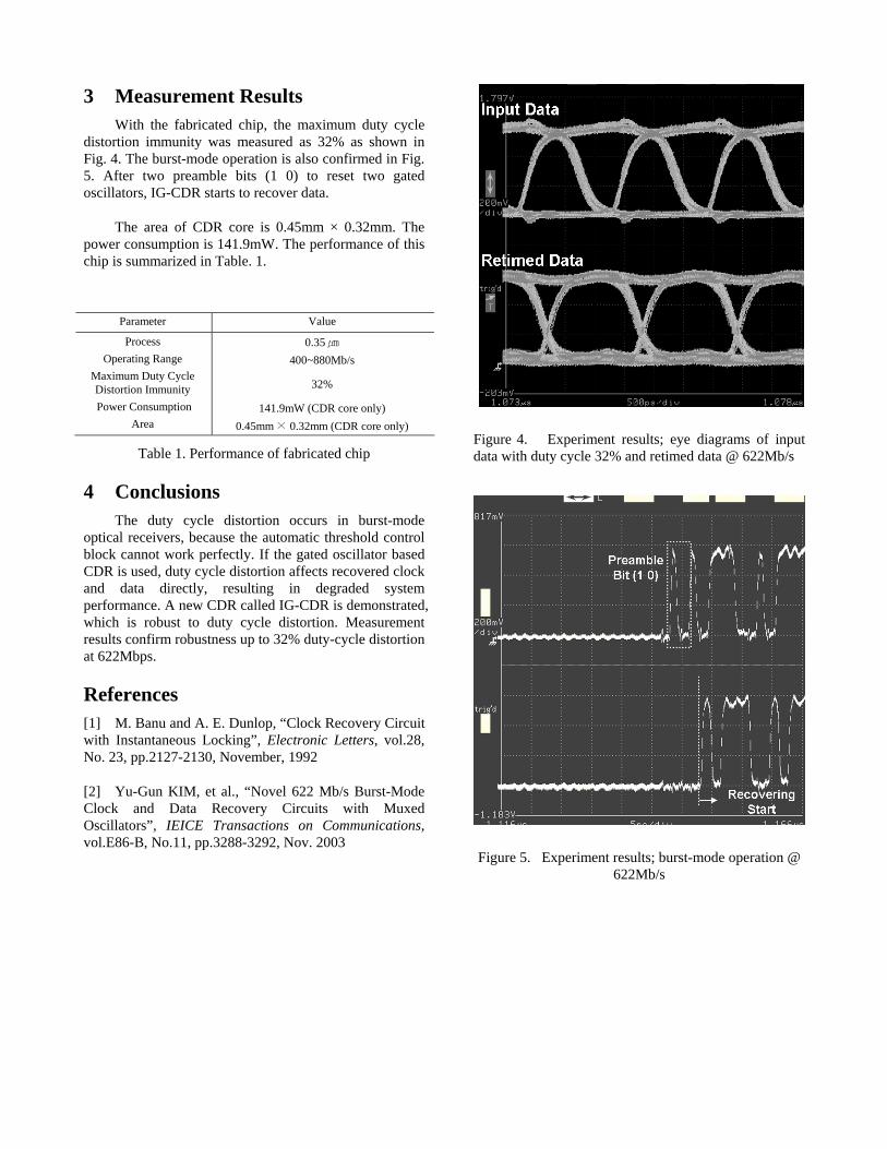
Figure 4. Experiment results; eye diagrams of input data with duty cycle 32% and retimed data @ 622Mb/s
With the fabricated chip, the maximum duty cycle distortion immunity was measured as 32% as shown in Fig. 4. The burst-mode operation is also confirmed in Fig. 5. After two preamble bits (1 0) to reset two gated oscillators, IG-CDR starts to recover data.
The area of CDR core is 0.45mm × 0.32mm. The power consumption is 141.9mW. The performance of this chip is summarized in Table. 1.
Parameter Value
Process Operating Range
Maximum Duty Cycle Distortion Immunity Power Consumption
Area
0.35 ㎛ 400~880Mb/s
32%
141.9mW (CDR core only) 0.45mm × 0.32mm (CDR core only)
Table 1. Performance of fabricated chip
4 Conclusions
Figure 5. Experiment results; burst-mode operation @ 622Mb/s
The duty cycle distortion occurs in burst-mode optical receivers, because the automatic threshold control block cannot work perfectly. If the gated oscillator based CDR is used, duty cycle distortion affects recovered clock and data directly, resulting in degraded system performance. A new CDR called IG-CDR is demonstrated, which is robust to duty cycle distortion. Measurement results confirm robustness up to 32% duty-cycle distortion at 622Mbps.
References [1] M. Banu and A. E. Dunlop, “Clock Recovery Circuit with Instantaneous Locking”, Electronic Letters, vol.28, No. 23, pp.2127-2130, November, 1992
[2] Yu-Gun KIM, et al., “Novel 622 Mb/s Burst-Mode Clock and Data Recovery Circuits with Muxed Oscillators”, IEICE Transactions on Communications, vol.E86-B, No.11, pp.3288-3292, Nov. 2003