Embed Size (px)
Citation preview

LM185-1.2-N, LM285-1.2-N, LM385-1.2-N
www.ti.com SNVS742E –JANUARY 2000–REVISED APRIL 2013
LM185-1.2-N/LM285-1.2-N/LM385-1.2-N Micropower Voltage Reference DiodeCheck for Samples: LM185-1.2-N, LM285-1.2-N, LM385-1.2-N
Careful design of the LM185-1.2-N has made the1FEATURES
device exceptionally tolerant of capacitive loading,2• ±1% and 2% Initial Tolerance making it easy to use in almost any reference• Operating Current of 10μA to 20mA application. The wide dynamic operating range allows
its use with widely varying supplies with excellent• 1Ω Dynamic Impedanceregulation.• Low Temperature CoefficientThe extremely low power drain of the LM185-1.2-N• Low Voltage Reference—1.235Vmakes it useful for micropower circuitry. This voltage
• 2.5V Device and Adjustable Device Also reference can be used to make portable meters,Available regulators or general purpose analog circuitry with
• LM185-2.5 Series and LM185 Series, battery life approaching shelf life.respectively Further, the wide operating current allows it to
replace older references with a tighter tolerance part.DESCRIPTION
The LM185-1.2-N is rated for operation over a −55°CThe LM185-1.2-N/LM285-1.2-N/LM385-1.2-N areto 125°C temperature range while the LM285-1.2-N ismicropower 2-terminal band-gap voltage regulatorrated −40°C to 85°C and the LM385-1.2-N 0°C todiodes. Operating over a 10μA to 20mA current70°C. The LM185-1.2-N/LM285-1.2-N are available inrange, they feature exceptionally low dynamica hermetic TO package and the LM285-1.2-N/LM385-impedance and good temperature stability. On-chip1.2-N are also available in a low-cost TO-92 moldedtrimming is used to provide tight voltage tolerance.package, as well as SOIC and SOT-23.Since the LM185-1.2-N band-gap reference uses only
transistors and resistors, low noise and good longterm stability result.
CONNECTION DIAGRAM
Figure 1. T0-92 Package (LP)(Bottom View)
Figure 3. SOIC Package
* Pin 3 is attached to the Die Attach Pad(DAP) and should be connected to Pin 2 orleft floating.
Figure 2. SOT-23
Figure 4. TO Package (NDV)(Bottom View)
1
Please be aware that an important notice concerning availability, standard warranty, and use in critical applications ofTexas Instruments semiconductor products and disclaimers thereto appears at the end of this data sheet.
2All trademarks are the property of their respective owners.
PRODUCTION DATA information is current as of publication date. Copyright © 2000–2013, Texas Instruments IncorporatedProducts conform to specifications per the terms of the TexasInstruments standard warranty. Production processing does notnecessarily include testing of all parameters.

LM185-1.2-N, LM285-1.2-N, LM385-1.2-N
SNVS742E –JANUARY 2000–REVISED APRIL 2013 www.ti.com
These devices have limited built-in ESD protection. The leads should be shorted together or the device placed in conductive foamduring storage or handling to prevent electrostatic damage to the MOS gates.
ABSOLUTE MAXIMUM RATINGS (1) (2) (3)
Reverse Current 30mA
Forward Current 10mA
Operating Temperature Range (4)
LM185-1.2-N −55°C to +125°C
LM285-1.2-N −40°C to +85°C
LM385-1.2-N 0°C to 70°C
ESD Susceptibility (5) 2kV
Storage Temperature −55°C to +150°C
Soldering Information
TO-92 package: 10 sec. 260°C
TO package:10 sec. 300°C
SOIC and SOT-23 Pkg.
Vapor phase (60 sec.) 215°C
Infrared (15 sec.) 220°C
See AN-450 “Surface Mounting Methods and Their Effect on Product Reliability” for other methods of soldering surface mount devices.
(1) Absolute Maximum Ratings indicate limits beyond which damage to the device may occur. Operating Ratings indicate conditions forwhich the device is intended to be functional. For specifications and test conditions, see the Electrical Characteristics. The specificationsapply only for the test conditions listed.
(2) Refer to RETS185H-1.2 for military specifications.(3) If Military/Aerospace specified devices are required, please contact the TI Sales Office/Distributors for availability and specifications.(4) For elevated temperature operation, see Table 1.(5) The human body model is a 100 pF capacitor discharged through a 1.5 kΩ resistor into each pin.
Table 1. TJ(max) for Elevated Temperature Operation
DEVICE TJ(max) (°C)
LM185-1.2-N 150
LM285-1.2-N 125
LM385-1.2-N 100
2 Submit Documentation Feedback Copyright © 2000–2013, Texas Instruments Incorporated
Product Folder Links: LM185-1.2-N LM285-1.2-N LM385-1.2-N

LM185-1.2-N, LM285-1.2-N, LM385-1.2-N
www.ti.com SNVS742E –JANUARY 2000–REVISED APRIL 2013
ELECTRICAL CHARACTERISTICS (1)
LM185-1.2-N
LM185BX-1.2-N LM385B-1.2-N
LM185BY-1.2-N LM385BX-1.2-NLM385-1.2-N
LM285-1.2-N LM385BY-1.2-N UnitsParameter Conditions Typ LM285BX-1.2-N (Limit)
LM285BY-1.2-N
Tested Design Tested Design Tested DesignLimit (2) Limit (4) Limit (2) Limit (4) Limit (2) Limit (4)
(3)
Reverse Breakdown TA = 25°C, 1.23 1.223 1.223 1.205 V(Min)5
Voltage 10μA ≤ IR ≤ 20mA 1.247 1.247 1.260 V(Max)
Minimum Operating 8 10 20 15 20 15 20 μACurrent LM385M3-1.2-N 10 15 (Max)
Reverse Breakdown 10μA ≤ IR ≤ 1mA 1 1.5 1 1.5 1 1.5 mVVoltage Change with (Max)Current
1mA ≤ IR ≤ 20mA 10 20 20 25 20 25 mV
(Max)
Reverse Dynamic IR = 100μA, f = 20Hz 1 ΩImpedance
Wideband Noise IR = 100μA, 60 μV
(rms) 10Hz ≤ f ≤ 10kHz
Long Term Stability IR = 100μA, T = 1000 Hr, 20 ppm
TA = 25°C ±0.1°C
Average Temperature IR = 100μA
Coefficient (5) X Suffix 30 30 ppm/°C
Y Suffix 50 50 ppm/°C
All Others 150 150 150 ppm/°C
(Max)
(1) Parameters identified with boldface type apply at temperature extremes. All other numbers apply at TA = TJ = 25°C.(2) Production tested.(3) A military RETS electrical specification is available on request.(4) Specified by design. Not production tested. These limits are not used to calculate average outgoing quality levels.(5) The average temperature coefficient is defined as the maximum deviation of reference voltage at all measured temperatures between
the operating TMAX and TMIN, divided by TMAX − TMIN. The measured temperatures are −55°C, −40°C, 0°C, 25°C, 70°C, 85°C, 125°C.
THERMAL CHARACTERISTICSThermal Resistance TO-92 TO SOIC SOT-23
180°C/W (0.4″ leads)θJA (junction to ambient) 440°C/W 165°C/W 283°C/W170°C/W (0.125″ leads)
θJC (junction to case) N/A 80°C/W N/A N/A
Copyright © 2000–2013, Texas Instruments Incorporated Submit Documentation Feedback 3
Product Folder Links: LM185-1.2-N LM285-1.2-N LM385-1.2-N

LM185-1.2-N, LM285-1.2-N, LM385-1.2-N
SNVS742E –JANUARY 2000–REVISED APRIL 2013 www.ti.com
TYPICAL PERFORMANCE CHARACTERISTICS
Reverse Characteristics Reverse Characteristics
Figure 5. Figure 6.
Temperature Drift of 3Forward Characteristics Representative Units
Figure 7. Figure 8.
Reverse Dynamic Impedance Reverse Dynamic Impedance
Figure 9. Figure 10.
4 Submit Documentation Feedback Copyright © 2000–2013, Texas Instruments Incorporated
Product Folder Links: LM185-1.2-N LM285-1.2-N LM385-1.2-N
LM185-1.2-N, LM285-1.2-N, LM385-1.2-N
www.ti.com SNVS742E –JANUARY 2000–REVISED APRIL 2013
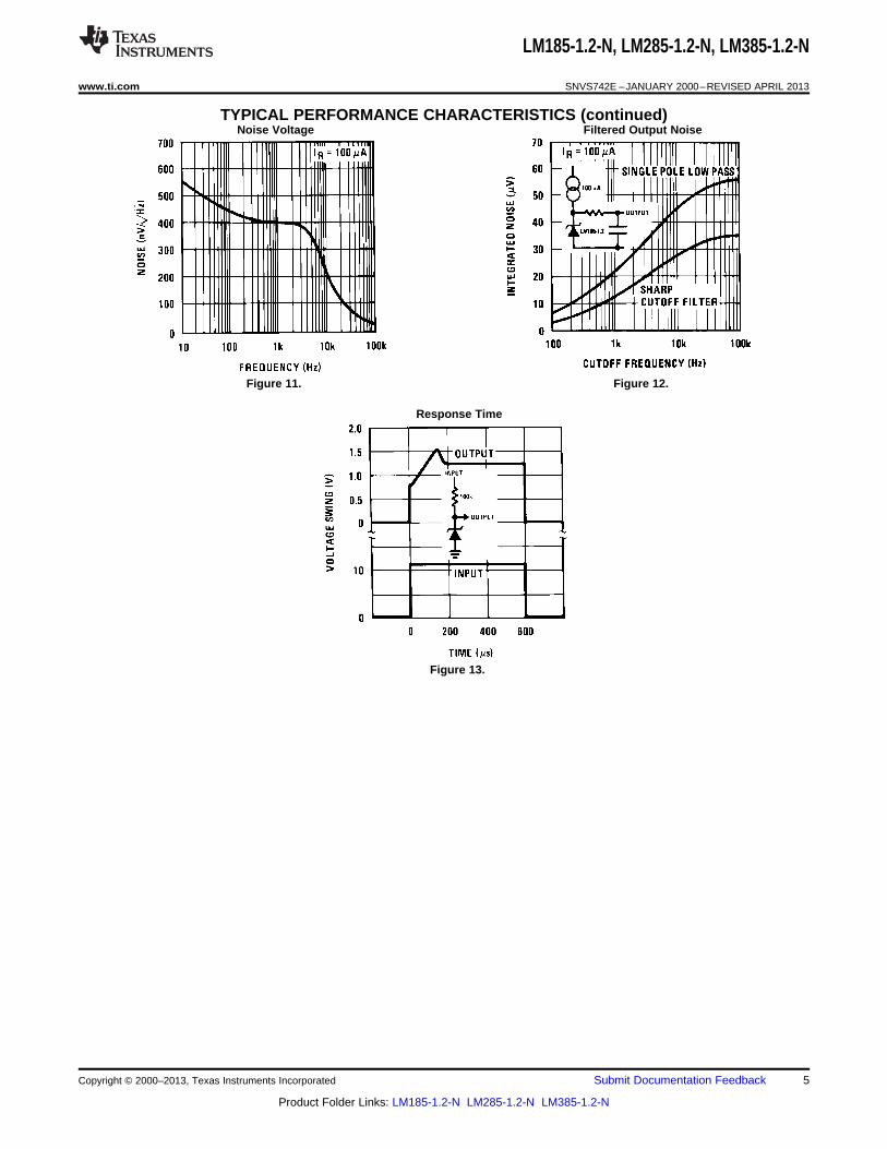
TYPICAL PERFORMANCE CHARACTERISTICS (continued)Noise Voltage Filtered Output Noise
Figure 11. Figure 12.
Response Time
Figure 13.
Copyright © 2000–2013, Texas Instruments Incorporated Submit Documentation Feedback 5
Product Folder Links: LM185-1.2-N LM285-1.2-N LM385-1.2-N

LM185-1.2-N, LM285-1.2-N, LM385-1.2-N
SNVS742E –JANUARY 2000–REVISED APRIL 2013 www.ti.com
TYPICAL APPLICATIONS
Figure 14. Wide Input Range Reference Figure 15. Micropower Reference from 9V Battery
Figure 16. Reference from 1.5V Battery
*IQ ≃ 30μA
Figure 17. Micropower* 5V Regulator
6 Submit Documentation Feedback Copyright © 2000–2013, Texas Instruments Incorporated
Product Folder Links: LM185-1.2-N LM285-1.2-N LM385-1.2-N

LM185-1.2-N, LM285-1.2-N, LM385-1.2-N
www.ti.com SNVS742E –JANUARY 2000–REVISED APRIL 2013
*IQ ≃20μA standby current
Figure 18. Micropower* 10V Reference
Figure 19. Figure 20. Precision 1μA to 1mA Current Sources
Copyright © 2000–2013, Texas Instruments Incorporated Submit Documentation Feedback 7
Product Folder Links: LM185-1.2-N LM285-1.2-N LM385-1.2-N

LM185-1.2-N, LM285-1.2-N, LM385-1.2-N
SNVS742E –JANUARY 2000–REVISED APRIL 2013 www.ti.com
METER THERMOMETERS
Calibration1. Short LM385-1.2-N, adjust R3 for IOUT= temp at 1μA/°K2. Remove short, adjust R2 for correct reading in centigrade†IQ at 1.3V≃500μAIQ at 1.6V≃2.4mA
Figure 21. 0°C−100°C Thermometer
Figure 22.
*2N3638 or 2N2907 select for inverse HFE ≃ 5†Select for operation at 1.3V‡IQ ≃ 600μA to 900μA
Figure 23. Lower Power Thermometer
8 Submit Documentation Feedback Copyright © 2000–2013, Texas Instruments Incorporated
Product Folder Links: LM185-1.2-N LM285-1.2-N LM385-1.2-N

LM185-1.2-N, LM285-1.2-N, LM385-1.2-N
www.ti.com SNVS742E –JANUARY 2000–REVISED APRIL 2013
Calibration1. Short LM385-1.2-N, adjust R3 for IOUT= temp at 1.8μA/°K2. Remove short, adjust R2 for correct reading in °F
Figure 24. 0°F−50°F Thermometer
Adjustment Procedure1. Adjust TC ADJ pot until voltage across R1 equals Kelvin temperature multiplied by the thermocouple Seebeckcoefficient.2. Adjust zero ADJ pot until voltage across R2 equals the thermocouple Seebeck coefficient multiplied by 273.2.
Figure 25. Micropower Thermocouple Cold Junction Compensator
Copyright © 2000–2013, Texas Instruments Incorporated Submit Documentation Feedback 9
Product Folder Links: LM185-1.2-N LM285-1.2-N LM385-1.2-N

LM185-1.2-N, LM285-1.2-N, LM385-1.2-N
SNVS742E –JANUARY 2000–REVISED APRIL 2013 www.ti.com
Thermocouple Seebeck R1 R2 Voltage Voltage
Type Coefficient (Ω) (Ω) Across R1 Across R2
(μV/°C) @ 25°C (mV)
(mV)
J 52.3 523 1.24k 15.60 14.32
T 42.8 432 1k 12.77 11.78
K 40.8 412 953Ω 12.17 11.17
S 6.4 63.4 150Ω 1.908 1.766
Typical supply current 50μA
Calibration1. Adjust R1 so that V1 = temp at 1mV/°K2. Adjust V2 to 273.2mV†IQ for 1.3V to 1.6V battery volt-age = 50μA to 150μA
Figure 26. Centigrade Thermometer
10 Submit Documentation Feedback Copyright © 2000–2013, Texas Instruments Incorporated
Product Folder Links: LM185-1.2-N LM285-1.2-N LM385-1.2-N

LM185-1.2-N, LM285-1.2-N, LM385-1.2-N
www.ti.com SNVS742E –JANUARY 2000–REVISED APRIL 2013
SCHEMATIC DIAGRAM
Copyright © 2000–2013, Texas Instruments Incorporated Submit Documentation Feedback 11
Product Folder Links: LM185-1.2-N LM285-1.2-N LM385-1.2-N
LM185-1.2-N, LM285-1.2-N, LM385-1.2-N
SNVS742E –JANUARY 2000–REVISED APRIL 2013 www.ti.com
REVISION HISTORY
Changes from Revision D (April 2013) to Revision E Page
• Changed layout of National Data Sheet to TI format .......................................................................................................... 11
12 Submit Documentation Feedback Copyright © 2000–2013, Texas Instruments Incorporated
Product Folder Links: LM185-1.2-N LM285-1.2-N LM385-1.2-N

PACKAGE OPTION ADDENDUM
www.ti.com 3-Oct-2018
Addendum-Page 1
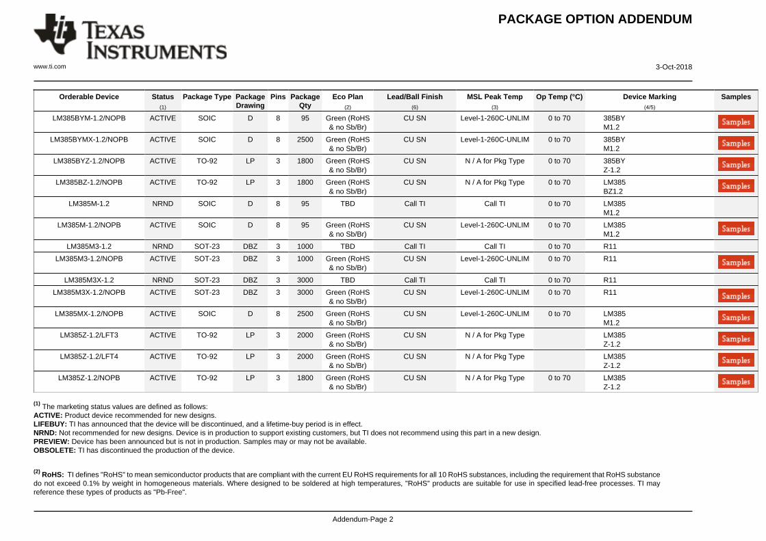
PACKAGING INFORMATION
Orderable Device Status(1)
Package Type PackageDrawing
Pins PackageQty
Eco Plan(2)
Lead/Ball Finish(6)
MSL Peak Temp(3)
Op Temp (°C) Device Marking(4/5)
Samples
LM185BYH-1.2/NOPB ACTIVE TO NDU 2 1000 Green (RoHS& no Sb/Br)
Call TI | POST-PLATE Level-1-NA-UNLIM -55 to 125 ( LM185BYH1.2, LM1 85BYH1.2)
LM185H-1.2/NOPB ACTIVE TO NDU 2 1000 Green (RoHS& no Sb/Br)
Call TI | POST-PLATE Level-1-NA-UNLIM -55 to 125 ( LM185H1.2, LM185 H1.2)
LM285BXM-1.2/NOPB ACTIVE SOIC D 8 95 Green (RoHS& no Sb/Br)
CU SN Level-1-260C-UNLIM -40 to 85 285BXM1.2
LM285BXMX-1.2/NOPB ACTIVE SOIC D 8 2500 Green (RoHS& no Sb/Br)
CU SN Level-1-260C-UNLIM -40 to 85 285BXM1.2
LM285BXZ-1.2/LFT4 ACTIVE TO-92 LP 3 2000 Green (RoHS& no Sb/Br)
CU SN N / A for Pkg Type 285BXZ-1.2
LM285BXZ-1.2/NOPB ACTIVE TO-92 LP 3 1800 Green (RoHS& no Sb/Br)
CU SN N / A for Pkg Type -40 to 85 285BXZ-1.2
LM285BYM-1.2/NOPB ACTIVE SOIC D 8 95 Green (RoHS& no Sb/Br)
CU SN Level-1-260C-UNLIM -40 to 85 285BYM1.2
LM285BYMX-1.2/NOPB ACTIVE SOIC D 8 2500 Green (RoHS& no Sb/Br)
CU SN Level-1-260C-UNLIM -40 to 85 285BYM1.2
LM285M-1.2/NOPB ACTIVE SOIC D 8 95 Green (RoHS& no Sb/Br)
CU SN Level-1-260C-UNLIM -40 to 85 LM285M1.2
LM285MX-1.2/NOPB ACTIVE SOIC D 8 2500 Green (RoHS& no Sb/Br)
CU SN Level-1-260C-UNLIM -40 to 85 LM285M1.2
LM285Z-1.2/NOPB ACTIVE TO-92 LP 3 1800 Green (RoHS& no Sb/Br)
CU SN N / A for Pkg Type -40 to 85 LM285Z-1.2
LM385BM-1.2/NOPB ACTIVE SOIC D 8 95 Green (RoHS& no Sb/Br)
CU SN Level-1-260C-UNLIM 0 to 70 LM385BM1.2
LM385BMX-1.2 NRND SOIC D 8 2500 TBD Call TI Call TI 0 to 70 LM385BM1.2
LM385BMX-1.2/NOPB ACTIVE SOIC D 8 2500 Green (RoHS& no Sb/Br)
CU SN Level-1-260C-UNLIM 0 to 70 LM385BM1.2
LM385BXM-1.2/NOPB ACTIVE SOIC D 8 95 Green (RoHS& no Sb/Br)
CU SN Level-1-260C-UNLIM 0 to 70 385BXM1.2
LM385BXMX-1.2/NOPB ACTIVE SOIC D 8 2500 Green (RoHS& no Sb/Br)
CU SN Level-1-260C-UNLIM 0 to 70 385BXM1.2
LM385BXZ-1.2/NOPB ACTIVE TO-92 LP 3 1800 Green (RoHS& no Sb/Br)
CU SN N / A for Pkg Type 0 to 70 385BXZ-1.2
PACKAGE OPTION ADDENDUM
www.ti.com 3-Oct-2018
Addendum-Page 2
Orderable Device Status(1)
Package Type PackageDrawing
Pins PackageQty
Eco Plan(2)
Lead/Ball Finish(6)
MSL Peak Temp(3)
Op Temp (°C) Device Marking(4/5)
Samples
LM385BYM-1.2/NOPB ACTIVE SOIC D 8 95 Green (RoHS& no Sb/Br)
CU SN Level-1-260C-UNLIM 0 to 70 385BYM1.2
LM385BYMX-1.2/NOPB ACTIVE SOIC D 8 2500 Green (RoHS& no Sb/Br)
CU SN Level-1-260C-UNLIM 0 to 70 385BYM1.2
LM385BYZ-1.2/NOPB ACTIVE TO-92 LP 3 1800 Green (RoHS& no Sb/Br)
CU SN N / A for Pkg Type 0 to 70 385BYZ-1.2
LM385BZ-1.2/NOPB ACTIVE TO-92 LP 3 1800 Green (RoHS& no Sb/Br)
CU SN N / A for Pkg Type 0 to 70 LM385BZ1.2
LM385M-1.2 NRND SOIC D 8 95 TBD Call TI Call TI 0 to 70 LM385M1.2
LM385M-1.2/NOPB ACTIVE SOIC D 8 95 Green (RoHS& no Sb/Br)
CU SN Level-1-260C-UNLIM 0 to 70 LM385M1.2
LM385M3-1.2 NRND SOT-23 DBZ 3 1000 TBD Call TI Call TI 0 to 70 R11
LM385M3-1.2/NOPB ACTIVE SOT-23 DBZ 3 1000 Green (RoHS& no Sb/Br)
CU SN Level-1-260C-UNLIM 0 to 70 R11
LM385M3X-1.2 NRND SOT-23 DBZ 3 3000 TBD Call TI Call TI 0 to 70 R11
LM385M3X-1.2/NOPB ACTIVE SOT-23 DBZ 3 3000 Green (RoHS& no Sb/Br)
CU SN Level-1-260C-UNLIM 0 to 70 R11
LM385MX-1.2/NOPB ACTIVE SOIC D 8 2500 Green (RoHS& no Sb/Br)
CU SN Level-1-260C-UNLIM 0 to 70 LM385M1.2
LM385Z-1.2/LFT3 ACTIVE TO-92 LP 3 2000 Green (RoHS& no Sb/Br)
CU SN N / A for Pkg Type LM385Z-1.2
LM385Z-1.2/LFT4 ACTIVE TO-92 LP 3 2000 Green (RoHS& no Sb/Br)
CU SN N / A for Pkg Type LM385Z-1.2
LM385Z-1.2/NOPB ACTIVE TO-92 LP 3 1800 Green (RoHS& no Sb/Br)
CU SN N / A for Pkg Type 0 to 70 LM385Z-1.2
(1) The marketing status values are defined as follows:ACTIVE: Product device recommended for new designs.LIFEBUY: TI has announced that the device will be discontinued, and a lifetime-buy period is in effect.NRND: Not recommended for new designs. Device is in production to support existing customers, but TI does not recommend using this part in a new design.PREVIEW: Device has been announced but is not in production. Samples may or may not be available.OBSOLETE: TI has discontinued the production of the device.
(2) RoHS: TI defines "RoHS" to mean semiconductor products that are compliant with the current EU RoHS requirements for all 10 RoHS substances, including the requirement that RoHS substancedo not exceed 0.1% by weight in homogeneous materials. Where designed to be soldered at high temperatures, "RoHS" products are suitable for use in specified lead-free processes. TI mayreference these types of products as "Pb-Free".

PACKAGE OPTION ADDENDUM
www.ti.com 3-Oct-2018
Addendum-Page 3
RoHS Exempt: TI defines "RoHS Exempt" to mean products that contain lead but are compliant with EU RoHS pursuant to a specific EU RoHS exemption.Green: TI defines "Green" to mean the content of Chlorine (Cl) and Bromine (Br) based flame retardants meet JS709B low halogen requirements of <=1000ppm threshold. Antimony trioxide basedflame retardants must also meet the <=1000ppm threshold requirement.
(3) MSL, Peak Temp. - The Moisture Sensitivity Level rating according to the JEDEC industry standard classifications, and peak solder temperature.
(4) There may be additional marking, which relates to the logo, the lot trace code information, or the environmental category on the device.
(5) Multiple Device Markings will be inside parentheses. Only one Device Marking contained in parentheses and separated by a "~" will appear on a device. If a line is indented then it is a continuationof the previous line and the two combined represent the entire Device Marking for that device.
(6) Lead/Ball Finish - Orderable Devices may have multiple material finish options. Finish options are separated by a vertical ruled line. Lead/Ball Finish values may wrap to two lines if the finishvalue exceeds the maximum column width.
Important Information and Disclaimer:The information provided on this page represents TI's knowledge and belief as of the date that it is provided. TI bases its knowledge and belief on informationprovided by third parties, and makes no representation or warranty as to the accuracy of such information. Efforts are underway to better integrate information from third parties. TI has taken andcontinues to take reasonable steps to provide representative and accurate information but may not have conducted destructive testing or chemical analysis on incoming materials and chemicals.TI and TI suppliers consider certain information to be proprietary, and thus CAS numbers and other limited information may not be available for release.
In no event shall TI's liability arising out of such information exceed the total purchase price of the TI part(s) at issue in this document sold by TI to Customer on an annual basis.

TAPE AND REEL INFORMATION
*All dimensions are nominal
Device PackageType
PackageDrawing
Pins SPQ ReelDiameter
(mm)
ReelWidth
W1 (mm)
A0(mm)
B0(mm)
K0(mm)
P1(mm)
W(mm)
Pin1Quadrant
LM285BXMX-1.2/NOPB SOIC D 8 2500 330.0 12.4 6.5 5.4 2.0 8.0 12.0 Q1
LM285BYMX-1.2/NOPB SOIC D 8 2500 330.0 12.4 6.5 5.4 2.0 8.0 12.0 Q1
LM285MX-1.2/NOPB SOIC D 8 2500 330.0 12.4 6.5 5.4 2.0 8.0 12.0 Q1
LM385BMX-1.2 SOIC D 8 2500 330.0 12.4 6.5 5.4 2.0 8.0 12.0 Q1
LM385BMX-1.2/NOPB SOIC D 8 2500 330.0 12.4 6.5 5.4 2.0 8.0 12.0 Q1
LM385BXMX-1.2/NOPB SOIC D 8 2500 330.0 12.4 6.5 5.4 2.0 8.0 12.0 Q1
LM385BYMX-1.2/NOPB SOIC D 8 2500 330.0 12.4 6.5 5.4 2.0 8.0 12.0 Q1
LM385M3-1.2 SOT-23 DBZ 3 1000 178.0 8.4 3.3 2.9 1.22 4.0 8.0 Q3
LM385M3-1.2/NOPB SOT-23 DBZ 3 1000 178.0 8.4 3.3 2.9 1.22 4.0 8.0 Q3
LM385M3X-1.2 SOT-23 DBZ 3 3000 178.0 8.4 3.3 2.9 1.22 4.0 8.0 Q3
LM385M3X-1.2/NOPB SOT-23 DBZ 3 3000 178.0 8.4 3.3 2.9 1.22 4.0 8.0 Q3
LM385MX-1.2/NOPB SOIC D 8 2500 330.0 12.4 6.5 5.4 2.0 8.0 12.0 Q1
PACKAGE MATERIALS INFORMATION
www.ti.com 5-Dec-2014
Pack Materials-Page 1

*All dimensions are nominal
Device Package Type Package Drawing Pins SPQ Length (mm) Width (mm) Height (mm)
LM285BXMX-1.2/NOPB SOIC D 8 2500 367.0 367.0 35.0
LM285BYMX-1.2/NOPB SOIC D 8 2500 367.0 367.0 35.0
LM285MX-1.2/NOPB SOIC D 8 2500 367.0 367.0 35.0
LM385BMX-1.2 SOIC D 8 2500 367.0 367.0 35.0
LM385BMX-1.2/NOPB SOIC D 8 2500 367.0 367.0 35.0
LM385BXMX-1.2/NOPB SOIC D 8 2500 367.0 367.0 35.0
LM385BYMX-1.2/NOPB SOIC D 8 2500 367.0 367.0 35.0
LM385M3-1.2 SOT-23 DBZ 3 1000 210.0 185.0 35.0
LM385M3-1.2/NOPB SOT-23 DBZ 3 1000 210.0 185.0 35.0
LM385M3X-1.2 SOT-23 DBZ 3 3000 210.0 185.0 35.0
LM385M3X-1.2/NOPB SOT-23 DBZ 3 3000 210.0 185.0 35.0
LM385MX-1.2/NOPB SOIC D 8 2500 367.0 367.0 35.0
PACKAGE MATERIALS INFORMATION
www.ti.com 5-Dec-2014
Pack Materials-Page 2


www.ti.com
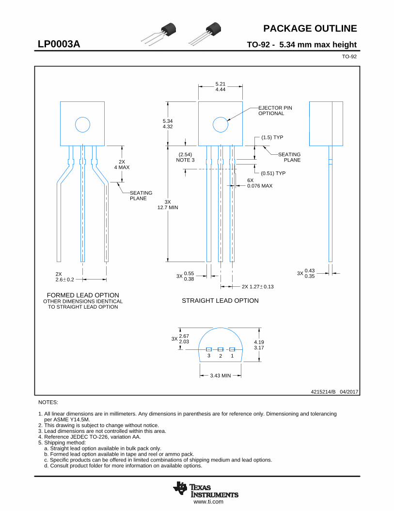
PACKAGE OUTLINE
3X 2.672.03
5.214.44
5.344.32
3X12.7 MIN
2X 1.27 0.13
3X 0.550.38
4.193.17
3.43 MIN
3X 0.430.35
(2.54)NOTE 3
2X2.6 0.2
2X4 MAX
SEATINGPLANE
6X0.076 MAX
(0.51) TYP
(1.5) TYP
TO-92 - 5.34 mm max heightLP0003ATO-92
4215214/B 04/2017
NOTES: 1. All linear dimensions are in millimeters. Any dimensions in parenthesis are for reference only. Dimensioning and tolerancing per ASME Y14.5M.2. This drawing is subject to change without notice.3. Lead dimensions are not controlled within this area.4. Reference JEDEC TO-226, variation AA.5. Shipping method: a. Straight lead option available in bulk pack only. b. Formed lead option available in tape and reel or ammo pack. c. Specific products can be offered in limited combinations of shipping medium and lead options. d. Consult product folder for more information on available options.
EJECTOR PINOPTIONAL
PLANESEATING
STRAIGHT LEAD OPTION
3 2 1
SCALE 1.200
FORMED LEAD OPTIONOTHER DIMENSIONS IDENTICAL
TO STRAIGHT LEAD OPTION
SCALE 1.200

www.ti.com
EXAMPLE BOARD LAYOUT
0.05 MAXALL AROUND
TYP
(1.07)
(1.5) 2X (1.5)
2X (1.07)(1.27)
(2.54)
FULL RTYP
( 1.4)0.05 MAXALL AROUND
TYP
(2.6)
(5.2)
(R0.05) TYP
3X ( 0.9) HOLE
2X ( 1.4)METAL
3X ( 0.85) HOLE
(R0.05) TYP
4215214/B 04/2017
TO-92 - 5.34 mm max heightLP0003ATO-92
LAND PATTERN EXAMPLEFORMED LEAD OPTIONNON-SOLDER MASK DEFINED
SCALE:15X
SOLDER MASKOPENING
METAL
2XSOLDER MASKOPENING
1 2 3
LAND PATTERN EXAMPLESTRAIGHT LEAD OPTIONNON-SOLDER MASK DEFINED
SCALE:15X
METALTYP
SOLDER MASKOPENING
2XSOLDER MASKOPENING
2XMETAL
1 2 3

www.ti.com
TAPE SPECIFICATIONS
19.017.5
13.711.7
11.08.5
0.5 MIN
TYP-4.33.7
9.758.50
TYP2.92.4
6.755.95
13.012.4
(2.5) TYP
16.515.5
3223
4215214/B 04/2017
TO-92 - 5.34 mm max heightLP0003ATO-92
FOR FORMED LEAD OPTION PACKAGE

MECHANICAL DATA
NDU0002A
www.ti.com
H02A (Rev F)

4203227/C

www.ti.com
PACKAGE OUTLINE
C
TYP0.200.08
0.25
2.642.10
1.12 MAX
TYP0.100.01
3X 0.50.3
TYP0.60.2
1.9
0.95
TYP-80
A
3.042.80
B1.41.2
(0.95)
SOT-23 - 1.12 mm max heightDBZ0003ASMALL OUTLINE TRANSISTOR
4214838/C 04/2017
NOTES: 1. All linear dimensions are in millimeters. Any dimensions in parenthesis are for reference only. Dimensioning and tolerancing per ASME Y14.5M.2. This drawing is subject to change without notice.3. Reference JEDEC registration TO-236, except minimum foot length.
0.2 C A B
1
3
2
INDEX AREAPIN 1
GAGE PLANE
SEATING PLANE
0.1 C
SCALE 4.000

www.ti.com
EXAMPLE BOARD LAYOUT
0.07 MAXALL AROUND
0.07 MINALL AROUND
3X (1.3)
3X (0.6)
(2.1)
2X (0.95)
(R0.05) TYP
4214838/C 04/2017
SOT-23 - 1.12 mm max heightDBZ0003ASMALL OUTLINE TRANSISTOR
NOTES: (continued) 4. Publication IPC-7351 may have alternate designs. 5. Solder mask tolerances between and around signal pads can vary based on board fabrication site.
SYMM
LAND PATTERN EXAMPLESCALE:15X
PKG
1
3
2
SOLDER MASKOPENINGMETAL UNDER
SOLDER MASK
SOLDER MASKDEFINED
METALSOLDER MASKOPENING
NON SOLDER MASKDEFINED
(PREFERRED)
SOLDER MASK DETAILS

www.ti.com
EXAMPLE STENCIL DESIGN
(2.1)
2X(0.95)
3X (1.3)
3X (0.6)
(R0.05) TYP
SOT-23 - 1.12 mm max heightDBZ0003ASMALL OUTLINE TRANSISTOR
4214838/C 04/2017
NOTES: (continued) 6. Laser cutting apertures with trapezoidal walls and rounded corners may offer better paste release. IPC-7525 may have alternate design recommendations. 7. Board assembly site may have different recommendations for stencil design.
SOLDER PASTE EXAMPLEBASED ON 0.125 THICK STENCIL
SCALE:15X
SYMM
PKG
1
3
2

IMPORTANT NOTICE AND DISCLAIMER
TI PROVIDES TECHNICAL AND RELIABILITY DATA (INCLUDING DATASHEETS), DESIGN RESOURCES (INCLUDING REFERENCEDESIGNS), APPLICATION OR OTHER DESIGN ADVICE, WEB TOOLS, SAFETY INFORMATION, AND OTHER RESOURCES “AS IS”AND WITH ALL FAULTS, AND DISCLAIMS ALL WARRANTIES, EXPRESS AND IMPLIED, INCLUDING WITHOUT LIMITATION ANYIMPLIED WARRANTIES OF MERCHANTABILITY, FITNESS FOR A PARTICULAR PURPOSE OR NON-INFRINGEMENT OF THIRDPARTY INTELLECTUAL PROPERTY RIGHTS.These resources are intended for skilled developers designing with TI products. You are solely responsible for (1) selecting the appropriateTI products for your application, (2) designing, validating and testing your application, and (3) ensuring your application meets applicablestandards, and any other safety, security, or other requirements. These resources are subject to change without notice. TI grants youpermission to use these resources only for development of an application that uses the TI products described in the resource. Otherreproduction and display of these resources is prohibited. No license is granted to any other TI intellectual property right or to any thirdparty intellectual property right. TI disclaims responsibility for, and you will fully indemnify TI and its representatives against, any claims,damages, costs, losses, and liabilities arising out of your use of these resources.TI’s products are provided subject to TI’s Terms of Sale (www.ti.com/legal/termsofsale.html) or other applicable terms available either onti.com or provided in conjunction with such TI products. TI’s provision of these resources does not expand or otherwise alter TI’s applicablewarranties or warranty disclaimers for TI products.
Mailing Address: Texas Instruments, Post Office Box 655303, Dallas, Texas 75265Copyright © 2018, Texas Instruments Incorporated