Embed Size (px)
Citation preview

SONiX Technology Co., Ltd.
SN8F5708 Series Datasheet
8051-based Microcontroller
SN8F5705 SN8F5707 SN8F5708 SN8F570870 SN8F570812 SN8F57082 SN8F570822 SN8F57084 SN8F57085 SN8F57086 SN8F57087
www.sonix.com.tw SN8F5708 Series
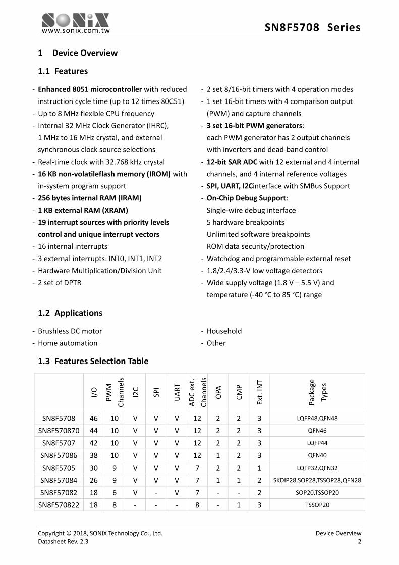
1 Device Overview
1.1 Features
- Enhanced 8051 microcontroller with reduced instruction cycle time (up to 12 times 80C51)
- Up to 8 MHz flexible CPU frequency - Internal 32 MHz Clock Generator (IHRC),
1 MHz to 16 MHz crystal, and external synchronous clock source selections
- Real-time clock with 32.768 kHz crystal - 16 KB non-volatileflash memory (IROM) with
in-system program support - 256 bytes internal RAM (IRAM) - 1 KB external RAM (XRAM) - 19 interrupt sources with priority levels
control and unique interrupt vectors - 16 internal interrupts - 3 external interrupts: INT0, INT1, INT2 - Hardware Multiplication/Division Unit - 2 set of DPTR
- 2 set 8/16-bit timers with 4 operation modes - 1 set 16-bit timers with 4 comparison output
(PWM) and capture channels - 3 set 16-bit PWM generators:
each PWM generator has 2 output channels with inverters and dead-band control
- 12-bit SAR ADC with 12 external and 4 internal channels, and 4 internal reference voltages
- SPI, UART, I2Cinterface with SMBus Support - On-Chip Debug Support:
Single-wire debug interface 5 hardware breakpoints Unlimited software breakpoints ROM data security/protection
- Watchdog and programmable external reset - 1.8/2.4/3.3-V low voltage detectors - Wide supply voltage (1.8 V – 5.5 V) and
temperature (-40 °C to 85 °C) range
1.2 Applications
- Brushless DC motor - Home automation
- Household - Other
1.3 Features Selection Table
I/O
PWM
Ch
anne
ls
I2C
SPI
UART
ADC
ext.
Chan
nels
OPA
CMP
Ext.
INT
Pack
age
Type
s
SN8F5708 46 10 V V V 12 2 2 3 LQFP48,QFN48
SN8F570870 44 10 V V V 12 2 2 3 QFN46
SN8F5707 42 10 V V V 12 2 2 3 LQFP44
SN8F57086 38 10 V V V 12 1 2 3 QFN40
SN8F5705 30 9 V V V 7 2 2 1 LQFP32,QFN32
SN8F57084 26 9 V V V 7 1 1 2 SKDIP28,SOP28,TSSOP28,QFN28
SN8F57082 18 6 V - V 7 - - 2 SOP20,TSSOP20
SN8F570822 18 8 - - - 8 - 1 3 TSSOP20
Copyright © 2018, SONiX Technology Co., Ltd. Device Overview Datasheet Rev. 2.3 2
www.sonix.com.tw SN8F5708 Series
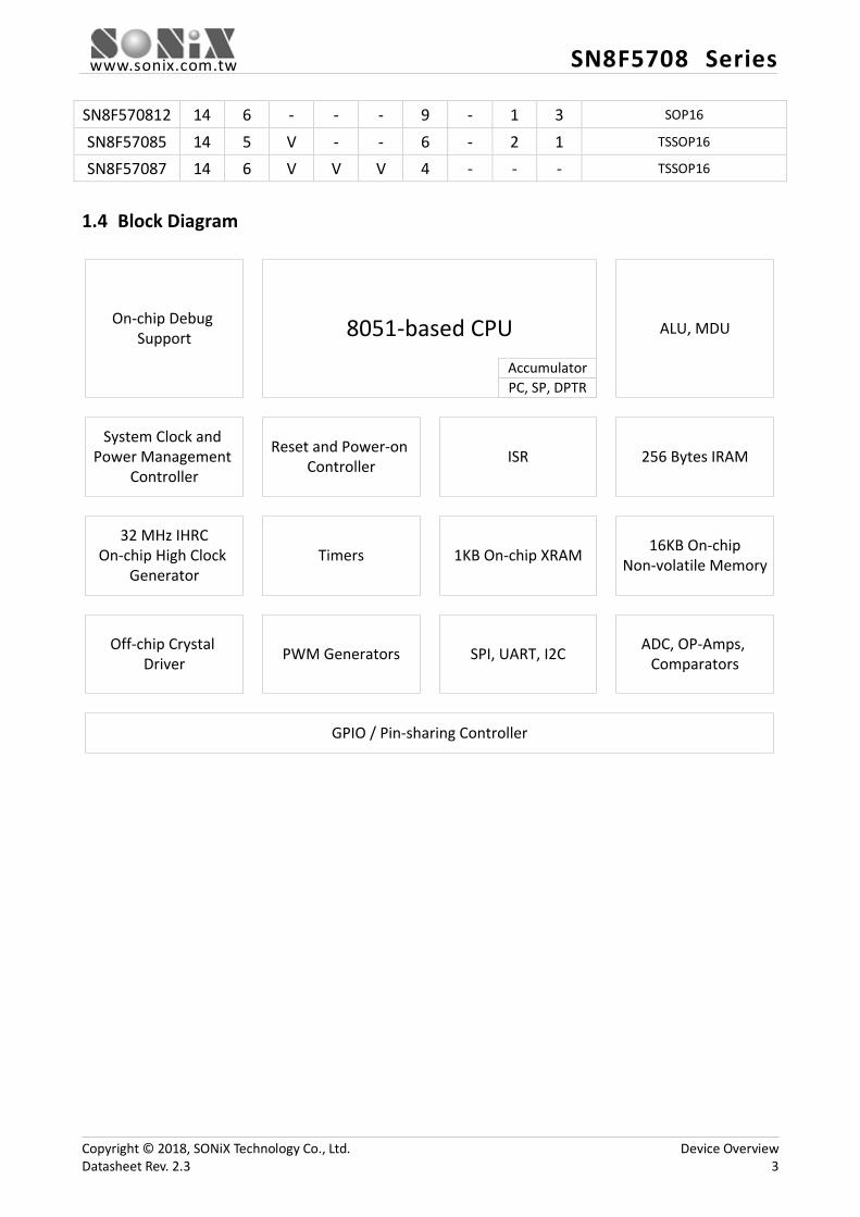
SN8F570812 14 6 - - - 9 - 1 3 SOP16
SN8F57085 14 5 V - - 6 - 2 1 TSSOP16
SN8F57087 14 6 V V V 4 - - - TSSOP16
1.4 Block Diagram
8051-based CPU
ISR
ALU, MDU
256 Bytes IRAMReset and Power-on Controller
1KB On-chip XRAM 16KB On-chipNon-volatile Memory
ADC, OP-Amps, ComparatorsSPI, UART, I2C
GPIO / Pin-sharing Controller
Timers
PWM Generators
System Clock and Power Management
Controller
32 MHz IHRCOn-chip High Clock
Generator
Off-chip Crystal Driver
On-chip Debug Support
PC, SP, DPTRAccumulator
Copyright © 2018, SONiX Technology Co., Ltd. Device Overview Datasheet Rev. 2.3 3
www.sonix.com.tw SN8F5708 Series
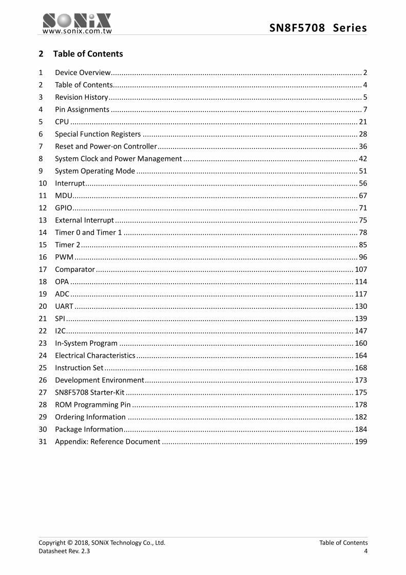
2 Table of Contents
1 Device Overview ...................................................................................................................... 2 2 Table of Contents..................................................................................................................... 4 3 Revision History ....................................................................................................................... 5 4 Pin Assignments ...................................................................................................................... 7 5 CPU ....................................................................................................................................... 21 6 Special Function Registers ..................................................................................................... 28 7 Reset and Power-on Controller .............................................................................................. 36 8 System Clock and Power Management .................................................................................. 42 9 System Operating Mode ........................................................................................................ 51 10 Interrupt ................................................................................................................................ 56 11 MDU...................................................................................................................................... 67 12 GPIO ...................................................................................................................................... 71 13 External Interrupt .................................................................................................................. 75 14 Timer 0 and Timer 1 .............................................................................................................. 78 15 Timer 2 .................................................................................................................................. 85 16 PWM ..................................................................................................................................... 96 17 Comparator ......................................................................................................................... 107 18 OPA ..................................................................................................................................... 114 19 ADC ..................................................................................................................................... 117 20 UART ................................................................................................................................... 130 21 SPI ....................................................................................................................................... 139 22 I2C ....................................................................................................................................... 147 23 In-System Program .............................................................................................................. 160 24 Electrical Characteristics ...................................................................................................... 164 25 Instruction Set ..................................................................................................................... 168 26 Development Environment .................................................................................................. 173 27 SN8F5708 Starter-Kit ........................................................................................................... 175 28 ROM Programming Pin ........................................................................................................ 178 29 Ordering Information .......................................................................................................... 182 30 Package Information ............................................................................................................ 184 31 Appendix: Reference Document .......................................................................................... 199
Copyright © 2018, SONiX Technology Co., Ltd. Table of Contents Datasheet Rev. 2.3 4
www.sonix.com.tw SN8F5708 Series
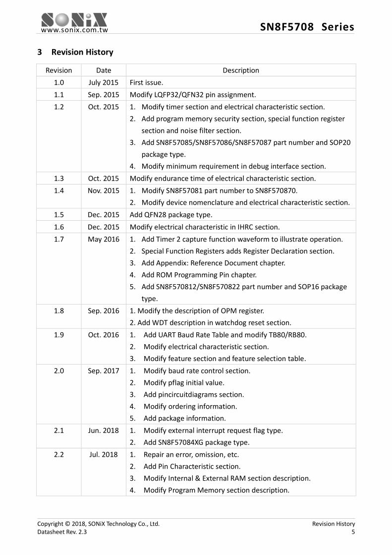
3 Revision History
Revision Date Description 1.0 July 2015 First issue. 1.1 Sep. 2015 Modify LQFP32/QFN32 pin assignment. 1.2 Oct. 2015 1. Modify timer section and electrical characteristic section.
2. Add program memory security section, special function register section and noise filter section.
3. Add SN8F57085/SN8F57086/SN8F57087 part number and SOP20 package type.
4. Modify minimum requirement in debug interface section. 1.3 Oct. 2015 Modify endurance time of electrical characteristic section. 1.4 Nov. 2015 1. Modify SN8F57081 part number to SN8F570870.
2. Modify device nomenclature and electrical characteristic section. 1.5 Dec. 2015 Add QFN28 package type. 1.6 Dec. 2015 Modify electrical characteristic in IHRC section. 1.7 May 2016 1. Add Timer 2 capture function waveform to illustrate operation.
2. Special Function Registers adds Register Declaration section. 3. Add Appendix: Reference Document chapter. 4. Add ROM Programming Pin chapter. 5. Add SN8F570812/SN8F570822 part number and SOP16 package
type. 1.8 Sep. 2016 1. Modify the description of OPM register.
2. Add WDT description in watchdog reset section. 1.9 Oct. 2016 1. Add UART Baud Rate Table and modify TB80/RB80.
2. Modify electrical characteristic section. 3. Modify feature section and feature selection table.
2.0 Sep. 2017 1. Modify baud rate control section. 2. Modify pflag initial value. 3. Add pincircuitdiagrams section. 4. Modify ordering information. 5. Add package information.
2.1 Jun. 2018 1. Modify external interrupt request flag type. 2. Add SN8F57084XG package type.
2.2 Jul. 2018 1. Repair an error, omission, etc. 2. Add Pin Characteristic section. 3. Modify Internal & External RAM section description. 4. Modify Program Memory section description.
Copyright © 2018, SONiX Technology Co., Ltd. Revision History Datasheet Rev. 2.3 5
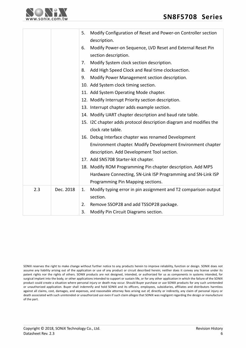
www.sonix.com.tw SN8F5708 Series
5. Modify Configuration of Reset and Power-on Controller section description.
6. Modify Power-on Sequence, LVD Reset and External Reset Pin section description.
7. Modify System clock section description. 8. Add High Speed Clock and Real time clocksection. 9. Modify Power Management section description. 10. Add System clock timing section. 11. Add System Operating Mode chapter. 12. Modify Interrupt Priority section description. 13. Interrupt chapter adds example section. 14. Modify UART chapter description and baud rate table. 15. I2C chapter adds protocol description diagram and modifies the
clock rate table. 16. Debug Interface chapter was renamed Development
Environment chapter. Modify Development Environment chapter description. Add Development Tool section.
17. Add SN5708 Starter-kit chapter. 18. Modify ROM Programming Pin chapter description. Add MP5
Hardware Connecting, SN-Link ISP Programming and SN-Link ISP Programming Pin Mapping sections.
2.3 Dec. 2018 1. Modify typing error in pin assignment and T2 comparison output section.
2. Remove SSOP28 and add TSSOP28 package. 3. Modify Pin Circuit Diagrams section.
SONIX reserves the right to make change without further notice to any products herein to improve reliability, function or design. SONIX does not assume any liability arising out of the application or use of any product or circuit described herein; neither does it convey any license under its patent rights nor the rights of others. SONIX products are not designed, intended, or authorized for us as components in systems intended, for surgical implant into the body, or other applications intended to support or sustain life, or for any other application in which the failure of the SONIX product could create a situation where personal injury or death may occur. Should Buyer purchase or use SONIX products for any such unintended or unauthorized application. Buyer shall indemnify and hold SONIX and its officers, employees, subsidiaries, affiliates and distributors harmless against all claims, cost, damages, and expenses, and reasonable attorney fees arising out of, directly or indirectly, any claim of personal injury or death associated with such unintended or unauthorized use even if such claim alleges that SONIX was negligent regarding the design or manufacture of the part.
Copyright © 2018, SONiX Technology Co., Ltd. Revision History Datasheet Rev. 2.3 6
www.sonix.com.tw SN8F5708 Series
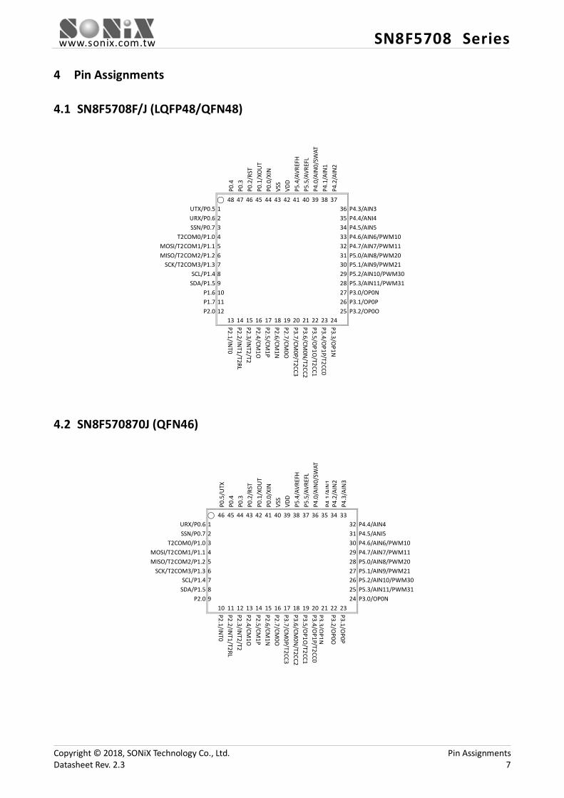
4 Pin Assignments
4.1 SN8F5708F/J (LQFP48/QFN48)
P0.4
P0
.3
P0.2
/RST
P0
.1/X
OU
T P0
.0/X
IN
VSS
VDD
P5.4
/AVR
EFH
P5
.5/A
VREF
L P4
.0/A
IN0/
SWAT
P4
.1/A
IN1
P4.2
/AIN
2
⃝ 48 47 46 45 44 43 42 41 40 39 38 37 UTX/P0.5 1 36 P4.3/AIN3 URX/P0.6 2 35 P4.4/ANI4 SSN/P0.7 3 34 P4.5/AIN5
T2COM0/P1.0 4 33 P4.6/AIN6/PWM10 MOSI/T2COM1/P1.1 5 32 P4.7/AIN7/PWM11 MISO/T2COM2/P1.2 6 31 P5.0/AIN8/PWM20
SCK/T2COM3/P1.3 7 30 P5.1/AIN9/PWM21 SCL/P1.4 8 29 P5.2/AIN10/PWM30
SDA/P1.5 9 28 P5.3/AIN11/PWM31 P1.6 10 27 P3.0/OP0N P1.7 11 26 P3.1/OP0P P2.0 12 25 P3.2/OP0O
13 14 15 16 17 18 19 20 21 22 23 24
P2.1/INT0
P2.2/INT1/T2RL
P2.3/INT2/T2
P2.4/CM1O
P2.5/CM
1P P2.6/CM
1N
P2.7/CM0O
P3.7/CM
0P/T2CC3 P3.6/CM
0N/T2CC2
P3.5/OP1O
/T2CC1 P3.4/O
P1P/T2CC0 P3.3/O
P1N
4.2 SN8F570870J (QFN46)
P0.5
/UTX
P0
.4
P0.3
P0
.2/R
ST
P0.1
/XO
UT
P0.0
/XIN
VS
S VD
D P5
.4/A
VREF
H
P5.5
/AVR
EFL
P4.0
/AIN
0/SW
AT
P4.1
/AIN
1 P4
.2/A
IN2
P4.3
/AIN
3
⃝ 46 45 44 43 42 41 40 39 38 37 36 35 34 33 URX/P0.6 1 32 P4.4/AIN4 SSN/P0.7 2 31 P4.5/ANI5
T2COM0/P1.0 3 30 P4.6/AIN6/PWM10 MOSI/T2COM1/P1.1 4 29 P4.7/AIN7/PWM11 MISO/T2COM2/P1.2 5 28 P5.0/AIN8/PWM20
SCK/T2COM3/P1.3 6 27 P5.1/AIN9/PWM21 SCL/P1.4 7 26 P5.2/AIN10/PWM30
SDA/P1.5 8 25 P5.3/AIN11/PWM31 P2.0 9 24 P3.0/OP0N
10 11 12 13 14 15 16 17 18 19 20 21 22 23
P2.1/INT0
P2.2/INT1/T2RL
P2.3/INT2/T2
P2.4/CM1O
P2.5/CM
1P P2.6/CM
1N
P2.7/CM0O
P3.7/CM
0P/T2CC3 P3.6/CM
0N/T2CC2
P3.5/OP1O
/T2CC1 P3.4/O
P1P/T2CC0 P3.3/O
P1N
P3.2/OP0O
P3.1/O
P0P
Copyright © 2018, SONiX Technology Co., Ltd. Pin Assignments Datasheet Rev. 2.3 7

www.sonix.com.tw SN8F5708 Series
4.3 SN8F5707F (LQFP44)
P0.5
/UTX
P0
.2/R
ST
P0.1
/XO
UT
P0.0
/XIN
VS
S VD
D P5
.4/A
VREF
H
P5.5
/AVR
EFL
P4.0
/AIN
0/SW
AT
P4.1
/AIN
1 P4
.2/A
IN2
⃝ 44 43 42 41 40 39 38 37 36 35 34 URX/P0.6 1 33 P4.3/AIN3 SSN/P0.7 2 32 P4.4/AIN4
T2COM0/P1.0 3 31 P4.5/AIN5 MOSI/T2COM1/P1.1 4 30 P4.6/AIN6/PWM10 MISO/T2COM2/P1.2 5 29 P4.7/AIN7/PWM11
SCK/T2COM3/P1.3 6 28 P5.0/AIN8/PWM20 SCL/P1.4 7 27 P5.1/AIN9/PWM21
SDA/P1.5 8 26 P5.2/AIN10/PWM30 P2.0 9 25 P5.3/AIN11/PWM31
INT0/P2.1 10 24 P3.0/OP0N T2RL/INT1/P2.2 11 23 P3.1/OP0P
12 13 14 15 16 17 18 19 20 21 22
P2.3/INT2/T2
P2.4/CM1O
P2.5/CM
1P P2.6/CM
1N
P2.7/CM0O
P3.7/CM
0P/T2CC3 P3.6/CM
0N/T2CC2
P3.5/OP1O
/T2CC1 P3.4/O
P1P/T2CC0 P3.3/O
P1N
P3.2/OP0O
4.4 SN8F57086J (QFN40)
P0.5
/UTX
P0
.2/R
ST
P0.1
/XO
UT
P0.0
/XIN
VS
S VD
D P5
.4/A
VREF
H
P5.5
/AVR
EFL
P4.0
/AIN
0/SW
AT
P4.1
/AIN
1
⃝ 40 39 38 37 36 35 34 33 32 31 URX/P0.6 1 30 P4.2/AIN2 SSN/P0.7 2 29 P4.3/AIN3
T2COM0/P1.0 3 28 P4.4/AIN4 MOSI/T2COM1/P1.1 4 27 P4.5/AIN5 MISO/T2COM2/P1.2 5 26 P4.6/AIN6/PWM10
SCK/T2COM3/P1.3 6 25 P4.7/AIN7/PWM11 SCL/P1.4 7 24 P5.0/AIN8/PWM20
SDA/P1.5 8 23 P5.1/AIN9/PWM21 INT0/P2.1 9 22 P5.2/AIN10/PWM30
T2RL/INT1/P2.2 10 21 P5.3/AIN11/PWM31 11 12 13 14 15 16 17 18 19 20
P2.3/INT2/T2
P2.6/CM1N
P2.7/CM
0O
P3.7/CM0P/T2CC3
P3.6/CM0N
/T2CC2 P3.5/O
P1O/T2CC1
P3.4/OP1P/T2CC0
P3.3/OP1N
P3.1/O
P0P P3.0/O
P0N
Copyright © 2018, SONiX Technology Co., Ltd. Pin Assignments Datasheet Rev. 2.3 8

www.sonix.com.tw SN8F5708 Series
4.5 SN8F5705F/J (LQFP32/QFN32)
RST/
P0.2
P0
.1/X
OU
T P0
.0/X
IN
VSS
VDD
P5.4
/AVR
EFH
P5
.5/A
VREF
L P4
.0/A
IN0/
SWAT
⃝ 32 31 30 29 28 27 26 25 UTX/P0.5 1 24 P4.6/AIN6/PWM10 URX/P0.6 2 23 P4.7/AIN7/PWM11 SSN/P0.7 3 22 P5.0/AIN8/PWM20
MOSI/T2COM1/P1.1 4 21 P5.1/AIN9/PWM21 MISO/T2COM2/P1.2 5 20 P5.2/AIN10/PWM30
SCK/T2COM3/P1.3 6 19 P5.3/AIN11/PWM31 SCL/P1.4 7 18 P3.0/OP0N
SDA/P1.5 8 17 P3.1/OP0P 9 10 11 12 13 14 15 16
P2.2/INT1/T2RL
P2.6/CM1N
P2.7/CM
0O
P3.6/CM0N
/T2CC2 P3.5/O
P1O/T2CC1
P3.4/OP1P/T2CC0
P3.3/OP1N
P3.2/O
P0O
4.6 SN8F57084K/S/X (SKDIP28/SOP28/TSSOP28)
VSS 1 U 28 VDD XIN/P0.0 2 27 P5.4/AVREFH
XOUT/P0.1 3 26 P5.5/AVREFL RST/P0.2 4 25 P4.0/AIN0/SWAT UTX/P0.5 5 24 P4.6/AIN6/PWM10 URX/P0.6 6 23 P4.7/AIN7/PWM11 SSN/P0.7 7 22 P5.0/AIN8/PWM20
MOSI/T2COM1/P1.1 8 21 P5.1/AIN9/PWM21 MISO/T2COM2/P1.2 9 20 P5.2/AIN10/PWM30
SCK/T2COM3/P1.3 10 19 P5.3/AIN11/PWM31 SCL/P1.4 11 18 P3.3/OP1N
SDA/P1.5 12 17 P3.4/OP1P/T2CC0 T2RL/INT1/P2.2 13 16 P3.5/OP1O/T2CC1
T2/INT2/P2.3 14 15 P2.6/CM1N
Copyright © 2018, SONiX Technology Co., Ltd. Pin Assignments Datasheet Rev. 2.3 9

www.sonix.com.tw SN8F5708 Series
4.7 SN8F57084J (QFN28)
P0.2
/RST
P0
.1/X
OU
T P0
.0/X
IN
VSS
VDD
P5.4
/AVR
EFH
P5
.5/A
VREF
L
⃝ 28 27 26 25 24 23 22 UTX/P0.5 1 21 P4.0/AIN0/SWAT URX/P0.6 2 20 P4.6/AIN6/PWM10 SSN/P0.7 3 19 P4.7/AIN7/PWM11
MOSI/T2COM1/P1.1 4 18 P5.0/AIN8/PWM20 MISO/T2COM2/P1.2 5 17 P5.1/AIN9/PWM21
SCK/T2COM3/P1.3 6 16 P5.2/AIN10/PWM30 SCL/P1.4 7 15 P5.3/AIN11/PWM31
8 9 10 11 12 13 14
P1.5/SDA P2.2/IN
T1/T2RL P2.3/IN
T2/T2 P2.6/CM
1N
P3.5/OP1O
/T2CC1 P3.4/O
P1P/T2CC0 P3.3/O
P1N
4.8 SN8F57082S/T (SOP20/TSSOP20)
VSS 1 U 20 VDD XIN/P0.0 2 19 P5.4/AVREFH
XOUT/P0.1 3 18 P5.5/AVREFL RST/P0.2 4 17 P4.0/AIN0/SWAT UTX/P0.5 5 16 P4.6/AIN6/PWM10 URX/P0.6 6 15 P4.7/AIN7/PWM11 SCL/P1.4 7 14 P5.0/AIN8/PWM20
SDA/P1.5 8 13 P5.1/AIN9/PWM21 T2RL/INT1/P2.2 9 12 P5.2/AIN10/PWM30
T2/INT2/P2.3 10 11 P5.3/AIN11/PWM31
4.9 SN8F570822T (TSSOP20)
VDD 1 U 20 P4.0/AIN0/SWAT VSS 2 19 P4.1/AIN1
XIN/P0.0 3 18 P4.6/AIN6/PWM10 RST/P0.2 4 17 P4.7/AIN7/PWM11
MOSI/T2COM1/P1.1 5 16 P5.0/AIN8/PWM20 SCK/T2COM3/P1.3 6 15 P5.1/AIN9/PWM21
*INT0/P2.1/SCL/P1.4 7 14 P5.2/AIN10/PWM30 T2RL/INT1/P2.2 8 13 P5.3/AIN11/PWM31
T2/INT2/P2.3 9 12 P3.4/OP1P/T2CC0 CM1P/P2.5 10 11 P2.6/CM1N
Copyright © 2018, SONiX Technology Co., Ltd. Pin Assignments Datasheet Rev. 2.3 10

www.sonix.com.tw SN8F5708 Series
4.10 SN8F570812S (SOP16)
*INT0/P2.1/SCL/P1.4 1 U 16 P4.4/AIN4/P0.2/RST* T2RL/INT1/P2.2 2 15 P0.0/XIN
T2/INT2/P2.3 3 14 VSS CM1N/P2.6 4 13 VDD
PWM31/AIN11/P5.3 5 12 P4.0/AIN0/SWAT PWM30/AIN10/P5.2 6 11 P4.1/AIN1
PWM21/AIN9/P5.1 7 10 P4.6/AIN6/PWM10 PWM20/AIN8/P5.0 8 9 P4.7/AIN7/PWM11
4.11 SN8F57085T (TSSOP16)
VSS 1 U 16 VDD XIN/P0.0 2 15 P4.0/AIN0/SWAT RST/P0.2 3 14 P4.6/AIN6/PWM10 SCL/P1.4 4 13 P4.7/AIN7/PWM11
SDA/P1.5 5 12 P5.0/AIN8/PWM20 INT0/P2.1 6 11 P5.1/AIN9/PWM21
CM1P/P2.5 7 10 P5.3/AIN11/PWM31 CM1N/P2.6 8 9 P3.6/CM0N/T2CC2
4.12 SN8F57087T (TSSOP16)
XIN/P0.0 1 U 16 VSS RST/P0.2 2 15 VDD UTX/P0.5 3 14 P4.0/AIN0/SWAT URX/P0.6 4 13 P4.6/AIN6/PWM10
MOSI/T2COM1/P1.1 5 12 P4.7/AIN7/PWM11 MISO/T2COM2/P1.2 6 11 P5.0/AIN8/PWM20
SCK/T2COM3/P1.3 7 10 P0.7/SSN SDA/P1.5 8 9 P1.4/SCL
* Pin double bond.
Copyright © 2018, SONiX Technology Co., Ltd. Pin Assignments Datasheet Rev. 2.3 11
www.sonix.com.tw SN8F5708 Series
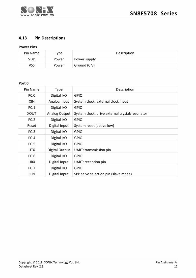
4.13 Pin Descriptions
Power Pins Pin Name Type Description
VDD Power Power supply VSS Power Ground (0 V)
Port 0
Pin Name Type Description P0.0 XIN
Digital I/O Analog Input
GPIO System clock: external clock input
P0.1 XOUT
Digital I/O Analog Output
GPIO System clock: drive external crystal/resonator
P0.2 Reset
Digital I/O Digital Input
GPIO System reset (active low)
P0.3 Digital I/O GPIO P0.4 Digital I/O GPIO P0.5 UTX
Digital I/O Digital Output
GPIO UART: transmission pin
P0.6 URX
Digital I/O Digital Input
GPIO UART: reception pin
P0.7 SSN
Digital I/O Digital Input
GPIO SPI: salve selection pin (slave mode)
Copyright © 2018, SONiX Technology Co., Ltd. Pin Assignments Datasheet Rev. 2.3 12
www.sonix.com.tw SN8F5708 Series
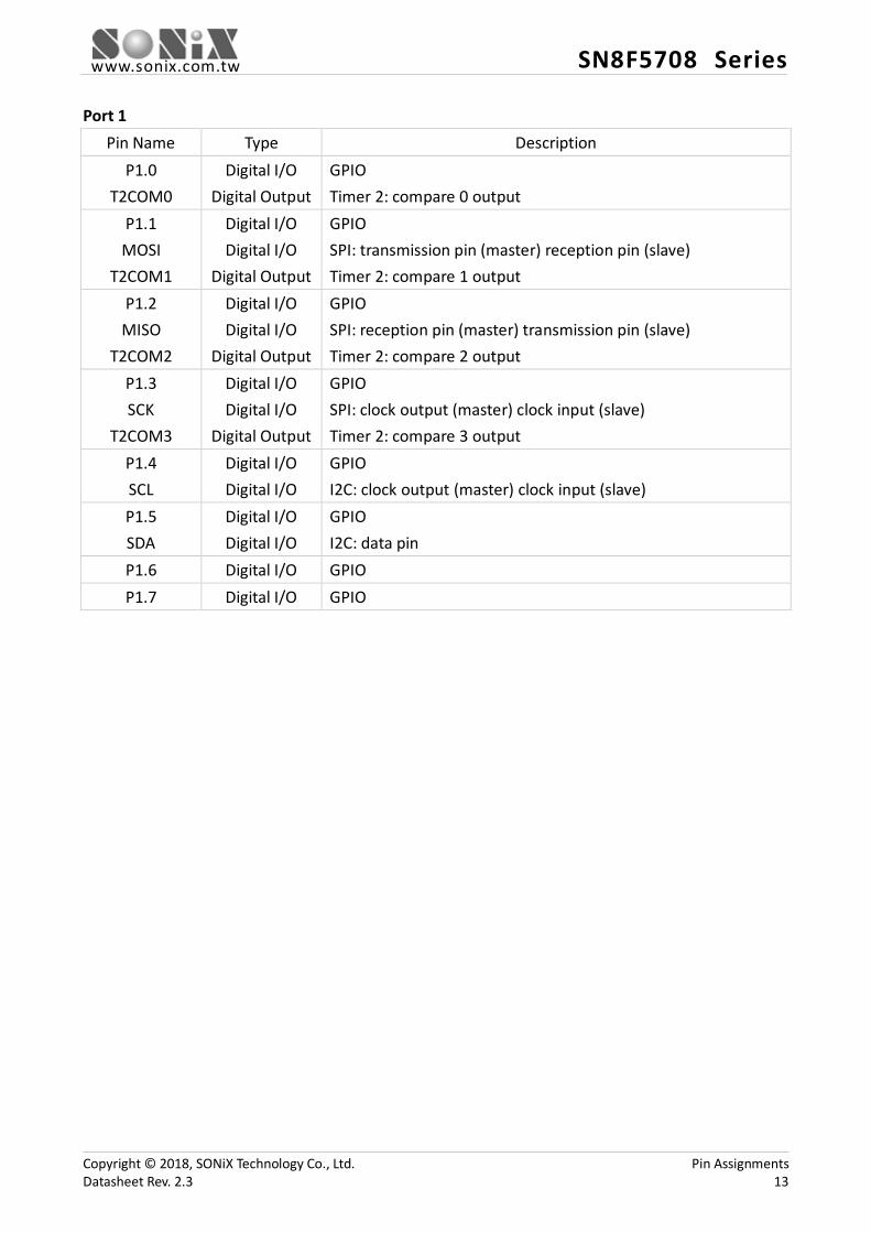
Port 1 Pin Name Type Description
P1.0 T2COM0
Digital I/O Digital Output
GPIO Timer 2: compare 0 output
P1.1 MOSI
T2COM1
Digital I/O Digital I/O
Digital Output
GPIO SPI: transmission pin (master) reception pin (slave) Timer 2: compare 1 output
P1.2 MISO
T2COM2
Digital I/O Digital I/O
Digital Output
GPIO SPI: reception pin (master) transmission pin (slave) Timer 2: compare 2 output
P1.3 SCK
T2COM3
Digital I/O Digital I/O
Digital Output
GPIO SPI: clock output (master) clock input (slave) Timer 2: compare 3 output
P1.4 SCL
Digital I/O Digital I/O
GPIO I2C: clock output (master) clock input (slave)
P1.5 SDA
Digital I/O Digital I/O
GPIO I2C: data pin
P1.6 Digital I/O GPIO P1.7 Digital I/O GPIO
Copyright © 2018, SONiX Technology Co., Ltd. Pin Assignments Datasheet Rev. 2.3 13
www.sonix.com.tw SN8F5708 Series
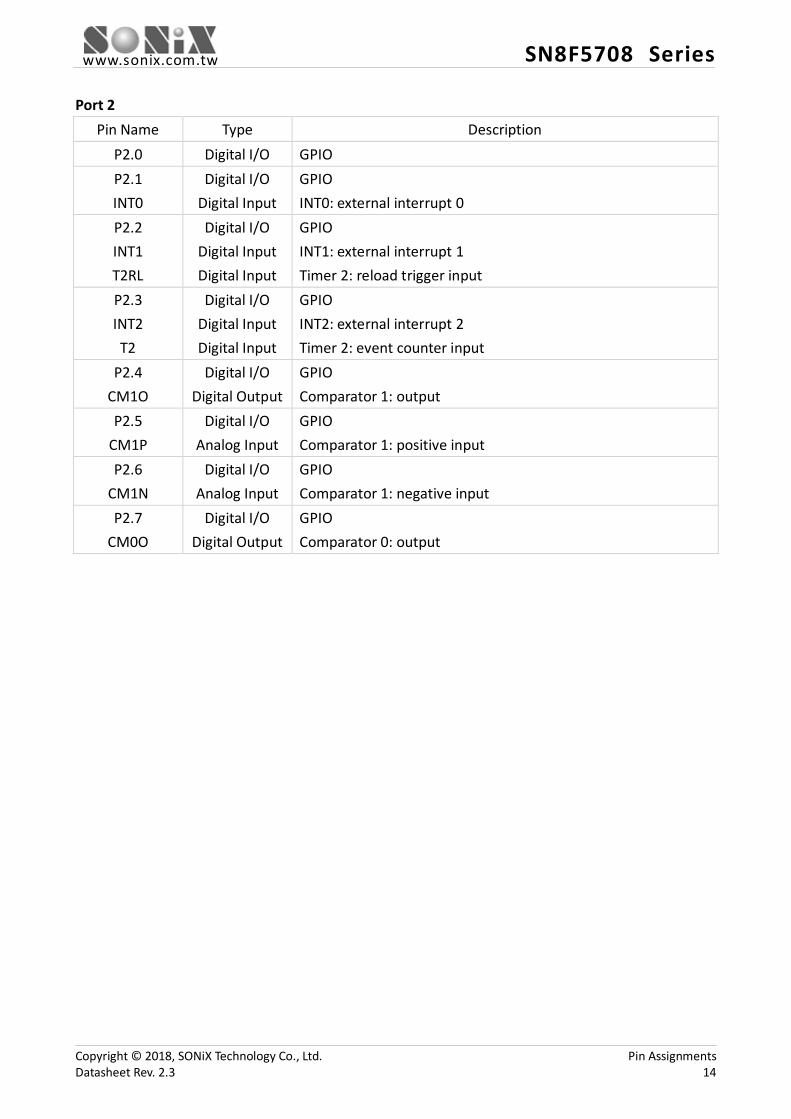
Port 2 Pin Name Type Description
P2.0 Digital I/O GPIO P2.1 INT0
Digital I/O Digital Input
GPIO INT0: external interrupt 0
P2.2 INT1 T2RL
Digital I/O Digital Input Digital Input
GPIO INT1: external interrupt 1 Timer 2: reload trigger input
P2.3 INT2 T2
Digital I/O Digital Input Digital Input
GPIO INT2: external interrupt 2 Timer 2: event counter input
P2.4 CM1O
Digital I/O Digital Output
GPIO Comparator 1: output
P2.5 CM1P
Digital I/O Analog Input
GPIO Comparator 1: positive input
P2.6 CM1N
Digital I/O Analog Input
GPIO Comparator 1: negative input
P2.7 CM0O
Digital I/O Digital Output
GPIO Comparator 0: output
Copyright © 2018, SONiX Technology Co., Ltd. Pin Assignments Datasheet Rev. 2.3 14
www.sonix.com.tw SN8F5708 Series
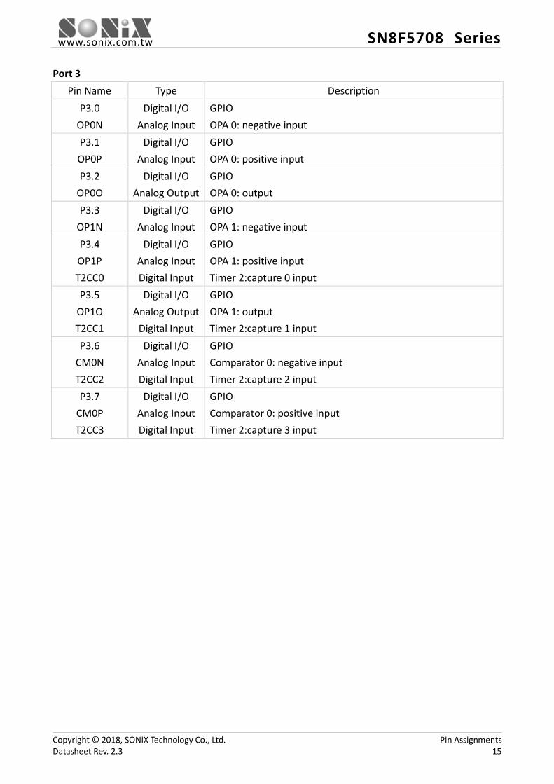
Port 3 Pin Name Type Description
P3.0 OP0N
Digital I/O Analog Input
GPIO OPA 0: negative input
P3.1 OP0P
Digital I/O Analog Input
GPIO OPA 0: positive input
P3.2 OP0O
Digital I/O Analog Output
GPIO OPA 0: output
P3.3 OP1N
Digital I/O Analog Input
GPIO OPA 1: negative input
P3.4 OP1P T2CC0
Digital I/O Analog Input Digital Input
GPIO OPA 1: positive input Timer 2:capture 0 input
P3.5 OP1O T2CC1
Digital I/O Analog Output
Digital Input
GPIO OPA 1: output Timer 2:capture 1 input
P3.6 CM0N T2CC2
Digital I/O Analog Input Digital Input
GPIO Comparator 0: negative input Timer 2:capture 2 input
P3.7 CM0P T2CC3
Digital I/O Analog Input Digital Input
GPIO Comparator 0: positive input Timer 2:capture 3 input
Copyright © 2018, SONiX Technology Co., Ltd. Pin Assignments Datasheet Rev. 2.3 15
www.sonix.com.tw SN8F5708 Series
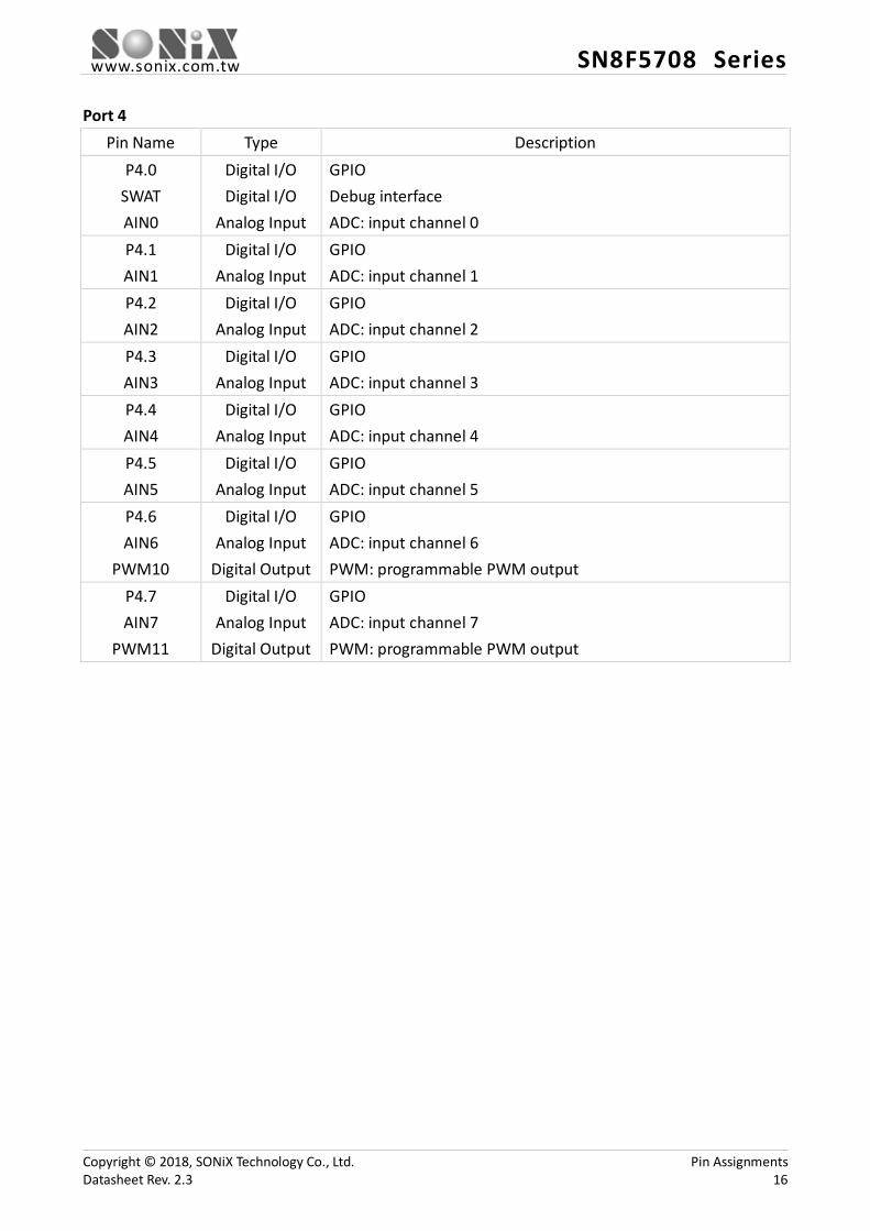
Port 4 Pin Name Type Description
P4.0 SWAT AIN0
Digital I/O Digital I/O
Analog Input
GPIO Debug interface ADC: input channel 0
P4.1 AIN1
Digital I/O Analog Input
GPIO ADC: input channel 1
P4.2 AIN2
Digital I/O Analog Input
GPIO ADC: input channel 2
P4.3 AIN3
Digital I/O Analog Input
GPIO ADC: input channel 3
P4.4 AIN4
Digital I/O Analog Input
GPIO ADC: input channel 4
P4.5 AIN5
Digital I/O Analog Input
GPIO ADC: input channel 5
P4.6 AIN6
PWM10
Digital I/O Analog Input
Digital Output
GPIO ADC: input channel 6 PWM: programmable PWM output
P4.7 AIN7
PWM11
Digital I/O Analog Input
Digital Output
GPIO ADC: input channel 7 PWM: programmable PWM output
Copyright © 2018, SONiX Technology Co., Ltd. Pin Assignments Datasheet Rev. 2.3 16
www.sonix.com.tw SN8F5708 Series
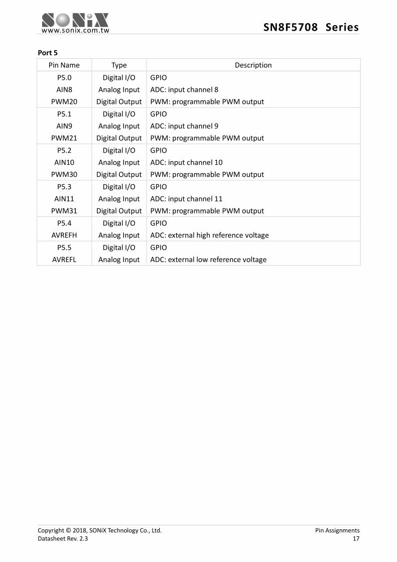
Port 5 Pin Name Type Description
P5.0 AIN8
PWM20
Digital I/O Analog Input
Digital Output
GPIO ADC: input channel 8 PWM: programmable PWM output
P5.1 AIN9
PWM21
Digital I/O Analog Input
Digital Output
GPIO ADC: input channel 9 PWM: programmable PWM output
P5.2 AIN10
PWM30
Digital I/O Analog Input
Digital Output
GPIO ADC: input channel 10 PWM: programmable PWM output
P5.3 AIN11
PWM31
Digital I/O Analog Input
Digital Output
GPIO ADC: input channel 11 PWM: programmable PWM output
P5.4 AVREFH
Digital I/O Analog Input
GPIO ADC: external high reference voltage
P5.5 AVREFL
Digital I/O Analog Input
GPIO ADC: external low reference voltage
Copyright © 2018, SONiX Technology Co., Ltd. Pin Assignments Datasheet Rev. 2.3 17

www.sonix.com.tw SN8F5708 Series
4.14 Pin Characteristic
Port Open- Drain
Sink Current 100mA
VSS+1.5V
Sink Current 20mA
VSS+0.5V
External Interrupt
Wakeup (Level
change) Shared Pin
P0.0 - V - - V XIN P0.1 - V - - V XOUT P0.2 - V - - V RST P0.3 - V - - V P0.4 - V - - V P0.5 V V - - V UTX P0.6 V V - - V URX P0.7 - V - - V SSN P1.0 - V - - V T2COM0 P1.1 V V - - V T2COM1/MOSI P1.2 V V - - V T2COM2/MISO P1.3 V V - - V T2COM3/SCK P1.4 - - V - V SCL P1.5 - - V - V SDA P1.6 - - V - V P1.7 - - V - V P2.0 - - V - - P2.1 - - V V - INT0 P2.2 - - V V - INT1/T2RL P2.3 - - V V - INT2/T2 P2.4 - - V - - CM1O P2.5 - - V - - CM1P P2.6 - - V - - CM1N P2.7 - - V - - CM0O P3.0 - - V - - OP0N P3.1 - - V - - OP0P P3.2 - - V - - OP0O P3.3 - - V - - OP1N P3.4 - - V - - OP1P/T2CC0 P3.5 - - V - - OP1O/T2CC1 P3.6 - - V - - CM0N/T2CC2 P3.7 - - V - - CM0P/T2CC3 P4.0 - - V - - AIN0/SWAT P4.1 - - V - - AIN1 P4.2 - - V - - AIN2 P4.3 - - V - - AIN3 P4.4 - - V - - AIN4 P4.5 - - V - - AIN5 P4.6 - - V - - AIN6/PWM10 P4.7 - - V - - AIN7/PWM11
Copyright © 2018, SONiX Technology Co., Ltd. Pin Assignments Datasheet Rev. 2.3 18
www.sonix.com.tw SN8F5708 Series
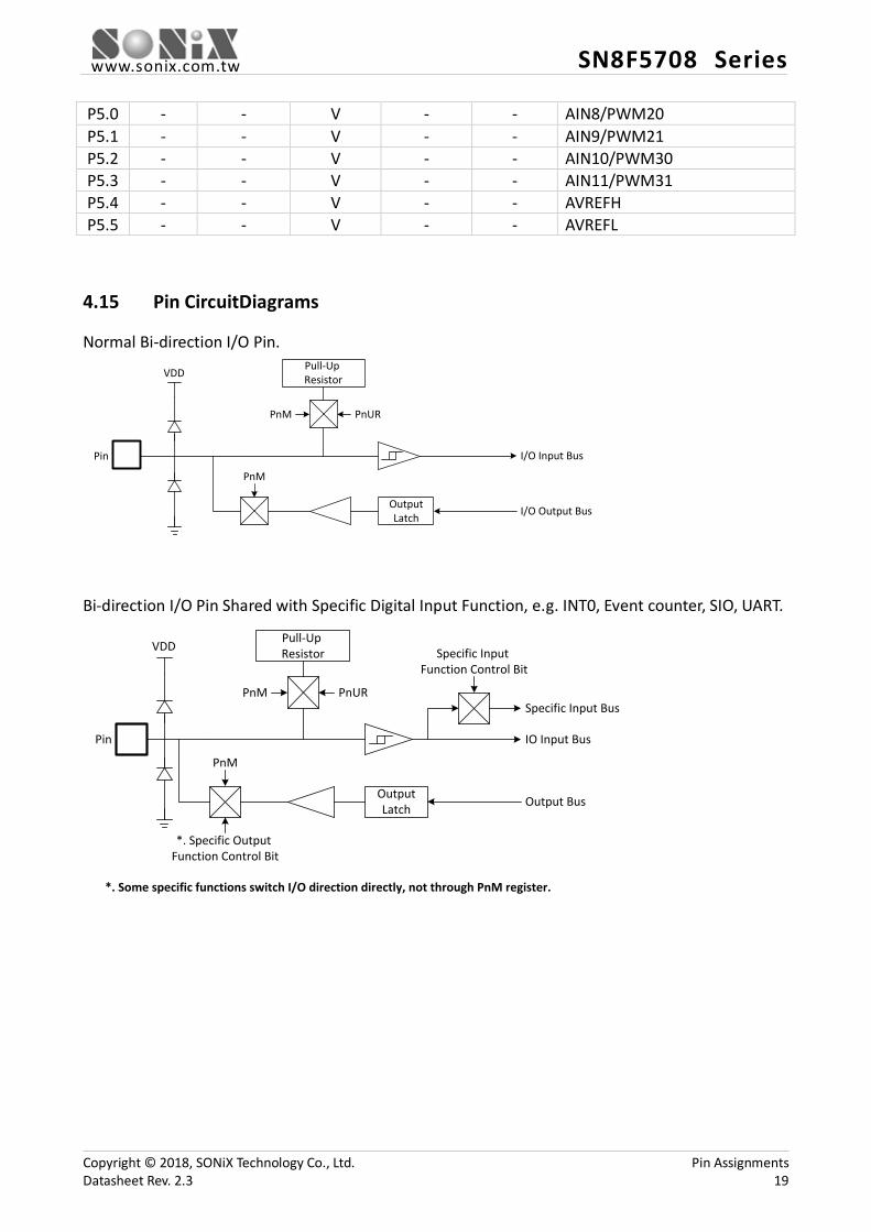
P5.0 - - V - - AIN8/PWM20 P5.1 - - V - - AIN9/PWM21 P5.2 - - V - - AIN10/PWM30 P5.3 - - V - - AIN11/PWM31 P5.4 - - V - - AVREFH P5.5 - - V - - AVREFL
4.15 Pin CircuitDiagrams
Normal Bi-direction I/O Pin. Pull-Up Resistor
OutputLatch
Pin
PnUR
PnM
I/O Input Bus
I/O Output Bus
PnM
VDD
Bi-direction I/O Pin Shared with Specific Digital Input Function, e.g. INT0, Event counter, SIO, UART.
Pull-Up Resistor
OutputLatch
Pin
PnUR
PnM
Specific Input Bus
Output Bus
PnM
Specific Input Function Control Bit
IO Input Bus
*. Specific Output Function Control Bit
*. Some specific functions switch I/O direction directly, not through PnM register.
VDD
Copyright © 2018, SONiX Technology Co., Ltd. Pin Assignments Datasheet Rev. 2.3 19

www.sonix.com.tw SN8F5708 Series
Bi-direction I/O Pin Shared with Specific Digital Output Function, e.g. PWM, SIO, UART.
Pull-Up Resistor
OutputLatch
PnUR
PnM
Output Bus
PnM
IO Input Bus
Specific Output Function Control Bit
Specific Output Bus*. Specific Output Function Control Bit
*. Some specific functions switch I/O direction directly, not through PnM register.
Pin
VDD
Bi-direction I/O Pin Shared with Specific Analog Input Function, e.g. XIN, ADC. Pull-Up Resistor
OutputLatch
PnUR
PnM
I/O Input Bus
I/O Output Bus
PnM*. Specific Analog
Function Control Bit
Analog IP Input Terminal
*. Some specific functions switch I/O direction directly, not through PnM register.
Pin
VDD
Bi-direction I/O Pin Shared with Specific Analog Output Function, e.g. XOUT…
Pull-Up Resistor
OutputLatch
PnUR
PnM
PnM
I/O Input Bus
I/O Output Bus
*. Specific Analog Function Control Bit
Analog IP Output Terminal
*. Some specific functions switch I/O direction directly, not through PnM register.
Pin
VDD
Copyright © 2018, SONiX Technology Co., Ltd. Pin Assignments Datasheet Rev. 2.3 20
www.sonix.com.tw SN8F5708 Series
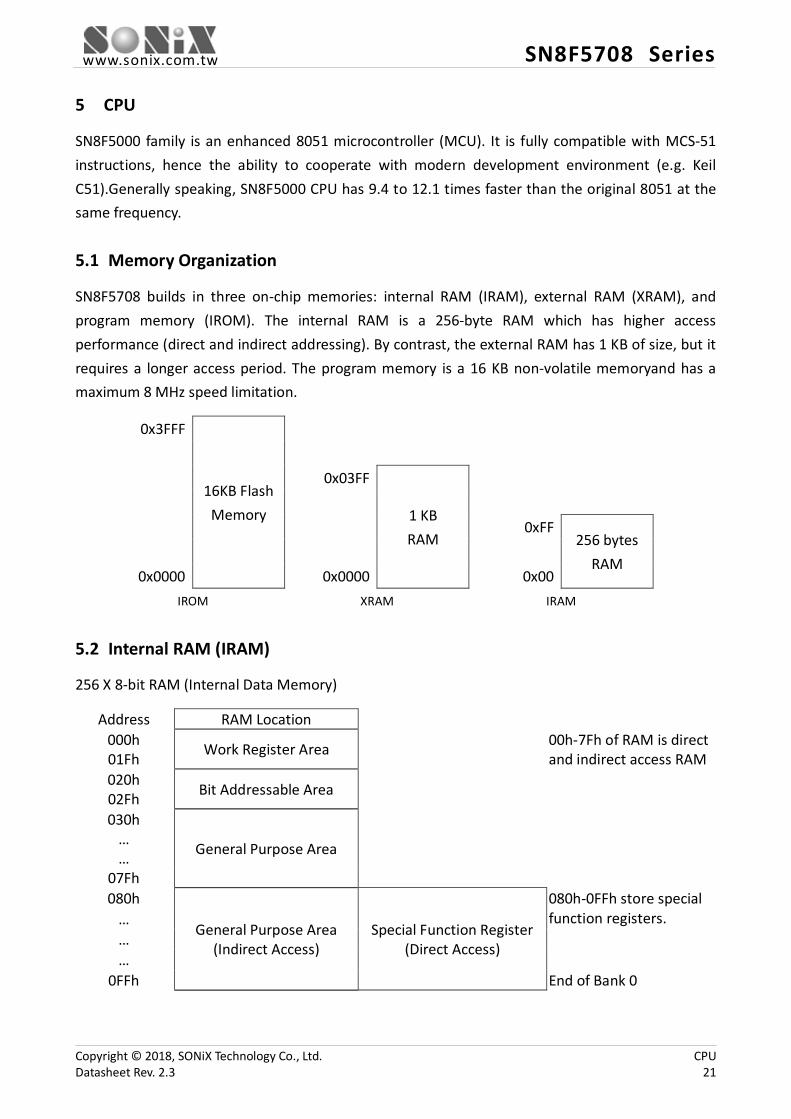
5 CPU
SN8F5000 family is an enhanced 8051 microcontroller (MCU). It is fully compatible with MCS-51 instructions, hence the ability to cooperate with modern development environment (e.g. Keil C51).Generally speaking, SN8F5000 CPU has 9.4 to 12.1 times faster than the original 8051 at the same frequency.
5.1 Memory Organization
SN8F5708 builds in three on-chip memories: internal RAM (IRAM), external RAM (XRAM), and program memory (IROM). The internal RAM is a 256-byte RAM which has higher access performance (direct and indirect addressing). By contrast, the external RAM has 1 KB of size, but it requires a longer access period. The program memory is a 16 KB non-volatile memoryand has a maximum 8 MHz speed limitation.
0x3FFF
16KB Flash Memory
0x03FF
1 KB RAM
0xFF
256 bytes RAM
0x0000 0x0000 0x00 IROM XRAM IRAM
5.2 Internal RAM (IRAM)
256 X 8-bit RAM (Internal Data Memory)
Address RAM Location 000h Work Register Area 00h-7Fh of RAM is direct 01Fh and indirect access RAM 020h Bit Addressable Area 02Fh 030h
… … General Purpose Area
07Fh 080h
General Purpose Area (Indirect Access)
Special Function Register (Direct Access)
080h-0FFh store special function registers. …
… …
0FFh End of Bank 0
Copyright © 2018, SONiX Technology Co., Ltd. CPU Datasheet Rev. 2.3 21
www.sonix.com.tw SN8F5708 Series
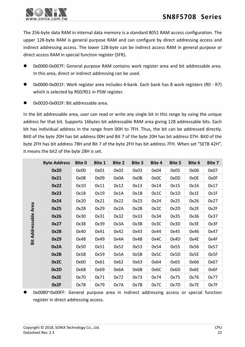
The 256-byte data RAM in internal data memory is a standard 8051 RAM access configuration. The upper 128-byte RAM is general purpose RAM and can configure by direct addressing access and indirect addressing access. The lower 128-byte can be indirect access RAM in general purpose or direct access RAM in special function register (SFR).
0x0000-0x007F: General purpose RAM contains work register area and bit addressable area. In this area, direct or indirect addressing can be used.
0x0000-0x001F: Work register area includes 4-bank. Each bank has 8 work registers (R0 - R7) which is selected by RS0/RS1 in PSW register.
0x0020-0x002F: Bit addressable area.
In the bit addressable area, user can read or write any single bit in this range by using the unique address for that bit. Supports 16bytes bit addressable RAM area giving 128 addressable bits. Each bit has individual address in the range from 00H to 7FH. Thus, the bit can be addressed directly. Bit0 of the byte 20H has bit address 00H and Bit 7 of the byte 20H has bit address 07H. Bit0 of the byte 2FH has bit address 78H and Bit 7 of the byte 2FH has bit address 7FH. When set “SETB 42H”, it means the bit2 of the byte 28H is set.
Bit A
ddre
ssab
le A
rea
Byte Address Bite 0 Bite 1 Bite 2 Bite 3 Bite 4 Bite 5 Bite 6 Bite 7 0x20 0x00 0x01 0x02 0x03 0x04 0x05 0x06 0x07 0x21 0x08 0x09 0x0A 0x0B 0x0C 0x0D 0x0E 0x0F 0x22 0x10 0x11 0x12 0x13 0x14 0x15 0x16 0x17 0x23 0x18 0x19 0x1A 0x1B 0x1C 0x1D 0x1E 0x1F 0x24 0x20 0x21 0x22 0x23 0x24 0x25 0x26 0x27 0x25 0x28 0x29 0x2A 0x2B 0x2C 0x2D 0x2E 0x2F 0x26 0x30 0x31 0x32 0x33 0x34 0x35 0x36 0x37 0x27 0x38 0x39 0x3A 0x3B 0x3C 0x3D 0x3E 0x3F 0x28 0x40 0x41 0x42 0x43 0x44 0x45 0x46 0x47 0x29 0x48 0x49 0x4A 0x4B 0x4C 0x4D 0x4E 0x4F 0x2A 0x50 0x51 0x52 0x53 0x54 0x55 0x56 0x57 0x2B 0x58 0x59 0x5A 0x5B 0x5C 0x5D 0x5E 0x5F 0x2C 0x60 0x61 0x62 0x63 0x64 0x65 0x66 0x67 0x2D 0x68 0x69 0x6A 0x6B 0x6C 0x6D 0x6E 0x6F 0x2E 0x70 0x71 0x72 0x73 0x74 0x75 0x76 0x77 0x2F 0x78 0x79 0x7A 0x7B 0x7C 0x7D 0x7E 0x7F
0x0080~0x00FF: General purpose area in indirect addressing access or special function register in direct addressing access.
Copyright © 2018, SONiX Technology Co., Ltd. CPU Datasheet Rev. 2.3 22
www.sonix.com.tw SN8F5708 Series
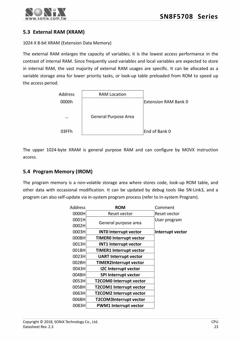
5.3 External RAM (XRAM)
1024 X 8-bit XRAM (Extension Data Memory)
The external RAM enlarges the capacity of variables; it is the lowest access performance in the contrast of internal RAM. Since frequently used variables and local variables are expected to store in internal RAM, the vast majority of external RAM usages are specific. It can be allocated as a variable storage area for lower priority tasks, or look-up table preloaded from ROM to speed up the access period.
Address RAM Location
0000h
General Purpose Area
Extension RAM Bank 0
…
03FFh End of Bank 0
The upper 1024-byte XRAM is general purpose RAM and can configure by MOVX instruction access.
5.4 Program Memory (IROM)
The program memory is a non-volatile storage area where stores code, look-up ROM table, and other data with occasional modification. It can be updated by debug tools like SN-Link3, and a program can also self-update via in-system program process (refer to In-system Program).
Address ROM Comment 0000H Reset vector Reset vector 0001H General purpose area User program 0002H 0003H INT0 Interrupt vector Interrupt vector 000BH TIMER0 Interrupt vector 0013H INT1 Interrupt vector 001BH TIMER1 Interrupt vector 0023H UART Interrupt vector 002BH TIMER2Interrupt vector 0043H I2C Interrupt vector 004BH SPI Interrupt vector 0053H T2COM0 Interrupt vector 005BH T2COM1 Interrupt vector 0063H T2COM2 Interrupt vector 006BH T2COM3Interrupt vector 0083H PWM1 Interrupt vector
Copyright © 2018, SONiX Technology Co., Ltd. CPU Datasheet Rev. 2.3 23
www.sonix.com.tw SN8F5708 Series
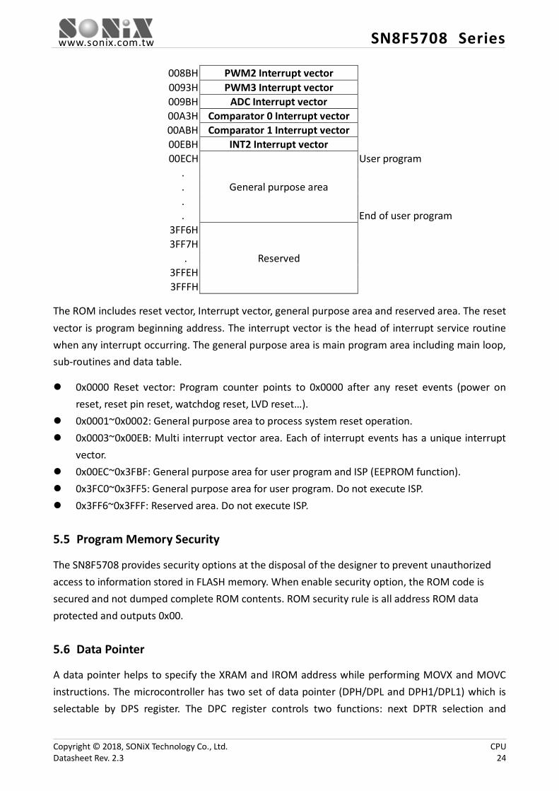
008BH PWM2 Interrupt vector 0093H PWM3 Interrupt vector 009BH ADC Interrupt vector 00A3H Comparator 0 Interrupt vector 00ABH Comparator 1 Interrupt vector 00EBH INT2 Interrupt vector 00ECH
General purpose area
User program . . . . End of user program
3FF6H
Reserved
3FF7H
. 3FFEH 3FFFH
The ROM includes reset vector, Interrupt vector, general purpose area and reserved area. The reset vector is program beginning address. The interrupt vector is the head of interrupt service routine when any interrupt occurring. The general purpose area is main program area including main loop, sub-routines and data table.
0x0000 Reset vector: Program counter points to 0x0000 after any reset events (power on reset, reset pin reset, watchdog reset, LVD reset…).
0x0001~0x0002: General purpose area to process system reset operation. 0x0003~0x00EB: Multi interrupt vector area. Each of interrupt events has a unique interrupt
vector. 0x00EC~0x3FBF: General purpose area for user program and ISP (EEPROM function). 0x3FC0~0x3FF5: General purpose area for user program. Do not execute ISP. 0x3FF6~0x3FFF: Reserved area. Do not execute ISP.
5.5 Program Memory Security
The SN8F5708 provides security options at the disposal of the designer to prevent unauthorized access to information stored in FLASH memory. When enable security option, the ROM code is secured and not dumped complete ROM contents. ROM security rule is all address ROM data protected and outputs 0x00.
5.6 Data Pointer
A data pointer helps to specify the XRAM and IROM address while performing MOVX and MOVC instructions. The microcontroller has two set of data pointer (DPH/DPL and DPH1/DPL1) which is selectable by DPS register. The DPC register controls two functions: next DPTR selection and
Copyright © 2018, SONiX Technology Co., Ltd. CPU Datasheet Rev. 2.3 24
www.sonix.com.tw SN8F5708 Series
automatically increase/decrease DPTR function.
The next DPTR selection can specify which DPTR is anticipated to use after perform MOVX @DPTR instruction. In other word, the DPS can automatically swap between the two data pointers. To enable this function: write 0 to DPSEL and fill 1 to NDPS firstly, then write 1 to DPSEL and fill 0 to NDPS register.
The automatically increase/decrease DPTR function can make an increment or decrement after perform MOVX @DPTR instruction. As a result, it enables a continuous external RAM access without re-specified DPTR value.Those functions are controlled by the DPC Register, where thereare separate DPC register bits for each DPTR, to provide high flexibility in data transfers. The DPC Register address0x93 points to the window where the actual DPC is selected using the DPS Register, same as for the DPTR.
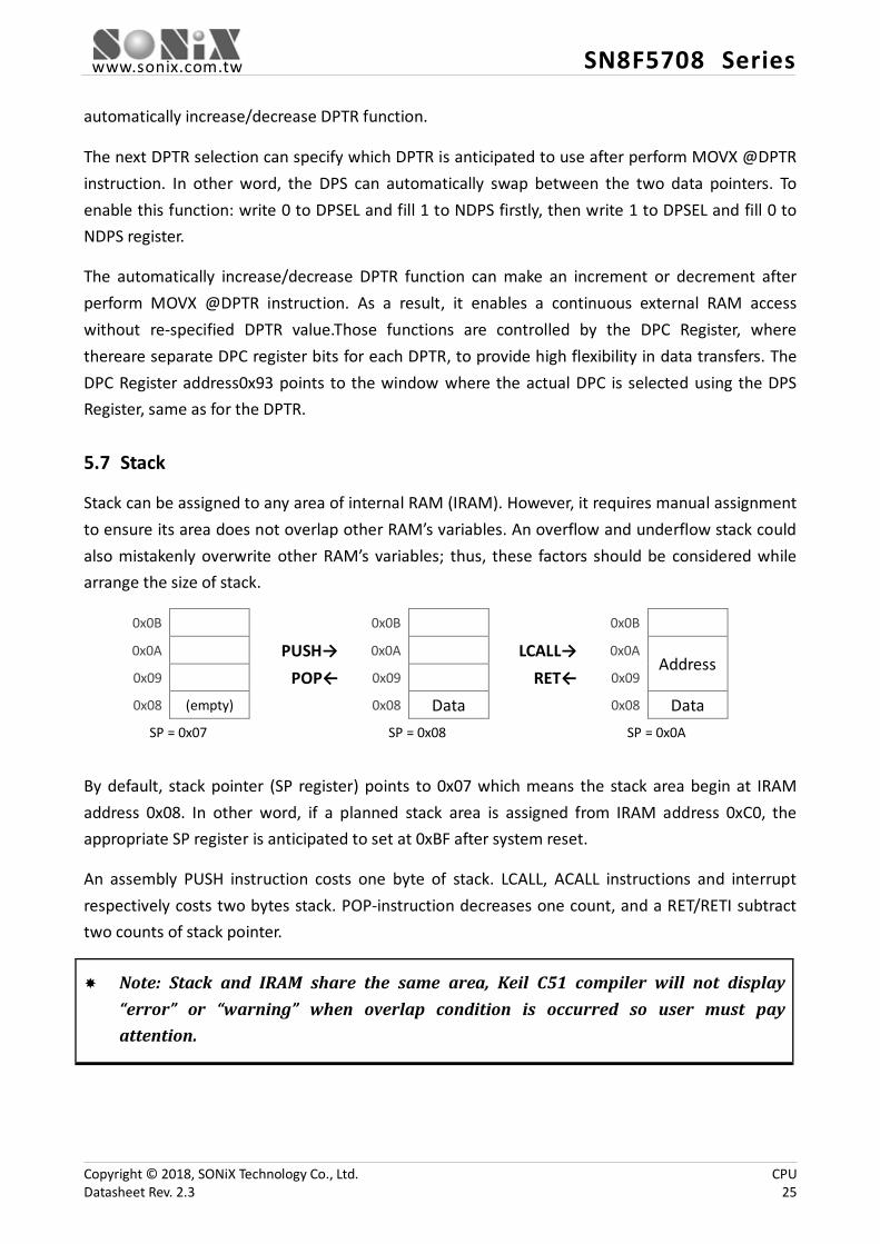
5.7 Stack
Stack can be assigned to any area of internal RAM (IRAM). However, it requires manual assignment to ensure its area does not overlap other RAM’s variables. An overflow and underflow stack could also mistakenly overwrite other RAM’s variables; thus, these factors should be considered while arrange the size of stack.
0x0B 0x0B 0x0B 0x0A PUSH→ 0x0A LCALL→ 0x0A
Address
0x09 POP← 0x09 RET← 0x09 0x08 (empty) 0x08 Data 0x08 Data
SP = 0x07 SP = 0x08 SP = 0x0A
By default, stack pointer (SP register) points to 0x07 which means the stack area begin at IRAM address 0x08. In other word, if a planned stack area is assigned from IRAM address 0xC0, the appropriate SP register is anticipated to set at 0xBF after system reset.
An assembly PUSH instruction costs one byte of stack. LCALL, ACALL instructions and interrupt respectively costs two bytes stack. POP-instruction decreases one count, and a RET/RETI subtract two counts of stack pointer.
Note: Stack and IRAM share the same area, Keil C51 compiler will not display “error” or “warning” when overlap condition is occurred so user must pay attention.
Copyright © 2018, SONiX Technology Co., Ltd. CPU Datasheet Rev. 2.3 25

www.sonix.com.tw SN8F5708 Series
5.8 Stack and Data Pointer Register
Register Bit 7 Bit 6 Bit 5 Bit 4 Bit 3 Bit 2 Bit 1 Bit 0
SP SP7 SP6 SP5 SP4 SP3 SP2 SP1 SP0 DPL DPL7 DPL6 DPL5 DPL4 DPL3 DPL2 DPL1 DPL0 DPH DPH7 DPH6 DPH5 DPH4 DPH3 DPH2 DPH1 DPH0 DPL1 DPL17 DPL16 DPL15 DPL14 DPL13 DPL12 DPL11 DPL10 DPH1 DPH17 DPH16 DPH15 DPH14 DPH13 DPH12 DPH11 DPH10 DPS - - - - - - - DPSEL DPC - - - - NDPS ATMS ATMD ATME
SP Register (0x81) Bit Field Type Initial Description 7..0 SP R/W 0x07 Stack pointer
DPL Register (0x82) Bit Field Type Initial Description 7..0 DPL[7:0] R/W 0x00 Low byte of DPTR0
DPH Register (0x83) Bit Field Type Initial Description 7..0 DPH[7:0] R/W 0x00 High byte of DPTR0
Copyright © 2018, SONiX Technology Co., Ltd. CPU Datasheet Rev. 2.3 26
www.sonix.com.tw SN8F5708 Series
DPL1 Register (0x84) Bit Field Type Initial Description 7..0 DPL1[7:0] R/W 0x00 Low byte of DPTR1
DPH1 Register (0x85) Bit Field Type Initial Description 7..0 DPH1[7:0] R/W 0x00 High byte of DPTR1
DPS Register (0x92) Bit Field Type Initial Description 7..1 Reserved R 0x00 0 DPSEL R/W 0 DPTR selection
0: DPH/DPL (DPTR0) is selected 1: DPH1/DPL1 (DPTR1) is selected
DPC Register (0x93) Bit Field Type Initial Description 7..4 Reserved R 0x0 3 NDPS R/W 0 Next DPTR selection
The DPSEL loads this bit automatically after perform any MOVX @DPTR instruction.
2..1 ATMS/ATMD R/W 00 Automatically increase/decrease DPTR (if ATME applied) 00: +1 after any MOVX @DPTR instruction 01: -1 after any MOVX @DPTR instruction 10: +2 after any MOVX @DPTR instruction 11: -2 after any MOVX @DPTR instruction
0 ATME R/W 0 Automatically increase/decrease DPTR function 0: Disable 1: Enable
Copyright © 2018, SONiX Technology Co., Ltd. CPU Datasheet Rev. 2.3 27

www.sonix.com.tw SN8F5708 Series
6 Special Function Registers
6.1 Special Function Register Memory Map
BIN HEX
000 001 010 011 100 101 110 111
F8 P5 P0M P1M P2M P3M P4M P5M PFLAG
F0 B P0UR P1UR P2UR P3UR P4UR P5UR SRST
E8 P4 MD0 MD1 MD2 MD3 MD4 MD5 ARCON
E0 ACC SPSTA SPCON SPDAT P1OC CLKSEL CLKCMD TCON0
D8 S0CON2 - I2CDAT I2CADR I2CCON I2CSTA SMBSEL SMBDST
D0 PSW IEN4 ADM ADB ADR VREFH P4CON P5CON
C8 T2CON - CRCL CRCH TL2 TH2 CMPT PW3A
C0 IRCON CCEN CCL1 CCH1 CCL2 CCH2 CCL3 CCH3
B8 IEN1 IP1 S0RELH PW1DH PW1DL PW1A PW2A IRCON2
B0 P3 PW3M PW3YL PW3YH PW3BL PW3BH PW3DL PW3DH
A8 IEN0 IP0 S0RELL PW1M PW1YL PW1YH PW1BL PW1BH
A0 P2 PW2M PW2YL PW2YH PW2BL PW2BH PW2DL PW2DH
98 S0CON S0BUF IEN2 OPM CMP0M CMP1M P2CON P3CON
90 P1 P1W DPS DPC PECMD PEROML PEROMH PERAM
88 TCON TMOD TL0 TL1 TH0 TH1 CKCON PEDGE
80 P0 SP DPL DPH DPL1 DPH1 WDTR PCON
Note: All SFRs in the left-most column are bit-addressable. (Every 0x0/0x8-ending SFR addresses are bit-addressable).
Copyright © 2018, SONiX Technology Co., Ltd. Special Function Registers Datasheet Rev. 2.3 28
www.sonix.com.tw SN8F5708 Series
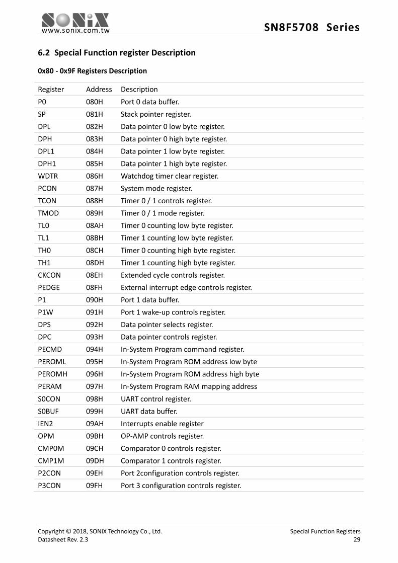
6.2 Special Function register Description
0x80 - 0x9F Registers Description
Register Address Description P0 080H Port 0 data buffer. SP 081H Stack pointer register. DPL 082H Data pointer 0 low byte register. DPH 083H Data pointer 0 high byte register. DPL1 084H Data pointer 1 low byte register. DPH1 085H Data pointer 1 high byte register. WDTR 086H Watchdog timer clear register. PCON 087H System mode register. TCON 088H Timer 0 / 1 controls register. TMOD 089H Timer 0 / 1 mode register. TL0 08AH Timer 0 counting low byte register. TL1 08BH Timer 1 counting low byte register. TH0 08CH Timer 0 counting high byte register. TH1 08DH Timer 1 counting high byte register. CKCON 08EH Extended cycle controls register. PEDGE 08FH External interrupt edge controls register. P1 090H Port 1 data buffer. P1W 091H Port 1 wake-up controls register. DPS 092H Data pointer selects register. DPC 093H Data pointer controls register. PECMD 094H In-System Program command register. PEROML 095H In-System Program ROM address low byte PEROMH 096H In-System Program ROM address high byte PERAM 097H In-System Program RAM mapping address S0CON 098H UART control register. S0BUF 099H UART data buffer. IEN2 09AH Interrupts enable register OPM 09BH OP-AMP controls register. CMP0M 09CH Comparator 0 controls register. CMP1M 09DH Comparator 1 controls register. P2CON 09EH Port 2configuration controls register. P3CON 09FH Port 3 configuration controls register.
Copyright © 2018, SONiX Technology Co., Ltd. Special Function Registers Datasheet Rev. 2.3 29
www.sonix.com.tw SN8F5708 Series
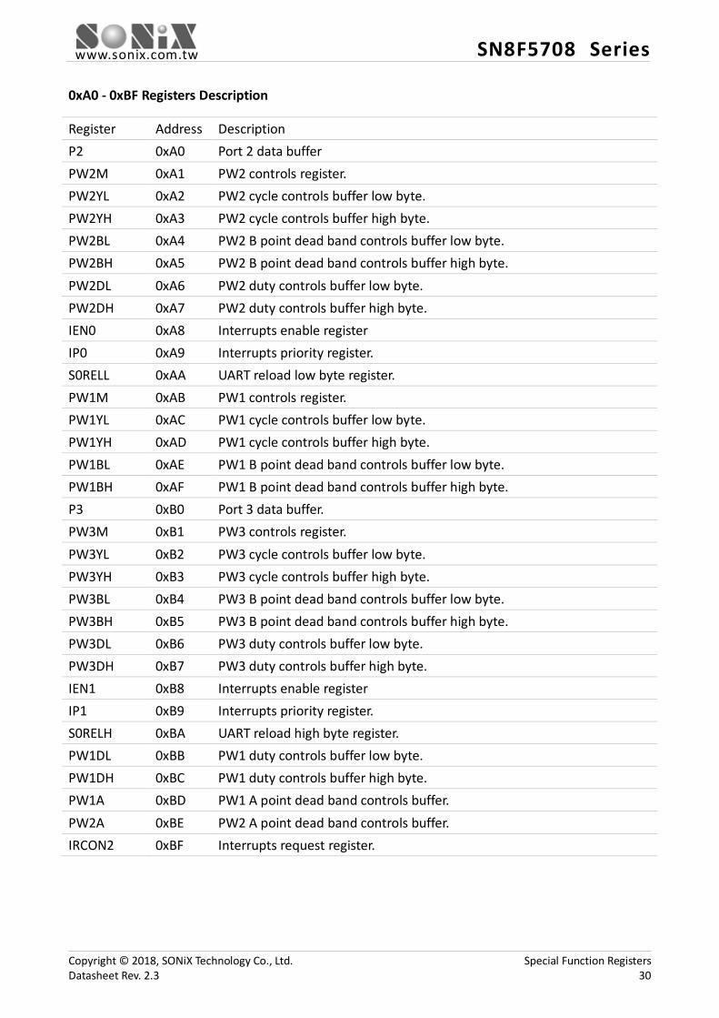
0xA0 - 0xBF Registers Description
Register Address Description P2 0xA0 Port 2 data buffer PW2M 0xA1 PW2 controls register. PW2YL 0xA2 PW2 cycle controls buffer low byte. PW2YH 0xA3 PW2 cycle controls buffer high byte. PW2BL 0xA4 PW2 B point dead band controls buffer low byte. PW2BH 0xA5 PW2 B point dead band controls buffer high byte. PW2DL 0xA6 PW2 duty controls buffer low byte. PW2DH 0xA7 PW2 duty controls buffer high byte. IEN0 0xA8 Interrupts enable register IP0 0xA9 Interrupts priority register. S0RELL 0xAA UART reload low byte register. PW1M 0xAB PW1 controls register. PW1YL 0xAC PW1 cycle controls buffer low byte. PW1YH 0xAD PW1 cycle controls buffer high byte. PW1BL 0xAE PW1 B point dead band controls buffer low byte. PW1BH 0xAF PW1 B point dead band controls buffer high byte. P3 0xB0 Port 3 data buffer. PW3M 0xB1 PW3 controls register. PW3YL 0xB2 PW3 cycle controls buffer low byte. PW3YH 0xB3 PW3 cycle controls buffer high byte. PW3BL 0xB4 PW3 B point dead band controls buffer low byte. PW3BH 0xB5 PW3 B point dead band controls buffer high byte. PW3DL 0xB6 PW3 duty controls buffer low byte. PW3DH 0xB7 PW3 duty controls buffer high byte. IEN1 0xB8 Interrupts enable register IP1 0xB9 Interrupts priority register. S0RELH 0xBA UART reload high byte register. PW1DL 0xBB PW1 duty controls buffer low byte. PW1DH 0xBC PW1 duty controls buffer high byte. PW1A 0xBD PW1 A point dead band controls buffer. PW2A 0xBE PW2 A point dead band controls buffer. IRCON2 0xBF Interrupts request register.
Copyright © 2018, SONiX Technology Co., Ltd. Special Function Registers Datasheet Rev. 2.3 30
www.sonix.com.tw SN8F5708 Series
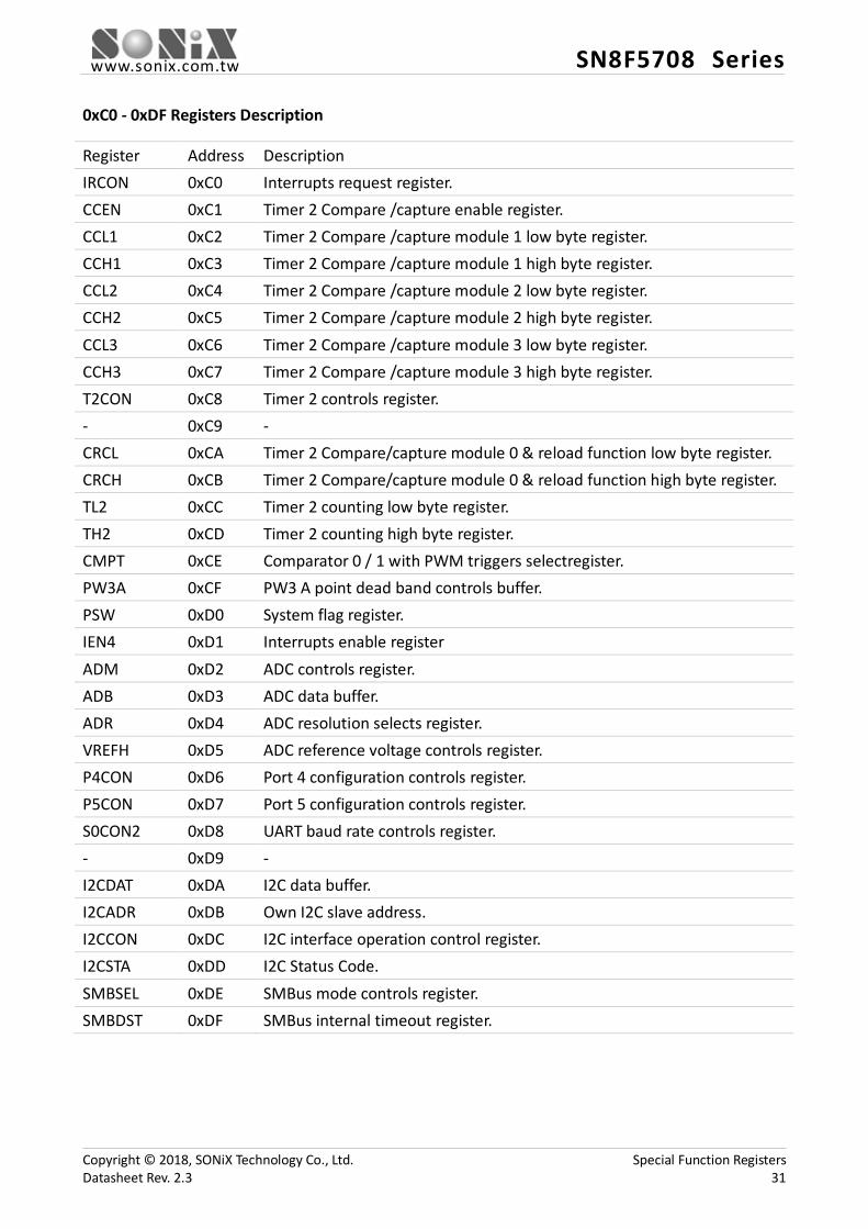
0xC0 - 0xDF Registers Description
Register Address Description IRCON 0xC0 Interrupts request register. CCEN 0xC1 Timer 2 Compare /capture enable register. CCL1 0xC2 Timer 2 Compare /capture module 1 low byte register. CCH1 0xC3 Timer 2 Compare /capture module 1 high byte register. CCL2 0xC4 Timer 2 Compare /capture module 2 low byte register. CCH2 0xC5 Timer 2 Compare /capture module 2 high byte register. CCL3 0xC6 Timer 2 Compare /capture module 3 low byte register. CCH3 0xC7 Timer 2 Compare /capture module 3 high byte register. T2CON 0xC8 Timer 2 controls register. - 0xC9 - CRCL 0xCA Timer 2 Compare/capture module 0 & reload function low byte register. CRCH 0xCB Timer 2 Compare/capture module 0 & reload function high byte register. TL2 0xCC Timer 2 counting low byte register. TH2 0xCD Timer 2 counting high byte register. CMPT 0xCE Comparator 0 / 1 with PWM triggers selectregister. PW3A 0xCF PW3 A point dead band controls buffer. PSW 0xD0 System flag register. IEN4 0xD1 Interrupts enable register ADM 0xD2 ADC controls register. ADB 0xD3 ADC data buffer. ADR 0xD4 ADC resolution selects register. VREFH 0xD5 ADC reference voltage controls register. P4CON 0xD6 Port 4 configuration controls register. P5CON 0xD7 Port 5 configuration controls register. S0CON2 0xD8 UART baud rate controls register. - 0xD9 - I2CDAT 0xDA I2C data buffer. I2CADR 0xDB Own I2C slave address. I2CCON 0xDC I2C interface operation control register. I2CSTA 0xDD I2C Status Code. SMBSEL 0xDE SMBus mode controls register. SMBDST 0xDF SMBus internal timeout register.
Copyright © 2018, SONiX Technology Co., Ltd. Special Function Registers Datasheet Rev. 2.3 31

www.sonix.com.tw SN8F5708 Series
0xE0 - 0xFF Registers Description
Register Address Description ACC 0xE0 Accumulator register. SPSTA 0xE1 SPI statuses register. SPCON 0xE2 SPI control register. SPDAT 0xE3 SPI data buffer. P1OC 0xE4 Open drain controls register. CLKSEL 0xE5 Clock switch selects register. CLKCMD 0xE6 Clock switch controls Register. TCON0 0xE7 Timer 0 / 1 clock controls register. P4 0xE8 Port 4 data buffer. MD0 0xE9 MDU controls register 0. MD1 0xEA MDU controls register 1. MD2 0xEB MDU controls register 2. MD3 0xEC MDU controls register 3. MD4 0xED MDU controls register 4. MD5 0xEE MDU controls register 5. ARCON 0xEF MDU Arithmetic control register. B 0xF0 Multiplication/ division instructiondata buffer. P0UR 0xF1 Port 0 pull-up resister controls register. P1UR 0xF2 Port 1 pull-up resister controls register. P2UR 0xF3 Port 2 pull-up resister controls register. P3UR 0xF4 Port 3 pull-up resister controls register. P4UR 0xF5 Port 4 pull-up resister controls register. P5UR 0xF6 Port 5 pull-up resister controls register. SRST 0xF7 Software reset controlsregister. P5 0xF8 Port 5 data buffer. P0M 0xF9 Port 0 input/output mode register. P1M 0xFA Port 1 input/output mode register. P2M 0xFB Port 2 input/output mode register. P3M 0xFC Port 3 input/output mode register. P4M 0xFD Port 4 input/output mode register. P5M 0xFE Port 5 input/output mode register. PFLAG 0xFF Reset flag register.
Copyright © 2018, SONiX Technology Co., Ltd. Special Function Registers Datasheet Rev. 2.3 32

www.sonix.com.tw SN8F5708 Series
6.3 System Registers
Register Bit 7 Bit 6 Bit 5 Bit 4 Bit 3 Bit 2 Bit 1 Bit 0
ACC ACC7 ACC6 ACC5 ACC4 ACC3 ACC2 ACC1 ACC0 B B7 B6 B5 B4 B3 B2 B1 B0
PSW CY AC F0 RS1 RS0 OV F1 P ACC Register (0xE0) Bit Field Type Initial Description 7..0 ACC[7:0] R/W 0x00 The ACC is an 8-bit data register responsible for
transferring or manipulating data between ALU and data memory. If the result of operating is overflow (OV) or there is carry (C or AC) and parity (P) occurrence, then these flags will be set to PSW register.
B Register (0xF0) Bit Field Type Initial Description 7..0 B[7:0] R/W 0x00 The B register is used during multiplying and division
instructions. It can also be used as a scratch-pad register to hold temporary data.
Copyright © 2018, SONiX Technology Co., Ltd. Special Function Registers Datasheet Rev. 2.3 33

www.sonix.com.tw SN8F5708 Series
PSW Register (0xD0) Bit Field Type Initial Description 7 CY R/W 0 Carry flag.
0: Addition without carry, subtraction with borrowing signal, rotation with shifting out logic “0”, comparison result < 0. 1: Addition with carry, subtraction without borrowing, rotation with shifting out logic “1”, comparison result ≥ 0.
6 AC R/W 0 Auxiliary carry flag. 0: If there is no a carry-out from 3rd bit of Accumulator in BCD operations. 1: If there is a carry-out from 3rd bit of Accumulator in BCD operations.
5 F0 R/W 0 General purpose flag 0. General purpose flag available for user.
4..3 RS[1:0] R/W 00 Register bank select control bit, used to select working register bank. 00: 00H – 07H (Bnak0) 01: 08H – 0FH (Bnak1) 10: 10H – 17H (Bnak2) 11: 18H – 1FH (Bnak3)
2 OV R/W 0 Overflow flag. 0: Non-overflow in Accumulator during arithmetic Operations. 1: overflow in Accumulator during arithmetic Operations.
1 F1 R/W 0 General purpose flag 1. General purpose flag available for user.
0 P R 0 Parity flag. Reflects the number of ‘1’s in the Accumulator. 0: if Accumulator contains an even number of ‘1’s. 1: Accumulator contains an odd number of ‘1’s.
Copyright © 2018, SONiX Technology Co., Ltd. Special Function Registers Datasheet Rev. 2.3 34

www.sonix.com.tw SN8F5708 Series
6.4 RegisterDeclaration
SN8F5708 has many registers to control various functions, but SFR name is not predefined in the C51 / A51 compiler. To make programming easier and therefore need to add header files to declare SFR name.
When using the assembly code programs, please add the following sentence.
1 $NOMOD51;Do not recognize the 8051-specific predefined special register. 2 #include<SN8F5708.H>
When using the C code programs, please add the following sentence.
1 #include<SN8F5708.H>
After adding the header file, user can use name of registers to program. During compilation, the compiler will register name translate into register position through the header file.
Different devices need to use a different header file to declare, but the option file is to use the same.
Device Header file Options file SN8F5705 SN8F5705.h
OPTIONS_SN8F5708.A51
SN8F5707 SN8F5707.h SN8F5708 SN8F5708.h
SN8F570870 SN8F570870.h SN8F57082 SN8F57082.h SN8F57084 SN8F57084.h SN8F57085 SN8F57085.h SN8F57086 SN8F57086.h SN8F57087 SN8F57087.h
Copyright © 2018, SONiX Technology Co., Ltd. Special Function Registers Datasheet Rev. 2.3 35
www.sonix.com.tw SN8F5708 Series
7 Reset and Power-on Controller
The reset and power-on controller has five reset sources: low voltage detectors (LVDs), watchdog, programmable external reset pin, and software reset.The first three sources would trigger an additional power-on sequence. Subsequently, the microcontroller initializes all registers and starts program execution with its reset vector (ROM address 0x0000).
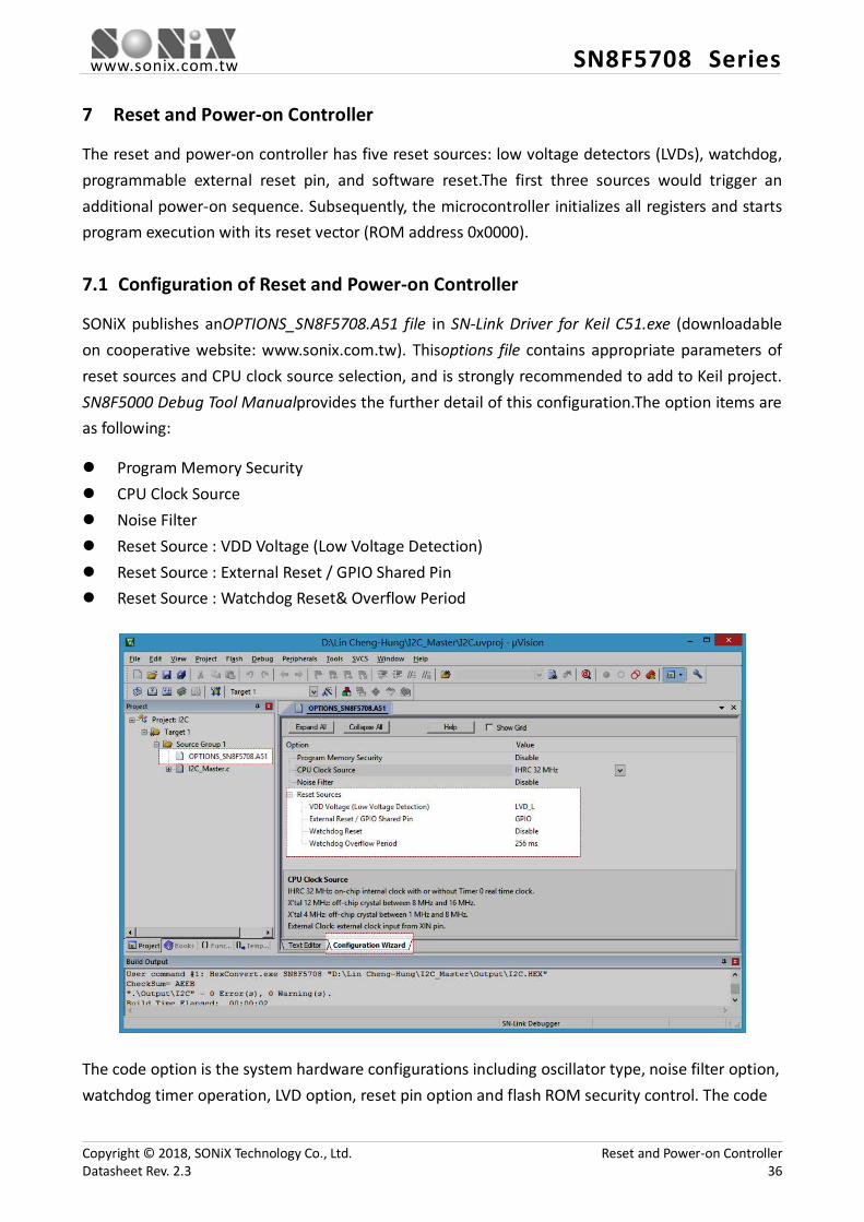
7.1 Configuration of Reset and Power-on Controller
SONiX publishes anOPTIONS_SN8F5708.A51 file in SN-Link Driver for Keil C51.exe (downloadable on cooperative website: www.sonix.com.tw). Thisoptions file contains appropriate parameters of reset sources and CPU clock source selection, and is strongly recommended to add to Keil project. SN8F5000 Debug Tool Manualprovides the further detail of this configuration.The option items are as following:
Program Memory Security CPU Clock Source Noise Filter Reset Source : VDD Voltage (Low Voltage Detection) Reset Source : External Reset / GPIO Shared Pin Reset Source : Watchdog Reset& Overflow Period
The code option is the system hardware configurations including oscillator type, noise filter option, watchdog timer operation, LVD option, reset pin option and flash ROM security control. The code
Copyright © 2018, SONiX Technology Co., Ltd. Reset and Power-on Controller Datasheet Rev. 2.3 36
www.sonix.com.tw SN8F5708 Series
option items are as following table:
Code Option Content Function Description Program Memory Security
Security Disable Disable ROM code Security function Security Enable Enable ROM code Security function
CPU Clock Source IHRC 32MHz High speed internal 32MHz RC. XIN/XOUT pins are bi-direction GPIO mode
IHRC 32MHz with RTC High speed internal 32MH RC with low speed crystal/resonator (e.g. 32.768kHz). Low speed crystal/resonator for Timer 0 real time clock.
X’tal 12MHz High speed crystal /resonator (e.g. 12MHz) for external high clock oscillator
X’tal 4MHz Standard crystal /resonator (e.g. 4M) for external high clock oscillator
External Clock XIN pin connect external clock (1M ~32M), XOUT pin is bi-direction GPIO mode
Noise Filter Disable Disable Noise Filter Enable Enable Noise Filter
LVD LVD_L LVD will reset chip if VDD is below 1.8V. LVD_M LVD will reset chip if VDD is below 1.8V. The
LVD24 flag will indicate if VDD is below 2.4V. LVD_H LVD will reset chip if VDD is below 2.4V. The
LVD33 flag will indicate if VDD is below 3.3V. LVD_Max LVD will reset chip if VDD is below 3.3V
External Reset Reset with De-bounce Enable External reset pin with De-bounce Reset without De-bounce Enable External reset pin without De-bounce GPIO with P02 Enable P02
Watchdog Reset Always Watchdog timer is always on enable even in STOP mode and IDLE mode
Enable Enable watchdog timer. Watchdog timer stops in STOP mode and IDLE mode
Disable Disable Watchdog function Watchdog Overflow Period
64ms Watchdog timer clock source FILRC /4 128ms Watchdog timer clock source FILRC /8 256ms Watchdog timer clock source FILRC /16 512ms Watchdog timer clock source FILRC /32
Copyright © 2018, SONiX Technology Co., Ltd. Reset and Power-on Controller Datasheet Rev. 2.3 37

www.sonix.com.tw SN8F5708 Series
7.2 Power-on Sequence
A power-on sequence would be triggered by LVD, watchdog, and external reset pin. It takes place between the end of reset signal and program execution. Overall, it includes two stages: power stabilization period, and clock stabilization period.
VDD
VSS
VDD
VSS
Watchdog Normal Run
Watchdog Stop
System Normal Run
System Stop
LVD Detect Level
External Reset Low Detect
External Reset High Detect Watchdog
Overflow
WatchdogReset Delay Time
ExternalReset Delay Time
Power OnDelay Time
Power
External Reset
Watchdog Reset
System Status
The power stabilization period spends 5 msin typical condition. Afterward the microcontroller fetches CPU Clock Source selection automatically. The selected clock source would be driven, and the system counts 4096 times of the clock period to ensure its reliability.
Note: In high power noise environment, user can put 10ohm resistor in the front of 0.1uF capacitor& VDD PAD to suppress power noise and avoid IC damage.
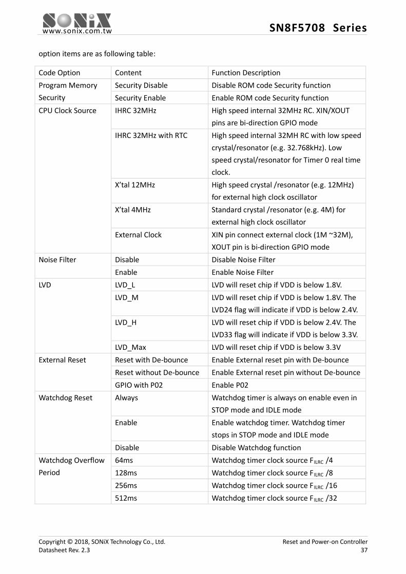
7.3 LVD Reset
The low voltage detectors monitor VDD pin’s voltage at three levels: 1.8 V, 2.4 V and 3.3 V. Depend on low voltage detection configuration, the comparison result can be seen as a system reset signal, or simply as LVD24/LVD33 register flags. The table below lists four different low voltage detection configurations, from LVD_Max to LVD_L, and the respectively results of VDD pin’s condition.
Copyright © 2018, SONiX Technology Co., Ltd. Reset and Power-on Controller Datasheet Rev. 2.3 38
www.sonix.com.tw SN8F5708 Series
VDD
VSS
System Normal Run
System Stop
LVD Detect Voltage
Power OnDelay Time
Power
System Status
Power is below LVD Detect Voltage and System Reset.
Condition LVD_Max LVD_H LVD_M LVD_L VDD ≤ 3.3 V Reset LVD33 = 1 - - VDD ≤ 2.4 V Reset Reset LVD24 = 1 - VDD ≤ 1.8 V Reset Reset Reset Reset
7.4 Watchdog Reset
Watchdog is a periodic reset signal generator for the purpose of monitoring the execution flow.Its internal timer is expected to be cleared in a check point ofprogram flow; therefore, the actual reset signal would be generated only after a software problem occurs. Writing 0x5A to WDTR is the proper method to place a check point in program.
1 WDTR = 0x5A;
Watchdog timer interval time = 256 * 1/ (Internal Low-Speed oscillator frequency/WDT Pre-scalar) = 256 / (FILR C/WDT Pre-scaler) …sec
Internal low-speed oscillator
WDT pre-scaler
Watchdog interval time
FILRC=16 kHz
FILRC/4 256/(16000/4)=64ms FILRC/8 256/(16000/8)=128ms
FILRC/16 256/(16000/16)=256ms FILRC/32 256/(16000/32)=512ms
The operation mode of watchdog is configurable in options file: Always mode counts its internal timer in all CPU operation modes (normal, IDLE, SLEEP); Enable mode counts its internal timer during CPU stays in normal mode, and it would not trigger watchdog reset in IDLE and STOP modes; Disable mode suspends its internal timer at all CPU modes, and the watchdog would not trigger in this condition.
Copyright © 2018, SONiX Technology Co., Ltd. Reset and Power-on Controller Datasheet Rev. 2.3 39
www.sonix.com.tw SN8F5708 Series
When watchdog is operating in always mode, the system will consume additional power.
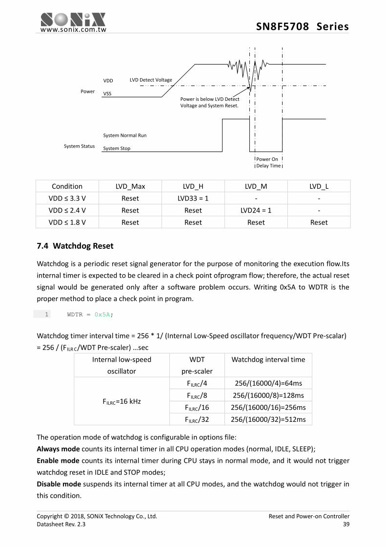
7.5 External Reset Pin
Programmable external reset pin is configurable in options file. Once it is enabled, it monitors its shared pin’s logic level. A logical low (lower than 30% of VDD) would immediatelytrigger system reset until the input is recovered to high (lager than 70% of VDD).
An optional de-bounce period can improve reset signal’s stability. Instead of immediate reset, the system reset requires an8-ms-long logic low to avoid bouncing from a button key. Any signal lower than de-bounce period would not affect the CPU’s execution.
MCU
VDD
VSS
VCC
GND
RST
R147K ohm
C10.1uF
R2
100 ohmMCU
VDD
VSS
VCC
GND
RST
R147K ohm
C10.1uF
DIODE
R2
100 ohm
Note:
1. The reset circuit is no any protection against unusual power or brown out reset on the left side of the figure.
2. The R2 100 ohm resistor of “Simply reset circuit” and “Diode & RC reset circuit” is necessary to limit any current flowing into reset pin from external capacitor C in the event of reset pin breakdown due to Electrostatic Discharge (ESD) or Electrical Over-stress (EOS) on the right side of the figure.
Copyright © 2018, SONiX Technology Co., Ltd. Reset and Power-on Controller Datasheet Rev. 2.3 40
www.sonix.com.tw SN8F5708 Series
7.6 Software Reset
A software reset would be generated after consecutively set SRSTREQ register.As a result, this procedure enables firmware’sabilityto reset microcontroller (e.g. reset after firmware update). The following sample C code repeatedly set the least bit of SRST register to perform software reset.
1 2
SRST = 0x01; SRST = 0x01;
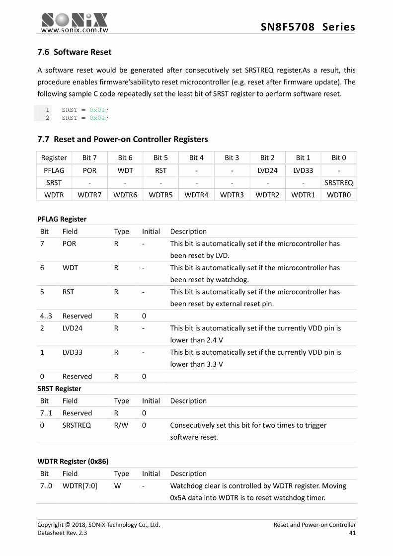
7.7 Reset and Power-on Controller Registers
Register Bit 7 Bit 6 Bit 5 Bit 4 Bit 3 Bit 2 Bit 1 Bit 0
PFLAG POR WDT RST - - LVD24 LVD33 - SRST - - - - - - - SRSTREQ
WDTR WDTR7 WDTR6 WDTR5 WDTR4 WDTR3 WDTR2 WDTR1 WDTR0 PFLAG Register Bit Field Type Initial Description 7 POR R - This bit is automatically set if the microcontroller has
been reset by LVD. 6 WDT R - This bit is automatically set if the microcontroller has
been reset by watchdog. 5 RST R - This bit is automatically set if the microcontroller has
been reset by external reset pin. 4..3 Reserved R 0 2 LVD24 R - This bit is automatically set if the currently VDD pin is
lower than 2.4 V 1 LVD33 R - This bit is automatically set if the currently VDD pin is
lower than 3.3 V 0 Reserved R 0
SRST Register Bit Field Type Initial Description 7..1 Reserved R 0 0 SRSTREQ R/W 0 Consecutively set this bit for two times to trigger
software reset. WDTR Register (0x86) Bit Field Type Initial Description 7..0 WDTR[7:0] W - Watchdog clear is controlled by WDTR register. Moving
0x5A data into WDTR is to reset watchdog timer.
Copyright © 2018, SONiX Technology Co., Ltd. Reset and Power-on Controller Datasheet Rev. 2.3 41

www.sonix.com.tw SN8F5708 Series
8 System Clock and Power Management
For power saving purpose, the microcontroller built in three different operation modes: normal, IDLE, and STOP mode.
The normal mode means that CPU and peripheral functions are under normally execution.The system clock is based on the combination of source selection, clock divider, and program memory wait state.IDLE mode is the situation that temporarily suspends CPU clock and its execution, yet it remains peripherals’functionality (e.g. timers, PWM, SPI, UART, and I2C). By contrast, STOP mode disables all functions and clock generator until a wakeup signal to return normal mode.
8.1 System Clock
The microcontroller includes an on-chip clock generator (IHRC 32MHz), crystal/resonator driver, and an external clock input. The reset and power-on controller automatically loads clock source selection during power-on sequence. Therefore, the selected clock source is seen as ‘fosc’ domain which is a fixed frequency at any time.
Subsequently, the selected clock source (fosc) is divided by 1 to 128 times which is controlled by CLKSEL register. The CPU input the divided clock as its operation base (named fcpu).Applying CLKSEL's setting when CLKCMD register be written0x69.
1 2 3 4
CKCON = 0x70; // For change safely the system clock CLKSEL = 0x05; //set fcpu = fosc / 4
CLKCMD = 0x69; //Apply CLKSEL’s setting CKCON = 0x00; // IROM fetch = fcpu / 1
foscMUX
Divider÷1 to ÷128
IHRC 32MHz
Crystal
External Clock
Clock Source Selection(set in Options file)
CLKSEL
fcpu
CPU
ROMinterface
CKCON
IROM
ROM interface is built in between CPU and IROM (program memory). It optionally extends the data fetching cycle in order to support lower speed program memory.
IROM fetching cycle (Instruction cycle) ≦ 8MHz
Copyright © 2018, SONiX Technology Co., Ltd. System Clock and Power Management Datasheet Rev. 2.3 42
www.sonix.com.tw SN8F5708 Series
Note: For user develop program in C language or assembly,the first line of the program “must be set” CLKSEL= 0x07~0x00, CLKMD= 0x69 and then setCKCON= 0x00~0x70, this priority cannot be modified.
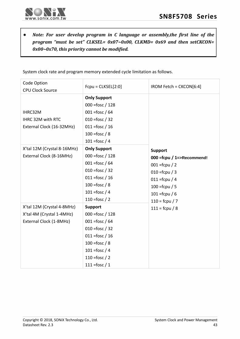
System clock rate and program memory extended cycle limitation as follows.
Code Option CPU Clock Source
Fcpu = CLKSEL[2:0] IROM Fetch = CKCON[6:4]
IHRC32M IHRC 32M with RTC External Clock (16-32MHz)
Only Support 000 =fosc / 128 001 =fosc / 64 010 =fosc / 32 011 =fosc / 16 100 =fosc / 8 101 =fosc / 4
Support 000 =fcpu / 1=>Recommend! 001 =fcpu / 2 010 =fcpu / 3 011 =fcpu / 4 100 =fcpu / 5 101 =fcpu / 6 110 = fcpu / 7 111 = fcpu / 8
X’tal 12M (Crystal 8-16MHz) External Clock (8-16MHz)
Only Support 000 =fosc / 128 001 =fosc / 64 010 =fosc / 32 011 =fosc / 16 100 =fosc / 8 101 =fosc / 4 110 =fosc / 2
X’tal 12M (Crystal 4-8MHz) X’tal 4M (Crystal 1-4MHz) External Clock (1-8MHz)
Support 000 =fosc / 128 001 =fosc / 64 010 =fosc / 32 011 =fosc / 16 100 =fosc / 8 101 =fosc / 4 110 =fosc / 2 111 =fosc / 1
Copyright © 2018, SONiX Technology Co., Ltd. System Clock and Power Management Datasheet Rev. 2.3 43
www.sonix.com.tw SN8F5708 Series
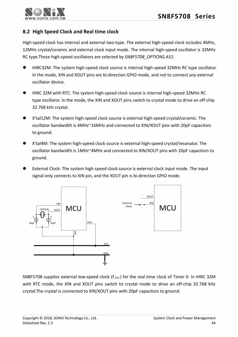
8.2 High Speed Clock and Real time clock
High-speed clock has internal and external two-type. The external high-speed clock includes 4MHz, 12MHz crystal/ceramic and external clock input mode. The internal high-speed oscillator is 32MHz RC type.These high-speed oscillators are selected by SN8F5708_OPTIONS.A51.
IHRC32M: The system high-speed clock source is internal high-speed 32MHz RC type oscillator. In the mode, XIN and XOUT pins are bi-direction GPIO mode, and not to connect any external oscillator device.
IHRC 32M with RTC: The system high-speed clock source is internal high-speed 32MHz RC type oscillator. In the mode, the XIN and XOUT pins switch to crystal mode to drive an off-chip 32.768 kHz crystal.
X’tal12M: The system high-speed clock source is external high-speed crystal/ceramic. The oscillator bandwidth is 4MHz~16MHz and connected to XIN/XOUT pins with 20pF capacitors to ground.
X’tal4M: The system high-speed clock source is external high-speed crystal/resonator. The oscillator bandwidth is 1MHz~4MHz and connected to XIN/XOUT pins with 20pF capacitors to ground.
External Clock: The system high-speed clock source is external clock input mode. The input signal only connects to XIN pin, and the XOUT pin is bi-direction GPIO mode.
MCU
VCC
GND
C
20pF
XIN
XOUT
VDD
VSS
C
20pF
CRYSTAL
MCUXIN
XOUT
External Clock
SN8F5708 supplies external low-speed clock (f RTC) for the real time clock of Timer 0. In IHRC 32M with RTC mode, the XIN and XOUT pins switch to crystal mode to drive an off-chip 32.768 kHz crystal.The crystal is connected to XIN/XOUT pins with 20pF capacitors to ground.
Copyright © 2018, SONiX Technology Co., Ltd. System Clock and Power Management Datasheet Rev. 2.3 44
www.sonix.com.tw SN8F5708 Series
8.3 Noise Filter
The Noise Filter controlled by NoiseFilter option is a low pass filter and supports crystal mode. The purpose is to filter high rate noise coupling on high clock signal from external oscillator. In high noisy environment, enable NoiseFilter option is the strongly recommendation to reduce noise effect.
8.4 Power Management
After the end of reset signal and power-on sequence, the CPU starts program execution at the speed of fcpu. Overall, the CPU and all peripherals are functional in this situation (categorized as normal mode).
The least two bits of PCON register (IDLE at bit 0 and STOP at bit 1) control the microcontroller’s power management unit.
If IDLE bit is set by program, only CPU clock source would be gated. Consequently, peripheral functions (such as timers, PWM, and I2C) and clock generator (IHRC 32 MHz/crystal driver) remain execution in this status. Any change from P0/P1 input and interrupt events can make the microcontroller turns back to normal mode, and the IDLE bit would be cleared automatically.
Any function can work in IDLE mode. Only CPU is suspended The IDLE mode wake-up sources are P0/P1 level change trigger and any interrupt event.
If STOP bit is set, by contrast, CPU, peripheral functions, and clock generator are suspended. Data storage in registers and RAM would be kept in this mode. Any change from P0/P1 can wake up the microcontroller and resume system’s execution. STOP bit would be cleared automatically.
CPU, peripheral functions, and clock generator are suspended. The STOP mode wake-up source is P0/P1 level change trigger.
For user who is develop program in C language, IDLE and STOP macros is strongly recommended to control the microcontroller’s system mode, instead of set IDLE and STOP bits directly.
1 2
IDLE(); STOP();
Note: Into IDLE mode or STOP mode by “Assembly Language” must be using MOV instruction.
Copyright © 2018, SONiX Technology Co., Ltd. System Clock and Power Management Datasheet Rev. 2.3 45
www.sonix.com.tw SN8F5708 Series
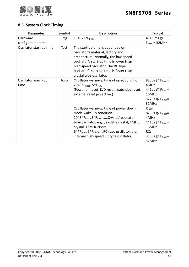
8.5 System Clock Timing
Parameter Symbol Description Typical Hardware configuration time
Tcfg 131072*FIHRC 4.096ms @ FIHRC = 32MHz
Oscillator start up time Tost The start-up time is depended on oscillator’s material, factory and architecture. Normally, the low-speed oscillator’s start-up time is lower than high-speed oscillator. The RC type oscillator’s start-up time is faster than crystal type oscillator.
-
Oscillator warm-up time
Tosp Oscillator warm-up time of reset condition. 2048*Fhosc+ 5*FILRC
(Power on reset, LVD reset, watchdog reset, external reset pin active.)
825us @ Fhosc= 4MHz 441us @ Fhosc= 16MHz 377us @ Fhosc= 32MHz
Oscillator warm-up time of power down mode wake-up condition. 2048*Fhosc+5*FILRC ……Crystal/resonator type oscillator, e.g. 32768Hz crystal, 4MHz crystal, 16MHz crystal…
64*Fhosc+5*FILRC……RC type oscillator, e.g. internal high-speed RC type oscillator.
X’tal: 825us @ Fhosc= 4MHz 441us @ Fhosc= 16MHz RC: 315us @ Fhosc= 32MHz
Copyright © 2018, SONiX Technology Co., Ltd. System Clock and Power Management Datasheet Rev. 2.3 46

www.sonix.com.tw SN8F5708 Series
Power On Reset Timing
External Reset Pin Reset Timing
Watchdog Reset Timing
STOP Mode Wake-up Timing
Vdd
Power On ResetFlag
Oscillator
Fcpu(Instruction Cycle)
Tcfg Tost Tosp
Vp
External Reset Pin
Oscillator
Fcpu(Instruction Cycle)
Tcfg Tost Tosp
Reset pin falling edge trigger system reset.
Reset pin returns to high status.
System is under resetstatus.
External ResetFlag
Watchdog ResetFlag
Oscillator
Fcpu(Instruction Cycle)
Tcfg Tost Tosp
Watchdog timer overflow.
Wake-up PinRising Edge
Oscillator
Fcpu(Instruction Cycle)
TospTost
Wake-up PinFalling Edge
System inserts into power down mode.
Edge trigger system wake-up.
Copyright © 2018, SONiX Technology Co., Ltd. System Clock and Power Management Datasheet Rev. 2.3 47

www.sonix.com.tw SN8F5708 Series
IDLE Mode Wake-up Timing
Oscillator Start-up Time The start-up time is depended on oscillator’s material, factory and architecture. Normally, the low-speed oscillator’s start-up time is lower than high-speed oscillator.
Low Speed Crystal (32K, 455K)
Tost
Crystal
Tost
RC Oscillator
Tost
Ceramic/Resonator
Tost
Wake-up PinRising Edge
Oscillator
Fcpu(Instruction Cycle)
Wake-up PinFalling Edge
System inserts into green mode.
Edge trigger system wake-up.
0x000xFF0xFE 0x01 0x02 ...0xFD... ... ... ... ...Timer
Timer overflow.
Copyright © 2018, SONiX Technology Co., Ltd. System Clock and Power Management Datasheet Rev. 2.3 48
www.sonix.com.tw SN8F5708 Series
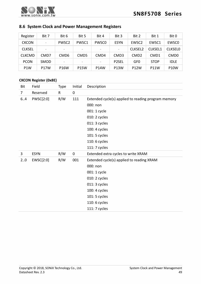
8.6 System Clock and Power Management Registers
Register Bit 7 Bit 6 Bit 5 Bit 4 Bit 3 Bit 2 Bit 1 Bit 0
CKCON - PWSC2 PWSC1 PWSC0 ESYN EWSC2 EWSC1 EWSC0
CLKSEL - - - - - CLKSEL2 CLKSEL1 CLKSEL0 CLKCMD CMD7 CMD6 CMD5 CMD4 CMD3 CMD2 CMD1 CMD0
PCON SMOD - - - P2SEL GF0 STOP IDLE P1W P17W P16W P15W P14W P13W P12W P11W P10W
CKCON Register (0x8E) Bit Field Type Initial Description 7 Reserved R 0 6..4 PWSC[2:0] R/W 111 Extended cycle(s) applied to reading program memory
000: non 001: 1 cycle 010: 2 cycles 011: 3 cycles 100: 4 cycles 101: 5 cycles 110: 6 cycles 111: 7 cycles
3 ESYN R/W 0 Extended extra cycles to write XRAM 2..0 EWSC[2:0] R/W 001 Extended cycle(s) applied to reading XRAM
000: non 001: 1 cycle 010: 2 cycles 011: 3 cycles 100: 4 cycles 101: 5 cycles 110: 6 cycles 111: 7 cycles
Copyright © 2018, SONiX Technology Co., Ltd. System Clock and Power Management Datasheet Rev. 2.3 49
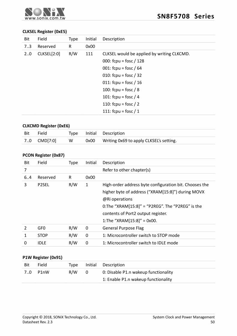
www.sonix.com.tw SN8F5708 Series
CLKSEL Register (0xE5) Bit Field Type Initial Description 7..3 Reserved R 0x00 2..0 CLKSEL[2:0] R/W 111 CLKSEL would be applied by writing CLKCMD.
000: fcpu = fosc / 128 001: fcpu = fosc / 64 010: fcpu = fosc / 32 011: fcpu = fosc / 16 100: fcpu = fosc / 8 101: fcpu = fosc / 4 110: fcpu = fosc / 2 111: fcpu = fosc / 1
CLKCMD Register (0xE6) Bit Field Type Initial Description 7..0 CMD[7:0] W 0x00 Writing 0x69 to apply CLKSEL’s setting.
PCON Register (0x87) Bit Field Type Initial Description 7 Refer to other chapter(s) 6..4 Reserved R 0x00 3 P2SEL R/W 1 High-order address byte configuration bit. Chooses the
higher byte of address (“XRAM[15:8]”) during MOVX @Ri operations 0:The “XRAM[15:8]” = “P2REG”. The “P2REG” is the contents of Port2 output register. 1:The “XRAM[15:8]” = 0x00.
2 GF0 R/W 0 General Purpose Flag 1 STOP R/W 0 1: Microcontroller switch to STOP mode 0 IDLE R/W 0 1: Microcontroller switch to IDLE mode
P1W Register (0x91) Bit Field Type Initial Description 7..0 P1nW R/W 0 0: Disable P1.n wakeup functionality
1: Enable P1.n wakeup functionality
Copyright © 2018, SONiX Technology Co., Ltd. System Clock and Power Management Datasheet Rev. 2.3 50
www.sonix.com.tw SN8F5708 Series
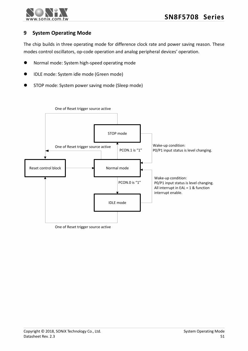
9 System Operating Mode
The chip builds in three operating mode for difference clock rate and power saving reason. These modes control oscillators, op-code operation and analog peripheral devices’ operation.
Normal mode: System high-speed operating mode
IDLE mode: System idle mode (Green mode)
STOP mode: System power saving mode (Sleep mode)
Reset control block Normal mode
IDLE mode
STOP mode
One of Reset trigger source active
One of Reset trigger source active
Wake-up condition:P0/P1 input status is level changing.PCON.1 is “1”
PCON.0 is “1”Wake-up condition:P0/P1 input status is level changing.All interrupt in EAL = 1 & function interrupt enable.
One of Reset trigger source active
Copyright © 2018, SONiX Technology Co., Ltd. System Operating Mode Datasheet Rev. 2.3 51

www.sonix.com.tw SN8F5708 Series
The operating mode clock control as following table:
OperatingMode Normal Mode IDLE Mode STOP Mode
IHRC IHRC: Running Ext. OSC: Disable
IHRC: Running Ext. OSC: Disable
Stop
ILRC Running Running Watchdog always: Running Other : stop
Ext. OSC IHRC: Disable Ext. OSC : Running
IHRC: Disable Ext. OSC : Running
Stop
CPU instruction Executing Stop Stop
Timer 0 (Timer, Event counter)
Active by TR0 Active by TR0 Inactive
Timer 1 (Timer, Event counter)
Active by TR1 Active by TR1 Inactive
Timer 2 (Timer, capture, T2COM)
Active as enable Active as enable Inactive
PWM1 Active as enable Active as enable Inactive
PWM2 Active as enable Active as enable Inactive
PWM3 Active as enable Active as enable Inactive
UART Active as enable Active as enable Inactive
SPI Active as enable Active as enable Inactive
I2C Active as enable Active as enable Inactive
ADC Active as enable Active as enable Inactive
Comparator 0 Active as enable Active as enable Active as enable
Comparator 1 Active as enable Active as enable Active as enable
OPA Active as enable Active as enable Active as enable
Watchdog timer By Watchdog Code option
By Watchdog Code option
By Watchdog Code option
Internal interrupt All active All active All inactive
External interrupt All active All active All inactive
Wakeup source -
P0, P1, Reset,All interrupt inEAL = 1 & function interrupt enable
P0, P1, Reset
Ext.OSC: External high/low-speed oscillator (XIN/XOUT). IHRC: Internal high-speed oscillator RC type. ILRC: Internal low-speed oscillator RC type.
Copyright © 2018, SONiX Technology Co., Ltd. System Operating Mode Datasheet Rev. 2.3 52
www.sonix.com.tw SN8F5708 Series
9.1 Normal Mode
The Normal Mode is system high clock operating mode. The system clock source is from high speed oscillator. The program is executed. After power on and any reset trigger released, the system inserts into normal mode to execute program. When the system is wake-up from STOP/IDLE mode, the system also inserts into normal mode. In normal mode, the high speed oscillator is active, and the power consumption is largest of all operating modes.
The program is executed, and full functions are controllable. The system rate is high speed. The high speed oscillator and internal low speed RC type oscillator are active. Normal mode can be switched to other operating modes through PCON register. STOP/IDLE mode is wake-up to normal mode.
9.2 STOP Mode
The STOP mode is the system ideal status. No program execution and oscillator operation. Only internal regulator is active to keep all control gates status, register status and SRAM contents. The STOP mode is waked up by P0/P1 hardware level change trigger. P0 wake-up function is always enables. The STOP mode is wake-up to normal mode. Inserting STOP mode is controlled by stop bit of PCON register. When stop = 1, the system inserts into STOP Mode. After system wake-up from STOP mode, the stop bit is disabled (zero status) automatically.
The program stops executing, and full functions are disabled. All oscillators including external high/low speed oscillator, internal high speed oscillator and
internal low speed oscillator stop. Only internal regulator is active to keep all control gates status, register status and SRAM
contents. The system inserts into normal mode after wake-up from STOP mode. The STOP mode wake-up source is P0/P1 level change trigger.
Copyright © 2018, SONiX Technology Co., Ltd. System Operating Mode Datasheet Rev. 2.3 53
www.sonix.com.tw SN8F5708 Series
9.3 IDLE Mode
The IDLE mode is another system ideal status not like STOP mode. In STOP mode, all functions and hardware devices are disabled. But in IDLE mode, the system clock source keeps running, so the power consumption of IDLE mode is larger than STOP mode. In IDLE mode, the program isn’t executed, but the timer with wake-up function is active as enabled, and the timer clock source is the non-stop system clock. The IDLE mode has 2 wake-up sources. One is the P0/P1 level change trigger wake-up. The other one is any interrupt in EAL = 1 & function interrupt enable. That’s mean users can setup any function with interrupt enable, and the system is waked up until the interrupt issue. Inserting IDLE mode is controlled by idle bit of PCON register. When idle = 1, the system inserts into IDLE mode. After system wake-up from IDLE mode, the idle bit is disabled (zero status) automatically.
The program stops executing, and full functions are disabled. Only the timer with wake-up function is active. The oscillator to be the system clock source keeps running, and the other oscillators operation
is depend on system operation mode configuration. If inserting IDLE mode from normal mode, the system insets to normal mode after wake-up. The IDLE mode wake-up sources are P0/P1 level change trigger. If the function clock source is system clock, the functions are workable as enabled and under
IDLE mode, e.g. Timer, PWM, event counter… All interrupt inEAL = 1 & function interrupt enable can wake-up in IDLE mode.
Copyright © 2018, SONiX Technology Co., Ltd. System Operating Mode Datasheet Rev. 2.3 54
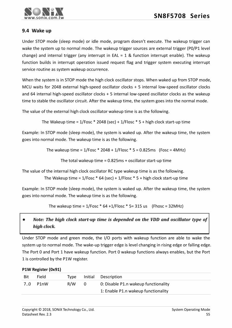
www.sonix.com.tw SN8F5708 Series
9.4 Wake up
Under STOP mode (sleep mode) or idle mode, program doesn’t execute. The wakeup trigger can wake the system up to normal mode. The wakeup trigger sources are external trigger (P0/P1 level change) and internal trigger (any interrupt in EAL = 1 & function interrupt enable). The wakeup function builds in interrupt operation issued request flag and trigger system executing interrupt service routine as system wakeup occurrence.
When the system is in STOP mode the high clock oscillator stops. When waked up from STOP mode, MCU waits for 2048 external high-speed oscillator clocks + 5 internal low-speed oscillator clocks and 64 internal high-speed oscillator clocks + 5 internal low-speed oscillator clocks as the wakeup time to stable the oscillator circuit. After the wakeup time, the system goes into the normal mode.
The value of the external high clock oscillator wakeup time is as the following.
The Wakeup time = 1/Fosc * 2048 (sec) + 1/Flosc * 5 + high clock start-up time
Example: In STOP mode (sleep mode), the system is waked up. After the wakeup time, the system goes into normal mode. The wakeup time is as the following.
The wakeup time = 1/Fosc * 2048 + 1/Flosc * 5 = 0.825ms (Fosc = 4MHz)
The total wakeup time = 0.825ms + oscillator start-up time
The value of the internal high clock oscillator RC type wakeup time is as the following. The Wakeup time = 1/Fosc * 64 (sec) + 1/Flosc * 5 + high clock start-up time
Example: In STOP mode (sleep mode), the system is waked up. After the wakeup time, the system goes into normal mode. The wakeup time is as the following.
The wakeup time = 1/Fosc * 64 +1/Flosc * 5= 315 us (Fhosc = 32MHz)
Note: The high clock start-up time is depended on the VDD and oscillator type of high clock.
Under STOP mode and green mode, the I/O ports with wakeup function are able to wake the system up to normal mode. The wake-up trigger edge is level changing in rising edge or falling edge. The Port 0 and Port 1 have wakeup function. Port 0 wakeup functions always enables, but the Port 1 is controlled by the P1W register.
P1W Register (0x91) Bit Field Type Initial Description 7..0 P1nW R/W 0 0: Disable P1.n wakeup functionality
1: Enable P1.n wakeup functionality
Copyright © 2018, SONiX Technology Co., Ltd. System Operating Mode Datasheet Rev. 2.3 55
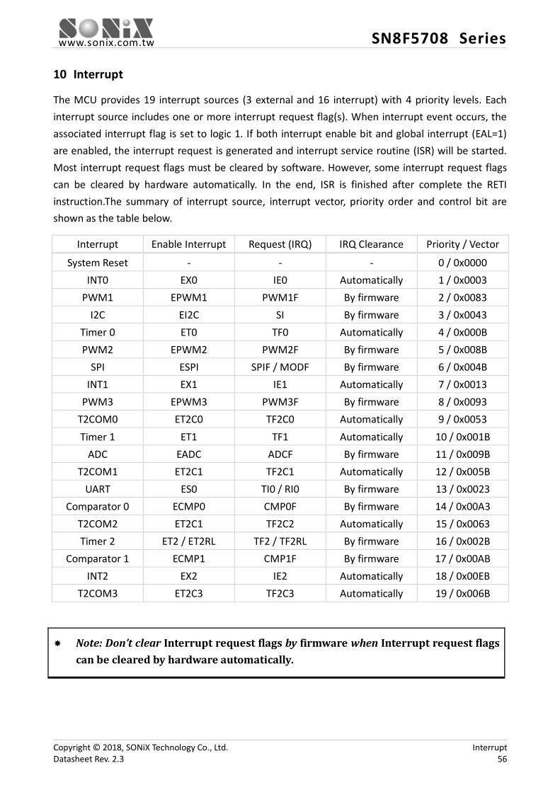
www.sonix.com.tw SN8F5708 Series
10 Interrupt
The MCU provides 19 interrupt sources (3 external and 16 interrupt) with 4 priority levels. Each interrupt source includes one or more interrupt request flag(s). When interrupt event occurs, the associated interrupt flag is set to logic 1. If both interrupt enable bit and global interrupt (EAL=1) are enabled, the interrupt request is generated and interrupt service routine (ISR) will be started. Most interrupt request flags must be cleared by software. However, some interrupt request flags can be cleared by hardware automatically. In the end, ISR is finished after complete the RETI instruction.The summary of interrupt source, interrupt vector, priority order and control bit are shown as the table below.
Interrupt Enable Interrupt Request (IRQ) IRQ Clearance Priority / Vector
System Reset - - - 0 / 0x0000 INT0 EX0 IE0 Automatically 1 / 0x0003
PWM1 EPWM1 PWM1F By firmware 2 / 0x0083 I2C EI2C SI By firmware 3 / 0x0043
Timer 0 ET0 TF0 Automatically 4 / 0x000B PWM2 EPWM2 PWM2F By firmware 5 / 0x008B
SPI ESPI SPIF / MODF By firmware 6 / 0x004B INT1 EX1 IE1 Automatically 7 / 0x0013
PWM3 EPWM3 PWM3F By firmware 8 / 0x0093 T2COM0 ET2C0 TF2C0 Automatically 9 / 0x0053 Timer 1 ET1 TF1 Automatically 10 / 0x001B
ADC EADC ADCF By firmware 11 / 0x009B T2COM1 ET2C1 TF2C1 Automatically 12 / 0x005B
UART ES0 TI0 / RI0 By firmware 13 / 0x0023 Comparator 0 ECMP0 CMP0F By firmware 14 / 0x00A3
T2COM2 ET2C1 TF2C2 Automatically 15 / 0x0063 Timer 2 ET2 / ET2RL TF2 / TF2RL By firmware 16 / 0x002B
Comparator 1 ECMP1 CMP1F By firmware 17 / 0x00AB INT2 EX2 IE2 Automatically 18 / 0x00EB
T2COM3 ET2C3 TF2C3 Automatically 19 / 0x006B
Note: Don’t clear Interrupt request flags by firmware when Interrupt request flags can be cleared by hardware automatically.
Copyright © 2018, SONiX Technology Co., Ltd. Interrupt Datasheet Rev. 2.3 56

www.sonix.com.tw SN8F5708 Series
10.1 Interrupt Operation
Interrupt operation is controlled by interrupt request flag and interrupt enable bits. Interrupt request flag is interrupt source event indicator, no matter what interrupt function status (enable or disable). Both interrupt enable bit and global interrupt (EAL=1) are enabled, the system executes interrupt operation when each of interrupt request flags actives. The program counter points to interrupt vector (0x03 – 0xEB) and execute ISR.
10.2 Interrupt Priority
Each interrupt source has its specific default priority order. If two interrupts occurs simultaneously, the higher priority ISR will be service first. The lower priority ISR will be serviced after the higher priority ISR completes. The next ISR will be service after the previous ISR complete, no matter the priority order.
For special priority needs, 4-level priority levels (Level 0 – Level 3) are used. All interrupt sources are classified into 6 priority groups (Group0 – Group5). Each group can be set one specific priority level. Priority level is selected by IP0/IP1 registers. Level 3 is the highest priority and Level 0 is the lowest. The interrupt sources inside the same group will share the same priority level. With the same priority level, the priority rule follows default priority.
Priority Level IP1.x IP0.x Level 0 0 0 Level 1 0 1 Level 2 1 0 Level 3 1 1
The ISR with the higher priority level can be serviced first; even can break the on-going ISR with the lower priority level. The ISR with the lower priority level will be pending until the ISR with the higher priority level completes.
Group Interrupt Source Group 0 INT0 PWM1 I2C Group 1 Timer 0 PWM2 SPI Group 2 INT1 PWM3 T2COM0 Group 3 Timer 1 ADC T2COM1 Group 4 UART Comparator 0 T2COM2 Group 5 Timer 2 Comparator 1 INT2 T2COM3
Copyright © 2018, SONiX Technology Co., Ltd. Interrupt Datasheet Rev. 2.3 57

www.sonix.com.tw SN8F5708 Series
When more than one interrupt request occur, the highest priority request must be executed first. Choose the highest priority request according natural priority and priority level. The steps are as the following: 1. Choose the groups which have the highest priority level between all groups. 2. Choose the group which is the highest nature priority between the groups with the highest
priority level. 3. Choose the ISR which has the highest nature priority inside the group with the highest
priority.
Group 0
Group 1
Group 2
Group 3
Interrupt Group
Group 4
Group 5
Interrupt Priority
High
Low
All groups within the same priority level
Level 3
Level 2
Level 1
Level 0
Priority LevelInterrupt Priority
High
Low
Higher priority level has higher priorityIP0.0 = IP0.1 = IP0.2 = IP0.3 = IP0.4 = IP0.5IP1.0 = IP1.1 = IP1.2 = IP1.3 = IP1.4 = IP1.5
As the example, group5 has the highest priority level and group0~group2 have the lowest priority level. It means the interrupt vector in group5 has the highest interrupt priority, the 2nd interrupt priority in group4 and the 3rd interrupt priority in group3. Group0~ group2 have the same priority level thus the nature priority rule will be followed. Therefore, interrupt priority will be group5> group4> group3> group0> group1> group2.
MOV IP0, #00101000B ; Set group0 - group5 in different priority level. MOV IP0, #00110000B
Group 5
Group 4
Group 3
Group 0
Interrupt Group
Group 1
Group 2
Interrupt Priority
High
Low
Priority Level: GP5>GP4>GP3=GP2=GP1=GP0
Interrupt Priority: GP5>GP4>GP3>GP0>GP1>GP2
Priority Level
11
10
01
00
00
00
Copyright © 2018, SONiX Technology Co., Ltd. Interrupt Datasheet Rev. 2.3 58
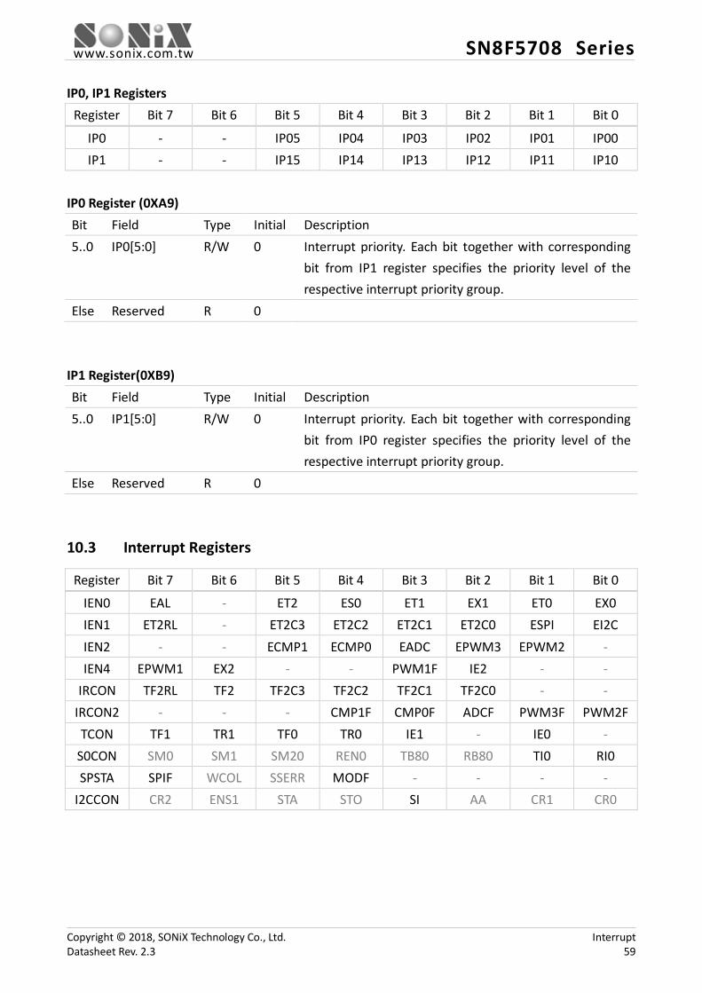
www.sonix.com.tw SN8F5708 Series
IP0, IP1 Registers Register Bit 7 Bit 6 Bit 5 Bit 4 Bit 3 Bit 2 Bit 1 Bit 0
IP0 - - IP05 IP04 IP03 IP02 IP01 IP00 IP1 - - IP15 IP14 IP13 IP12 IP11 IP10
IP0 Register (0XA9) Bit Field Type Initial Description 5..0 IP0[5:0] R/W 0 Interrupt priority. Each bit together with corresponding
bit from IP1 register specifies the priority level of the respective interrupt priority group.
Else Reserved R 0 IP1 Register(0XB9) Bit Field Type Initial Description 5..0 IP1[5:0] R/W 0 Interrupt priority. Each bit together with corresponding
bit from IP0 register specifies the priority level of the respective interrupt priority group.
Else Reserved R 0
10.3 Interrupt Registers
Register Bit 7 Bit 6 Bit 5 Bit 4 Bit 3 Bit 2 Bit 1 Bit 0
IEN0 EAL - ET2 ES0 ET1 EX1 ET0 EX0 IEN1 ET2RL - ET2C3 ET2C2 ET2C1 ET2C0 ESPI EI2C IEN2 - - ECMP1 ECMP0 EADC EPWM3 EPWM2 - IEN4 EPWM1 EX2 - - PWM1F IE2 - -
IRCON TF2RL TF2 TF2C3 TF2C2 TF2C1 TF2C0 - - IRCON2 - - - CMP1F CMP0F ADCF PWM3F PWM2F TCON TF1 TR1 TF0 TR0 IE1 - IE0 -
S0CON SM0 SM1 SM20 REN0 TB80 RB80 TI0 RI0 SPSTA SPIF WCOL SSERR MODF - - - -
I2CCON CR2 ENS1 STA STO SI AA CR1 CR0
Copyright © 2018, SONiX Technology Co., Ltd. Interrupt Datasheet Rev. 2.3 59
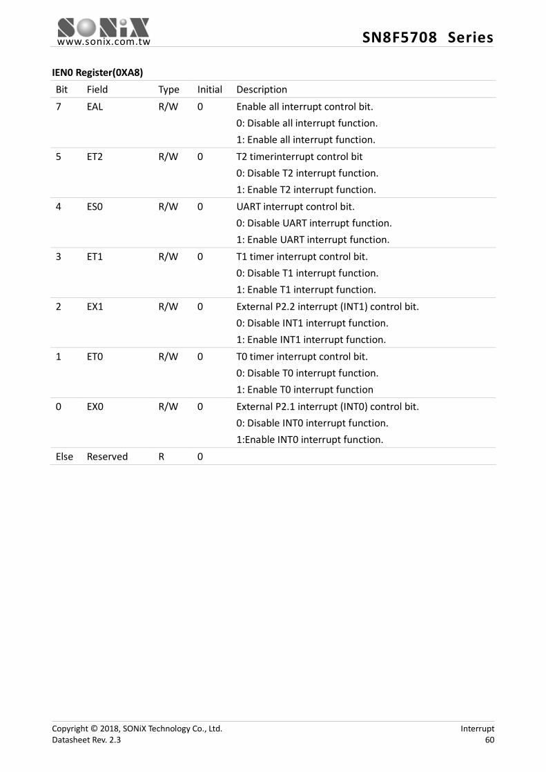
www.sonix.com.tw SN8F5708 Series
IEN0 Register(0XA8) Bit Field Type Initial Description 7 EAL R/W 0 Enable all interrupt control bit.
0: Disable all interrupt function. 1: Enable all interrupt function.
5 ET2 R/W 0 T2 timerinterrupt control bit 0: Disable T2 interrupt function. 1: Enable T2 interrupt function.
4 ES0 R/W 0 UART interrupt control bit. 0: Disable UART interrupt function. 1: Enable UART interrupt function.
3 ET1 R/W 0 T1 timer interrupt control bit. 0: Disable T1 interrupt function. 1: Enable T1 interrupt function.
2 EX1 R/W 0 External P2.2 interrupt (INT1) control bit. 0: Disable INT1 interrupt function. 1: Enable INT1 interrupt function.
1 ET0 R/W 0 T0 timer interrupt control bit. 0: Disable T0 interrupt function. 1: Enable T0 interrupt function
0 EX0 R/W 0 External P2.1 interrupt (INT0) control bit. 0: Disable INT0 interrupt function. 1:Enable INT0 interrupt function.
Else Reserved R 0
Copyright © 2018, SONiX Technology Co., Ltd. Interrupt Datasheet Rev. 2.3 60
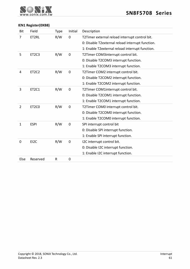
www.sonix.com.tw SN8F5708 Series
IEN1 Register(0XB8) Bit Field Type Initial Description 7 ET2RL R/W 0 T2Timer external reload interrupt control bit.
0: Disable T2external reload interrupt function. 1: Enable T2external reload interrupt function.
5 ET2C3 R/W 0 T2Timer COM3interrupt control bit. 0: Disable T2COM3 interrupt function. 1: Enable T2COM3 interrupt function.
4 ET2C2 R/W 0 T2Timer COM2 interrupt control bit. 0: Disable T2COM2 interrupt function. 1: Enable T2COM2 interrupt function.
3 ET2C1 R/W 0 T2Timer COM1interrupt control bit. 0: Disable T2COM1 interrupt function. 1: Enable T2COM1 interrupt function.
2 ET2C0 R/W 0 T2Timer COM0 interrupt control bit. 0: Disable T2COM0 interrupt function. 1: Enable T2COM0 interrupt function.
1 ESPI R/W 0 SPI interrupt control bit 0: Disable SPI interrupt function. 1: Enable SPI interrupt function.
0 EI2C R/W 0 I2C interrupt control bit. 0: Disable I2C interrupt function. 1: Enable I2C interrupt function.
Else Reserved R 0
Copyright © 2018, SONiX Technology Co., Ltd. Interrupt Datasheet Rev. 2.3 61
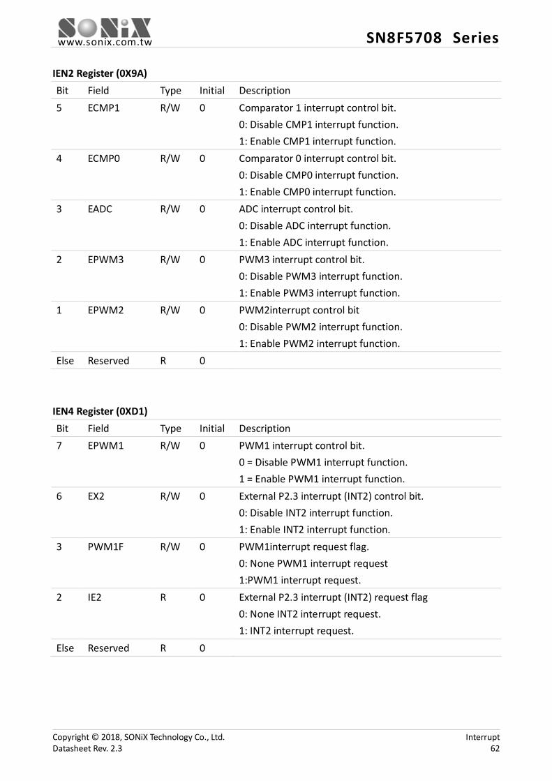
www.sonix.com.tw SN8F5708 Series
IEN2 Register (0X9A) Bit Field Type Initial Description 5 ECMP1 R/W 0 Comparator 1 interrupt control bit.
0: Disable CMP1 interrupt function. 1: Enable CMP1 interrupt function.
4 ECMP0 R/W 0 Comparator 0 interrupt control bit. 0: Disable CMP0 interrupt function. 1: Enable CMP0 interrupt function.
3 EADC R/W 0 ADC interrupt control bit. 0: Disable ADC interrupt function. 1: Enable ADC interrupt function.
2 EPWM3 R/W 0 PWM3 interrupt control bit. 0: Disable PWM3 interrupt function. 1: Enable PWM3 interrupt function.
1 EPWM2 R/W 0 PWM2interrupt control bit 0: Disable PWM2 interrupt function. 1: Enable PWM2 interrupt function.
Else Reserved R 0 IEN4 Register (0XD1) Bit Field Type Initial Description 7 EPWM1 R/W 0 PWM1 interrupt control bit.
0 = Disable PWM1 interrupt function. 1 = Enable PWM1 interrupt function.
6 EX2 R/W 0 External P2.3 interrupt (INT2) control bit. 0: Disable INT2 interrupt function. 1: Enable INT2 interrupt function.
3 PWM1F R/W 0 PWM1interrupt request flag. 0: None PWM1 interrupt request 1:PWM1 interrupt request.
2 IE2 R 0 External P2.3 interrupt (INT2) request flag 0: None INT2 interrupt request. 1: INT2 interrupt request.
Else Reserved R 0
Copyright © 2018, SONiX Technology Co., Ltd. Interrupt Datasheet Rev. 2.3 62
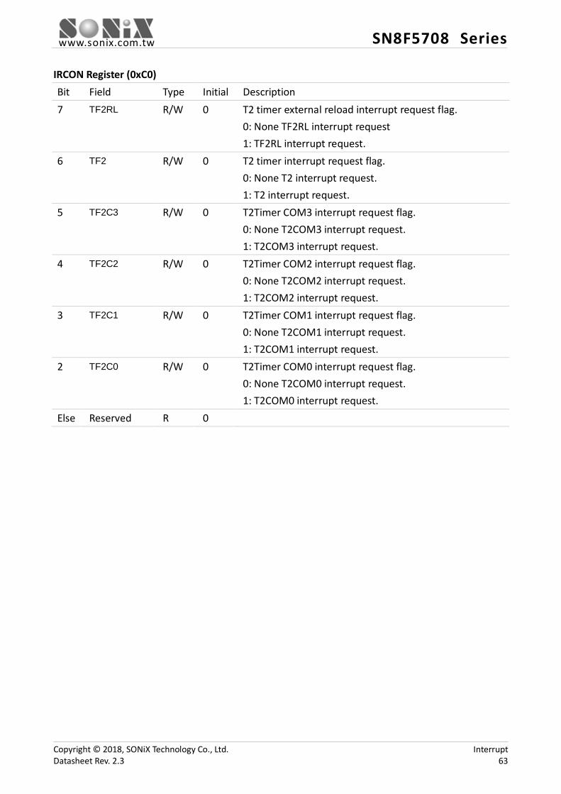
www.sonix.com.tw SN8F5708 Series
IRCON Register (0xC0) Bit Field Type Initial Description 7 TF2RL R/W 0 T2 timer external reload interrupt request flag.
0: None TF2RL interrupt request 1: TF2RL interrupt request.
6 TF2 R/W 0 T2 timer interrupt request flag. 0: None T2 interrupt request. 1: T2 interrupt request.
5 TF2C3 R/W 0 T2Timer COM3 interrupt request flag. 0: None T2COM3 interrupt request. 1: T2COM3 interrupt request.
4 TF2C2 R/W 0 T2Timer COM2 interrupt request flag. 0: None T2COM2 interrupt request. 1: T2COM2 interrupt request.
3 TF2C1 R/W 0 T2Timer COM1 interrupt request flag. 0: None T2COM1 interrupt request. 1: T2COM1 interrupt request.
2 TF2C0 R/W 0 T2Timer COM0 interrupt request flag. 0: None T2COM0 interrupt request. 1: T2COM0 interrupt request.
Else Reserved R 0
Copyright © 2018, SONiX Technology Co., Ltd. Interrupt Datasheet Rev. 2.3 63

www.sonix.com.tw SN8F5708 Series
IRCON2 Register (0XBF) Bit Field Type Initial Description 4 CMP1F R/W 0 Comparator 1 interrupt request flag.
0: None CMP1 interrupt request 1: CMP1 interrupt request
3 CMP0F R/W 0 Comparator 0 interrupt request flag. 0: None CMP0 interrupt request. 1: CMP0 interrupt request.
2 ADCF R/W 0 ADC interrupt request flag. 0: None ADC interrupt request. 1:ADC interrupt request.
1 PWM3F R/W 0 PWM3interrupt request flag. 0: None PWM3 interrupt request 1:PWM3 interrupt request.
0 PWM2F R/W 0 PWM2interrupt request flag. 0: None PWM2 interrupt request 1:PWM2 interrupt request.
Else Reserved R 0 TCON Register (0X88) Bit Field Type Initial Description 7 TF1 R/W 0 T1 timer external reload interrupt request flag.
0: None T1 interrupt request 1:T1 interrupt request.
5 TF0 R/W 0 T0 timer external reload interrupt request flag. 0: None T0 interrupt request 1:T0 interrupt request.
3 IE1 R 0 External P2.2 interrupt (INT1) request flag 0: None INT1 interrupt request. 1: INT1 interrupt request.
1 IE0 R 0 External P2.1 interrupt (INT0) request flag 0: None INT0 interrupt request. 1: INT0 interrupt request.
Else Refer to other chapter(s)
Copyright © 2018, SONiX Technology Co., Ltd. Interrupt Datasheet Rev. 2.3 64

www.sonix.com.tw SN8F5708 Series
S0CON Register(0X98) Bit Field Type Initial Description 1 TI0 R/W 0 UART transmit interrupt request flag.It indicates
completion of a serial transmission at UART. It is set by hardware at the end of bit 8 in mode 0 or at the beginning of a stop bit in other modes. It must be cleared by software. 0: None UART transmit interrupt request. 1:UART transmit interrupt request.
0 RI0 R/W 0 UART receive interrupt request flag.It is set by hardware aftercompletion of a serial reception at UART. It is set by hardware at the end of bit 8 in mode 0 or in the middle of a stop bit in other modes. It must be cleared by software. 0: None UART receive interrupt request. 1: UART receive interrupt request.
Else Refer to other chapter(s) SPSTA Register (0XE1) Bit Field Type Initial Description 7 SPIF R 0 SPI complete communication flag
Set automatically at the end of communication Cleared automatically by reading SPSTA, SPDAT registers
4 MODF R 0 Mode fault flag Else Refer to other chapter(s)
I2CCON Register(0XDC) Bit Field Type Initial Description 7 SI R/W 0 Serial interrupt flag
The SI is set by hardware when one of 25 out of 26 possible I2C states is entered. The only state that does not set the SI is state F8h, which indicates that no relevant state information is available. The SI flag must be cleared by software. In order to clear the SI bit, ‘0’ must be written to this bit. Writing a ‘1’ to SI bit does not change value of the SI.
Else Refer to other chapter(s)
Copyright © 2018, SONiX Technology Co., Ltd. Interrupt Datasheet Rev. 2.3 65

www.sonix.com.tw SN8F5708 Series
10.4 Example
Defining Interrupt Vector. The interrupt service routine is following user assembly code program. ORG 0 ; 0000H JMP START ; Jump to user program address. … ORG 0X000B ; Jump to interrupt service routine address. JMP ISR_T0 ORG 0X0013 JMP ISR_INT1 … ORG 0X009B JMP ISR_ADC … ORG 0X00EC START: ; 00ECH, The head of user program. … ; User program. … JMP START ; End of user program. … ISR_T0: ; The head of interrupt service routine. PUSH ACC ; Save ACC to stack buffer. PUSH PSW ; Save PSW to stack buffer. … POP PSW ; Load PSW from stack buffer. POP ACC ; Load ACC from stack buffer. RETI ; End of interrupt service routine. ISR_ADC: ; PUSH ACC ; Save ACC to stack buffer. PUSH PSW ; Save PSW to stack buffer. … POP PSW ; Load PSW from stack buffer. POP ACC ; Load ACC from stack buffer. RETI ; End of interrupt service routine. … ISR_INT1 ; PUSH ACC ; Save ACC to stack buffer. PUSH PSW ; Save PSW to stack buffer. … POP PSW ; Load PSW from stack buffer. POP ACC ; Load ACC from stack buffer. RETI ; End of interrupt service routine. END ; End of program.
Copyright © 2018, SONiX Technology Co., Ltd. Interrupt Datasheet Rev. 2.3 66
www.sonix.com.tw SN8F5708 Series
11 MDU
The multiplication division unit is an on-chip arithmetic co-processor which enables the microcontroller to perform additional extended arithmetic operations. This unit provides 32-bit unsigned division, 16-bit unsigned multiplication, shift and normalize operations. These operations are identified by the different sequences of writing MD0 to MD5 registers.
11.1 Multiplication (16-bit x 16-bit)
The elements of a multiplication include three parts: multiplicand, multiplier and product. To start a multiplication requires following writing sequence: MD0 (low byte of multiplicand), MD4 (low byte of multiplier), MD1 (high byte of multiplicand), and MD5 (high byte of multiplier).
By the end of writing MD5 register, the multiplication is automatically started and takes 11 CPU cycles for its operation. The product of this term operation would be available to read by a specific sequence: MD0 (LSB), MD1, MD2, and MD3 (MSB) registers.
11.2 Division (32-bit/16-bit and 16-bit/16-bit)
The MDU supports two kind of division: 32-bit by 16-bit, and 16-bit by 16-bit. The first operation takes 17 CPU cycles to compute, whereas the second one takes 9 cycles only.
A 32-bit division started by a specific sequence of writing registers: MD0, MD1, MD2, MD3, MD4, and MD5. In this case, the 32-bit dividend is expected to store in MD3 (most significant bit) to MD0 registers, and 16-bit divisor is stored in MD5 and MD4 registers (MSB in MD5 register).
A 16-bit division operation cooperates with four registers only. The 16-bit dividend is stored in MD1 and MD0 registers, and the 16-bit divisor is stored in MD5 and MD4 registers (MD1 and MD5 for most signification bit). The appropriate performing sequence is ‘MD0, MD1, MD4, and MD5.’
The MDU starts computing from MD5 register is written. It spends 9 or 17 CPU cycles, depends on the length of dividend, before the outcome is generated. The quotient is stored in MD3 to MD0 registers for 32-bit division, and MD1 to MD0 registers for 16-bit division (LSB in MD0 register). The reminder would be placed in MD5 (MSB) and MD4 registers no matter which division is performed. However, reading MD5 register must be the last operation to indicate the full division is completed.
11.3 Shifting and Normalizing
The shifting and normalizing operations rotate the 32-bit registers (MD3 to MD0, MSB in MD3) for a certain or uncertain time.
In shift operation, the 32-bit unsigned integer is shifted left or right by a specified number of bits. The direction and shifting number is specified in ARCON register. A shift operation takes 3 to 18
Copyright © 2018, SONiX Technology Co., Ltd. MDU Datasheet Rev. 2.3 67
www.sonix.com.tw SN8F5708 Series
CPU cycles depends on the shift time.
In normalizing operation, the 32-bit unsigned integer would be shifted left repeatedly until the most significant bit (7thbit of MD3 register) is 1. A normalizing operation takes 4 to 19 CPU cycles depends on the actual shift time.
Both shifting and normalizing operations are started by proper sequence of writing registers: MD0, MD1, MD2, MD3, and finally ARCON register. The result would be place in MD0 to MD3 registers which should be read in the sequence of MD0, MD1, MD2, and MD3.
11.4 Cooperate with Keil C51
Because Keil C51 supports both of hardware and software multiplication/division operators, a command line ‘#pragma mdu_r515’ is required in C to enable the hardware MDU functionality for higher performance. Subsequently, Keil C51 would compile mathematic operators with MDU support.
1 2
#include<SN8F5708.H> #pragma mdu_r515 //Keil C51 MDU command line
11.5 The Error Flag (MDEF)
The “MDEF” error flag indicates an improperly performed operation (when one of the arithmetic operations has been restarted or interrupted by a new operation). The error flag mechanism is automatically enabled with the first write operation to “MD0” and disabled with the final read instruction from “MD3” (multiplication or shift/normalize) or “MD5” (division) in phase three.
The error flag is set when: There is a write access to‘MDx’ registers (any of ’MD0’ to ‘MD5’andARCON) during phase two of MDU operation (restart or calculations interrupting) There is a read access to one ofMDxregisters during phase two of MDU operation when the error flag mechanism is enabled. In such condition error flag is set but the calculation is not interrupted. The error flag is reset only after read access to “ARCON” register. The error flag is read only.
11.6 The Overflow Flag (MDOV)
The MDOVoverflow flag is set when one of the following conditions occurs:
Division by zero Multiplication with a result greater than 0000 FFFFh Start of normalizing if the most significant bit of MD3 is set (MD3.7= 1) Any operation of the MDU that does not match the above conditions clears the overflow flag. Note that the overflow flag is exclusively controlled by hardware. It cannot be written.
Copyright © 2018, SONiX Technology Co., Ltd. MDU Datasheet Rev. 2.3 68

www.sonix.com.tw SN8F5708 Series
11.7 MDU Registers
Register Bit 7 Bit 6 Bit 5 Bit 4 Bit 3 Bit 2 Bit 1 Bit 0
MD0 MD07 MD06 MD05 MD04 MD03 MD02 MD01 MD00 MD1 MD17 MD16 MD15 MD14 MD13 MD12 MD11 MD10 MD2 MD27 MD26 MD25 MD24 MD23 MD22 MD21 MD20 MD3 MD37 MD36 MD35 MD34 MD33 MD32 MD31 MD30 MD4 MD47 MD46 MD45 MD44 MD43 MD42 MD41 MD40 MD5 MD57 MD56 MD55 MD54 MD53 MD52 MD51 MD50
ARCON MDEF MDOV SLR SC4 SC3 SC2 SC1 SC0 MD Registers (MD0 – MD5: 0xE9 – 0xEE) Bit Field Type Initial Description 7..0 MD[7:0] R/W 0x00 Multiplication/Division Registers
ARCON Register (0xEF) Bit Field Type Initial Description 7 MDEF R/W 0 MDU error flag MDEF
Indicates an improperly performed operation (when one of the arithmetic operations has been restarted or interrupted by a new operation).
6 MDOV R/W 0 MDU overflow flag Overflow occurrence in the MDU operation.
5 SLR R/W 0 Shift direction 0: Shift left operation 1: Shift right operation
4..0 SC[4:0] R/W 0x00 Shift counter Write 0x00: Perform normalizing. The actual shift time would be readable after operation. Write else values: Specify the times of shift operation.
Copyright © 2018, SONiX Technology Co., Ltd. MDU Datasheet Rev. 2.3 69

www.sonix.com.tw SN8F5708 Series
11.8 Sample Code
The following sample code demonstrates how to perform MDU 32 bit / 16 bit.
1 2 3 4 5 6 7 8 9 10 11 12 13 14 15 16 17 18
#include<SN8F5708.H> #pragma mdu_r515//Keil C51 MDU command line void main(void) { unsigned int Divisor;// 16-bit divisor unsigned long Dividend;// 32-bit dividend unsigned long Quotient;// 32-bit Quotient unsigned int Remainder;// 16-bit Remainder
Divisor= 0x1234; Dividend= 0x56789ABC; Quotient= Dividend/Divisor;//0x0004C016 Remainder = Dividend%Divisor;//0x0A44
while(1);
}
Copyright © 2018, SONiX Technology Co., Ltd. MDU Datasheet Rev. 2.3 70
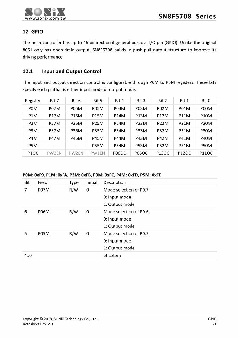
www.sonix.com.tw SN8F5708 Series
12 GPIO
The microcontroller has up to 46 bidirectional general purpose I/O pin (GPIO). Unlike the original 8051 only has open-drain output, SN8F5708 builds in push-pull output structure to improve its driving performance.
12.1 Input and Output Control
The input and output direction control is configurable through P0M to P5M registers. These bits specify each pinthat is either input mode or output mode.
Register Bit 7 Bit 6 Bit 5 Bit 4 Bit 3 Bit 2 Bit 1 Bit 0
P0M P07M P06M P05M P04M P03M P02M P01M P00M P1M P17M P16M P15M P14M P13M P12M P11M P10M P2M P27M P26M P25M P24M P23M P22M P21M P20M P3M P37M P36M P35M P34M P33M P32M P31M P30M P4M P47M P46M P45M P44M P43M P42M P41M P40M P5M - - P55M P54M P53M P52M P51M P50M P1OC PW3EN PW2EN PW1EN P06OC P05OC P13OC P12OC P11OC
P0M: 0xF9, P1M: 0xFA, P2M: 0xFB, P3M: 0xFC, P4M: 0xFD, P5M: 0xFE Bit Field Type Initial Description 7 P07M R/W 0 Mode selection of P0.7
0: Input mode 1: Output mode
6 P06M R/W 0 Mode selection of P0.6 0: Input mode 1: Output mode
5 P05M R/W 0 Mode selection of P0.5 0: Input mode 1: Output mode
4..0 et cetera
Copyright © 2018, SONiX Technology Co., Ltd. GPIO Datasheet Rev. 2.3 71
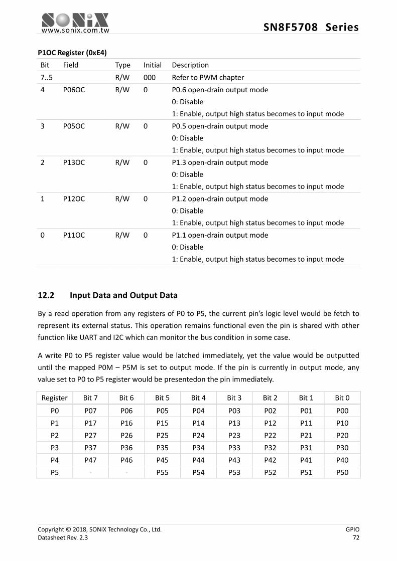
www.sonix.com.tw SN8F5708 Series
P1OC Register (0xE4) Bit Field Type Initial Description 7..5 R/W 000 Refer to PWM chapter 4 P06OC R/W 0 P0.6 open-drain output mode
0: Disable 1: Enable, output high status becomes to input mode
3 P05OC R/W 0 P0.5 open-drain output mode 0: Disable 1: Enable, output high status becomes to input mode
2 P13OC R/W 0 P1.3 open-drain output mode 0: Disable 1: Enable, output high status becomes to input mode
1 P12OC R/W 0 P1.2 open-drain output mode 0: Disable 1: Enable, output high status becomes to input mode
0 P11OC R/W 0 P1.1 open-drain output mode 0: Disable 1: Enable, output high status becomes to input mode
12.2 Input Data and Output Data
By a read operation from any registers of P0 to P5, the current pin’s logic level would be fetch to represent its external status. This operation remains functional even the pin is shared with other function like UART and I2C which can monitor the bus condition in some case.
A write P0 to P5 register value would be latched immediately, yet the value would be outputted until the mapped P0M – P5M is set to output mode. If the pin is currently in output mode, any value set to P0 to P5 register would be presentedon the pin immediately.
Register Bit 7 Bit 6 Bit 5 Bit 4 Bit 3 Bit 2 Bit 1 Bit 0
P0 P07 P06 P05 P04 P03 P02 P01 P00 P1 P17 P16 P15 P14 P13 P12 P11 P10 P2 P27 P26 P25 P24 P23 P22 P21 P20 P3 P37 P36 P35 P34 P33 P32 P31 P30 P4 P47 P46 P45 P44 P43 P42 P41 P40 P5 - - P55 P54 P53 P52 P51 P50
Copyright © 2018, SONiX Technology Co., Ltd. GPIO Datasheet Rev. 2.3 72
www.sonix.com.tw SN8F5708 Series
P0: 0x80, P1: 0x90, P2: 0xA0, P3: 0xFC, P4: 0xE8, P5: 0xF8 Bit Field Type Initial Description 7 P07 R/W 1 Read: P0.7 pin’s logic level
Write 1/0: Output logic high or low (applied if P07M = 1) 6 P06 R/W 1 Read: P0.6 pin’s logic level
Write 1/0: Output logic high or low (applied if P06M = 1) 5 P05 R/W 1 Read: P0.5 pin’s logic level
Write 1/0: Output logic high or low (applied if P05M = 1) 4..0 et cetera
12.3 On-chip Pull-up Resisters
The P0UR to P5UR registers are mapped to each pins’ internal 100 kΩ (in typical value) pull-up resister.
Register Bit 7 Bit 6 Bit 5 Bit 4 Bit 3 Bit 2 Bit 1 Bit 0
P0UR P07UR P06UR P05UR P04UR P03UR P02UR P01UR P00UR P1UR P17UR P16UR P15UR P14UR P13UR P12UR P11UR P10UR P2UR P27UR P26UR P25UR P24UR P23UR P22UR P21UR P20UR P3UR P37UR P36UR P35UR P34UR P33UR P32UR P31UR P30UR P4UR P47UR P46UR P45UR P44UR P43UR P42UR P41UR P40UR P5UR - - P55UR P54UR P53UR P52UR P51UR P50UR
P0UR: 0xF1, P1UR: 0xF2, P2UR: 0xF3, P3UR: 0xF4, P4UR: 0xF5, P5UR: 0xF6 Bit Field Type Initial Description 7 P07UR R/W 0 On-chip pull-up resister control of P0.7
0: Disable*
1: Enable 6 P06UR R/W 0 On-chip pull-up resister control of P0.6
0: Disable*
1: Enable 5 P05UR R/W 0 On-chip pull-up resister control of P0.5
0: Disable*
1: Enable 4..0 et cetera
* Recommended disable pull-up resister if the pin is output mode or analog function
Copyright © 2018, SONiX Technology Co., Ltd. GPIO Datasheet Rev. 2.3 73
www.sonix.com.tw SN8F5708 Series
12.4 Pin Shared with Analog Function
The microcontroller builds in analog functions, such as ADC, OPA and comparator.The Schmitt trigger of input channel is strongly recommended to switch off if the pin’s shared analog function is enabled.
Register Bit 7 Bit 6 Bit 5 Bit 4 Bit 3 Bit 2 Bit 1 Bit 0
P2CON P2CON7 P2CON6 P2CON5 P2CON4 - - - - P3CON P3CON7 P3CON6 P3CON5 P3CON4 P3CON3 P3CON2 P3CON1 P3CON0 P4CON P4CON7 P4CON6 P4CON5 P4CON4 P4CON3 P4CON2 P4CON1 P4CON0 P5CON - - P5CON5 P5CON4 P5CON3 P5CON2 P5CON1 P5CON0
P2CON: 0x9E, P3CON: 0x9F, P4CON: 0xD6, P5CON: 0xD7 Bit Field Type Initial Description 7 P2CON7 R/W 0 Schmitt trigger control of P2.7
0: Enable 1: Disable
6 P2CON6 R/W 0 Schmitt trigger control of P2.6 0: Enable 1: Disable
5 P2CON5 R/W 0 Schmitt trigger control of P2.5 0: Enable 1: Disable
4..0 et cetera
Copyright © 2018, SONiX Technology Co., Ltd. GPIO Datasheet Rev. 2.3 74

www.sonix.com.tw SN8F5708 Series
13 External Interrupt
INT0, INT1 and INT2 are external interrupt trigger sources. Build in edge trigger configuration function and edge direction is selected by PEDGE register. When both external interrupt (EX0/EX1/EX2) and global interrupt (EAL) are enabled, the external interrupt request flag (IE0/IE1/IE2) will be set to “1” as edge trigger event occurs. The program counter will jump to the interrupt vector (ORG 0x0003/0x0013/0x00EB) and execute interrupt service routine. Interrupt request flag will be cleared by hardware before ISR is executed.
13.1 External Interrupt Registers
Register Bit 7 Bit 6 Bit 5 Bit 4 Bit 3 Bit 2 Bit 1 Bit 0
PEDGE - - EX2G1 EX2G0 EX1G1 EX1G0 EX0G1 EX0G0
IEN0 EAL - ET2 ES0 ET1 EX1 ET0 EX0 TCON TF1 TR1 TF0 TR0 IE1 - IE0 - IEN4 EPWM1 EX2 - - PWM1F IE2 - -
PEDGE Register(0x8F) Bit Field Type Initial Description 5..4 EX2G[1:0] R/W 10 External interrupt 2 trigger edge control register.
00: Reserved. 01: Rising edge trigger. 10: Falling edge trigger (default) 11: Both rising and falling edge trigger
3..2 EX1G[1:0] R/W 10 External interrupt 1 trigger edge control register. 00: Reserved. 01: Rising edge trigger. 10: Falling edge trigger (default) 11: Both rising and falling edge trigger
1..0 EX0G[1:0] R/W 10 External interrupt 0 trigger edge control register. 00: Reserved. 01: Rising edge trigger. 10: Falling edge trigger (default) 11: Both rising and falling edge trigger
Else Reserved R 0
Copyright © 2018, SONiX Technology Co., Ltd. External Interrupt Datasheet Rev. 2.3 75
www.sonix.com.tw SN8F5708 Series
IEN0 Register(0xA8) Bit Field Type Initial Description 7 EAL R/W 0 Enable all interrupt control bit.
0: Disable all interrupt function. 1: Enable all interrupt function.
2 EX1 R/W 0 External P2.2 interrupt (INT1) control bit. 0: Disable INT1 interrupt function. 1: Enable INT1 interrupt function.
0 EX0 R/W 0 External P2.1 interrupt (INT0) control bit. 0: Disable INT0 interrupt function. 1:Enable INT0 interrupt function.
Else Refer to other chapter(s)
TCON Register (0x88) Bit Field Type Initial Description 3 IE1 R/W 0 External P2.2 interrupt (INT1) request flag
0: None INT1 interrupt request. 1: INT1 interrupt request.
1 IE0 R/W 0 External P2.1 interrupt (INT0) request flag 0: None INT0 interrupt request. 1: INT0 interrupt request.
Else Refer to other chapter(s)
IEN4 Register(0xD1) Bit Field Type Initial Description 6 EX2 R/W 0 External P2.3 interrupt (INT2) control bit.
0: Disable INT2 interrupt function. 1: Enable INT2 interrupt function.
0 IE2 R/W 0 External P2.3 interrupt (INT2) request flag 0: None INT2 interrupt request. 1: INT2 interrupt request.
Else Refer to other chapter(s)
Note: Before clear one of TF0, TF1, IE0 or IE1 flag manually by firmware, user must be made sure others request flag in TCON register doesn’t active.
Copyright © 2018, SONiX Technology Co., Ltd. External Interrupt Datasheet Rev. 2.3 76

www.sonix.com.tw SN8F5708 Series
13.2 Sample Code
The following sample code demonstrates how to perform INT0/INT1/INT2 with interrupt.
1 2 3 4 5 6 7 8 9 10 11 12 13 14 15 16 17 18 19 20 21 22 23 24 25 26 27 28 29 30 31 32 33 34 35 36 37 38 39 40 41 42 43 44 45
#define INT0Rsing (1<< 0) //INT0 trigger edge is rising edge #define INT0Falling (2<< 0) //INT0 trigger edge is falling edge #define INT0LeChge (3 << 0) //INT0 trigger edge is level chagne #define EINT0 (1<<0) //INT0 interrupt enable #define INT1Rsing (1<<2) //INT1 trigger edge is rising edge #define INT1Falling (2<<2) //INT1 trigger edge is falling edge #define INT1LeChge (3 <<2) //INT1 trigger edge is level chagne #define EINT1 (1<<2) //INT1 interrupt enable #define INT2Rsing (1<<4) //INT2 trigger edge is rising edge #define INT2Falling (2<<4) //INT2 trigger edge is falling edge #define INT2LeChge (3 <<4) //INT2 trigger edge is level chagne #define EINT2 (1<<6) //INT2 interrupt enable void EnableINT(void) { // INT0 rising edge, INT1 falling edge, INT2 level change PEDGE = INT0Rising |INT1Falling | INT2LeChge; // Enable INT0/INT1 interrupt IEN0|= EINT0 | EINT1; // Enable INT2 interrupt IEN4|= EINT2; // Enable total interrupt IEN0 |= 0x80; P0 = 0x00; P0M = 0x07;
} void INT0Interrupt(void) interrupt ISRInt0 //0x03 { //IE0 clear by hardware P00 = ~P00;
} void INT1Interrupt(void) interrupt ISRInt1 //0x13 { //IE1 clear by hardware P01 = ~P01;
} void INT2Interrupt(void) interrupt ISRInt2 //0xEB { //IE2 clear by hardware P02 = ~P02;
}
Copyright © 2018, SONiX Technology Co., Ltd. External Interrupt Datasheet Rev. 2.3 77

www.sonix.com.tw SN8F5708 Series
14 Timer 0 and Timer 1
Timer 0 and Timer 1 are two independent binary up timers. Timer 0 has four different operation modes: (1) 13-bit up counting timer, (2) 16-bit up counting timer, (3) 8-bit up counting timer with specified reload value support, and (4) separated two 8-bit up counting timer. By contrast, Timer 1 has only mode 0 to mode 2 which are same as Timer 0. Timer 0 and Timer 1 respectively support ET0 and ET1 interrupt function.
14.1 Timer 0 and Timer 1 Clock Selection
The figures below illustrate the clock selection circuit of Timer 0 and Timer 1. Timer 0 has three clock sources selection: fcpu, fosc, and f RTC. All clock sources can be gated (pause) by INT0 pin if T0GATE is applied. Timer 1 clock sources selection: fcpu and fosc. All clock sources can be gated (pause) by INT1 pin if T1GATE is applied. Overall, the major difference between the two timers is that Timer 0 additionally supports f RTC clock source (real time counter, RTC) which is functional if the microcontroller’s CPU clock is ‘IHRC 32 MHz with RTC’(refer to Reset and Power-on Controller) and an off-chip 32 kHz crystal is connected.
÷12
MUX
fcpu
fosc
fRTC
T0EXT
MUX
T0CT T0GATE
INT0
Timer 0 clock
T0RATE
Divider÷1 to ÷128
MUX
÷12fcpu
fosc
MUX
T1CT T1GATE
INT1
Timer 1 clock
T1RATE
Divider÷1 to ÷128
MUX
Copyright © 2018, SONiX Technology Co., Ltd. Timer 0 and Timer 1 Datasheet Rev. 2.3 78

www.sonix.com.tw SN8F5708 Series
14.2 Mode 0: 13-bit Up Counting Timer
Mode 0 is a 13-bit up counting timer (the upper 3 bits of TL0 is suspended). Once the timer’s counter is overflow (counts from 0xFF1F to 0x0000), TF0/TF1 flag would be issued immediately.This flag is readable by firmware if ET0/ET1 does not apply, or can be handled by interrupt controller if ET0/ET1 is applied.
Timer 0 clock TH0[7:0]TL0[4:0] TF0
Timer 1 clock TH1[7:0]TL1[4:0] TF1
14.3 Mode 1: 16-bit Up Counting Timer
Mode 1 is a 16-bit up counting timer.Once the timer’s counter overflow is occurred (from 0xFFFF to 0x0000), TF0/TF1 would be issued which is readable by firmware or can be handled by interrupt controller (if ET0/ET1 applied).
Timer 0 clock TH0[7:0]TL0[7:0] TF0
Timer 1 clock TH1[7:0]TL1[7:0] TF1
14.4 Mode 2: 8-bit Up Counting Timer with Specified Reload Value Support
Mode 2 is an 8-bit up counting timer (TL0/TL1) with a specifiable reload value. An overflow event (TL0/TL1 counts from 0xFF to 0x00) issues its TF0/TF1 flag for firmware or interrupt controller; meanwhile, the timer duplicates TH0/TH1 value to TL0/TL1 register in the same time. As a result, the timer is actually counts from 0xFF to the value of TH0/TH1.
Timer 0 clock TL0[7:0]
TH0[7:0]
TF0
Reload
Timer 1 clock TL1[7:0]
TH1[7:0]
TF1
Reload
Copyright © 2018, SONiX Technology Co., Ltd. Timer 0 and Timer 1 Datasheet Rev. 2.3 79
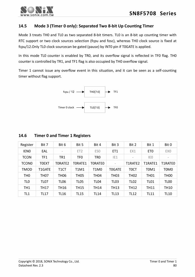
www.sonix.com.tw SN8F5708 Series
14.5 Mode 3 (Timer 0 only): Separated Two 8-bit Up Counting Timer
Mode 3 treats TH0 and TL0 as two separated 8-bit timers. TL0 is an 8-bit up counting timer with RTC support or two clock sources selection (fcpu and fosc), whereas TH0 clock source is fixed at fcpu/12.Only TL0 clock sourcecan be gated (pause) by INT0 pin if T0GATE is applied.
In this mode TL0 counter is enabled by TR0, and its overflow signal is reflected in TF0 flag. TH0 counter is controlled by TR1, and TF1 flag is also occupied by TH0 overflow signal.
Timer 1 cannot issue any overflow event in this situation, and it can be seen as a self-counting timer without flag support.
fcpu / 12 TH0[7:0] TF1
Timer 0 clock TL0[7:0] TF0
14.6 Timer 0 and Timer 1 Registers
Register Bit 7 Bit 6 Bit 5 Bit 4 Bit 3 Bit 2 Bit 1 Bit 0
IEN0 EAL - ET2 ES0 ET1 EX1 ET0 EX0 TCON TF1 TR1 TF0 TR0 IE1 - IE0 -
TCON0 T0EXT T0RATE2 T0RATE1 T0RATE0 - T1RATE2 T1RATE1 T1RATE0 TMOD T1GATE T1CT T1M1 T1M0 T0GATE T0CT T0M1 T0M0
TH0 TH07 TH06 TH05 TH04 TH03 TH02 TH01 TH00 TL0 TL07 TL06 TL05 TL04 TL03 TL02 TL01 TL00 TH1 TH17 TH16 TH15 TH14 TH13 TH12 TH11 TH10 TL1 TL17 TL16 TL15 TL14 TL13 TL12 TL11 TL10
Copyright © 2018, SONiX Technology Co., Ltd. Timer 0 and Timer 1 Datasheet Rev. 2.3 80
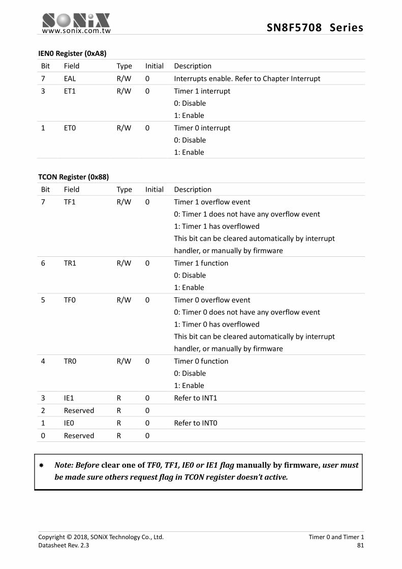
www.sonix.com.tw SN8F5708 Series
IEN0 Register (0xA8) Bit Field Type Initial Description 7 EAL R/W 0 Interrupts enable. Refer to Chapter Interrupt 3 ET1 R/W 0 Timer 1 interrupt
0: Disable 1: Enable
1 ET0 R/W 0 Timer 0 interrupt 0: Disable 1: Enable
TCON Register (0x88) Bit Field Type Initial Description 7 TF1 R/W 0 Timer 1 overflow event
0: Timer 1 does not have any overflow event 1: Timer 1 has overflowed This bit can be cleared automatically by interrupt handler, or manually by firmware
6 TR1 R/W 0 Timer 1 function 0: Disable 1: Enable
5 TF0 R/W 0 Timer 0 overflow event 0: Timer 0 does not have any overflow event 1: Timer 0 has overflowed This bit can be cleared automatically by interrupt handler, or manually by firmware
4 TR0 R/W 0 Timer 0 function 0: Disable 1: Enable
3 IE1 R 0 Refer to INT1 2 Reserved R 0 1 IE0 R 0 Refer to INT0 0 Reserved R 0
Note: Before clear one of TF0, TF1, IE0 or IE1 flag manually by firmware, user must be made sure others request flag in TCON register doesn’t active.
Copyright © 2018, SONiX Technology Co., Ltd. Timer 0 and Timer 1 Datasheet Rev. 2.3 81
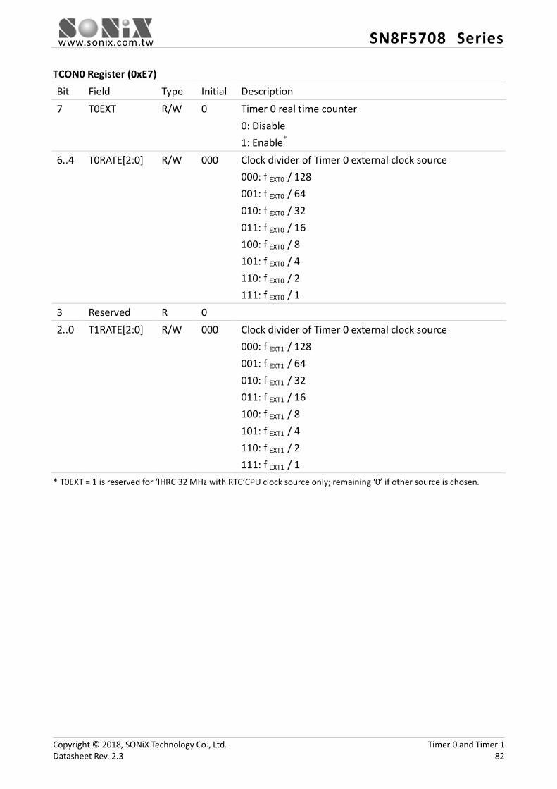
www.sonix.com.tw SN8F5708 Series
TCON0 Register (0xE7) Bit Field Type Initial Description 7 T0EXT R/W 0 Timer 0 real time counter
0: Disable 1: Enable*
6..4 T0RATE[2:0] R/W 000 Clock divider of Timer 0 external clock source 000: f EXT0 / 128 001: f EXT0 / 64 010: f EXT0 / 32 011: f EXT0 / 16 100: f EXT0 / 8 101: f EXT0 / 4 110: f EXT0 / 2 111: f EXT0 / 1
3 Reserved R 0 2..0 T1RATE[2:0] R/W 000 Clock divider of Timer 0 external clock source
000: f EXT1 / 128 001: f EXT1 / 64 010: f EXT1 / 32 011: f EXT1 / 16 100: f EXT1 / 8 101: f EXT1 / 4 110: f EXT1 / 2 111: f EXT1 / 1
* T0EXT = 1 is reserved for ‘IHRC 32 MHz with RTC’CPU clock source only; remaining ‘0’ if other source is chosen.
Copyright © 2018, SONiX Technology Co., Ltd. Timer 0 and Timer 1 Datasheet Rev. 2.3 82
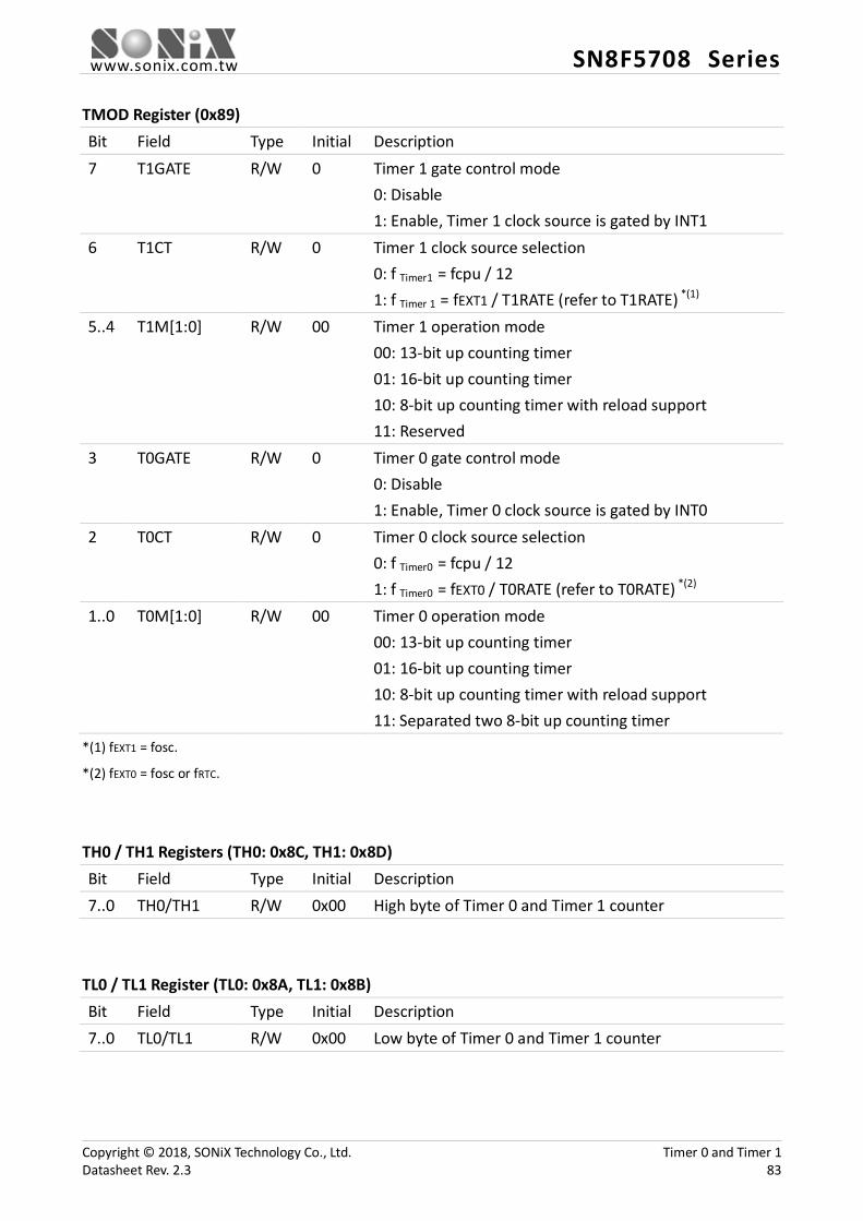
www.sonix.com.tw SN8F5708 Series
TMOD Register (0x89) Bit Field Type Initial Description 7 T1GATE R/W 0 Timer 1 gate control mode
0: Disable 1: Enable, Timer 1 clock source is gated by INT1
6 T1CT R/W 0 Timer 1 clock source selection 0: f Timer1 = fcpu / 12 1: f Timer 1 = fEXT1 / T1RATE (refer to T1RATE) *(1)
5..4 T1M[1:0] R/W 00 Timer 1 operation mode 00: 13-bit up counting timer 01: 16-bit up counting timer 10: 8-bit up counting timer with reload support 11: Reserved
3 T0GATE R/W 0 Timer 0 gate control mode 0: Disable 1: Enable, Timer 0 clock source is gated by INT0
2 T0CT R/W 0 Timer 0 clock source selection 0: f Timer0 = fcpu / 12 1: f Timer0 = fEXT0 / T0RATE (refer to T0RATE) *(2)
1..0 T0M[1:0] R/W 00 Timer 0 operation mode 00: 13-bit up counting timer 01: 16-bit up counting timer 10: 8-bit up counting timer with reload support 11: Separated two 8-bit up counting timer
*(1) fEXT1 = fosc.
*(2) fEXT0 = fosc or fRTC.
TH0 / TH1 Registers (TH0: 0x8C, TH1: 0x8D) Bit Field Type Initial Description 7..0 TH0/TH1 R/W 0x00 High byte of Timer 0 and Timer 1 counter
TL0 / TL1 Register (TL0: 0x8A, TL1: 0x8B) Bit Field Type Initial Description 7..0 TL0/TL1 R/W 0x00 Low byte of Timer 0 and Timer 1 counter
Copyright © 2018, SONiX Technology Co., Ltd. Timer 0 and Timer 1 Datasheet Rev. 2.3 83
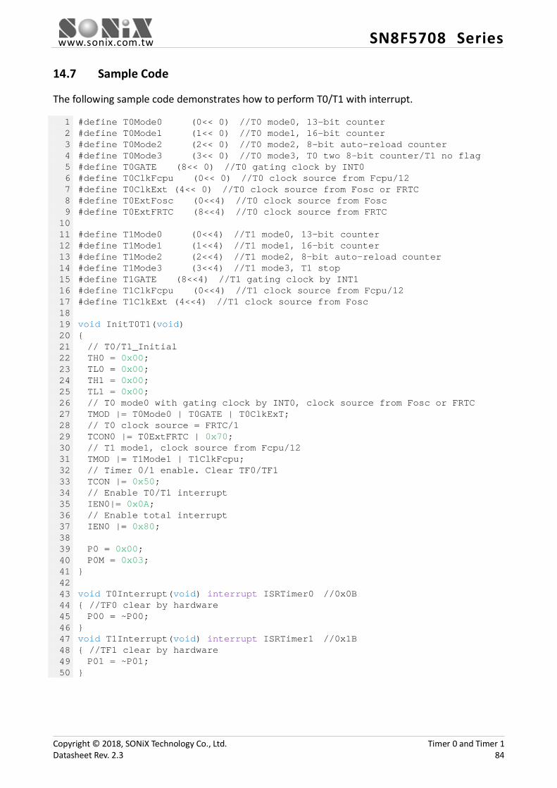
www.sonix.com.tw SN8F5708 Series
14.7 Sample Code
The following sample code demonstrates how to perform T0/T1 with interrupt.
1 2 3 4 5 6 7 8 9 10 11 12 13 14 15 16 17 18 19 20 21 22 23 24 25 26 27 28 29 30 31 32 33 34 35 36 37 38 39 40 41 42 43 44 45 46 47 48 49 50
#define T0Mode0 (0<< 0) //T0 mode0, 13-bit counter #define T0Mode1 (1<< 0) //T0 mode1, 16-bit counter #define T0Mode2 (2<< 0) //T0 mode2, 8-bit auto-reload counter #define T0Mode3 (3<< 0) //T0 mode3, T0 two 8-bit counter/T1 no flag #define T0GATE (8<< 0) //T0 gating clock by INT0 #define T0ClkFcpu (0<< 0) //T0 clock source from Fcpu/12 #define T0ClkExt (4<< 0) //T0 clock source from Fosc or FRTC #define T0ExtFosc (0<<4) //T0 clock source from Fosc #define T0ExtFRTC (8<<4) //T0 clock source from FRTC #define T1Mode0 (0<<4) //T1 mode0, 13-bit counter #define T1Mode1 (1<<4) //T1 mode1, 16-bit counter #define T1Mode2 (2<<4) //T1 mode2, 8-bit auto-reload counter #define T1Mode3 (3<<4) //T1 mode3, T1 stop #define T1GATE (8<<4) //T1 gating clock by INT1 #define T1ClkFcpu (0<<4) //T1 clock source from Fcpu/12 #define T1ClkExt (4<<4) //T1 clock source from Fosc void InitT0T1(void) { // T0/T1_Initial TH0 = 0x00; TL0 = 0x00; TH1 = 0x00; TL1 = 0x00; // T0 mode0 with gating clock by INT0, clock source from Fosc or FRTC TMOD |= T0Mode0 | T0GATE | T0ClkExT; // T0 clock source = FRTC/1 TCON0 |= T0ExtFRTC | 0x70; // T1 mode1, clock source from Fcpu/12 TMOD |= T1Mode1 | T1ClkFcpu; // Timer 0/1 enable. Clear TF0/TF1 TCON |= 0x50; // Enable T0/T1 interrupt IEN0|= 0x0A; // Enable total interrupt IEN0 |= 0x80; P0 = 0x00; P0M = 0x03;
} void T0Interrupt(void) interrupt ISRTimer0 //0x0B { //TF0 clear by hardware P00 = ~P00;
} void T1Interrupt(void) interrupt ISRTimer1 //0x1B { //TF1 clear by hardware P01 = ~P01;
}
Copyright © 2018, SONiX Technology Co., Ltd. Timer 0 and Timer 1 Datasheet Rev. 2.3 84

www.sonix.com.tw SN8F5708 Series
15 Timer 2
Timer 2 is a 16-bit up counting timer which has several optional extensions: specified reload value, comparison output (PWM) and capture function.Timer 2 consists of a dedicated 16-bit counter/timer and four 16-bit capture/compare modules. Each capture/compare module has its own associated I/O when enabled.Each capture/compare module may be configured to operateindependently in one of 3 modes: compare, capture with rising edge, or capture with register be written.
16-bit Counter/TimerTH2/TL2
Capture/comparemodule CRC
Capture/comparemodule CC1
Capture/comparemodule CC2
Capture/comparemodule CC3
T2COM0
T2COM1
T2COM2
T2COM3
T2CC0
T2CC1
T2CC2
T2CC3
Timer 2 clock
15.1 Timer 2 Up-counting Control
Timer 2 has three operation modes by its clock source: specify fcpu clocks (fcpu/12 and fcpu/24), specify fcpu clocks with a stop control, and external clock input. The table below categorizes these three operation modes and its related registers (T2I1, T2I0 and T2PS).Once the timer’s counter is overflow (counts from 0xFFFF to 0x0000), TF2 would be issued immediately which can read/write by firmware. Timer 2 interrupt function is controlled by ET2.
T2I1 T2I0 T2PS Timer 2 Clock Source
0 0 X Disable Timer 2 0 1 0 fcpu/12 0 1 1 fcpu/24 1 1 0 fcpu/12 (stop counting when T2 pin is low, resume when T2 is high) 1 1 1 fcpu/24 (stop counting when T2 pin is low, resume when T2 is high) 1 0 X T2 pin rising edge (T2 pin is shared with P2.3, clock rate ≤ 0.5 * fcpu)
Copyright © 2018, SONiX Technology Co., Ltd. Timer 2 Datasheet Rev. 2.3 85
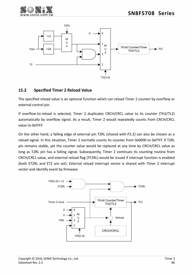
www.sonix.com.tw SN8F5708 Series
÷24fcpu
T2
MUX
T2PS
T2I[1:0]
MUX
÷120 0
1
3
2
16-bit Counter/TimerTH2/TL2 TF2
15.2 Specified Timer 2 Reload Value
The specified reload value is an optional function which can reload Timer 2 counter by overflow or external control pin.
If overflow-to-reload is selected, Timer 2 duplicates CRCH/CRCL value to its counter (TH2/TL2) automatically by overflow signal. As a result, Timer 2 would repeatedly counts from CRCH/CRCL value to 0xFFFF.
On the other hand, a falling edge of external pin T2RL (shared with P2.2) can also be chosen as a reload signal. In this situation, Timer 2 normally counts its counter from 0x0000 to 0xFFFF if T2RL pin remains stable, yet the counter value would be replaced at any time by CRCH/CRCL value as long as T2RL pin has a falling signal. Subsequently, Timer 2 continues its counting routine from CRCH/CRCL value, and external reload flag (TF2RL) would be issued if interrupt function is enabled (both ET2RL and ET2 are set). External reload interrupt vector is shared with Timer 2 interrupt vector and identify event by firmware.
16-bit Counter/TimerTH2/TL2Timer 2 clock
CRCH/CRCL
MUX
Reload
TF2
0 1
3
0 0
2
T2RL
TF2RL
T2R[1:0]
ET2RL
T2R[1:0] = 11
Copyright © 2018, SONiX Technology Co., Ltd. Timer 2 Datasheet Rev. 2.3 86
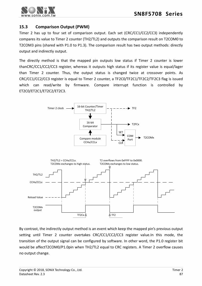
www.sonix.com.tw SN8F5708 Series
15.3 Comparison Output (PWM) Timer 2 has up to four set of comparison output. Each set (CRC/CC1/CC2/CC3) independently compares its value to Timer 2 counter (TH2/TL2) and outputs the comparison result on T2COM0 to T2COM3 pins (shared with P1.0 to P1.3). The comparison result has two output methods: directly output and indirectly output.
The directly method is that the mapped pin outputs low status if Timer 2 counter is lower thanCRC/CC1/CC2/CC3 register, whereas it outputs high status if its register value is equal/lager than Timer 2 counter. Thus, the output status is changed twice at crossover points. As CRC/CC1/CC2/CC3 register is equal to Timer 2 counter, a TF2C0/TF2C1/TF2C2/TF2C3 flag is issued which can read/write by firmware. Compare interrupt function is controlled by ET2C0/ET2C1/ET2C2/ET2C3.
16-bit Counter/TimerTH2/TL2
T2FCx
Timer 2 clock
16-bitComparator
Compare moduleCCHx/CCLx
TF2
COMPort
T2COMx
SET
CLR
TH2/TL2
CCHx/CCLx
Reload Value
T2COMxoutput
TF2Cx TF2
TH2/TL2 = CCHx/CCLx.T2COMx exchanges to high status.
T2 overflows from 0xFFFF to 0x0000. T2COMx exchanges to low status.
By contrast, the indirectly output method is an event which keep the mapped pin’s previous output setting until Timer 2 counter overtakes CRC/CC1/CC2/CC3 register value.In this mode, the transition of the output signal can be configured by software. In other word, the P1.0 register bit would be affectT2COM0/P1.0pin when TH2/TL2 equal to CRC registers. A Timer 2 overflow causes no output change.
Copyright © 2018, SONiX Technology Co., Ltd. Timer 2 Datasheet Rev. 2.3 87
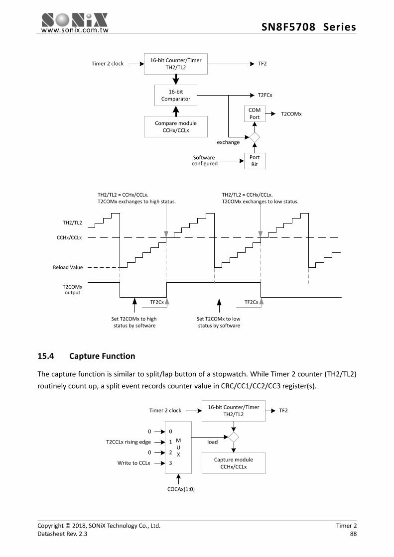
www.sonix.com.tw SN8F5708 Series
16-bit Counter/TimerTH2/TL2
T2FCx
Timer 2 clock
16-bitComparator
Compare moduleCCHx/CCLx
TF2
COMPort T2COMx
exchange
Software configured
PortBit
TH2/TL2
CCHx/CCLx
Reload Value
T2COMxoutput
TF2Cx
TH2/TL2 = CCHx/CCLx.T2COMx exchanges to high status.
TF2Cx
TH2/TL2 = CCHx/CCLx.T2COMx exchanges to low status.
Set T2COMx to high status by software
Set T2COMx to low status by software
15.4 Capture Function
The capture function is similar to split/lap button of a stopwatch. While Timer 2 counter (TH2/TL2) routinely count up, a split event records counter value in CRC/CC1/CC2/CC3 register(s).
MUX
16-bit Counter/TimerTH2/TL2
0
Timer 2 clock
Capture moduleCCHx/CCLx
TF2
0
COCAx[1:0]
load1
2
3
0
Write to CCLx
T2CCLx rising edge
Copyright © 2018, SONiX Technology Co., Ltd. Timer 2 Datasheet Rev. 2.3 88
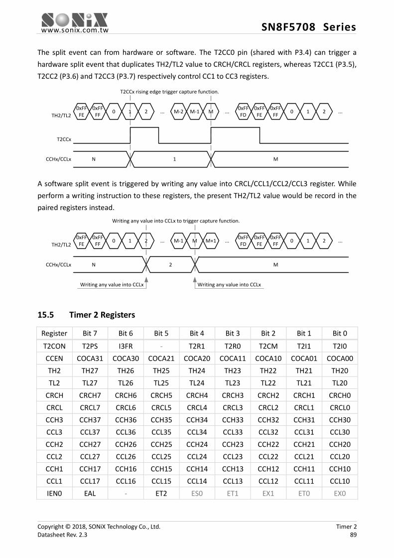
www.sonix.com.tw SN8F5708 Series
The split event can from hardware or software. The T2CC0 pin (shared with P3.4) can trigger a hardware split event that duplicates TH2/TL2 value to CRCH/CRCL registers, whereas T2CC1 (P3.5), T2CC2 (P3.6) and T2CC3 (P3.7) respectively control CC1 to CC3 registers.
0 1 2TH2/TL2
... M-2 M-1 M
T2CCx
... 0xFFFD
0xFFFE
0xFFFF 0 1 2 ...
T2CCx rising edge trigger capture function.
0xFFFE
0xFFFF
N 1 MCCHx/CCLx
A software split event is triggered by writing any value into CRCL/CCL1/CCL2/CCL3 register. While perform a writing instruction to these registers, the present TH2/TL2 value would be record in the paired registers instead.
0 1 2TH2/TL2
... M-1 M M+1 ... 0xFFFD
0xFFFE
0xFFFF 0 1 2 ...
Writing any value into CCLx to trigger capture function.
0xFFFE
0xFFFF
N 2 MCCHx/CCLx
Writing any value into CCLx Writing any value into CCLx
15.5 Timer 2 Registers
Register Bit 7 Bit 6 Bit 5 Bit 4 Bit 3 Bit 2 Bit 1 Bit 0
T2CON T2PS I3FR - T2R1 T2R0 T2CM T2I1 T2I0 CCEN COCA31 COCA30 COCA21 COCA20 COCA11 COCA10 COCA01 COCA00 TH2 TH27 TH26 TH25 TH24 TH23 TH22 TH21 TH20 TL2 TL27 TL26 TL25 TL24 TL23 TL22 TL21 TL20
CRCH CRCH7 CRCH6 CRCH5 CRCH4 CRCH3 CRCH2 CRCH1 CRCH0 CRCL CRCL7 CRCL6 CRCL5 CRCL4 CRCL3 CRCL2 CRCL1 CRCL0 CCH3 CCH37 CCH36 CCH35 CCH34 CCH33 CCH32 CCH31 CCH30 CCL3 CCL37 CCL36 CCL35 CCL34 CCL33 CCL32 CCL31 CCL30 CCH2 CCH27 CCH26 CCH25 CCH24 CCH23 CCH22 CCH21 CCH20 CCL2 CCL27 CCL26 CCL25 CCL24 CCL23 CCL22 CCL21 CCL20 CCH1 CCH17 CCH16 CCH15 CCH14 CCH13 CCH12 CCH11 CCH10 CCL1 CCL17 CCL16 CCL15 CCL14 CCL13 CCL12 CCL11 CCL10 IEN0 EAL - ET2 ES0 ET1 EX1 ET0 EX0
Copyright © 2018, SONiX Technology Co., Ltd. Timer 2 Datasheet Rev. 2.3 89
www.sonix.com.tw SN8F5708 Series
IEN1 ET2RL - ET2C3 ET2C2 ET2C1 ET2C0 ESPI EI2C IRCON TF2RL TF2 TF2C3 TF2C2 TF2C1 TF2C0 - -
T2CON Register (0xC8) Bit Field Type Initial Description 7 T2PS R/W 0 Timer 2 pre-scalar
0: fcpu/12 1: fcpu/24
6 I3FR R/W 0 In compare mode: 0: The COM0 interrupt would be generated when the
TH2/TL2 becomes not equal to the CRCregister (e.g. Timer 2: 0x8081, CRC: 0x8080).
1: The COM0 interrupt would be generated when the TH2/TL2 becomes equal to the CRC register.
In capture mode 0: 0: The timer 2 content would be latched into CRC
register by T2CC0 is falling edge. 1: The timer 2 content would be latched into CRC
register by T2CC0 is rising edge. 5 Reserved R/W 0 4..3 T2R[1:0] R/W 00 Specified Timer 2 reload value
00: Disable 01: Disable 10: Load CRCH/CRCL to TH2/TL2 by counter overflow 11: Load CRCH/CRCL to TH2/TL2 by T2RL pin
2 T2CM R/W 0 Timer 2 comparison output 0: Directly output method 1: Indirectly output, next output status can be specified
1..0 T2I[1:0] R/W 00 Timer 2 up counting control 00: Disable 01: Clock rate is defined by T2PS 10: Clock source is T2 pin 11: Clock rate is defined by T2PS with T2 pin gate control
Copyright © 2018, SONiX Technology Co., Ltd. Timer 2 Datasheet Rev. 2.3 90

www.sonix.com.tw SN8F5708 Series
CCEN Register (0xC1) Bit Field Type Initial Description 7..6 COCA3[1:0] R/W 00 Comparison and capture function of CC3
00: Disable 01: Capture by T2CC3 pin rising edge 10: Comparison function 11: Capture by writing CCL3 register
5..4 COCA2[1:0] R/W 00 Comparison and capture function of CC2 00: Disable 01: Capture by T2CC2 pin rising edge 10: Comparison function 11: Capture by writing CCL2 register
3..2 COCA1[1:0] R/W 00 Comparison and capture function of CC1 00: Disable 01: Capture by T2CC1 pin rising edge 10: Comparison function 11: Capture by writing CCL1 register
1..0 COCA0[1:0] R/W 00 Comparison and capture function of CRC 00: Disable 01: Capture by T2CC0 pin rising edge 10: Comparison function 11: Capture by writing CRCL register
TH2/TL2 Registers (TH2: 0xCD, TL2: 0xCC) Bit Field Type Initial Description 7..0 TH2/TL2 R/W 0x00 Timer 2 16-bit counter registers.
CRC Registers (CRCH: 0xCB, CRCL: 0xCA) Bit Field Type Initial Description 7..6 CRCH[15:0] R/W 0x00 16-bit compare/capture registers.
CCH3/CCL3 Registers (CCH3: 0xC7, CCL3: 0xC6) Bit Field Type Initial Description 7..6 CCH3/CCL3 R/W 0x00 16-bit compare/capture registers.
Copyright © 2018, SONiX Technology Co., Ltd. Timer 2 Datasheet Rev. 2.3 91

www.sonix.com.tw SN8F5708 Series
CCH2/CCL2 Registers (CCH2: 0xC5, CCL2: 0xC4) Bit Field Type Initial Description 7..6 CCH2 /CCL2 R/W 0x00 16-bit compare/capture registers.
CCH1/CCL1 Registers (CCH1: 0xC3, CCL1: 0xC2) Bit Field Type Initial Description 7..6 CCH1/CCL1 R/W 0x00 16-bit compare/capture registers.
IEN0 Register (0xA8) Bit Field Type Initial Description 7 EAL R/W 0 Interrupts enable. Refer to Chapter Interrupt 5 ET2 R/W 0 Enable Timer 2 interrupt Else Refer to other chapter(s)
IEN1 Register (0xB8) Bit Field Type Initial Description 7 ET2RL R/W 0 T2 Timer external reload interrupt control bit
0: Disable 1: Enable
6 Reserved R 0 5 ET2C3 R/W 0 T2 Timer COM3 interrupt control bit
0: Disable 1: Enable
4 ET2C2 R/W 0 T2 Timer COM2 interrupt control bit 0: Disable 1: Enable
3 ET2C1 R/W 0 T2 Timer COM1 interrupt control bit 0: Disable 1: Enable
2 ET2C0 R/W 0 T2 Timer COM0 interrupt control bit 0: Disable 1: Enable
Else Refer to other chapter(s)
Copyright © 2018, SONiX Technology Co., Ltd. Timer 2 Datasheet Rev. 2.3 92

www.sonix.com.tw SN8F5708 Series
IRCON Register (0xC0) Bit Field Type Initial Description 7 TF2RL R/W 0 T2 timer external reload interrupt request flag.
0: None TF2RL interrupt request 1: TF2RL interrupt request.
6 TF2 R/W 0 T2 timer interrupt request flag. 0: None T2 interrupt request. 1: T2 interrupt request.
5 TF2C3 R/W 0 T2Timer COM3 interrupt request flag. 0: None T2COM3 interrupt request. 1: T2COM3 interrupt request.
4 TF2C2 R/W 0 T2Timer COM2 interrupt request flag. 0: None T2COM2 interrupt request. 1: T2COM2 interrupt request.
3 TF2C1 R/W 0 T2Timer COM1 interrupt request flag. 0: None T2COM1 interrupt request. 1: T2COM1 interrupt request.
2 TF2C0 R/W 0 T2Timer COM0 interrupt request flag. 0: None T2COM0 interrupt request. 1: T2COM0 interrupt request.
Else Reserved R 0
Copyright © 2018, SONiX Technology Co., Ltd. Timer 2 Datasheet Rev. 2.3 93
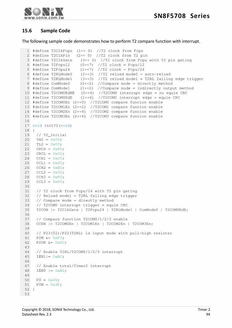
www.sonix.com.tw SN8F5708 Series
15.6 Sample Code
The following sample code demonstrates how to perform T2 compare function with interrupt.
1 2 3 4 5 6 7 8 9 10 11 12 13 14 15 16 17 18 19 20 21 22 23 24 25 26 27 28 29 30 31 32 33 34 35 36 37 38 39 40 41 42 43 44 45 46 47 48 49 50 51 52 53
#define T2ClkFcpu (1<< 0) //T2 clock from Fcpu #define T2ClkPin (2<< 0) //T2 clock from T2 pin #define T2ClkGate (3<< 0) //T2 clock from Fcpu with T2 pin gating #define T2Fcpu12 (0<<7) //T2 clock = Fcpu/12 #define T2Fcpu24 (1<<7) //T2 clock = Fcpu/24 #define T2RLMode0 (2<<3) //T2 reload mode0 = auto-reload #define T2RLMode1 (3<<3) //T2 reload mode1 = T2RL falling edge trigger #define ComMode0 (0<<2) //Compare mode = directly method #define ComMode1 (1<<2) //Compare mode = indirectly output method #define T2COM0EdNE (0<<6) //T2COM0 interrupt edge = no equle CRC #define T2COM0EdE (1<<6) //T2COM0 interrupt edge = equle CRC #define T2COM0En (2<<0) //T2COM0 compare funcion enable #define T2COM1En (2<<2) //T2COM1 compare funcion enable #define T2COM2En (2<<4) //T2COM2 compare funcion enable #define T2COM3En (2<<6) //T2COM3 compare funcion enable void InitT2(void) { // T2_Initial TH2 = 0x00; TL2 = 0x00; CRCH = 0x80; CRCL = 0x00; CCH1 = 0xC0; CCL1 = 0x00; CCH2 = 0xE0; CCL2 = 0x00; CCH3 = 0xF0; CCL3 = 0x00; // T2 clock from Fcpu/24 with T2 pin gating // Reload mode1 = T2RL falling edge trigger // Compare mode = directly method // T2COM0 interrupt trigger = equle CRC T2CON |= T2ClkGate | T2Fcpu24 | T2RLMode1 | ComMode0 | T2COM0EdE; // Compare function T2COM0/1/2/3 enable CCEN |= T2COM0En | T2COM1En | T2COM2En | T2COM3En; // P23(T2)/P22(T2RL) is input mode with pull-high resister P2M &= 0xF3; P2UR &= 0x0C; // Enable T2RL/T2COM0/1/2/3 interrupt IEN1|= 0xBC; // Enable total/Timer2 interrupt IEN0 |= 0xA0; P0 = 0x00; P0M = 0x3F;
}
Copyright © 2018, SONiX Technology Co., Ltd. Timer 2 Datasheet Rev. 2.3 94
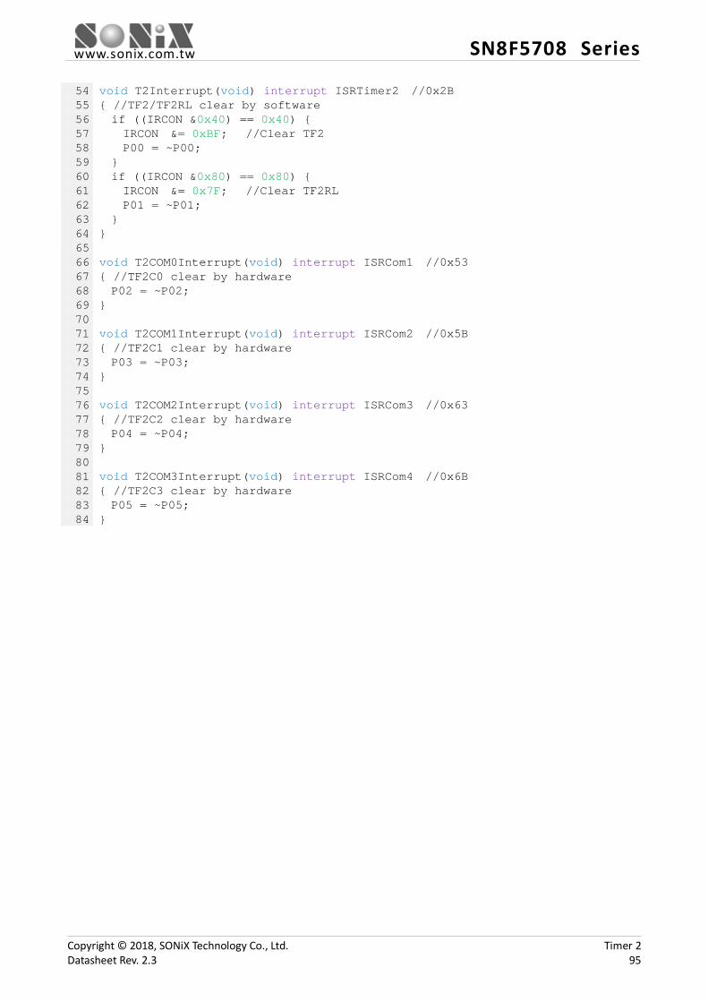
www.sonix.com.tw SN8F5708 Series
54 55 56 57 58 59 60 61 62 63 64 65 66 67 68 69 70 71 72 73 74 75 76 77 78 79 80 81 82 83 84
void T2Interrupt(void) interrupt ISRTimer2 //0x2B { //TF2/TF2RL clear by software if ((IRCON &0x40) == 0x40) { IRCON &= 0xBF; //Clear TF2 P00 = ~P00;
} if ((IRCON &0x80) == 0x80) { IRCON &= 0x7F; //Clear TF2RL P01 = ~P01;
} } void T2COM0Interrupt(void) interrupt ISRCom1 //0x53 { //TF2C0 clear by hardware P02 = ~P02;
} void T2COM1Interrupt(void) interrupt ISRCom2 //0x5B { //TF2C1 clear by hardware P03 = ~P03;
} void T2COM2Interrupt(void) interrupt ISRCom3 //0x63 { //TF2C2 clear by hardware P04 = ~P04;
} void T2COM3Interrupt(void) interrupt ISRCom4 //0x6B { //TF2C3 clear by hardware P05 = ~P05;
}
Copyright © 2018, SONiX Technology Co., Ltd. Timer 2 Datasheet Rev. 2.3 95

www.sonix.com.tw SN8F5708 Series
16 PWM
The PW1/PW2/PW3 timer respectively includes a 16-bit binary up 2-channel PWM, and one pulse PWM function functions. By the counter reaches the up-boundary value (PW1Y/PW2Y/PW3Y), it clears its counter and triggers an interrupt signal. Each PWM’s dutycycle is controlled by PW1D/PW2D/PW3D register.
The PWMs also support one pulse output signal which can disables itself by the end of first PWM cycle. Thus, only one pulsewould be generated in this condition. The PWM has two programmable channels shared with GPIO pins and controlled by PWCH[1:0] bit. The output operation must be through enabled each bit/channel of PWCH[1:0] bits. The enabled PWM channel exchanges from GPIO to PWM output. When the PWCH[1:0] bits disables, the PWM channel returns to last status of GPIO mode. The PWM build in IDLE Mode wake-up function if interrupt enable.When PWM timer overflow occurs(counts from PWnY-1 toPWnY), PWMnF would be issued immediately which can read/write by firmware. PWMn interrupt function is controlled by EPWMn.
16-Bit Binary UpCounting Counter
PWM RatePWnEN
PWMOUTClear to 0x0000
PWnPO
fosc
PWMnF
PWnEN
Divider÷1 to ÷128
EN
16-BitComparator
PWnDData Buffer
ReloadPWnDH/PWnDL
16-BitComparator
PWnYData Buffer
PWMnF
ReloadPWnYH/PWnYL
PWMnF
S
R
PulseControl
MUX
MUXGPIO
GPIO
PWnENPWCHn0
PWNVn0
PWMn0
PWMn1
Dead BandControl
PWNVn1
PWnENPWCHn1
PWnBH/PWnBL
PWnA
PWM Time Out
16.1 General PWM
PWn timer builds in PWM function controlled by PWnEN and PWCH[1:0] bits. PWMn0, PWMn1 are output pins. The PWMn0, PWMn1 output pins are shared with GPIO pin controlled by PWCH[1:0] bits. When output PWM function, we must be set PWnEN =1. When PWM output signal synchronize finishes, the PWM channel exchanges from GPIO to PWM output. When PWnEN = 0, the PWM channel returns to GPIO mode and last status. PWM signal is generated from the result of PWnY and PWnD comparison combination. When PWnC counts from 0x0000, the PWM outputs high status which is the PWM initial status. PWnC is loaded new data from PWnY register to decide
Copyright © 2018, SONiX Technology Co., Ltd. PWM Datasheet Rev. 2.3 96
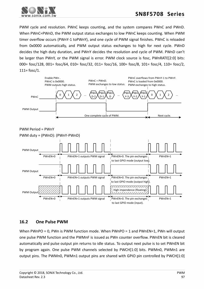
www.sonix.com.tw SN8F5708 Series
PWM cycle and resolution. PWnC keeps counting, and the system compares PWnC and PWnD. When PWnC=PWnD, the PWM output status exchanges to low PWnC keeps counting. When PWM timer overflow occurs (PWnY-1 toPWnY), and one cycle of PWM signal finishes. PWnC is reloaded from 0x0000 automatically, and PWM output status exchanges to high for next cycle. PWnD decides the high duty duration, and PWnY decides the resolution and cycle of PWM. PWnD can’t be larger than PWnY, or the PWM signal is error. PWM clock source is fosc, PWnRATE[2:0] bits: 000= fosc/128, 001= fosc/64, 010= fosc/32, 011= fosc/16, 100= fosc/8, 101= fosc/4, 110= fosc/2, 111= fosc/1.
0 1 2PWnC
... PWnD-2
PWnD-1
PWnD
PWM Output
... PWnY-3
PWnY-2
PWnY-1 0 1 2 ...
Enable PWn . PWnC is 0x0000.PWM outputs high status.
PWnC = PWnD. PWM exchanges to low status.
PWnC overflows from PWnY-1 to PWnY. PWnC is loaded from 0x0000.PWM exchanges to high status.
One complete cycle of PWM. Next cycle.
PWM Period = PWnY PWM duty = (PWnD): (PWnY-PWnD)
PWM Output
PWnEN=1 outputs PWM signal PWnEN=0. The pin exchanges to last GPIO mode (output low).
PWnEN=1PWnEN=0
PWM Output
PWnEN=0. The pin exchanges to last GPIO mode (output high).
PWnEN=1PWnEN=0
PWM Output
PWnEN=0. The pin exchanges to last GPIO mode (input).
PWnEN=1PWnEN=0
High impendence (floating)
PWnEN=1 outputs PWM signal
PWnEN=1 outputs PWM signal
16.2 One Pulse PWM
When PWnPO = 0, PWn is PWM function mode. When PWnPO = 1 and PWnEN=1, PWn will output one pulse PWM function and the PWMnF is issued as PWn counter overflow. PWnEN bit is cleared automatically and pulse output pin returns to idle status. To output next pulse is to set PWnEN bit by program again. One pulse PWM channels selected by PWCH[1:0] bits. PWMn0, PWMn1 are output pins. The PWMn0, PWMn1 output pins are shared with GPIO pin controlled by PWCH[1:0]
Copyright © 2018, SONiX Technology Co., Ltd. PWM Datasheet Rev. 2.3 97
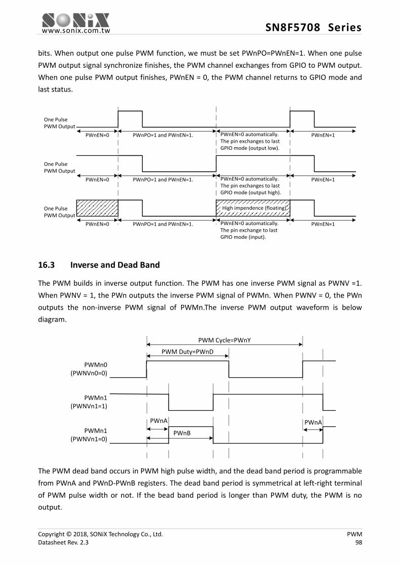
www.sonix.com.tw SN8F5708 Series
bits. When output one pulse PWM function, we must be set PWnPO=PWnEN=1. When one pulse PWM output signal synchronize finishes, the PWM channel exchanges from GPIO to PWM output. When one pulse PWM output finishes, PWnEN = 0, the PWM channel returns to GPIO mode and last status.
One PulsePWM Output
PWnPO=1 and PWnEN=1. PWnEN=0 automatically.The pin exchanges to lastGPIO mode (output low).
PWnEN=1PWnEN=0
PWnEN=1PWnEN=0
PWnEN=1PWnEN=0
High impendence (floating)
PWnEN=0 automatically.The pin exchange to lastGPIO mode (input).
PWnPO=1 and PWnEN=1.
PWnPO=1 and PWnEN=1.
PWnEN=0 automatically.The pin exchanges to lastGPIO mode (output high).
One PulsePWM Output
One PulsePWM Output
16.3 Inverse and Dead Band
The PWM builds in inverse output function. The PWM has one inverse PWM signal as PWNV =1. When PWNV = 1, the PWn outputs the inverse PWM signal of PWMn. When PWNV = 0, the PWn outputs the non-inverse PWM signal of PWMn.The inverse PWM output waveform is below diagram.
PWM Cycle=PWnY
PWM Duty=PWnD
PWMn1(PWNVn1=1)
PWnAPWMn1
(PWNVn1=0)PWnB
PWnA
PWMn0(PWNVn0=0)
The PWM dead band occurs in PWM high pulse width, and the dead band period is programmable from PWnA and PWnD-PWnB registers. The dead band period is symmetrical at left-right terminal of PWM pulse width or not. If the bead band period is longer than PWM duty, the PWM is no output.
Copyright © 2018, SONiX Technology Co., Ltd. PWM Datasheet Rev. 2.3 98

www.sonix.com.tw SN8F5708 Series
16.4 PWM Registers
Register Bit 7 Bit 6 Bit 5 Bit 4 Bit 3 Bit 2 Bit 1 Bit 0
PW1M PW1R2 PW1R1 PW1R0 PWNV11 PWNV10 PWCH11 PWCH10 PW1PO PW2M PW2R2 PW2R1 PW2R0 PWNV21 PWNV20 PWCH21 PWCH20 PW2PO PW3M PW3R2 PW3R1 PW3R0 PWNV31 PWNV30 PWCH31 PWCH30 PW3PO P1OC PW3EN PW2EN PW1EN P06OC P05OC P13OC P12OC P11OC
PW1YH PW1Y15 PW1Y14 PW1Y13 PW1Y12 PW1Y11 PW1Y10 PW1Y9 PW1Y8 PW1YL PW1Y7 PW1Y6 PW1Y5 PW1Y4 PW1Y3 PW1Y2 PW1Y1 PW1Y0 PW2YH PW2Y15 PW2Y14 PW2Y13 PW2Y12 PW2Y11 PW2Y10 PW2Y9 PW2Y8 PW2YL PW2Y7 PW2Y6 PW2Y5 PW2Y4 PW2Y3 PW2Y2 PW2Y1 PW2Y0 PW3YH PW3Y15 PW3Y14 PW3Y13 PW3Y12 PW3Y11 PW3Y10 PW3Y9 PW3Y8 PW3YL PW3Y7 PW3Y6 PW3Y5 PW3Y4 PW3Y3 PW3Y2 PW3Y1 PW3Y0 PW1DH PW1D15 PW1D14 PW1D13 PW1D12 PW1D11 PW1D10 PW1D9 PW1D8 PW1DL PW1D7 PW1D6 PW1D5 PW1D4 PW1D3 PW1D2 PW1D1 PW1D0 PW2DH PW2D15 PW2D14 PW2D13 PW2D12 PW2D11 PW2D10 PW2D9 PW2D8 PW2DL PW2D7 PW2D6 PW2D5 PW2D4 PW2D3 PW2D2 PW2D1 PW2D0 PW3DH PW3D15 PW3D14 PW3D13 PW3D12 PW3D11 PW3D10 PW3D9 PW3D8 PW3DL PW3D7 PW3D6 PW3D5 PW3D4 PW3D3 PW3D2 PW3D1 PW3D0 PW1BH PW1B15 PW1B14 PW1B13 PW1B12 PW1B11 PW1B10 PW1B9 PW1B8 PW1BL PW1B7 PW1B6 PW1B5 PW1B4 PW1B3 PW1B2 PW1B1 PW1B0 PW2BH PW2B15 PW2B14 PW2B13 PW2B12 PW2B11 PW2B10 PW2B9 PW2B8 PW2BL PW2B7 PW2B6 PW2B5 PW2B4 PW2B3 PW2B2 PW2B1 PW2B0 PW3BH PW3B15 PW3B14 PW3B13 PW3B12 PW3B11 PW3B10 PW3B9 PW3B8 PW3BL PW3B7 PW3B6 PW3B5 PW3B4 PW3B3 PW3B2 PW3B1 PW3B0 PW1A PW1A7 PW1A6 PW1A5 PW1A4 PW1A3 PW1A2 PW1A1 PW1A0 PW2A PW2A7 PW2A6 PW2A5 PW2A4 PW2A3 PW2A2 PW2A1 PW2A0 PW3A PW3A7 PW3A6 PW3A5 PW3A4 PW3A3 PW3A2 PW3A1 PW3A0 OPM PW3CM1 PW3CM0 PW2CM1 PW2CM0 PW1CM1 PW1CM0 OP1EN OP0EN IEN0 EAL - ET2 ES0 ET1 EX1 ET0 EX0 IEN2 - - ECMP1 ECMP0 EADC EPWM3 EPWM2 - IEN4 EPWM1 EX2 - - PWM1F IE2 - -
IRCON2 - - - CMP1F CMP0F ADCF PWM3F PWM2F
Copyright © 2018, SONiX Technology Co., Ltd. PWM Datasheet Rev. 2.3 99

www.sonix.com.tw SN8F5708 Series
PWnM Registers (PW1M: 0xAB, PW2M: 0xA1, PW3M: 0xB1) Bit Field Type Initial Description 7..5 PWnRATE R/W 000 PWM timer clock source
000: fosc / 128 001: fosc / 64 010 fosc / 32 011: fosc / 16 100: fosc / 8 101: fosc / 4 110: fosc / 2 111: fosc / 1
4 PWNVn1 R/W 0 PWMn1 pin output control 0: Non-inverse 1: Inverse
3 PWNVn0 R/W 0 PWMn0 pin output control 0: Non-inverse 1: Inverse
2 PWCHn1 R/W 0 PWMn1 shared-pin control 0: GPIO 1: PWM output
1 PWCHn0 R/W 0 PWMn0 shared-pin control 0: GPIO 1: PWM output
0 PWnPO R/W 0 One pulse function 0: Disable 1: Enable
Copyright © 2018, SONiX Technology Co., Ltd. PWM Datasheet Rev. 2.3 100

www.sonix.com.tw SN8F5708 Series
P1OC Register (0xE4) Bit Field Type Initial Description 7 PW3EN R/W 0 PW3 function
0: Disable 1: Enable
6 PW2EN R/W 0 PW2 function 0: Disable 1: Enable
5 PW1EN R/W 0 PW1 function 0: Disable 1: Enable
Else Refer to other chapter(s) PW1YH/PW1YL Registers (PW1YH: 0xAD, PW1YL: 0xAC) Bit Field Type Initial Description 7..0 PW1YH/L R/W 0x00 16-bit PWM1 period control
PW2YH/PW2YL Registers (PW2YH: 0xA3, PW2YL: 0xA2) Bit Field Type Initial Description 7..0 PW2YH/L R/W 0x00 16-bit PWM2 period control
PW3YH/PW3YL Registers (PW3YH: 0xB3, PW3YL: 0xB2) Bit Field Type Initial Description 7..0 PW3YH/L R/W 0x00 16-bit PWM3 period control
PW1DH/PW1DL Registers (PW1DH: 0xBC, PW1DL: 0xBB) Bit Field Type Initial Description 7..0 PW1DH/L R/W 0x00 16-bit PWM1 duty control
PW2DH/PW2DL Registers (PW2DH: 0xA7, PW2DL: 0xA6) Bit Field Type Initial Description 7..0 PW2DH/L R/W 0x00 16-bit PWM2 duty control
Copyright © 2018, SONiX Technology Co., Ltd. PWM Datasheet Rev. 2.3 101
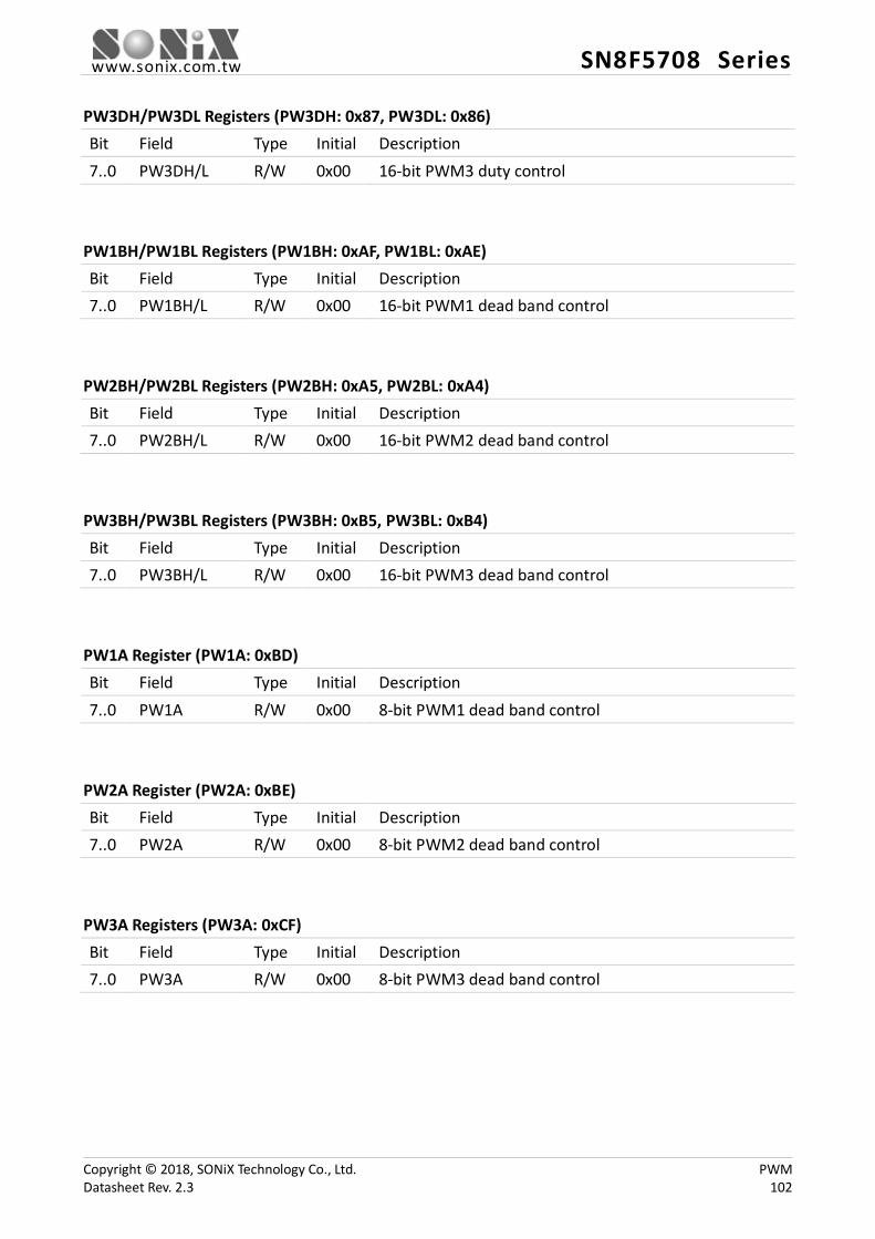
www.sonix.com.tw SN8F5708 Series
PW3DH/PW3DL Registers (PW3DH: 0x87, PW3DL: 0x86) Bit Field Type Initial Description 7..0 PW3DH/L R/W 0x00 16-bit PWM3 duty control
PW1BH/PW1BL Registers (PW1BH: 0xAF, PW1BL: 0xAE) Bit Field Type Initial Description 7..0 PW1BH/L R/W 0x00 16-bit PWM1 dead band control
PW2BH/PW2BL Registers (PW2BH: 0xA5, PW2BL: 0xA4) Bit Field Type Initial Description 7..0 PW2BH/L R/W 0x00 16-bit PWM2 dead band control
PW3BH/PW3BL Registers (PW3BH: 0xB5, PW3BL: 0xB4) Bit Field Type Initial Description 7..0 PW3BH/L R/W 0x00 16-bit PWM3 dead band control
PW1A Register (PW1A: 0xBD) Bit Field Type Initial Description 7..0 PW1A R/W 0x00 8-bit PWM1 dead band control
PW2A Register (PW2A: 0xBE) Bit Field Type Initial Description 7..0 PW2A R/W 0x00 8-bit PWM2 dead band control
PW3A Registers (PW3A: 0xCF) Bit Field Type Initial Description 7..0 PW3A R/W 0x00 8-bit PWM3 dead band control
Copyright © 2018, SONiX Technology Co., Ltd. PWM Datasheet Rev. 2.3 102
www.sonix.com.tw SN8F5708 Series
OPM Register (0x9B) Bit Field Type Initial Description 7 PW3CM1 R/W 0 PWM3 output and CMP1 trigger synchronous control bit
0: Disable 1: Enable
6 PW3CM0 R/W 0 PWM3 output and CMP0 trigger synchronous control bit 0: Disable 1: Enable
5 PW2CM1 R/W 0 PWM2 output and CMP1 trigger synchronous control bit 0: Disable 1: Enable
4 PW2CM0 R/W 0 PWM2 output and CMP0 trigger synchronous control bit 0: Disable 1: Enable
3 PW1CM1 R/W 0 PWM1 output and CMP1 trigger synchronous control bit 0: Disable 1: Enable
2 PW1CM0 R/W 0 PWM1 output and CMP0 trigger synchronous control bit 0: Disable 1: Enable
Else Refer to other chapter(s) IEN0 Register (0xA8) Bit Field Type Initial Description 7 EAL R/W 0 Interrupts enable. Refer to Chapter Interrupt Else Refer to other chapter(s)
IEN2 Register (0X9A) Bit Field Type Initial Description 2 EPWM3 R/W 0 PWM3 interrupt control bit.
0: Disable PWM3 interrupt function. 1: Enable PWM3 interrupt function.
1 EPWM2 R/W 0 PWM2interrupt control bit 0: Disable PWM2 interrupt function. 1: Enable PWM2 interrupt function.
Else Reserved R 0
Copyright © 2018, SONiX Technology Co., Ltd. PWM Datasheet Rev. 2.3 103

www.sonix.com.tw SN8F5708 Series
IEN4 Register (0XD1) Bit Field Type Initial Description 7 EPWM1 R/W 0 PWM1 interrupt control bit.
0 = Disable PWM1 interrupt function. 1 = Enable PWM1 interrupt function.
3 PWM1F R/W 0 PWM1interrupt request flag. 0: None PWM1 interrupt request 1:PWM1 interrupt request.
Else Reserved R 0 IRCON2 Register (0XBF) Bit Field Type Initial Description 1 PWM3F R/W 0 PWM3interrupt request flag.
0: None PWM3 interrupt request 1:PWM3 interrupt request.
0 PWM2F R/W 0 PWM2interrupt request flag. 0: None PWM2 interrupt request 1:PWM2 interrupt request.
Else Reserved R 0
Copyright © 2018, SONiX Technology Co., Ltd. PWM Datasheet Rev. 2.3 104

www.sonix.com.tw SN8F5708 Series
16.5 Sample Code
The following sample code demonstrates how to perform PW1/PW2/PW3 with interrupt.
1 2 3 4 5 6 7 8 9 10 11 12 13 14 15 16 17 18 19 20 21 22 23 24 25 26 27 28 29 30 31 32 33 34 35 36 37 38 39 40 41 42 43 44 45 46 47 48 49 50 51 52 53
#define PW1Inv0(1<<3) //PWM10 output inverse #define PW1Inv1(1<<4) //PWM11 output inverse #define PW1CMP0Tri (1<<2) //PW1 output Control by Comparator 0 trigger #define PW1CMP1Tri (1<<3) //PW1 output Control by Comparator 1 trigger #define PW1OnePu (1<<0) //Enable PW1 pulse output function #define PWM10En (1<<1) //Enable PWM10 output function #define PWM11En (1<<2) //Enable PWM11 output function #define PW1En (1<<5) //Enable PWM1 function #define PW2Inv0 (1<<3) //PWM20 output inverse #define PW2Inv1 (1<<4) //PWM21 output inverse #define PW2CMP0Tri (1<<4) //PW2 output Control by Comparator 0 trigger #define PW2CMP1Tri (1<<5) //PW2 output Control by Comparator 1 trigger #define PW2OnePu (1<<0) //Enable PW2 pulse output function #define PWM20En (1<<1) //Enable PWM20 output function #define PWM21En (1<<2) //Enable PWM21 output function #define PW2En (1<<6) //Enable PWM2 function #define PW3Inv0 (1<<3) //PWM30 output inverse #define PW3Inv1 (1<<4) //PWM31 output inverse #define PW3CMP0Tri (1<<6) //PW3 output Control by Comparator 0 trigger #define PW3CMP1Tri (1<<7) //PW3 output Control by Comparator 1 trigger #define PW3OnePu (1<<0) //Enable PW3 pulse output function #define PWM30En (1<<1) //Enable PWM30 output function #define PWM31En (1<<2) //Enable PWM31 output function #define PW3En (1<<7) //Enable PWM3 function void InitPWM(void) { // PWM1_Initial PW1YH = 0x80; PW1YL = 0x00; PW1DH = 0x40; PW1DL = 0x00; PW1BH = 0x60; PW1BL = 0x00; PW1A = 0x80; // PWM1 clock = Fosc/32, PW10/11 channel enable PW1M = 0x40 | PWM10En | PWM11En; // PWM2_Initial PW2YH = 0x00; PW2YL = 0x80; PW2DH = 0x00; PW2DL = 0x40; PW2BH = 0x00; PW2BL = 0x60; PW2A = 0x20; // PWM2 clock = Fosc/128, PW20/21 channel enable with inverse PW2M = 0x00 | PW2Inv0 | PW2Inv1 | PWM20En | PWM21En;
Copyright © 2018, SONiX Technology Co., Ltd. PWM Datasheet Rev. 2.3 105

www.sonix.com.tw SN8F5708 Series
54 55 56 57 58 59 60 61 62 63 64 65 66 67 68 69 70 71 72 73 74 75 76 77 78 79 80 81 82 83 84 85 86 87 88 89 90 91 92 93 94 95 96 97 98 99 100 101 102 103 104 105
// PWM3_Initial PW3YH = 0xF0; PW3YL = 0xF0; PW3DH = 0x80; PW3DL = 0x80; PW3BH = 0x40; PW3BL = 0x40; PW3A = 0xF0; // PWM3 clock = Fosc/1, PW30/31 channel enable with one pulse PW3M = 0xE0 | PWM30En | PWM31En | PW3OnePu; // PW1/PW2/PW3 enable P1OC|= PW3En | PW2En | PW1En; // Enable PWM1 interrupt IEN4|= 0x80; // Enable PWM2/PWM3 interrupt IEN2|= 0x06; // Enable total interrupt IEN0 |= 0x80; P0 = 0x00; P0M |= 0x07;
} void PW1Interrupt(void) interrupt ISRPwm1 //0x83 { //PWM1F clear by software if ((IEN4&0x08) == 0x08) { IEN4&= 0xF7; //Clear PWM1F P00 = ~P00;
} } void PW2Interrupt(void) interrupt ISRPwm2 //0x8B { //PWM2F clear by software if ((IRCON2&0x01) == 0x01) { IRCON2&= 0xFE; //Clear PWM2F P01 = ~P01;
} } void PW3Interrupt(void) interrupt ISRPwm3 //0x93 { //PWM3F clear by software if ((IRCON2&0x02) == 0x02) { IRCON2&= 0xFD; //Clear PWM3F P02 = ~P02;
} }
Copyright © 2018, SONiX Technology Co., Ltd. PWM Datasheet Rev. 2.3 106
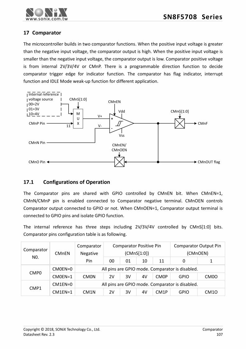
www.sonix.com.tw SN8F5708 Series
17 Comparator
The microcontroller builds in two comparator functions. When the positive input voltage is greater than the negative input voltage, the comparator output is high. When the positive input voltage is smaller than the negative input voltage, the comparator output is low. Comparator positive voltage is from internal 2V/3V/4V or CMnP. There is a programmable direction function to decide comparator trigger edge for indicator function. The comparator has flag indicator, interrupt function and IDLE Mode weak-up function for different application.
CMnO Pin
CMnG[1:0]
CMnOUT flag
CMnF+
-
Vdd
Vss
V+
V-CMnP Pin
CMnN Pin CMnEN/CMnOEN
CMnEN
Internal reference voltage source 00=2V01=3V10=4V
CMnS[1:0]
11
MUX
17.1 Configurations of Operation
The Comparator pins are shared with GPIO controlled by CMnEN bit. When CMnEN=1, CMnN/CMnP pin is enabled connected to Comparator negative terminal. CMnOEN controls Comparator output connected to GPIO or not. When CMnOEN=1, Comparator output terminal is connected to GPIO pins and isolate GPIO function.
The internal reference has three steps including 2V/3V/4V controlled by CMnS[1:0] bits. Comparator pins configuration table is as following.
Comparator N0.
CMnEN Comparator
Negative Pin
Comparator Positive Pin (CMnS[1:0])
Comparator Output Pin (CMnOEN)
00 01 10 11 0 1
CMP0 CM0EN=0 All pins are GPIO mode. Comparator is disabled. CM0EN=1 CM0N 2V 3V 4V CM0P GPIO CM0O
CMP1 CM1EN=0 All pins are GPIO mode. Comparator is disabled. CM1EN=1 CM1N 2V 3V 4V CM1P GPIO CM1O
Copyright © 2018, SONiX Technology Co., Ltd. Comparator Datasheet Rev. 2.3 107

www.sonix.com.tw SN8F5708 Series
17.2 Comparator Output Function
The comparator output signal is the source of comparator output function. The comparator output function includes:
CMnOUT output flag: The comparator output signal is connected to CMnOUT flag directly. CMnOUT bit responses comparator status immediately. Program reads comparator status from CMnOUT bit.
Comparator extern pin output function: The comparator output status can output to CMnO pin controlled by CMnOEN bit. When CMnOEN=0, the comparator output pin is GPIO mode. If CMnOEN=1, CMnO pin outputs comparator output status and isolates GPIO mode.
Comparator edge trigger and interrupt function: The comparator builds in interrupt function, and the trigger edge is programmable. CMnG[1:0] bit controls comparator trigger edge. When the edge trigger condition occurs, CMPnF will be set automatically. To clear CMPnF bit must be through program. If CMnEN=1, program counter will be pointed to interrupt vector to execute interrupt service routine as CMPnF is setting. When the trigger edge direction is equal to interrupt trigger condition, the system will execute interrupt operation immediately.
Comparator IDLE Mode Wake-up function: The comparator’s wake-up function only support IDLE Mode (interrupt needs enable), not STOP Mode. If the trigger edge condition (comparator output status exchanging) is found, the system will be wake-up from IDLE Mode. Because in interrupt trigger condition, the CMPnF is set as “1”. Of course the interrupt routine is executed if the interrupt function enabled.
17.3 PWM Output Control
The results of comparator can be used to control PWM outputs. User can select the appropriate control mode through CMPT register. The following table lists these types of control methods.
CMnT[1:0] PWM Synchronous Trigger Operation 00 CMPn with PWM output is not related. 01 CMPnF = 1 PWM stop
10 CMnP > CMnN (Rising edge trigger) PWM output CMnP < CMnN (Falling edge trigger) PWM stop
11 CMnP < CMnN (Falling edge trigger) PWM output
CMnP > CMnN (rising edge trigger) PWM stop
The comparator can control those PWM outputs, depending PWnCM* bits set. See detailed description of PWM section.OPM register bit 7 – 2: PW3CM1, PW3CM0, PW2CM0, PW2CM1, PW1CM1, PW1CM0.
Copyright © 2018, SONiX Technology Co., Ltd. Comparator Datasheet Rev. 2.3 108
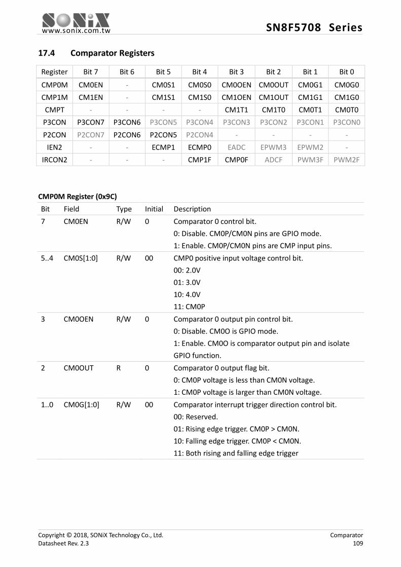
www.sonix.com.tw SN8F5708 Series
17.4 Comparator Registers
Register Bit 7 Bit 6 Bit 5 Bit 4 Bit 3 Bit 2 Bit 1 Bit 0
CMP0M CM0EN - CM0S1 CM0S0 CM0OEN CM0OUT CM0G1 CM0G0 CMP1M CM1EN - CM1S1 CM1S0 CM1OEN CM1OUT CM1G1 CM1G0 CMPT - - - - CM1T1 CM1T0 CM0T1 CM0T0
P3CON P3CON7 P3CON6 P3CON5 P3CON4 P3CON3 P3CON2 P3CON1 P3CON0 P2CON P2CON7 P2CON6 P2CON5 P2CON4 - - - -
IEN2 - - ECMP1 ECMP0 EADC EPWM3 EPWM2 - IRCON2 - - - CMP1F CMP0F ADCF PWM3F PWM2F
CMP0M Register (0x9C) Bit Field Type Initial Description 7 CM0EN R/W 0 Comparator 0 control bit.
0: Disable. CM0P/CM0N pins are GPIO mode. 1: Enable. CM0P/CM0N pins are CMP input pins.
5..4 CM0S[1:0] R/W 00 CMP0 positive input voltage control bit. 00: 2.0V 01: 3.0V 10: 4.0V 11: CM0P
3 CM0OEN R/W 0 Comparator 0 output pin control bit. 0: Disable. CM0O is GPIO mode. 1: Enable. CM0O is comparator output pin and isolate GPIO function.
2 CM0OUT R 0 Comparator 0 output flag bit. 0: CM0P voltage is less than CM0N voltage. 1: CM0P voltage is larger than CM0N voltage.
1..0 CM0G[1:0] R/W 00 Comparator interrupt trigger direction control bit. 00: Reserved. 01: Rising edge trigger. CM0P > CM0N. 10: Falling edge trigger. CM0P < CM0N. 11: Both rising and falling edge trigger
Copyright © 2018, SONiX Technology Co., Ltd. Comparator Datasheet Rev. 2.3 109
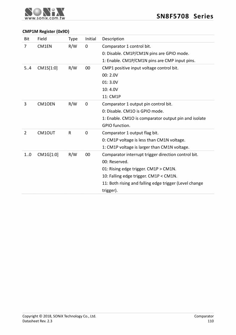
www.sonix.com.tw SN8F5708 Series
CMP1M Register (0x9D) Bit Field Type Initial Description 7 CM1EN R/W 0 Comparator 1 control bit.
0: Disable. CM1P/CM1N pins are GPIO mode. 1: Enable. CM1P/CM1N pins are CMP input pins.
5..4 CM1S[1:0] R/W 00 CMP1 positive input voltage control bit. 00: 2.0V 01: 3.0V 10: 4.0V 11: CM1P
3 CM1OEN R/W 0 Comparator 1 output pin control bit. 0: Disable. CM1O is GPIO mode. 1: Enable. CM1O is comparator output pin and isolate GPIO function.
2 CM1OUT R 0 Comparator 1 output flag bit. 0: CM1P voltage is less than CM1N voltage. 1: CM1P voltage is larger than CM1N voltage.
1..0 CM1G[1:0] R/W 00 Comparator interrupt trigger direction control bit. 00: Reserved. 01: Rising edge trigger. CM1P > CM1N. 10: Falling edge trigger. CM1P < CM1N. 11: Both rising and falling edge trigger (Level change trigger).
Copyright © 2018, SONiX Technology Co., Ltd. Comparator Datasheet Rev. 2.3 110

www.sonix.com.tw SN8F5708 Series
CMPT Register (0xCE) Bit Field Type Initial Description 3..2 CM1T[1:0] R/W 00 CMP1 with PWM trigger select bits.
00: CMP1 with PWM output is not related. 01: CMP1F = 1 PWM stop 10: CM1P > CM1N PWM output; CM1P < CM1N PWM stop 11: CM1P < CM1NPWM output; CM1P > CM1NPWM stop
1..0 CM0T[1:0] R/W 00 CMP0 with PWM trigger select bits. 00: CMP0 with PWM output is not related. 01: CMP0F = 1 PWM stop 10: CM0P > CM0N PWM output; CM0P < CM0N PWM stop 11: CM0P < CM0N PWM output; CM0P > CM0N PWM stop
P3CON Register (0x9F) Bit Field Type Initial Description 7..6 P3CON[7:6] R/W 0x00 P3 configuration control bit*.
0: P3 can be analog input pin (CMP input pin) or digital GPIO pin. 1: P3 is pure analog input pin and can’t be a digital GPIO pin.
5..0 Refer to other chapter(s) * P3CON [7:6] will configure related Port3 pin as pure analog input pin to avoid current leakage.
P2CON Register (0x9E) Bit Field Type Initial Description
6..5 P2CON[6:5] R/W 0x0 P2 configuration control bit*.
0: P2 can be analog input pin (CMP input pin) or digital GPIO pin.
1: P2 is pure analog input pin and can’t be a digital GPIO pin.
Else Refer to other chapter(s) * P2CON [6:5] will configure related Port2 pin as pure analog input pin to avoid current leakage.
Copyright © 2018, SONiX Technology Co., Ltd. Comparator Datasheet Rev. 2.3 111
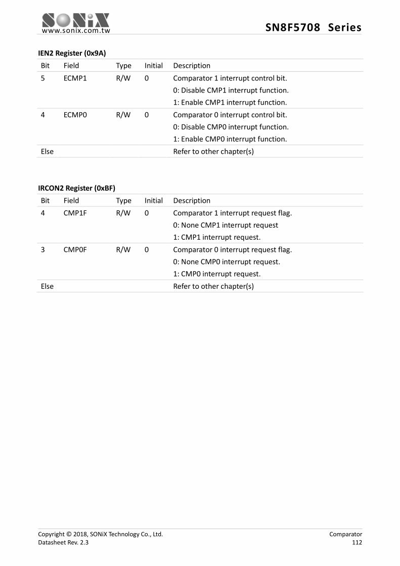
www.sonix.com.tw SN8F5708 Series
IEN2 Register (0x9A) Bit Field Type Initial Description 5 ECMP1 R/W 0 Comparator 1 interrupt control bit.
0: Disable CMP1 interrupt function. 1: Enable CMP1 interrupt function.
4 ECMP0 R/W 0 Comparator 0 interrupt control bit. 0: Disable CMP0 interrupt function. 1: Enable CMP0 interrupt function.
Else Refer to other chapter(s) IRCON2 Register (0xBF) Bit Field Type Initial Description 4 CMP1F R/W 0 Comparator 1 interrupt request flag.
0: None CMP1 interrupt request 1: CMP1 interrupt request.
3 CMP0F R/W 0 Comparator 0 interrupt request flag. 0: None CMP0 interrupt request. 1: CMP0 interrupt request.
Else Refer to other chapter(s)
Copyright © 2018, SONiX Technology Co., Ltd. Comparator Datasheet Rev. 2.3 112
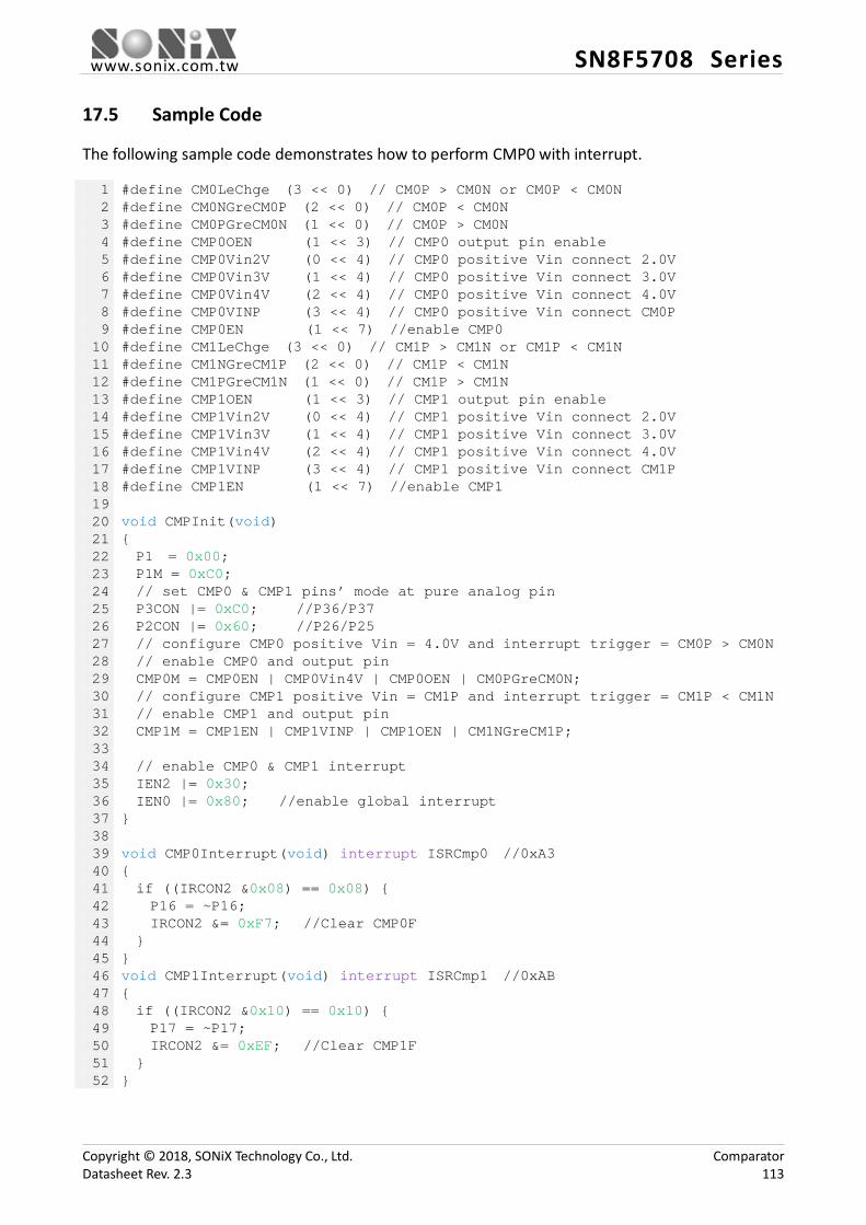
www.sonix.com.tw SN8F5708 Series
17.5 Sample Code
The following sample code demonstrates how to perform CMP0 with interrupt.
1 2 3 4 5 6 7 8 9 10 11 12 13 14 15 16 17 18 19 20 21 22 23 24 25 26 27 28 29 30 31 32 33 34 35 36 37 38 39 40 41 42 43 44 45 46 47 48 49 50 51 52
#define CM0LeChge (3 << 0) // CM0P > CM0N or CM0P < CM0N #define CM0NGreCM0P (2 << 0) // CM0P < CM0N #define CM0PGreCM0N (1 << 0) // CM0P > CM0N #define CMP0OEN (1 << 3) // CMP0 output pin enable #define CMP0Vin2V (0 << 4) // CMP0 positive Vin connect 2.0V #define CMP0Vin3V (1 << 4) // CMP0 positive Vin connect 3.0V #define CMP0Vin4V (2 << 4) // CMP0 positive Vin connect 4.0V #define CMP0VINP (3 << 4) // CMP0 positive Vin connect CM0P #define CMP0EN (1 << 7) //enable CMP0 #define CM1LeChge (3 << 0) // CM1P > CM1N or CM1P < CM1N #define CM1NGreCM1P (2 << 0) // CM1P < CM1N #define CM1PGreCM1N (1 << 0) // CM1P > CM1N #define CMP1OEN (1 << 3) // CMP1 output pin enable #define CMP1Vin2V (0 << 4) // CMP1 positive Vin connect 2.0V #define CMP1Vin3V (1 << 4) // CMP1 positive Vin connect 3.0V #define CMP1Vin4V (2 << 4) // CMP1 positive Vin connect 4.0V #define CMP1VINP (3 << 4) // CMP1 positive Vin connect CM1P #define CMP1EN (1 << 7) //enable CMP1 void CMPInit(void) { P1 = 0x00; P1M = 0xC0; // set CMP0 & CMP1 pins’ mode at pure analog pin P3CON |= 0xC0; //P36/P37 P2CON |= 0x60; //P26/P25
// configure CMP0 positive Vin = 4.0V and interrupt trigger = CM0P > CM0N // enable CMP0 and output pin CMP0M = CMP0EN | CMP0Vin4V | CMP0OEN | CM0PGreCM0N; // configure CMP1 positive Vin = CM1P and interrupt trigger = CM1P < CM1N // enable CMP1 and output pin CMP1M = CMP1EN | CMP1VINP | CMP1OEN | CM1NGreCM1P;
// enable CMP0 & CMP1 interrupt IEN2 |= 0x30; IEN0 |= 0x80; //enable global interrupt
} void CMP0Interrupt(void) interrupt ISRCmp0 //0xA3 { if ((IRCON2 &0x08) == 0x08) { P16 = ~P16; IRCON2 &= 0xF7; //Clear CMP0F
} } void CMP1Interrupt(void) interrupt ISRCmp1 //0xAB { if ((IRCON2 &0x10) == 0x10) { P17 = ~P17; IRCON2 &= 0xEF; //Clear CMP1F
} }
Copyright © 2018, SONiX Technology Co., Ltd. Comparator Datasheet Rev. 2.3 113
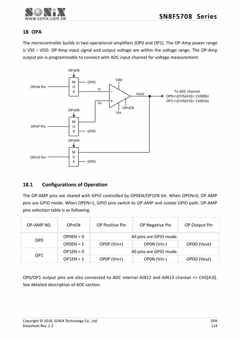
www.sonix.com.tw SN8F5708 Series
18 OPA
The microcontroller builds in two operational amplifiers (OP0 and OP1). The OP-Amp power range is VSS – VDD. OP-Amp input signal and output voltage are within the voltage range. The OP-Amp output pin is programmable to connect with ADC input channel for voltage measurement.
+
-
Vdd
Vss
Vout
V+
V-OPnN Pin
OPnEN
OPnP Pin
OPnO Pin
OPnENOPnEN
To ADC channel OP0=>(CHS[4:0]= 11000b)OP1=>(CHS[4:0]= 11001b)
MUX GPIO
MUX
GPIO
OPnEN
MUX GPIO
18.1 Configurations of Operation
The OP-AMP pins are shared with GPIO controlled by OP0EN/OP1EN bit. When OPEN=0, OP AMP pins are GPIO mode. When OPEN=1, GPIO pins switch to OP-AMP and isolate GPIO path. OP-AMP pins selection table is as following.
OP-AMP N0. OPnEN OP Positive Pin OP Negative Pin OP Output Pin
OP0 OP0EN = 0 All pins are GPIO mode. OP0EN = 1 OP0P (Vin+) OP0N (Vin-) OP0O (Vout)
OP1 OP1EN = 0 All pins are GPIO mode. OP1EN = 1 OP0P (Vin+) OP0N (Vin-) OP0O (Vout)
OP0/OP1 output pins are also connected to ADC internal AIN12 and AIN13 channel => CHS[4:0]. See detailed description of ADC section.
Copyright © 2018, SONiX Technology Co., Ltd. OPA Datasheet Rev. 2.3 114
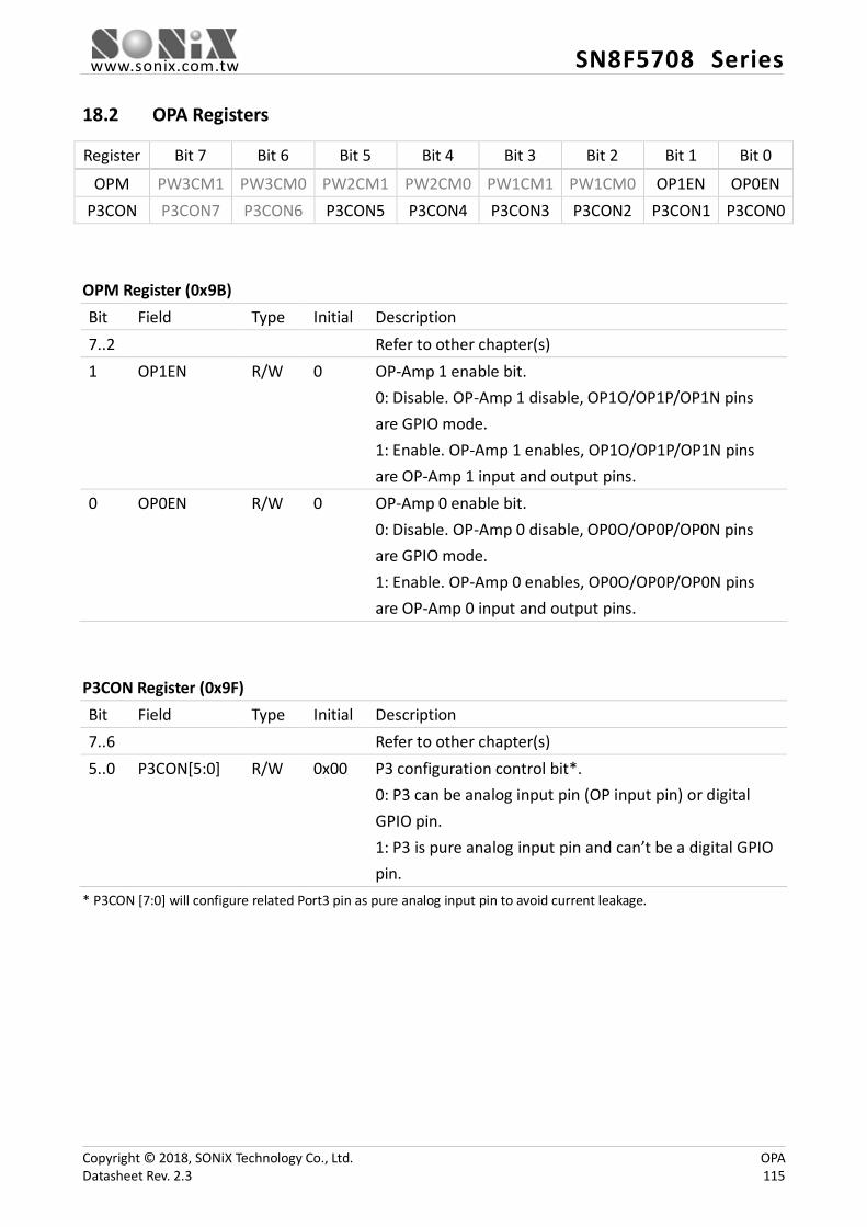
www.sonix.com.tw SN8F5708 Series
18.2 OPA Registers
Register Bit 7 Bit 6 Bit 5 Bit 4 Bit 3 Bit 2 Bit 1 Bit 0
OPM PW3CM1 PW3CM0 PW2CM1 PW2CM0 PW1CM1 PW1CM0 OP1EN OP0EN P3CON P3CON7 P3CON6 P3CON5 P3CON4 P3CON3 P3CON2 P3CON1 P3CON0
OPM Register (0x9B) Bit Field Type Initial Description 7..2 Refer to other chapter(s) 1 OP1EN R/W 0 OP-Amp 1 enable bit.
0: Disable. OP-Amp 1 disable, OP1O/OP1P/OP1N pins are GPIO mode. 1: Enable. OP-Amp 1 enables, OP1O/OP1P/OP1N pins are OP-Amp 1 input and output pins.
0 OP0EN R/W 0 OP-Amp 0 enable bit. 0: Disable. OP-Amp 0 disable, OP0O/OP0P/OP0N pins are GPIO mode. 1: Enable. OP-Amp 0 enables, OP0O/OP0P/OP0N pins are OP-Amp 0 input and output pins.
P3CON Register (0x9F) Bit Field Type Initial Description 7..6 Refer to other chapter(s) 5..0 P3CON[5:0] R/W 0x00 P3 configuration control bit*.
0: P3 can be analog input pin (OP input pin) or digital GPIO pin. 1: P3 is pure analog input pin and can’t be a digital GPIO pin.
* P3CON [7:0] will configure related Port3 pin as pure analog input pin to avoid current leakage.
Copyright © 2018, SONiX Technology Co., Ltd. OPA Datasheet Rev. 2.3 115
www.sonix.com.tw SN8F5708 Series
18.3 Sample Code
The following sample code demonstrates how to perform OP0.
1 2 3 4 5 6 7 8 9 10 11 12 13 14 15 16 17 18 19 20
#define OP0EN (1 << 0) #define OP1EN (1<<1) void OP0En(void) { // set OP0 pins’ mode at pure analog pin P3CON = 0x07; // enable OP0 OPM |= OP0EN; } void OP1En(void) { // set OP1 pins’ mode at pure analog pin P3CON = 0x38; // enable OP1 OPM |= OP1EN; }
Copyright © 2018, SONiX Technology Co., Ltd. OPA Datasheet Rev. 2.3 116

www.sonix.com.tw SN8F5708 Series
19 ADC
The analog to digital converter (ADC) is SAR structure with 12-input sources and up to 4096-step resolution to transfer analog signal into 12-bits digital buffers. The ADC builds in 12-channel input source to measure 12 different analog signal sources. The ADC resolution is 12-bit. The ADC has four clock rates to decide ADC converting rate. The ADC reference high voltage includes 5 sources. Four internal power source including VDD, 4V, 3V and 2V. The other one is external reference voltage input pin from AVREFH pin. The ADC reference low voltage includes 2 sources controlled by VREFH register. One is internal VSS and the other one is external reference voltage input pin from AVREFL. The ADC builds in P2CON/P3CON/P4CON/P5CON registers to set pure analog input pin. After setup ADENB and ADS bits, the ADC starts to convert analog signal to digital data. Besides ADS bit can start to convert analog signal, PW1EN/ PW2EN/ PW3EN also have convert analog signal ADC function. ADC can work in idle mode. After ADC operating, the system would be waked up from green mode to normal mode if interrupt enable.
AIN0
MUX
CHS[4:0]
GCHS
ADC High Reference Voltage
Analog Input
ADENB ADS/PW1EN/PW2EN/PW3EN
ADC ClockCounter
ADCKS[1:0]
ADB[11:0]
EOC
ADCF
12
Internal reference
External reference
EVHENB, ADCENB
VHS[2:0]
Internal Reference Voltage Source
(2V, 3V, 4V, VDD)
(2V, 3V, 4V)VHS[1:0]
ADC Low Reference Voltage
AVREFL
Internal Vss
AVREFH
Trigger source
(interrupt flag)
AIN1AIN2AIN3AIN4AIN5AIN6AIN7AIN8AIN9AIN10AIN11
OP0 outputOP1 output
MUX
MUX
EVLENB
SAR ADC ENGINE
Copyright © 2018, SONiX Technology Co., Ltd. ADC Datasheet Rev. 2.3 117
www.sonix.com.tw SN8F5708 Series
19.1 Configurations of Operation
These configurations must be setup completely before starting ADC converting.ADC is configured using the following steps: 1. Choose and enable the start of conversion ADC input channel. (By CHS[4:0] bits and GCHS bit) 2. The GPIO mode of ADC input channel must be set as input mode. (By PnM register) 3. The internal pull-up resistor of ADC input channel must be disabled. (By PnUR register) 4. The configuration control bit of ADC input channel must be set. (By PnCON register) 5. Choose ADC high reference voltage and low reference Voltage. (By VREFH register) 6. Choose ADC Clock Rate. (By ADCKS[1:0] bits) 7. After setup ADENB bits, the ADC ready to convert analog signal to digital data. 19.1.1 Start to Conversion
When ADC IP is enabled by ADENB bit, it is necessary to make a ADC start-up by program. Besides ADS bit can start to convert analog signal, PW1EN/PW2EN/PW3EN also have convert analog signal ADC function. Conversions may be initiated by one of the following: Writing a 1 to the ADS bit of register ADM PWM1 was enabled when ADPWS bit is “1” PWM2 was enabled when ADPWS bit is “1” PWM3 was enabled when ADPWS bit is “1” After setup ADENB and ADS bits, the ADC starts to convert analog signal to digital data. The ADS bit is reset to logic 0 when the conversion is complete.When the conversion is complete, the ADC circuit will set EOC and ADCF bits to “1” and the digital data outputs in ADB and ADR registers.If ADC interrupt function is enabled (EADC = 1), the ADC interrupt request occurs and executes interrupt service routine when ADCF is “1” after ADC converting. Clear ADCF by program is necessary in interrupt procedure.Note that when ADPWS bit is “1”, if PWM enable trigger be used as the conversion source, the ADC will continuous conversions until PWM is disabled.
19.2 ADC input channel
The ADC builds in 12-channel input source (AIN0 – AIN11) to measure 12 different analog signal sources controlled by CHS[4:0] and GCHS bits.AIN12, AIN13 channels are OP0 and OP1-Amp output terminal. The AIN14 is internal 2V or 3V or 4V input channel. There is no any input pin from outside. In this time ADC reference voltage must be internal VDD and External voltage, not internal 2V or 3V or 4V. AIN14 can be a good battery detector for battery system. To select appropriate internal AVREFH level and compare value, a high performance and cheaper low battery detector is built in the system.
Copyright © 2018, SONiX Technology Co., Ltd. ADC Datasheet Rev. 2.3 118

www.sonix.com.tw SN8F5708 Series
CHS[4:0] Channel Pin name Remark
00000 AIN0 P4.0 00001 AIN1 P4.1 00010 AIN2 P4.2 00011 AIN3 P4.3 00100 AIN4 P4.4 00101 AIN5 P4.5 00110 AIN6 P4.6 00111 AIN7 P4.7 01000 AIN8 P5.0 01001 AIN9 P5.1 01010 AIN10 P5.2 01011 AIN11 P5.3
01100 – 10111 - - Reserved 11000 AIN12 OP0 OP0-AMP output terminal 11001 AIN13 OP1 OP1-AMP output terminal 11010 AIN14 Internal 2V or 3V or 4V Battery detector channel
11011 – 11111 - - No connection
19.2.1 PinConfiguration
ADC input channels are shared with Port2, Port3, Port4 and Port5. ADC channel selection is through CHS[4:0] bit. Only one pin of Port2, Port3, Port4 and Port5 can be configured as ADC input in the same time. The pins of Port2, Port3, Port4 and Port5 configured as ADC input channel must be set input mode, disable internal pull-up and enable P2CON/P3CON/P4CON/P5CON first by program. After selecting ADC input channel through CHS[4:0], set GCHS bit as “1” to enable ADC channel function.
ADC input pins are shared with digital I/O pins. Connect an analog signal to CMOS digital input pin, especially, the analog signal level is about 1/2 VDD will cause extra current leakage. In the power down mode, the above leakage current will be a big problem. Unfortunately, if users connect more than one analog input signal to Port2, Port3, Port4 or Port5 will encounter above current leakage situation. Write “1” into PnCON register will configure related pin as pure analog input pin to avoid current leakage.
Note that When ADC pin is general I/O mode, the bit of P2CON, P3CON, P4CON and P5CON must be set to “0”, or the digital I/O signal would be isolated.
Copyright © 2018, SONiX Technology Co., Ltd. ADC Datasheet Rev. 2.3 119

www.sonix.com.tw SN8F5708 Series
19.3 Reference Voltage
The ADC builds in five high reference voltage source controlled through VREFH register. There are one external voltage source and four internal voltage source (VDD, 4V, 3V, 2V). When EVHENB bit is “1”, ADC reference voltage is external voltage source from AVREFH/P5.4. In the condition, P5.4 GPIO mode must be set as input mode and disable internal pull-up resistor.The ADC reference low voltage includes two sources controlled by EVLENB bit. One is internal VSS (EVLENB =0), and the other one is external reference voltage input pin from AVREFL/P5.5 (EVLENB=1). When the P5.5 be ADC external low reference voltage input pin, P5.5 GPIO mode must be set as input mode and disable internal pull-up resistor.
If EVHENB bit is “0”, ADC reference high voltage is from internal voltage source selected by VHS[1:0] bits. If VHS[1:0] is “11”, ADC reference high voltage is VDD. If VHS[1:0] is “10”, ADC reference high voltage is 4V. If VHS[1:0] is “01”, ADC reference high voltage is 3V. If VHS[1:0] is “00”, ADC reference high voltage is 2V.The limitation of internal high reference voltage application is VDD can’t below each of internal high voltage level, or the level is equal to VDD.If AIN14 channel is selected as internal 2V or 3V or 4V input channel. There is no any input pin from outside. In this time ADC reference high voltage must be internal VDD or External voltage, not internal 2V/3V/4V.
19.3.1 Signal Format
ADC sampling voltage range is limited by high/low reference voltage. The ADC low reference voltage includes internal VSS and external reference voltage source from P5.5/AVREFL controlled by EVLENB bit. The ADC high reference voltage includes internal VDD/4V/3V/2V and external reference voltage source from P5.4/AVREFH pin controlled by EVHENB bit. ADC reference voltage range limitation is “(ADC high reference voltage - low reference voltage)≥ 2V”. So ADC high reference voltage range is AVREFL+2V to VDD. The range is ADC external high reference voltage range. ADC low reference voltage range is VSS to AVREFH-2V. The range is ADC external high reference voltage range. ADC Internal Low Reference Voltage = 0V. (EVLENB=0) ADC External Low Reference Voltage = VSS to AVREFH-2V. (EVLENB=1) ADC Internal High Reference Voltage = VDD/4V/3V/2V. (EVHENB=0) ADC External High Reference Voltage = AVREFL+2V to VDD. (EVHENB=1) ADC sampled input signal voltage must be from ADC low reference voltage to ADC high reference. If the ADC input signal voltage is over the range, the ADC converting result is error (full scale or zero).
ADC Low Reference Voltage ≤ ADC Sampled Input Voltage ≤ ADC High Reference Voltage
Copyright © 2018, SONiX Technology Co., Ltd. ADC Datasheet Rev. 2.3 120
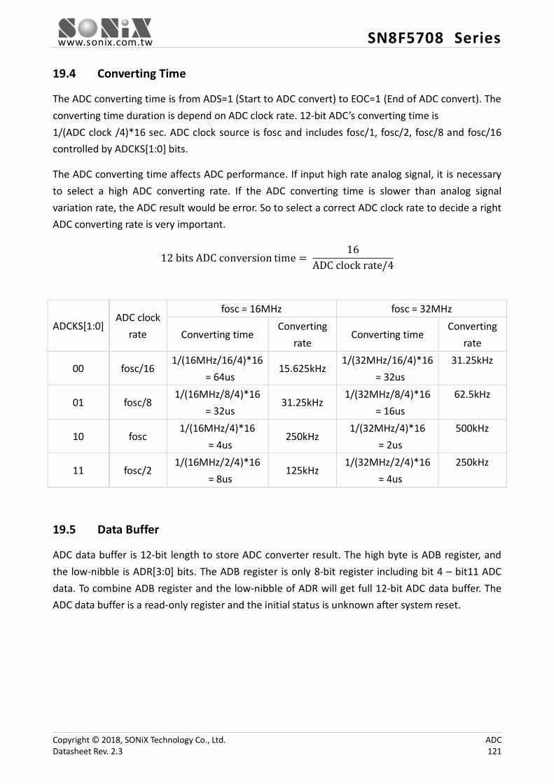
www.sonix.com.tw SN8F5708 Series
19.4 Converting Time
The ADC converting time is from ADS=1 (Start to ADC convert) to EOC=1 (End of ADC convert). The converting time duration is depend on ADC clock rate. 12-bit ADC’s converting time is 1/(ADC clock /4)*16 sec. ADC clock source is fosc and includes fosc/1, fosc/2, fosc/8 and fosc/16 controlled by ADCKS[1:0] bits.
The ADC converting time affects ADC performance. If input high rate analog signal, it is necessary to select a high ADC converting rate. If the ADC converting time is slower than analog signal variation rate, the ADC result would be error. So to select a correct ADC clock rate to decide a right ADC converting rate is very important.
12 bits ADC conversion time = 16
ADC clock rate/4
ADCKS[1:0] ADC clock
rate
fosc = 16MHz fosc = 32MHz
Converting time Converting
rate Converting time
Converting rate
00 fosc/16 1/(16MHz/16/4)*16
= 64us 15.625kHz
1/(32MHz/16/4)*16 = 32us
31.25kHz
01 fosc/8 1/(16MHz/8/4)*16
= 32us 31.25kHz
1/(32MHz/8/4)*16 = 16us
62.5kHz
10 fosc 1/(16MHz/4)*16
= 4us 250kHz
1/(32MHz/4)*16 = 2us
500kHz
11 fosc/2 1/(16MHz/2/4)*16
= 8us 125kHz
1/(32MHz/2/4)*16 = 4us
250kHz
19.5 Data Buffer
ADC data buffer is 12-bit length to store ADC converter result. The high byte is ADB register, and the low-nibble is ADR[3:0] bits. The ADB register is only 8-bit register including bit 4 – bit11 ADC data. To combine ADB register and the low-nibble of ADR will get full 12-bit ADC data buffer. The ADC data buffer is a read-only register and the initial status is unknown after system reset.
Copyright © 2018, SONiX Technology Co., Ltd. ADC Datasheet Rev. 2.3 121
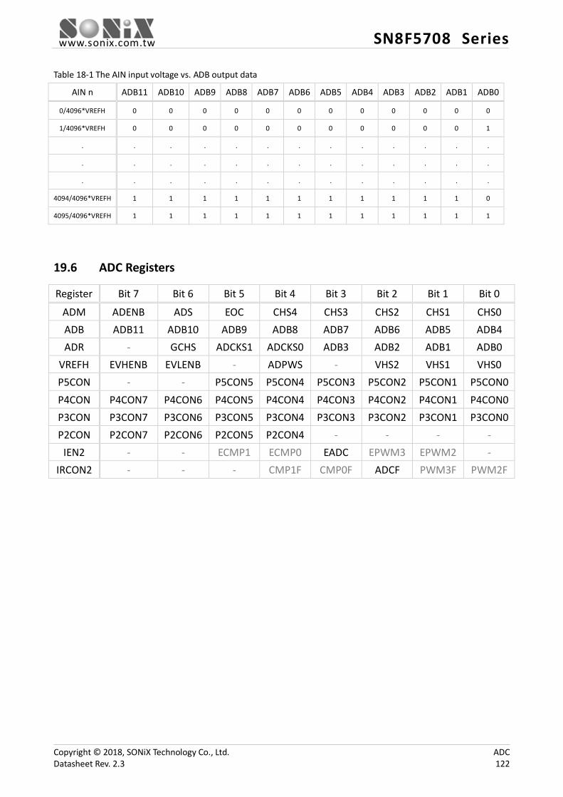
www.sonix.com.tw SN8F5708 Series
Table 18-1 The AIN input voltage vs. ADB output data
AIN n ADB11 ADB10 ADB9 ADB8 ADB7 ADB6 ADB5 ADB4 ADB3 ADB2 ADB1 ADB0
0/4096*VREFH 0 0 0 0 0 0 0 0 0 0 0 0
1/4096*VREFH 0 0 0 0 0 0 0 0 0 0 0 1
. . . . . . . . . . . . .
. . . . . . . . . . . . .
. . . . . . . . . . . . .
4094/4096*VREFH 1 1 1 1 1 1 1 1 1 1 1 0
4095/4096*VREFH 1 1 1 1 1 1 1 1 1 1 1 1
19.6 ADC Registers
Register Bit 7 Bit 6 Bit 5 Bit 4 Bit 3 Bit 2 Bit 1 Bit 0
ADM ADENB ADS EOC CHS4 CHS3 CHS2 CHS1 CHS0 ADB ADB11 ADB10 ADB9 ADB8 ADB7 ADB6 ADB5 ADB4 ADR - GCHS ADCKS1 ADCKS0 ADB3 ADB2 ADB1 ADB0
VREFH EVHENB EVLENB - ADPWS - VHS2 VHS1 VHS0 P5CON - - P5CON5 P5CON4 P5CON3 P5CON2 P5CON1 P5CON0 P4CON P4CON7 P4CON6 P4CON5 P4CON4 P4CON3 P4CON2 P4CON1 P4CON0 P3CON P3CON7 P3CON6 P3CON5 P3CON4 P3CON3 P3CON2 P3CON1 P3CON0 P2CON P2CON7 P2CON6 P2CON5 P2CON4 - - - -
IEN2 - - ECMP1 ECMP0 EADC EPWM3 EPWM2 - IRCON2 - - - CMP1F CMP0F ADCF PWM3F PWM2F
Copyright © 2018, SONiX Technology Co., Ltd. ADC Datasheet Rev. 2.3 122

www.sonix.com.tw SN8F5708 Series
ADM Register (0xD2) Bit Field Type Initial Description 7 ADENB R/W 0 ADC control bit. In stop mode, disable ADC to reduce
power consumption. 0: Disable 1: Enable
6 ADS R/W 0 ADC conversion control Write 1: Start ADC conversion (automatically cleared by the end of conversion)
5 EOC R/W 0 ADC status bit. 0: ADC progressing 1: End of conversion (automatically set by hardware; manually cleared by firmware)
4..0 CHS[4:0] R/W 0x00 ADC input channel select bit. 00000: AIN0, 00001: AIN1, 00010:AIN2, 00011: AIN3, 00100: AIN4,00101: AIN5, 00110: AIN6, 00111: AIN7, 01000: AIN8, 01001: AIN9, 01010:AIN10, 01011: AIN11, 11000: AIN12*(1), 11001: AIN13*(2), 11010: AIN14*(3), others: Reserved.
*(1) AIN12 channelis OP0-Amp output terminal.
*(2) AIN13 channelis OP1-Amp output terminal.
*(3) The AIN14 is internal 2V or 3V or 4V input channel.There is no any input pin from outside. In this time ADC
reference voltage must be internal VDD and External voltage, not internal 2V or 3V or 4V.
Copyright © 2018, SONiX Technology Co., Ltd. ADC Datasheet Rev. 2.3 123
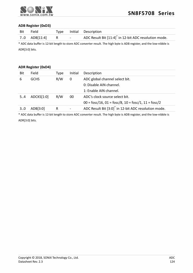
www.sonix.com.tw SN8F5708 Series
ADB Register (0xD3) Bit Field Type Initial Description 7..0 ADB[11:4] R - ADC Result Bit [11:4]* in 12-bit ADC resolution mode.
* ADC data buffer is 12-bit length to store ADC converter result. The high byte is ADB register, and the low-nibble is
ADR[3:0] bits.
ADR Register (0xD4) Bit Field Type Initial Description 6 GCHS R/W 0 ADC global channel select bit.
0: Disable AIN channel. 1: Enable AIN channel.
5..4 ADCKS[1:0] R/W 00 ADC’s clock source select bit. 00 = fosc/16, 01 = fosc/8, 10 = fosc/1, 11 = fosc/2
3..0 ADB[3:0] R - ADC Result Bit [3:0]* in 12-bit ADC resolution mode. * ADC data buffer is 12-bit length to store ADC converter result. The high byte is ADB register, and the low-nibble is
ADR[3:0] bits.
Copyright © 2018, SONiX Technology Co., Ltd. ADC Datasheet Rev. 2.3 124
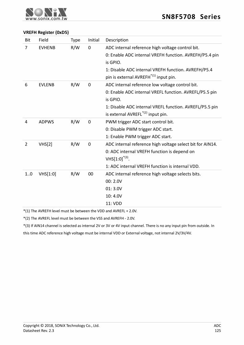
www.sonix.com.tw SN8F5708 Series
VREFH Register (0xD5) Bit Field Type Initial Description 7 EVHENB R/W 0 ADC internal reference high voltage control bit.
0: Enable ADC internal VREFH function. AVREFH/P5.4 pin is GPIO. 1: Disable ADC internal VREFH function. AVREFH/P5.4 pin is external AVREFH*(1) input pin.
6 EVLENB R/W 0 ADC internal reference low voltage control bit. 0: Enable ADC internal VREFL function. AVREFL/P5.5 pin is GPIO. 1: Disable ADC internal VREFL function. AVREFL/P5.5 pin is external AVREFL*(2) input pin.
4 ADPWS R/W 0 PWM trigger ADC start control bit. 0: Disable PWM trigger ADC start. 1: Enable PWM trigger ADC start.
2 VHS[2] R/W 0 ADC internal reference high voltage select bit for AIN14. 0: ADC internal VREFH function is depend on VHS[1:0]*(3). 1: ADC internal VREFH function is internal VDD.
1..0 VHS[1:0] R/W 00 ADC internal reference high voltage selects bits. 00: 2.0V 01: 3.0V 10: 4.0V 11: VDD
*(1) The AVREFH level must be between the VDD and AVREFL + 2.0V.
*(2) The AVREFL level must be between the VSS and AVREFH - 2.0V.
*(3) If AIN14 channel is selected as internal 2V or 3V or 4V input channel. There is no any input pin from outside. In
this time ADC reference high voltage must be internal VDD or External voltage, not internal 2V/3V/4V.
Copyright © 2018, SONiX Technology Co., Ltd. ADC Datasheet Rev. 2.3 125
www.sonix.com.tw SN8F5708 Series
P5CON Register (0xD7) Bit Field Type Initial Description 5..0 P5CON[5:0] R/W 0x00 P5 configuration control bit*.
0: P5 can be analog input pin (ADC input pin) or digital GPIO pin. 1: P5 is pure analog input pin and can’t be a digital GPIO pin.
* P5CON [5:0] will configure related Port5 pin as pure analog input pin to avoid current leakage.
P4CON Register (0xD6) Bit Field Type Initial Description 7..0 P4CON[7:0] R/W 0x00 P4 configuration control bit*.
0: P4 can be analog input pin (ADC input pin) or digital GPIO pin. 1: P4 is pure analog input pin and can’t be a digital GPIO pin.
* P4CON [7:0] will configure related Port4 pin as pure analog input pin to avoid current leakage.
P3CON Register (0x9F) Bit Field Type Initial Description 7..0 P3CON[7:0] R/W 0x00 P3 configuration control bit*.
0: P3 can be analog input pin (ADC input pin) or digital GPIO pin. 1: P3 is pure analog input pin and can’t be a digital GPIO pin.
* P3CON [7:0] will configure related Port3 pin as pure analog input pin to avoid current leakage.
Copyright © 2018, SONiX Technology Co., Ltd. ADC Datasheet Rev. 2.3 126
www.sonix.com.tw SN8F5708 Series
P2CON Register (0x9E) Bit Field Type Initial Description 7..4 P2CON[7:4] R/W 0x0 P2 configuration control bit*.
0: P2 can be analog input pin (ADC input pin) or digital GPIO pin. 1: P2 is pure analog input pin and can’t be a digital GPIO pin.
* P2CON [7:4] will configure related Port2 pin as pure analog input pin to avoid current leakage.
IEN2 Register (0x9A) Bit Field Type Initial Description 3 EADC R/W 0 ADC interrupt control bit.
0: Disable ADC interrupt function. 1: Enable ADC interrupt function.
Else Refer to other chapter(s) IRCON2 Register (0xBF) Bit Field Type Initial Description 2 ADCF R/W 0 ADC interrupt request flag.
0 = None ADC interrupt request. 1 = ADC interrupt request.
Else Refer to other chapter(s)
Copyright © 2018, SONiX Technology Co., Ltd. ADC Datasheet Rev. 2.3 127
www.sonix.com.tw SN8F5708 Series
19.7 Sample Code
The following sample code demonstrates how to perform ADC to convert AIN5 with interrupt.
1 2 3 4 5 6 7 8 9 10 11 12 13 14 15 16 17 18 19 20 21 22 23 24 25 26 27 28 29 30 31 32 33 34 35 36 37 38 39 40 41 42 43 44 45 46 47 48 49 50 51 52 53
#define ADCAIN14_VDD (3 << 0) //AIN14 = VDD #define ADCAIN14_4V (2 << 0) //AIN14 = 4.0V #define ADCAIN14_3V (1 << 0) //AIN14 = 3.0V #define ADCAIN14_2V (0 << 0) //AIN14 = 2.0V #define ADCInRefVDD (1 << 2) //internal reference from VDD #define ADCExLowRef (1 << 6) //low reference from AVREFL/P5.5 #define ADCExHighRef (1 << 7) //high reference from AVREFH/P5.4 #define ADCSpeedDiv16 (0 << 4) //ADC clock = fosc/16 #define ADCSpeedDiv8 (1 << 4) //ADC clock = fosc/8 #define ADCSpeedDiv1 (2 << 4) //ADC clock = fosc/1 #define ADCSpeedDiv2(3 << 4) //ADC clock = fosc/2 #define ADCChannelEn(1 << 6) //enable ADC channel #define SelAIN5 (5 << 0) //select ADC channel 5 #define ADCStart(1 << 6) //start ADC conversion #define ADCEn (1 << 7) //enable ADC #define EADC (1 << 3) //enable ADC interrupt #define ClearEOC 0xDF; unsigned int ADCBuffer; // data buffer void ADCInit(void) { P1 = 0x00; P1M = 0x80;
// set AIN5 pin's mode at pure analog pin P4CON |= 0x20; //AIN5/P45 P4M &= 0xDF; //input mode P4UR &= 0xDF; //disable pull-high
// configure ADC channel and enable ADC. ADM= ADCEn | SelAIN5; // enable channel and select conversion speed ADR= ADCChannelEn | ADCSpeedDiv1; // configure reference voltage VREFH = ADCExLowRef | ADCInRefVDD; // set external low reference pin's mode at pure analog pin P5CON |= 0x20; //AVREFL/P55 P5M&= 0xDF; //input mode P5UR&= 0xDF; //disable pull-high
// enable global interrupt IEN0 |= 0x80; //enable ADC interrupt IEN2 |= EADC;
// start ADC conversion ADM |= ADCStart;
}
Copyright © 2018, SONiX Technology Co., Ltd. ADC Datasheet Rev. 2.3 128
www.sonix.com.tw SN8F5708 Series
54 55 56 57 58 59 60 61 62 63 64
void ADCInterrupt(void) interrupt ISRAdc { if ((IRCON2 &0x04) == 0x04) {
P17= ~P17; IRCON2 &= 0xFB; //Clear ADCF ADCBuffer = (ADB << 4) + (ADR &0x0F); ADM&= ClearEOC; ADM|= ADCStart;
} }
Copyright © 2018, SONiX Technology Co., Ltd. ADC Datasheet Rev. 2.3 129
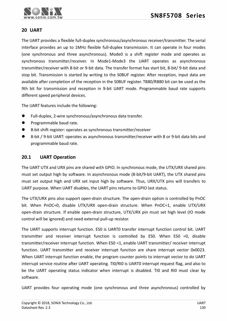
www.sonix.com.tw SN8F5708 Series
20 UART
The UART provides a flexible full-duplex synchronous/asynchronous receiver/transmitter. The serial interface provides an up to 1MHz flexible full-duplex transmission. It can operate in four modes (one synchronous and three asynchronous). Mode0 is a shift register mode and operates as synchronous transmitter/receiver. In Mode1-Mode3 the UART operates as asynchronous transmitter/receiver with 8-bit or 9-bit data. The transfer format has start bit, 8-bit/ 9-bit data and stop bit. Transmission is started by writing to the S0BUF register. After reception, input data are available after completion of the reception in the S0BUF register. TB80/RB80 bit can be used as the 9th bit for transmission and reception in 9-bit UART mode. Programmable baud rate supports different speed peripheral devices.
The UART features include the following:
Full-duplex, 2-wire synchronous/asynchronous data transfer. Programmable baud rate. 8-bit shift register: operates as synchronous transmitter/receiver 8-bit / 9-bit UART: operates as asynchronous transmitter/receiver with 8 or 9-bit data bits and
programmable baud rate.
20.1 UART Operation
The UART UTX and URX pins are shared with GPIO. In synchronous mode, the UTX/URX shared pins must set output high by software. In asynchronous mode (8-bit/9-bit UART), the UTX shared pins must set output high and URX set input high by software. Thus, URX/UTX pins will transfers to UART purpose. When UART disables, the UART pins returns to GPIO last status.
The UTX/URX pins also support open-drain structure. The open-drain option is controlled by PnOC bit. When PnOC=0, disable UTX/URX open-drain structure. When PnOC=1, enable UTX/URX open-drain structure. If enable open-drain structure, UTX/URX pin must set high level (IO mode control will be ignored) and need external pull-up resistor.
The UART supports interrupt function. ES0 is UART0 transfer interrupt function control bit. UART transmitter and receiver interrupt function is controlled by ES0. When ES0 =0, disable transmitter/receiver interrupt function. When ES0 =1, enable UART transmitter/ receiver interrupt function. UART transmitter and receiver interrupt function are share interrupt vector 0x0023. When UART interrupt function enable, the program counter points to interrupt vector to do UART interrupt service routine after UART operating. TI0/RI0 is UART0 interrupt request flag, and also to be the UART operating status indicator when interrupt is disabled. TI0 and RI0 must clear by software.
UART provides four operating mode (one synchronous and three asynchronous) controlled by
Copyright © 2018, SONiX Technology Co., Ltd. UART Datasheet Rev. 2.3 130

www.sonix.com.tw SN8F5708 Series
S0CON register. These modes can be support in different baud rate and communication protocols.
SM0 SM1 Mode Synchronization Clock Rate Start
Bit
Data
Bits
Stop
Bit
UART pins’ mode and
data
0 0 0 Synchronous Fcpu/12 X 8 X
UTX pin:
P00M=1 and P00=1
URX pin:
Transmitter:
P01M=1 and P01=1
Receiver:
P01M=0 and P01=1
0 1 1 Asynchronous Baud rate generator
or T1 overflow rate 1 8 1
UTX pin:
P00M=1 and P00=1
URX pin:
P01M=0 1 0 2 Asynchronous Fcpu/64 or Fcpu/32 1 9 1
1 1 3 Asynchronous Baud rate generator
or T1 overflow rate 1 9 1
20.2 Mode 0: Synchronous 8-bit Receiver/Transmitter
Mode0 is a shift register mode. It operates as synchronous transmitter/receiver. The UTX pin output shift clock for both transmit and receive condition. The URX pin is used to transmit and receive data. 8-bit data will be transmit and receive with LSB first. The baud rate is fcpu/12. Data transmission is started by writing data to S0BUF register. In the end of the 8th bit transmission, the TI0 flag is set. Data reception is controlled by REN0 bit and clearing RI0 bits. When REN0=1 and RI0 is from 1 to 0, data transmission starts and the RI0 flag is set at the end of the 8th bit reception.
20.3 Mode 1: 8-bit Receiver/Transmitter with Variable Baud Rate
Mode1 supports an asynchronous 8-bit UART with variable baud rate. The transfer format includes 1 start bit, 8 data bits (LSB first) and 1 stop bit. Data is transmitted by UTX pin and received by URX pin. The baud rate clock source can be baud rate generator or T1 overflow controlled by BD bit. When BD=0, the baud rate clock source is from T1 overflow. When BD=1, the baud rate clock source is from baud rate generator controlled by S0RELH and S0RELL. Additionally, the baud rate can be doubled by SMOD bit.
Data transmission is controlled by REN0 bit.After transmission configuration, load transmitted data into S0BUF, and then UART starts to transmit the pocket. The TI0 flag is set at the beginning of the
Copyright © 2018, SONiX Technology Co., Ltd. UART Datasheet Rev. 2.3 131
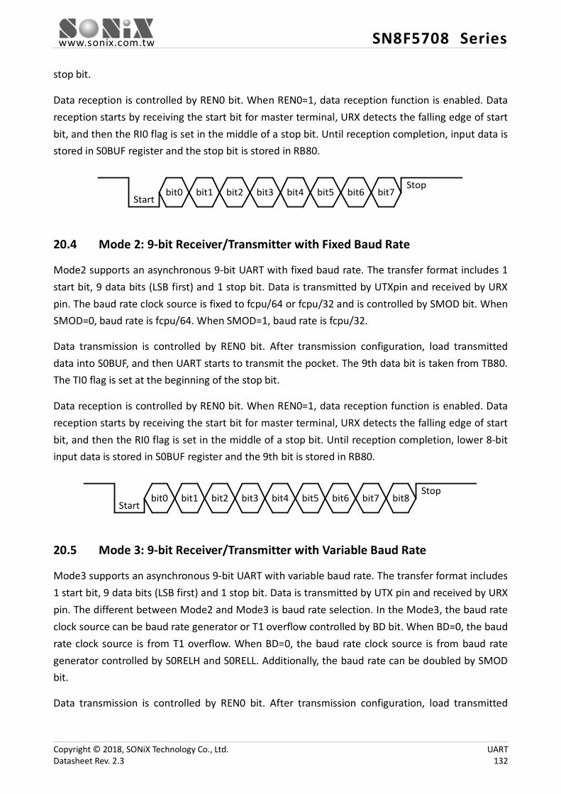
www.sonix.com.tw SN8F5708 Series
stop bit.
Data reception is controlled by REN0 bit. When REN0=1, data reception function is enabled. Data reception starts by receiving the start bit for master terminal, URX detects the falling edge of start bit, and then the RI0 flag is set in the middle of a stop bit. Until reception completion, input data is stored in S0BUF register and the stop bit is stored in RB80.
StartStop
bit0 bit1 bit2 bit3 bit4 bit5 bit6 bit7
20.4 Mode 2: 9-bit Receiver/Transmitter with Fixed Baud Rate
Mode2 supports an asynchronous 9-bit UART with fixed baud rate. The transfer format includes 1 start bit, 9 data bits (LSB first) and 1 stop bit. Data is transmitted by UTXpin and received by URX pin. The baud rate clock source is fixed to fcpu/64 or fcpu/32 and is controlled by SMOD bit. When SMOD=0, baud rate is fcpu/64. When SMOD=1, baud rate is fcpu/32.
Data transmission is controlled by REN0 bit. After transmission configuration, load transmitted data into S0BUF, and then UART starts to transmit the pocket. The 9th data bit is taken from TB80. The TI0 flag is set at the beginning of the stop bit.
Data reception is controlled by REN0 bit. When REN0=1, data reception function is enabled. Data reception starts by receiving the start bit for master terminal, URX detects the falling edge of start bit, and then the RI0 flag is set in the middle of a stop bit. Until reception completion, lower 8-bit input data is stored in S0BUF register and the 9th bit is stored in RB80.
StartStop
bit0 bit1 bit2 bit3 bit4 bit5 bit6 bit7 bit8
20.5 Mode 3: 9-bit Receiver/Transmitter with Variable Baud Rate
Mode3 supports an asynchronous 9-bit UART with variable baud rate. The transfer format includes 1 start bit, 9 data bits (LSB first) and 1 stop bit. Data is transmitted by UTX pin and received by URX pin. The different between Mode2 and Mode3 is baud rate selection. In the Mode3, the baud rate clock source can be baud rate generator or T1 overflow controlled by BD bit. When BD=0, the baud rate clock source is from T1 overflow. When BD=0, the baud rate clock source is from baud rate generator controlled by S0RELH and S0RELL. Additionally, the baud rate can be doubled by SMOD bit.
Data transmission is controlled by REN0 bit. After transmission configuration, load transmitted
Copyright © 2018, SONiX Technology Co., Ltd. UART Datasheet Rev. 2.3 132
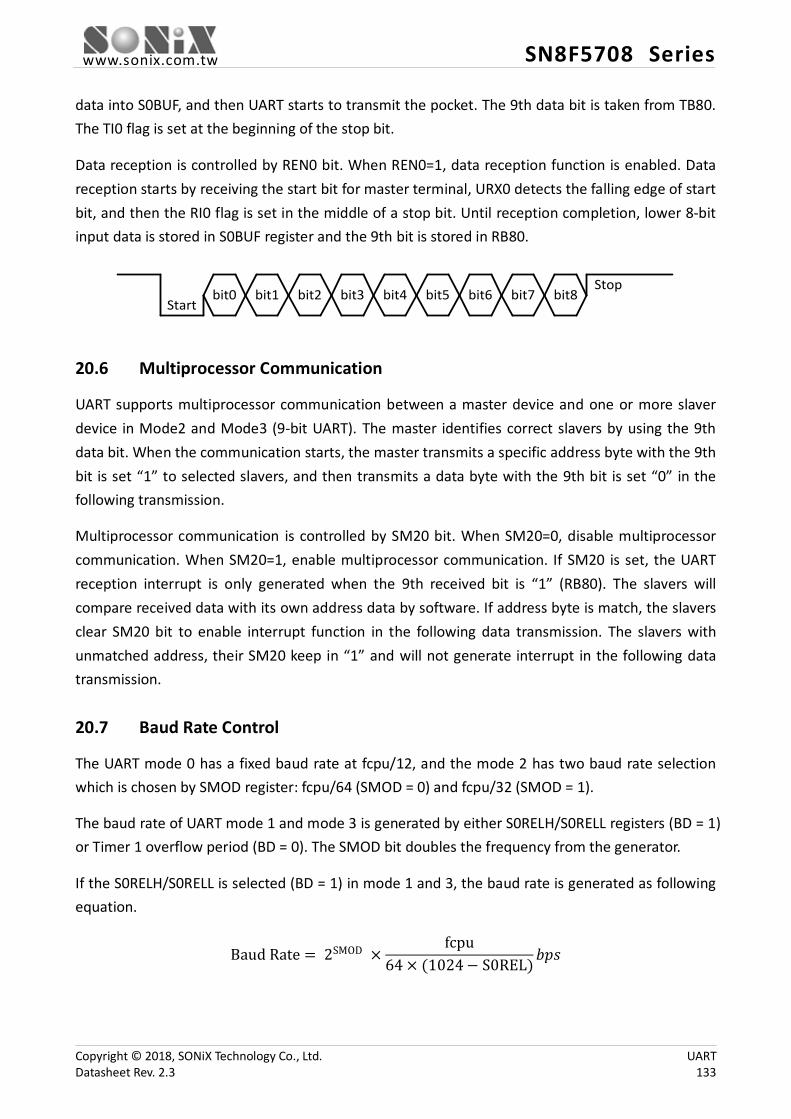
www.sonix.com.tw SN8F5708 Series
data into S0BUF, and then UART starts to transmit the pocket. The 9th data bit is taken from TB80. The TI0 flag is set at the beginning of the stop bit.
Data reception is controlled by REN0 bit. When REN0=1, data reception function is enabled. Data reception starts by receiving the start bit for master terminal, URX0 detects the falling edge of start bit, and then the RI0 flag is set in the middle of a stop bit. Until reception completion, lower 8-bit input data is stored in S0BUF register and the 9th bit is stored in RB80.
StartStop
bit0 bit1 bit2 bit3 bit4 bit5 bit6 bit7 bit8
20.6 Multiprocessor Communication
UART supports multiprocessor communication between a master device and one or more slaver device in Mode2 and Mode3 (9-bit UART). The master identifies correct slavers by using the 9th data bit. When the communication starts, the master transmits a specific address byte with the 9th bit is set “1” to selected slavers, and then transmits a data byte with the 9th bit is set “0” in the following transmission.
Multiprocessor communication is controlled by SM20 bit. When SM20=0, disable multiprocessor communication. When SM20=1, enable multiprocessor communication. If SM20 is set, the UART reception interrupt is only generated when the 9th received bit is “1” (RB80). The slavers will compare received data with its own address data by software. If address byte is match, the slavers clear SM20 bit to enable interrupt function in the following data transmission. The slavers with unmatched address, their SM20 keep in “1” and will not generate interrupt in the following data transmission.
20.7 Baud Rate Control
The UART mode 0 has a fixed baud rate at fcpu/12, and the mode 2 has two baud rate selection which is chosen by SMOD register: fcpu/64 (SMOD = 0) and fcpu/32 (SMOD = 1).
The baud rate of UART mode 1 and mode 3 is generated by either S0RELH/S0RELL registers (BD = 1) or Timer 1 overflow period (BD = 0). The SMOD bit doubles the frequency from the generator.
If the S0RELH/S0RELL is selected (BD = 1) in mode 1 and 3, the baud rate is generated as following equation.
Baud Rate = 2SMOD ×fcpu
64 × (1024− S0REL)𝑏𝑏𝑏𝑏𝑏𝑏
Copyright © 2018, SONiX Technology Co., Ltd. UART Datasheet Rev. 2.3 133
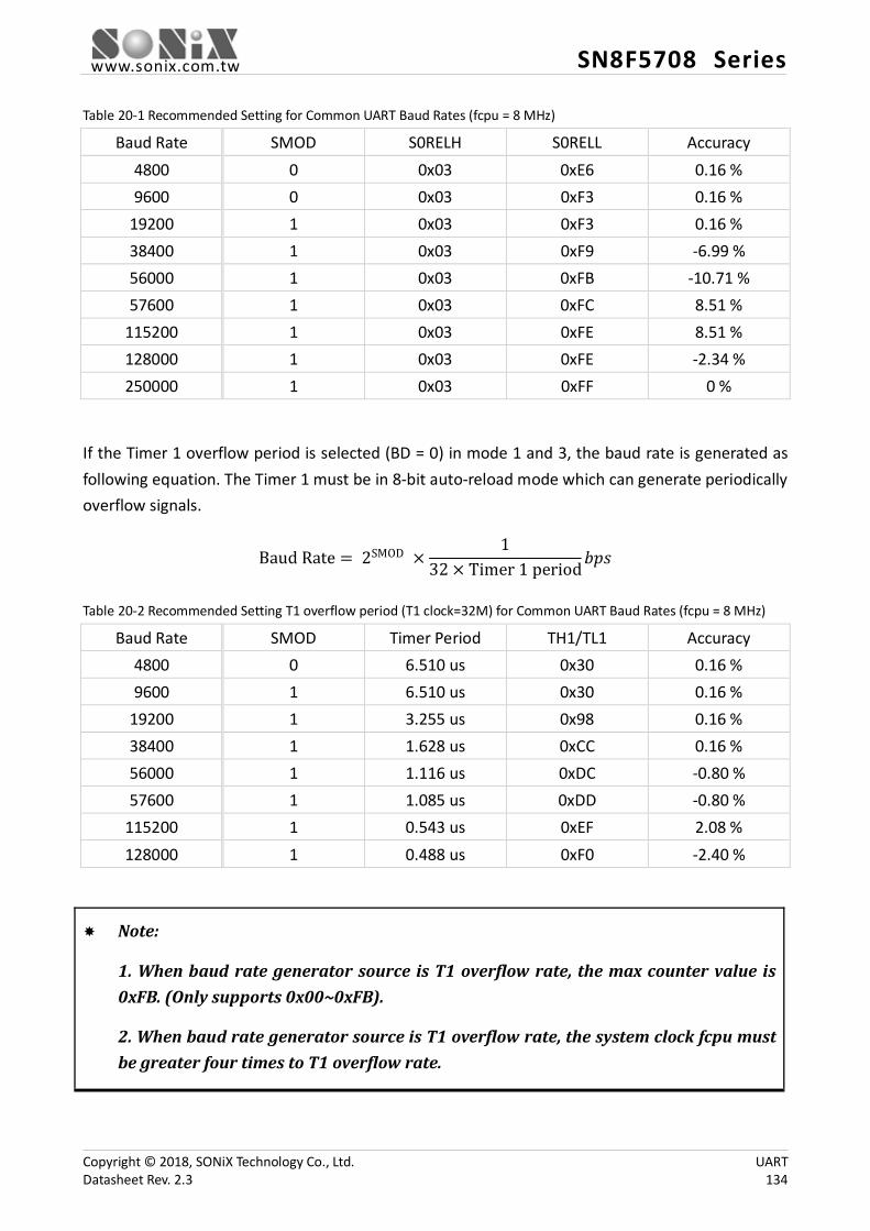
www.sonix.com.tw SN8F5708 Series
Table 20-1 Recommended Setting for Common UART Baud Rates (fcpu = 8 MHz)
Baud Rate SMOD S0RELH S0RELL Accuracy 4800 0 0x03 0xE6 0.16 % 9600 0 0x03 0xF3 0.16 %
19200 1 0x03 0xF3 0.16 % 38400 1 0x03 0xF9 -6.99 % 56000 1 0x03 0xFB -10.71 % 57600 1 0x03 0xFC 8.51 %
115200 1 0x03 0xFE 8.51 % 128000 1 0x03 0xFE -2.34 % 250000 1 0x03 0xFF 0 %
If the Timer 1 overflow period is selected (BD = 0) in mode 1 and 3, the baud rate is generated as following equation. The Timer 1 must be in 8-bit auto-reload mode which can generate periodically overflow signals.
Baud Rate = 2SMOD ×1
32 × Timer 1 period𝑏𝑏𝑏𝑏𝑏𝑏
Table 20-2 Recommended Setting T1 overflow period (T1 clock=32M) for Common UART Baud Rates (fcpu = 8 MHz)
Baud Rate SMOD Timer Period TH1/TL1 Accuracy 4800 0 6.510 us 0x30 0.16 % 9600 1 6.510 us 0x30 0.16 %
19200 1 3.255 us 0x98 0.16 % 38400 1 1.628 us 0xCC 0.16 % 56000 1 1.116 us 0xDC -0.80 % 57600 1 1.085 us 0xDD -0.80 %
115200 1 0.543 us 0xEF 2.08 % 128000 1 0.488 us 0xF0 -2.40 %
Note:
1. When baud rate generator source is T1 overflow rate, the max counter value is 0xFB. (Only supports 0x00~0xFB).
2. When baud rate generator source is T1 overflow rate, the system clock fcpu must be greater four times to T1 overflow rate.
Copyright © 2018, SONiX Technology Co., Ltd. UART Datasheet Rev. 2.3 134

www.sonix.com.tw SN8F5708 Series
20.8 UART Registers
Register Bit 7 Bit 6 Bit 5 Bit 4 Bit 3 Bit 2 Bit 1 Bit 0
S0CON SM0 SM1 SM20 REN0 TB80 RB80 TI0 RI0 S0CON2 BD - - - - - - - S0BUF S0BUF7 S0BUF6 S0BUF5 S0BUF4 S0BUF3 S0BUF2 S0BUF1 S0BUF0 PCON SMOD - - - P2SEL GF0 STOP IDLE
S0RELH - - - - - - S0REL9 S0REL8 S0RELL S0REL7 S0REL6 S0REL5 S0REL4 S0REL3 S0REL2 S0REL1 R0REL0
IEN0 EAL - ET2 ES0 ET1 EX1 ET0 EX0 P1OC PW3EN PW2EN PW1EN P06OC P05OC P13OC P12OC P11OC P0M P07M P06M P05M P04M P03M P02M P01M P00M P0 P07 P06 P05 P04 P03 P02 P01 P00
S0CONRegister (0x98) Bit Field Type Initial Description 7..6 SM[0:1] R/W 00 UART mode selection
00: Mode 0 01: Mode 1 10: Mode 2 11: Mode 3
5 SM20 R/W 0 Multiprocessor communication (mode 2, 3) 0: Disable 1: Enable
4 REN0 R/W 0 UART reception function 0: Disable 1: Enable
3 TB80 R/W 0 The 9th bit transmission data (mode 2, 3) 2 RB80 R/W 0 The 9th bit data from reception 1 TI0 R/W 0 UART interrupt flag of transmission 0 RI0 R/W 0 UART interrupt flag of reception
Note: TI0 and RI0 are clear by software when interrupt is enabled.
Copyright © 2018, SONiX Technology Co., Ltd. UART Datasheet Rev. 2.3 135
www.sonix.com.tw SN8F5708 Series
S0CON2 Register (0xD8) Bit Field Type Initial Description 7 BD R/W 0 Baud rate generators selection (mode 1, 3)
0: Timer 1 overflow period 1: Controlled by S0RELH, S0RELL registers
6..0 Reserved R 0x00 S0BUF Register (0x99) Bit Field Type Initial Description 7..0 S0BUF R/W 0x00 Action of writing data triggers UART communication (LSB
first). Reception data is available to read by the end of packages.
PCON Register (0x87) Bit Field Type Initial Description 7 SMOD R/W 0 UART baud rate control (UART mode 0, 2)
0: fcpu/64 1: fcpu/32
6..0 Refer to other chapter(s) S0RELH/S0RELL Registers (S0RELH: 0xBA, S0RELL: 0xAA) Bit Field Type Initial Description 15..10 Reserved R 0x00 9..0 S0REL[9:0] R/W 0x00 S0RELH[1:0] &S0RELL[7:0]. UART Reload Register is used
for UART baud rate generation. IEN0 Register (0xA8) Bit Field Type Initial Description 7 EAL R/W 0 Interrupts enable. Refer to Chapter Interrupt 4 ES0 R/W 0 Enable UART interrupt Else Refer to other chapter(s)
Copyright © 2018, SONiX Technology Co., Ltd. UART Datasheet Rev. 2.3 136

www.sonix.com.tw SN8F5708 Series
P1OC Register (0xE4) Bit Field Type Initial Description 4 P06OC R/W 0 0: Switch P0.6 (URX) to input mode (required)
1: Switch P0.6 (URX) to open-drain mode* 3 P05OC R/W 0 0: Switch P0.5 (UTX) to push-pull mode
1: Switch P0.5 (UTX) to open-drain mode Else Refer to other chapter(s)
* Setting P06OC as high causes URX cannot receive data.
P0M Register (0xF9) Bit Field Type Initial Description 6 P06M R/W 0 0: Set P0.6 (URX) as input mode (required)
1: Set P0.6 (URX) as output mode*
5 P05M R/W 0 0: Set P0.5 (UTX) as input mode*
1: Set P0.5 (UTX) as output mode (required) Else Refer to other chapter(s)
* The URX and UTX respectively require input and output mode selection to receive/transmit data appropriately.
P0 Register (0x80) Bit Field Type Initial Description 6 P06 R/W 0 This bit is available to read at any time for monitoring
the bus statue. 5 P05 R/W 0 0: Set P0.5 (UTX) always low*
1: Make P0.5 (UTX) can output UART data (required) Else Refer to other chapter(s)
* Setting P05 initially high because UART block drive the shared pin low signal only.
Copyright © 2018, SONiX Technology Co., Ltd. UART Datasheet Rev. 2.3 137
www.sonix.com.tw SN8F5708 Series
20.9 Sample Code
The following sample code demonstrates how to perform UART mode 1 with interrupt.
1 2 3 4 5 6 7 8 9 10 11 12 13 14 15 16 17 18 19 20 21 22 23 24 25 26 27 28 29 30 31 32 33 34 35 36 37 38 39 40
#define SYSUartSM0 (0<< 6) #define SYSUartSM1 (1 << 6) #define SYSUartSM2 (2 << 6) #define SYSUartSM3 (3 << 6) #define SYSUartREN (1 << 4) #define SYSUartSMOD (1 << 7) #define SYSUartES0 (1 << 4) void SYSUartInit(void) { // set UTX, URX pins’ mode at here or at GPIO initialization P05 = 1; P0M = P0M | 0x20& ~0x40; // configure UART mode between SM0 and SM3, enable URX S0CON = SYSUartSM1 | SYSUartREN; // configure UART baud rate PCON = SYSUartSMODE1; S0CON2 = SYSUartBD1; S0RELH = 0x03; S0RELL = 0xFE; // enable UART interrupt IEN0 |= SYSUartES0; // send first UTX data S0BUF = uartTxBuf; } void SYSUartInterrupt(void) interrupt ISRUart { if (TI0 == 1) { S0BUF = uartTxBuf; TI0 = 0; } else if (RI0 == 1) {
uartRxBuf = S0BUF; RI0 = 0; }
}
Copyright © 2018, SONiX Technology Co., Ltd. UART Datasheet Rev. 2.3 138
www.sonix.com.tw SN8F5708 Series
21 SPI
The SPI a serial communicate interface for data exchanging from one MCU to one MCU or other hardware peripherals. It is a simple 8-bit interface without a major definition of protocol, packet or control bits. The SPI transceiver includes three pins, clock (SCK), data input and data output (MISO/ MOSI) to send data between master and slaver terminals. An optional slave select pin (SSN) can be enabled by register in slave mode. The SPI interface builds in 4-mode which are the clock idle status and the clock phases.
Full-duplex, 3-wire synchronous data transfer. Master (SCK is clock output) or Slave (SCK is clock input) operation. Seven SPI Master baud rates. Slave Clock rate up to fcpu/8. 8-bit data transmitted MSB first, LSB last. Serial clock with programmable polarity and phase. Master Mode fault error flag with MCU interrupt capability. Write collision flag protection.
21.1 SPI Operation
The SPCON register can control SPI operating function, such as: transmit/receive, clock rate, data transfer direction, SPI clock idle status and clock control phase and enable this circuit. This SPI circuit will transmit or receive 8-bit data automatically by setting SPEN in SPCON register and write or read SPDAT register.
CPOL bit is designed to control SPI clock idle status. CPHA bit is designed to control the clock edge direction of data receive. CPOL and CPHA bits decide the SPI format. The SPI data transfer direction is MSB bit to LSB bit.
The SPI supports 4-mode format controlled by CPOL and CPHA bits. The edge direction is “Data Transfer Edge”. When setting rising edge that means to receive and transmit one bit data at SCK rising edge, and data transition is at SCK falling edge. When setting falling edge, that means to receive and transmit one bit data at SCK falling edge, and data transition is at SCK rising edge.
“CPHA” is the clock phase bit controls the phase of the clock on which data is sampled. When CPHA=1, the SCK first edge is for data transition, and receive and transmit data is at SCK 2nd edge. When CPHA=0, the 1st bit is fixed already, and the SCK first edge is to receive and transmit data. The SPI data transfer timing as following figure:
Copyright © 2018, SONiX Technology Co., Ltd. SPI Datasheet Rev. 2.3 139

www.sonix.com.tw SN8F5708 Series
C P O L
C P H A
Diagrams Description
0 1 bit5 bit4 bit3 bit2 bit1bit6bit7 bit0
SCK idle status = Low. The transfer first bit = MSB. SCK data transfer edge = Falling edge.
1 1 bit5 bit4 bit3 bit2 bit1bit6bit7 bit0
SCK idle status = High. The transfer first bit = MSB. SCK data transfer edge = Rising edge.
0 0 bit5 bit4 bit3 bit2 bit1bit6bit7 bit0 Next data
SCK idle status = Low. The transfer first bit = MSB. SCK data transfer edge = Rising edge.
1 0 bit5 bit4 bit3 bit2 bit1bit6bit7 bit0 Next data
SCK idle status = High. The transfer first bit = MSB. SCK data transfer edge = Falling edge.
The SPI supports interrupt function. ESPI is SPI interrupt function control bit. ESPI=0, disable SPI interrupt function. ESPI=1, enable SPI interrupt function. When SPI interrupt function enable, the program counter points to interrupt vector to do SPI interrupt service routine after SPI operating. SPIF is SPI interrupt request flag, and also to be the SPI operating status indicator when ESPI= 0, but cleared by reading the SPSTA,SPDAT registers.
SPI builds in chip selection function to implement SPI multi-device mode. One master communicating with several slave devices in SPI bus, and the chip selection decides the pointed device. The chip selection pin is SSN pin.
The SPI pins also support open-drain structure. The open-drain option is controlled by PnOC bits. When PnOC=0, disable SPI open-drain structure. When PnOC=1, enable SPI open-drain structure. If enable open-drain structure, SPI pins must be set input mode and need external pull-up resistor.
Copyright © 2018, SONiX Technology Co., Ltd. SPI Datasheet Rev. 2.3 140
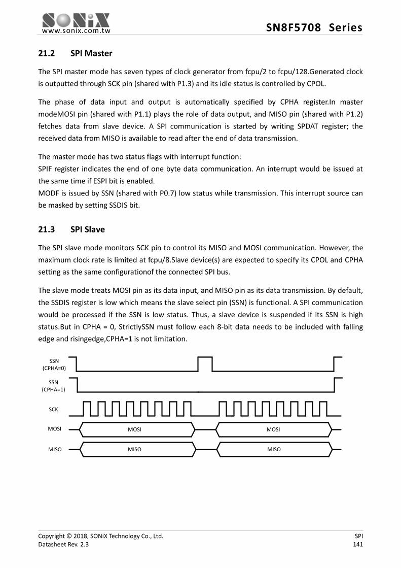
www.sonix.com.tw SN8F5708 Series
21.2 SPI Master
The SPI master mode has seven types of clock generator from fcpu/2 to fcpu/128.Generated clock is outputted through SCK pin (shared with P1.3) and its idle status is controlled by CPOL.
The phase of data input and output is automatically specified by CPHA register.In master modeMOSI pin (shared with P1.1) plays the role of data output, and MISO pin (shared with P1.2) fetches data from slave device. A SPI communication is started by writing SPDAT register; the received data from MISO is available to read after the end of data transmission.
The master mode has two status flags with interrupt function: SPIF register indicates the end of one byte data communication. An interrupt would be issued at the same time if ESPI bit is enabled. MODF is issued by SSN (shared with P0.7) low status while transmission. This interrupt source can be masked by setting SSDIS bit.
21.3 SPI Slave
The SPI slave mode monitors SCK pin to control its MISO and MOSI communication. However, the maximum clock rate is limited at fcpu/8.Slave device(s) are expected to specify its CPOL and CPHA setting as the same configurationof the connected SPI bus.
The slave mode treats MOSI pin as its data input, and MISO pin as its data transmission. By default, the SSDIS register is low which means the slave select pin (SSN) is functional. A SPI communication would be processed if the SSN is low status. Thus, a slave device is suspended if its SSN is high status.But in CPHA = 0, StrictlySSN must follow each 8-bit data needs to be included with falling edge and risingedge,CPHA=1 is not limitation.
MOSI
MISO
MOSI
MISO
SSN(CPHA=1)
SSN(CPHA=0)
SCK
MOSI
MISO
Copyright © 2018, SONiX Technology Co., Ltd. SPI Datasheet Rev. 2.3 141
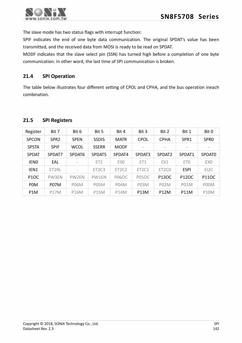
www.sonix.com.tw SN8F5708 Series
The slave mode has two status flags with interrupt function: SPIF indicates the end of one byte data communication. The original SPDAT’s value has been transmitted, and the received data from MOSI is ready to be read on SPDAT. MODF indicates that the slave select pin (SSN) has turned high before a completion of one byte communication. In other word, the last time of SPI communication is broken.
21.4 SPI Operation
The table below illustrates four different setting of CPOL and CPHA, and the bus operation ineach combination.
21.5 SPI Registers
Register Bit 7 Bit 6 Bit 5 Bit 4 Bit 3 Bit 2 Bit 1 Bit 0
SPCON SPR2 SPEN SSDIS MATR CPOL CPHA SPR1 SPR0 SPSTA SPIF WCOL SSERR MODF - - - - SPDAT SPDAT7 SPDAT6 SPDAT5 SPDAT4 SPDAT3 SPDAT2 SPDAT1 SPDAT0 IEN0 EAL - ET2 ES0 ET1 EX1 ET0 EX0 IEN1 ET2RL - ET2C3 ET2C2 ET2C1 ET2C0 ESPI EI2C P1OC PW3EN PW2EN PW1EN P06OC P05OC P13OC P12OC P11OC P0M P07M P06M P05M P04M P03M P02M P01M P00M P1M P17M P16M P15M P14M P13M P12M P11M P10M
Copyright © 2018, SONiX Technology Co., Ltd. SPI Datasheet Rev. 2.3 142
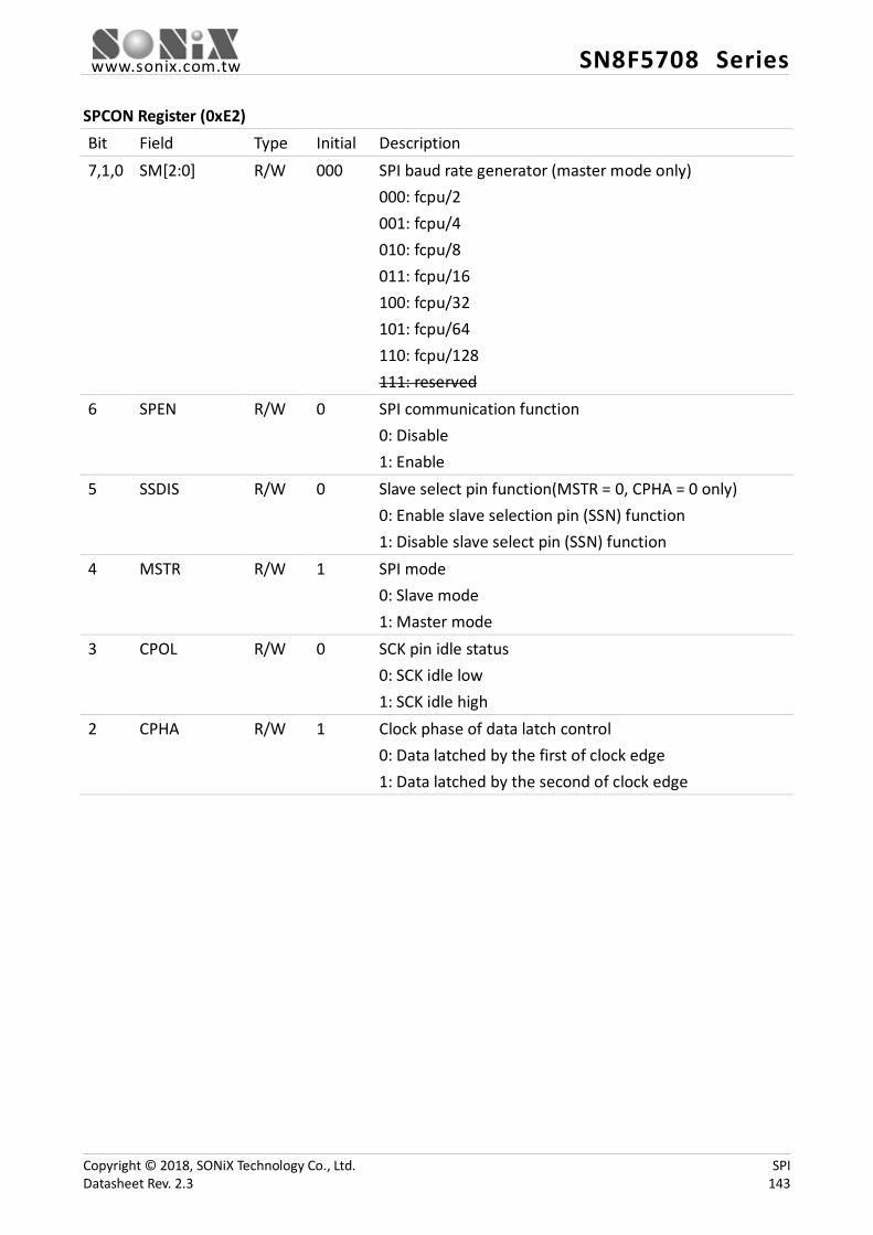
www.sonix.com.tw SN8F5708 Series
SPCON Register (0xE2) Bit Field Type Initial Description 7,1,0 SM[2:0] R/W 000 SPI baud rate generator (master mode only)
000: fcpu/2 001: fcpu/4 010: fcpu/8 011: fcpu/16 100: fcpu/32 101: fcpu/64 110: fcpu/128 111: reserved
6 SPEN R/W 0 SPI communication function 0: Disable 1: Enable
5 SSDIS R/W 0 Slave select pin function(MSTR = 0, CPHA = 0 only) 0: Enable slave selection pin (SSN) function 1: Disable slave select pin (SSN) function
4 MSTR R/W 1 SPI mode 0: Slave mode 1: Master mode
3 CPOL R/W 0 SCK pin idle status 0: SCK idle low 1: SCK idle high
2 CPHA R/W 1 Clock phase of data latch control 0: Data latched by the first of clock edge 1: Data latched by the second of clock edge
Copyright © 2018, SONiX Technology Co., Ltd. SPI Datasheet Rev. 2.3 143

www.sonix.com.tw SN8F5708 Series
SPSTA Register (0xE1) Bit Field Type Initial Description 7 SPIF R 0 SPI complete communication flag
Set automatically at the end of communication Cleared automatically by reading SPSTA, SPDAT registers
6 WCOL R 0 Write collision flag Set automatically if write SPDATduring communication Cleared automatically by reading SPSTA, SPDAT registers
5 SSERR R 0 Synchronous slave select pin error Set automatically if SSN error controlling Cleared automatically by clear SPEN
4 MODF R 0 Mode fault flag 3..0 Reserved R 0x00
SPDAT Register (0xE3) Bit Field Type Initial Description 7..0 SPDAT R/W 0x00 Master mode: action of writing data triggers SPI
communication; reception data is readable after the end of one byte communication (SPIF automatically set). Slave mode: written data would be transmitted by SCK input; reception data is available to read after the end of one byte communication (SPIF automatically set).
IEN0 Register (0xA8) Bit Field Type Initial Description 7 EAL R/W 0 Interrupts enable. Refer to Chapter Interrupt Else Refer to other chapter(s)
IEN1 Register (0xB8) Bit Field Type Initial Description 1 ESPI R/W 0 Enable SPI interrupt Else Refer to other chapter(s)
Copyright © 2018, SONiX Technology Co., Ltd. SPI Datasheet Rev. 2.3 144

www.sonix.com.tw SN8F5708 Series
P1OC Register (0xE4) Bit Field Type Initial Description 2 P13OC R/W 0 0: Switch P1.3 (SCK) to input or output mode
1: Switch P1.3 (SCK) to open-drain mod 1 P12OC R/W 0 0: Switch P1.2 (MISO) to input or output mode
1: Switch P1.2 (MISO) to open-drain mod 0 P11OC R/W 0 0: Switch P1.1 (MOSI) to input or output mode
1: Switch P1.1 (MOSI) to open-drain mode Else Refer to other chapter(s)
P0M Register (0xF9) Bit Field Type Initial Description 7 P07M R/W 0 0: Set P0.7 (SSN) as input mode*
1: Set P0.7 (SSN) as output mode* Else Refer to other chapter(s)
*If slave mode with SSN function: essentially to set SSN as input mode.
P1M Register Bit Field Type Initial Description 3 P13M R/W 0 0: Set P1.3 (SCK) as input modeslave mode
1: Set P1.3 (SCK) as output modemaster mode 2 P12M R/W 0 0: Set P1.2 (MISO) as input modemaster mode
1: Set P1.2 (MISO) as output modeslave mode 1 P11M R/W 0 0: Set P1.1 (MOSI) as input modeslave mode
1: Set P1.1 (MOSI) as output modemaster mode Else Refer to other chapter(s)
1Setting SCK as input mode is essential in slave mode; setting as output mode is recommended in master mode. 2Setting MISO as input mode is essential in master mode; setting as output mode is recommended in slave mode. 3Setting MOSI as input mode is essential is slave mode; setting as output mode is recommended in master mode.
Copyright © 2018, SONiX Technology Co., Ltd. SPI Datasheet Rev. 2.3 145

www.sonix.com.tw SN8F5708 Series
21.6 Sample Code
The following sample code demonstrates how to perform SPI Master with interrupt.
1 2 3 4 5 6 7 8 9 10 11 12 13 14 15 16 17 18 19 20 21 22 23 24 25 26 27 28 29 30 31 32 33 34 35 36 37 38 39 40 41 42 43 44 45 46 47 48 49 50 51 52
#define SpiMaster (1<<4) //SPI = Master mode #define SpiSlave (1<<4) //SPI = Slave mode #define SpiMode0 (0<<2) //SCK idle low, data latch at rising edge #define SpiMode1 (1<<2) //SCK idle low, data latch at falling edge #define SpiMode2 (2<<2) //SCK idle high, data latch at falling edge #define SpiMode3 (3<<2) //SCK idle high, data latch at rising edge #define SpiEn (1<<6) //Enable SPI #define SpiSSNEn (0<<5) //SSN pin function enable #define SpiSSNDis (1<<5) //SSN pin function disable unsigned charu8SpiData = 0; // data buffer unsigned char u8TxCompleted = 0; void SpiMaster(void) { unsigned char u8RcvData = 0;
//SCK & MOSI = output, MISO = input P1M |= 0x0A; //Enable Spi, Master mode, SSN pin disable, Fclk/128 //SCK idle low, data latch at falling edge SPCON = SpiEn | SpiMaster | SpiMode1 | SpiSSNDis | 0x82; //Enable Global/SPI interrupt IEN1 |= 0x02; IEN0 |= 0x80; //enable global interrupt
while (1) { SPDAT= 0x55; while(!u8TxCompleted); // wait end of transmition u8TxCompleted = 0; // clear sw flag u8RcvData = u8SpiData; // receive 0x66 SPDAT=0x99; while(!u8TxCompleted); // wait end of transmition u8TxCompleted = 0; // clear sw flag u8RcvData = u8SpiData; // receive 0xAA } } void SpiInterrupt(void) interrupt ISRSpi //0x4B { switch ( SPSTA ) // Clear SPI flag (SPIF) by reading { case 0x80: u8SpiData = SPDAT; u8TxCompleted = 1; break; case 0x10: // Mode Fault break; } }
Copyright © 2018, SONiX Technology Co., Ltd. SPI Datasheet Rev. 2.3 146

www.sonix.com.tw SN8F5708 Series
22 I2C
The I2C is a serial communication interface for data exchanging from one MCU to one MCU or other hardware peripherals. The device can transmit data as a master or a slave with two bi-directional IO, SDA (Serial data output) and SCL (Serial clock input).
When a master transmit data to a slave, it’s called “WRITE” operation; when a slave transmit data to a master, it’s called “READ” operation. It also supports multi-master communication and keeps data transmission correctly by an arbitration method to decide one master has the control on bus and transmit its data.
Master Tx,Rx Mode Slave Tx,Rx mode (with general address call) for multiplex slave in single master situation. 2-wire synchronous data transfer/receiver. Support 100K/400K clock rate.
22.1 I2C Protocol
I2C transmission structure includes a START(S) condition, 8-bit address byte, one or more data byte and a STOP (P) condition. START condition is generated by master to initial any transmission.
Data is transmitted with the Most Significant Bit (MSB) first. In address byte, the higher 7-bit is address bit and the lowest bit is data direction (R/W) bit. When R/W=0, it assigns a “WRITR” operation. When R/W=1, it assigns a “READ” operation.
After each byte is received, the receiver (a master or a slave) must send an acknowledge (ACK). If transmitter can’t receive an ACK, it will recognize a not acknowledge (NACK). In WRITE operation, the master will transmit data to the slave and then waits for ACK from slave. In READ operation, the slave will transmit data to the master and then waits for ACK from master. In the end, the master will generate a STOP condition to finish transmission.
S
Transmit Address
ACK
1
A7
2
A6
3
A5
4
A4
5
A3
6
A2
7
A1
8 9 1 2
D6
3
D5
4
D4
5
D3
6
D2
7
D1
8
D0
9 P
SDA
SCL
Transmission Data
R/W D7
Ack signal from receiver
SCL held low,while interrupt executing
NACK
Nack signal from receiver
START Condition STOP Condition
Copyright © 2018, SONiX Technology Co., Ltd. I2C Datasheet Rev. 2.3 147
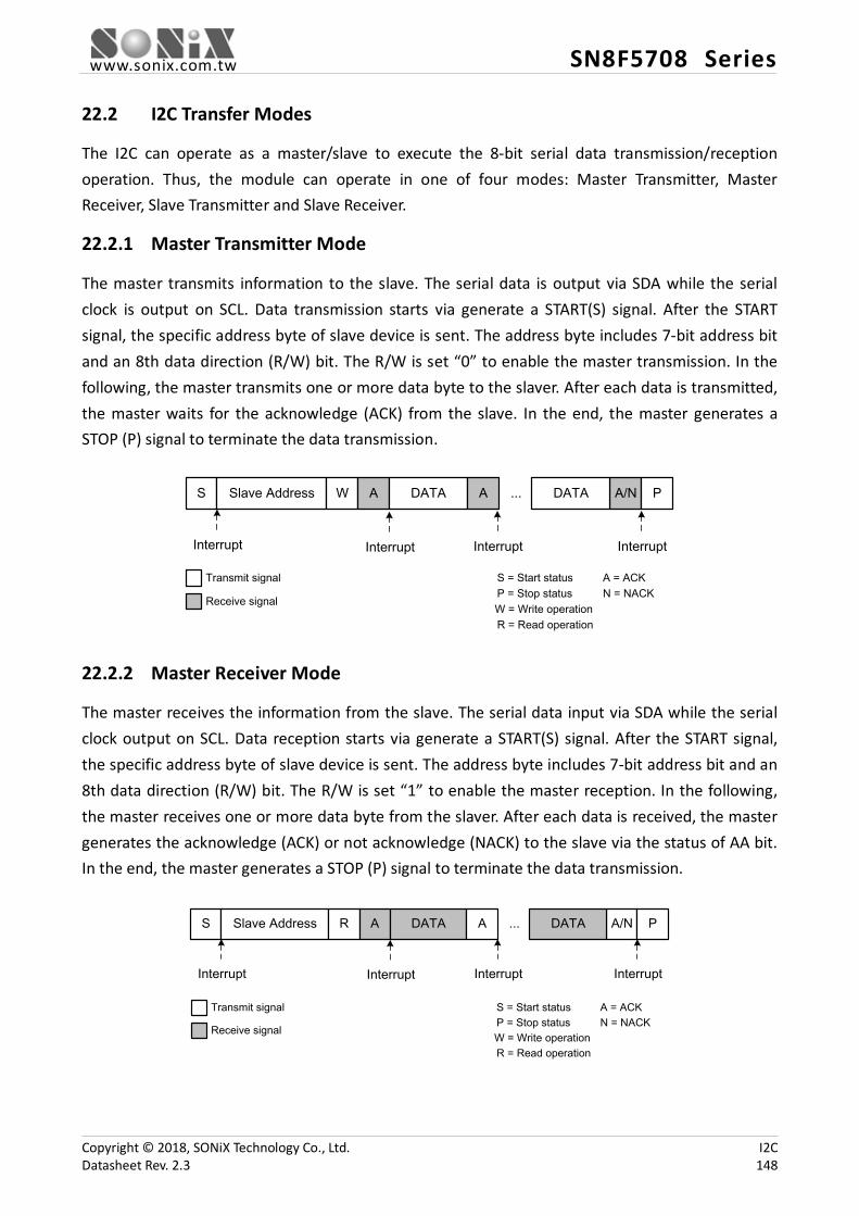
www.sonix.com.tw SN8F5708 Series
22.2 I2C Transfer Modes
The I2C can operate as a master/slave to execute the 8-bit serial data transmission/reception operation. Thus, the module can operate in one of four modes: Master Transmitter, Master Receiver, Slave Transmitter and Slave Receiver.
22.2.1 Master Transmitter Mode
The master transmits information to the slave. The serial data is output via SDA while the serial clock is output on SCL. Data transmission starts via generate a START(S) signal. After the START signal, the specific address byte of slave device is sent. The address byte includes 7-bit address bit and an 8th data direction (R/W) bit. The R/W is set “0” to enable the master transmission. In the following, the master transmits one or more data byte to the slaver. After each data is transmitted, the master waits for the acknowledge (ACK) from the slave. In the end, the master generates a STOP (P) signal to terminate the data transmission.
S Slave Address W A DATA A A/N P... DATA
Transmit signal
Receive signal
S = Start statusP = Stop status
A = ACKN = NACK
W = Write operationR = Read operation
Interrupt Interrupt Interrupt Interrupt
22.2.2 Master Receiver Mode
The master receives the information from the slave. The serial data input via SDA while the serial clock output on SCL. Data reception starts via generate a START(S) signal. After the START signal, the specific address byte of slave device is sent. The address byte includes 7-bit address bit and an 8th data direction (R/W) bit. The R/W is set “1” to enable the master reception. In the following, the master receives one or more data byte from the slaver. After each data is received, the master generates the acknowledge (ACK) or not acknowledge (NACK) to the slave via the status of AA bit. In the end, the master generates a STOP (P) signal to terminate the data transmission.
S Slave Address R A DATA A A/N P... DATA
Transmit signal
Receive signal
S = Start statusP = Stop status
A = ACKN = NACK
W = Write operationR = Read operation
Interrupt Interrupt Interrupt Interrupt
Copyright © 2018, SONiX Technology Co., Ltd. I2C Datasheet Rev. 2.3 148

www.sonix.com.tw SN8F5708 Series
22.2.3 Slave Transmitter Mode
The slave transmits information to the master. The serial data output via SDA while the serial clock input on SCL. Data transmission starts via receive a START(S) signal from the master. After the START signal, the specific address byte of slave device is received. The address byte includes 7-bit address bit and an 8th data direction (R/W) bit. The R/W is set “1” to enable the slave transmission. If the received address byte match the address in I2CADR register, the slave generate an acknowledge (ACK). Otherwise, if general call address condition is set (GC=1), the slave also generate an acknowledge (ACK) after general call address (0x00) is received. In the following, the slave transmits one or more data byte to the master. After each data is transmitted, the slave waits for the acknowledge (ACK) from the master. In the end, the slave receives a STOP (P) signal from the master to terminate the data transmission.
S Slave Address R A DATA A A/N P... DATA
Transmit signal
Receive signal
S = Start statusP = Stop status
A = ACKN = NACK
W = Write operationR = Read operation
Interrupt
Interrupt Interrupt Interrupt
22.2.4 Slave Receiver Mode
The slave receives information from the master. Both the serial data and the serial clock are input on SDA and SCL. Data reception starts via receive a START(S) signal from the master. After the START signal, the specific address byte of slave device is received. The address byte includes 7-bit address bit and an 8th data direction (R/W) bit. The R/W is set “0” to enable the slave reception. If the received address byte match the address in I2CADR register, the slave generate an acknowledge (ACK). Otherwise, if general call address condition is set (GC=1), the slave also generate an acknowledge (ACK) after general call address (0x00) is received. In the following, the slave receives one or more data byte from the master. After each data is receives, the slave generates the acknowledge (ACK) or not acknowledge (NACK) to the master via the status of AA bit. In the end, the slave receives a STOP (P) signal from the master to terminate the data transmission.
S Slave Address W A DATA A A/N P... DATA
Transmit signal
Receive signal
S = Start statusP = Stop status
A = ACKN = NACK
W = Write operationR = Read operation
Interrupt
Interrupt Interrupt Interrupt
Copyright © 2018, SONiX Technology Co., Ltd. I2C Datasheet Rev. 2.3 149

www.sonix.com.tw SN8F5708 Series
22.3 General Call Address
In I2C bus, the first 7-bit is the slave address. Only the address matches slave address, the slave will response an ACK. The exception is the general call address which can address all slave devices. When this address occur, all devices should response an acknowledge (ACK). The general call address is a special address which is reserved as all “0” of 7-bit address. The general call address function is control by GC bit. Set this bit will enable general call address and clear it will disable. When GC=1, the general call address will be recognized. When GC=0, the general call address will be ignored.
S
ACK
1 2 3 4 5 6 7 8 9 1
D7
2
D6
3
D5
4
D4
5
D3
6
D2
7
D1
98
D0SDA
SCL
GC
Receiving DataR/W=0
General Call Address
“1”
ACK
Address compare to general call address
22.4 Serial Clock Generator
In master mode, the SCL clock rate generator’s is controlled by CR[2:0] bit of I2CCON register.
When CR[2:0]=000~110, SCL clock rate is from internal clock generator.
SCL Clock Rate = Fcpu
Prescaler (Prescaler = 256~60)
When CR[2:0]=111, SCL clock rate is from Timer 1 overflow rate .
SCL Clock Rate = Timer 1 Overflow
8
The table below shows the clock rate under different setting.
CR2 CR1 CR0 I2C Bit Frequency (kHz)
Prescaler 6MHz 16MHz 0 0 0 256 23 31 0 0 1 224 27 36 0 1 0 192 31 42 0 1 1 160 37 50 1 0 0 960 6.25 8 1 0 1 120 50 67 1 1 0 60 100 133 1 1 1 (Timer 1 overflow rate)/8
Copyright © 2018, SONiX Technology Co., Ltd. I2C Datasheet Rev. 2.3 150

www.sonix.com.tw SN8F5708 Series
Note:
1. The first step of I2C operation is to setup the I2C pins’ mode. Must be set “input mode” in SDA/SCL pins.
2. When clock generator source is T1 overflow rate, the max counter value is 0xFB. (Only supports 0x00~0xFB). And in this time if T1 clock rate is IHRC_32MHz, SCL maximum clock rate is 800kHz.
3. If user wants to generate SCL clock rate is 100kHz/400kHz, you can set T1 counter value is 0xD8/0xF6 easily.
22.5 Synchronization and Arbitration
In multi-master condition, more than one master may transmit on bus in the same time. It must be decided which master has the control of bus and complete its transmission. Clock synchronization and arbitration are used to configure multi-master transmission. Clock synchronization is executed by synchronizing the SCL signal with anther devices.
When two masters want to transmit data in the same, the clock synchronization will start by the High to Low transition on the SCL. If master 1 clock set LOW first, it holds the SCL in LOW status until the clock transit to HIGH status. However, if anther master clock still keep LOW status, the Low to High transition of master 1 may not change SCL status (SCL keep LOW). In the other word, SCL keep LOW by the master with the longest clock time in LOW status. The SCL will transit from LOW to HIGH when the all devices clock transit to HIGH status. In the duration, the master1 will keep in HIGH status and wait for SCL transition (from LOW to HIGH), then continue its transmission. After clock synchronization, all devices clock and SCL clock are the same. Arbitration is used to decide which master can complete its transmission by SDA signal. Two masters may send out a START condition and transmit data on bus in the same time. They may influence by each other. Arbitration will force one master to lose the control on bus. Data transmission will keep until master output different data signal. If one master transmits HIGH status and anther master transmits LOW status, the SDA will be pull low. The master output High will detect the different with SDA and lose the control on bus. The mater with LOW status wins the bus control and continues its transmission. There is no data miss during arbitration.
Copyright © 2018, SONiX Technology Co., Ltd. I2C Datasheet Rev. 2.3 151
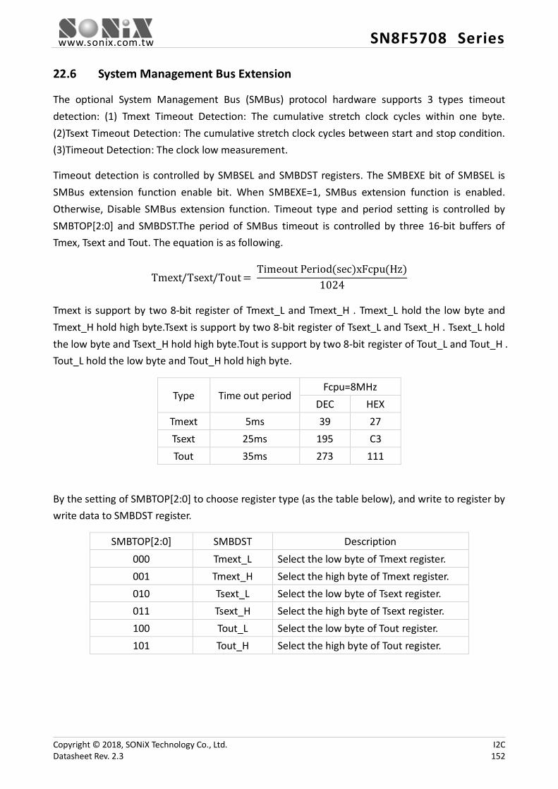
www.sonix.com.tw SN8F5708 Series
22.6 System Management Bus Extension
The optional System Management Bus (SMBus) protocol hardware supports 3 types timeout detection: (1) Tmext Timeout Detection: The cumulative stretch clock cycles within one byte. (2)Tsext Timeout Detection: The cumulative stretch clock cycles between start and stop condition. (3)Timeout Detection: The clock low measurement.
Timeout detection is controlled by SMBSEL and SMBDST registers. The SMBEXE bit of SMBSEL is SMBus extension function enable bit. When SMBEXE=1, SMBus extension function is enabled. Otherwise, Disable SMBus extension function. Timeout type and period setting is controlled by SMBTOP[2:0] and SMBDST.The period of SMBus timeout is controlled by three 16-bit buffers of Tmex, Tsext and Tout. The equation is as following.
Tmext/Tsext/Tout = Timeout Period(sec)xFcpu(Hz)
1024
Tmext is support by two 8-bit register of Tmext_L and Tmext_H . Tmext_L hold the low byte and Tmext_H hold high byte.Tsext is support by two 8-bit register of Tsext_L and Tsext_H . Tsext_L hold the low byte and Tsext_H hold high byte.Tout is support by two 8-bit register of Tout_L and Tout_H . Tout_L hold the low byte and Tout_H hold high byte.
Type Time out period Fcpu=8MHz
DEC HEX Tmext 5ms 39 27 Tsext 25ms 195 C3 Tout 35ms 273 111
By the setting of SMBTOP[2:0] to choose register type (as the table below), and write to register by write data to SMBDST register.
SMBTOP[2:0] SMBDST Description 000 Tmext_L Select the low byte of Tmext register. 001 Tmext_H Select the high byte of Tmext register. 010 Tsext_L Select the low byte of Tsext register. 011 Tsext_H Select the high byte of Tsext register. 100 Tout_L Select the low byte of Tout register. 101 Tout_H Select the high byte of Tout register.
Copyright © 2018, SONiX Technology Co., Ltd. I2C Datasheet Rev. 2.3 152

www.sonix.com.tw SN8F5708 Series
When the SMBus extension function is enabled the lower 3-bit of I2CSTA hold the information about time out as the table below.
I2CSTA Description XXXX X000 No timeout errors. XXXX XXX1 Tout timeout error. XXXX XX1X Tsext timeout error. XXXX X1XX Tmext timeout error.
22.7 I2C Registers
Register Bit 7 Bit 6 Bit 5 Bit 4 Bit 3 Bit 2 Bit 1 Bit 0
I2CDAT I2CDAT7 I2CDAT6 I2CDAT5 I2CDAT4 I2CDAT3 I2CDAT2 I2CDAT1 I2CDAT0 I2CADR ADR6 ADR5 ADR4 ADR3 ADR2 ADR1 ADR0 GC I2CCON CR2 ENS1 STA STO SI AA CR1 CR0 I2CSTA I2CSTA7 I2CSTA6 I2CSTA5 I2CSTA4 I2CSTA3 I2CSTA2 I2CSTA1 I2CSTA0
SMBSEL SMBEXE - - - - SMBSTP2 SMBSTP1 SMBSTP0
SMBDST SMBD7 SMBD6 SMBD5 SMBD4 SMBD3 SMBD2 SMBD1 SMBD0 IEN0 EAL - ET2 ES0 ET1 EX1 ET0 EX0 IEN1 ET2RL - ET2C3 ET2C2 ET2C1 ET2C0 ESPI EI2C P1M P17M P16M P15M P14M P13M P12M P11M P10M P1 P17 P16 P15 P14 P13 P12 P11 P10
I2CDAT Register (0xDA) Bit Field Type Initial Description 7:0 I2CDAT[7:0] R/W 0x00 The I2CDAT register contains a byte to be transmitted
through I2C bus or a byte which has just been received through I2C bus. The CPU can read from and write to this 8-bit, directly addressable SFR while it is not in the process of byte shifting. The I2CDAT register is not shadowed or double buffered so the user should only read I2CDAT when an I2C interrupt occurs.
I2CADR Register (0xDB) Bit Field Type Initial Description 7:1 I2CADR[6:0] R/W 0x00 I2C slave address 0 GC R/W 0 General call address (0X00) acknowledgment
0: ignored 1: recognized
Copyright © 2018, SONiX Technology Co., Ltd. I2C Datasheet Rev. 2.3 153
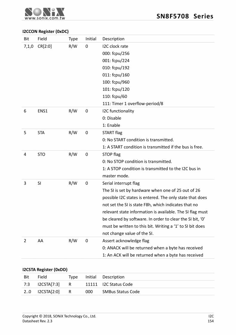
www.sonix.com.tw SN8F5708 Series
I2CCON Register (0xDC) Bit Field Type Initial Description 7,1,0 CR[2:0] R/W 0 I2C clock rate
000: fcpu/256 001: fcpu/224 010: fcpu/192 011: fcpu/160 100: fcpu/960 101: fcpu/120 110: fcpu/60 111: Timer 1 overflow-period/8
6 ENS1 R/W 0 I2C functionality 0: Disable 1: Enable
5 STA R/W 0 START flag 0: No START condition is transmitted. 1: A START condition is transmitted if the bus is free.
4 STO R/W 0 STOP flag 0: No STOP condition is transmitted. 1: A STOP condition is transmitted to the I2C bus in master mode.
3 SI R/W 0 Serial interrupt flag The SI is set by hardware when one of 25 out of 26 possible I2C states is entered. The only state that does not set the SI is state F8h, which indicates that no relevant state information is available. The SI flag must be cleared by software. In order to clear the SI bit, ‘0’ must be written to this bit. Writing a ‘1’ to SI bit does not change value of the SI.
2 AA R/W 0 Assert acknowledge flag 0: ANACK will be returned when a byte has received 1: An ACK will be returned when a byte has received
I2CSTA Register (0xDD) Bit Field Type Initial Description 7:3 I2CSTA[7:3] R 11111 I2C Status Code 2..0 I2CSTA[2:0] R 000 SMBus Status Code
Copyright © 2018, SONiX Technology Co., Ltd. I2C Datasheet Rev. 2.3 154
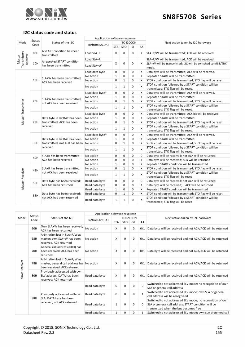
www.sonix.com.tw SN8F5708 Series
I2C status code and status
Mode Status Code
Status of the I2C Application software response
Next action taken by I2C hardware To/from I2CDAT
TO I2CCON STA STO SI AA
Mas
ter
Tran
smitt
er/
Rece
iver
08H A START condition has been transmitted
Load SLA+R X 0 0 X SLA+R/W will be transmitted; ACK will be received
10H A repeated START condition has been transmitted.
Load SLA+R X 0 0 X
SLA+R/W will be transmitted; ACK will be received
Load SLA+W SLA+W will be transmitted; I2C will be switched to MST/TRX mode.
Mas
ter T
rans
mitt
er
18H SLA+W has been transmitted; ACK has been received
Load data byte 0 0 0 X Data byte will be transmitted; ACK will be received. No action 1 0 0 X Repeated START will be transmitted. No action 0 1 0 X STOP condition will be transmitted; STO flag will be reset.
No action 1 1 0 X STOP condition followed by a START condition will be transmitted; STO flag will be reset.
20H SLA+W has been transmitted; not ACK has been received
Load data byte* 0 0 0 X Data byte will be transmitted; ACK will be received. No action 1 0 0 X Repeated START will be transmitted. No action 0 1 0 X STOP condition will be transmitted; STO flag will be reset.
No action 1 1 0 X STOP condition followed by a START condition will be transmitted; STO flag will be reset.
28H Data byte in I2CDAT has been transmitted; ACK has been received
Load data byte 0 0 0 X Data byte will be transmitted; ACK bit will be received. No action 1 0 0 X Repeated START will be transmitted. No action 0 1 0 X STOP condition will be transmitted; STO flag will be reset.
No action 1 1 0 X STOP condition followed by a START condition will be transmitted; STO flag will be reset.
30H Data byte in I2CDAT has been transmitted; not ACK has been received
Load data byte* 0 0 0 X Data byte will be transmitted; ACK will be received. No action 1 0 0 X Repeated START will be transmitted. No action 0 1 0 X STOP condition will be transmitted; STO flag will be reset.
No action 1 1 0 X STOP condition followed by a START condition will be transmitted; STO flag will be reset.
Mas
ter R
ecei
ver
40H SLA+R has been transmitted; ACK has been received
No action 0 0 0 0 Data byte will be received; not ACK will be returned No action 0 0 0 1 Data byte will be received; ACK will be returned
48H SLA+R has been transmitted; not ACK has been received
No action 1 0 0 X Repeated START condition will be transmitted No action 0 1 0 X STOP condition will be transmitted; STO flag will be reset
No action 1 1 0 X STOP condition followed by a START condition will be transmitted; STO flag will be reset
50H Data byte has been received; ACK has been returned
Read data byte 0 0 0 0 Data byte will be received; not ACK will be returned Read data byte 0 0 0 1 Data byte will be received; ACK will be returned
58H Data byte has been received; not ACK has been returned
Read data byte 1 0 0 X Repeated START condition will be transmitted Read data byte 0 1 0 X STOP condition will be transmitted; STO flag will be reset
Read data byte 1 1 0 X STOP condition followed by a START condition will be transmitted; STO flag will be reset
Mode Status Code Status of the I2C
Application software response Next action taken by I2C hardware
To/from I2CDAT TO I2CCON
STA STO SI AA
Slav
e Re
ceiv
er
60H Own SLA+W has been received; ACK has been returned No action X 0 0 0/1 Data byte will be received and not ACK/ACK will be returned
68H Arbitration lost in SLA+R/W as master; own SLA+W has been received, ACK returned
No action X 0 0 0/1 Data byte will be received and not ACK/ACK will be returned
70H General call address (00H) has been received; ACK has been returned
No action X 0 0 0/1 Data byte will be received and not ACK/ACK will be returned
78H Arbitration lost in SLA+R/W as master; general call address has been received, ACK returned
No action X 0 0 0/1 Data byte will be received and not ACK/ACK will be returned
80H Previously addressed with own SLV address; DATA has been received; ACK returned
Read data byte X 0 0 0/1 Data byte will be received and not ACK/ACK will be returned
88H Previously addressed with own SLA; DATA byte has been received; not ACK returned
Read data byte 0 0 0 0 Switched to not addressed SLV mode; no recognition of own SLA or general call address
Read data byte 0 0 0 1 Switched to not addressed SLV mode; own SLA or general call address will be recognized
Read data byte 1 0 0 0 Switched to not addressed SLV mode; no recognition of own SLA or general call address; START condition will be transmitted when the bus becomes free
Read data byte 1 0 0 1 Switched to not addressed SLV mode; own SLA or generalcall
Copyright © 2018, SONiX Technology Co., Ltd. I2C Datasheet Rev. 2.3 155
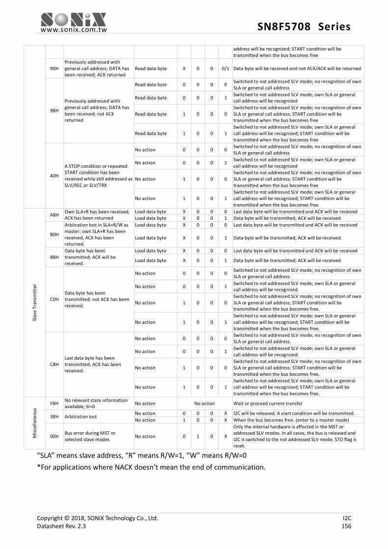
www.sonix.com.tw SN8F5708 Series
address will be recognized; START condition will be transmitted when the bus becomes free
90H Previously addressed with general call address; DATA has been received; ACK returned
Read data byte X 0 0 0/1 Data byte will be received and not ACK/ACK will be returned
98H
Previously addressed with general call address; DATA has been received; not ACK returned
Read data byte 0 0 0 0 Switched to not addressed SLV mode; no recognition of own SLA or general call address
Read data byte 0 0 0 1 Switched to not addressed SLV mode; own SLA or general call address will be recognized
Read data byte 1 0 0 0 Switched to not addressed SLV mode; no recognition of own SLA or general call address; START condition will be transmitted when the bus becomes free
Read data byte 1 0 0 1 Switched to not addressed SLV mode; own SLA or general call address will be recognized; START condition will be transmitted when the bus becomes free
A0H
A STOP condition or repeated START condition has been received while still addressed as SLV/REC or SLV/TRX
No action 0 0 0 0 Switched to not addressed SLV mode; no recognition of own SLA or general call address
No action 0 0 0 1 Switched to not addressed SLV mode; own SLA or general call address will be recognized
No action 1 0 0 0 Switched to not addressed SLV mode; no recognition of own SLA or general call address; START condition will be transmitted when the bus becomes free
No action 1 0 0 1 Switched to not addressed SLV mode; own SLA or general call address will be recognized; START condition will be transmitted when the bus becomes free
Slav
e Tr
ansm
itter
A8H Own SLA+R has been received; ACK has been returned
Load data byte X 0 0 0 Last data byte will be transmitted and ACK will be received Load data byte X 0 0 1 Data byte will be transmitted; ACK will be received.
B0H
Arbitration lost in SLA+R/W as master; own SLA+R has been received, ACK has been returned.
Load data byte X 0 0 0 Last data byte will be transmitted and ACK will be received
Load data byte X 0 0 1 Data byte will be transmitted; ACK will be received.
B8H Data byte has been transmitted; ACK will be received.
Load data byte X 0 0 0 Last data byte will be transmitted and ACK will be received
Load data byte X 0 0 1 Data byte will be transmitted; ACK will be received.
C0H Data byte has been transmitted; not ACK has been received.
No action 0 0 0 0 Switched to not addressed SLV mode; no recognition of own SLA or general call address.
No action 0 0 0 1 Switched to not addressed SLV mode; own SLA or general call address will be recognized.
No action 1 0 0 0 Switched to not addressed SLV mode; no recognition of own SLA or general call address; START condition will be transmitted when the bus becomes free.
No action 1 0 0 1 Switched to not addressed SLV mode; own SLA or general call address will be recognized; START condition will be transmitted when the bus becomes free.
C8H Last data byte has been transmitted; ACK has been received.
No action 0 0 0 0 Switched to not addressed SLV mode; no recognition of own SLA or general call address.
No action 0 0 0 1 Switched to not addressed SLV mode; own SLA or general call address will be recognized.
No action 1 0 0 0 Switched to not addressed SLV mode; no recognition of own SLA or general call address; START condition will be transmitted when the bus becomes free.
No action 1 0 0 1 Switched to not addressed SLV mode; own SLA or general call address will be recognized; START condition will be transmitted when the bus becomes free.
Mis
cella
neou
s
F8H No relevant state information available; SI=0 No action No action Wait or proceed current transfer
38H Arbitration lost No action 0 0 0 X I2C will be released; A start condition will be transmitted. No action 1 0 0 X When the bus becomes free. (enter to a master mode)
00H Bus error during MST or selected slave modes No action 0 1 0 X
Only the internal hardware is affected in the MST or addressed SLV modes. In all cases, the bus is released and I2C is switched to the not addressed SLV mode. STO flag is reset.
“SLA” means slave address, “R” means R/W=1, “W” means R/W=0 *For applications where NACK doesn’t mean the end of communication.
Copyright © 2018, SONiX Technology Co., Ltd. I2C Datasheet Rev. 2.3 156
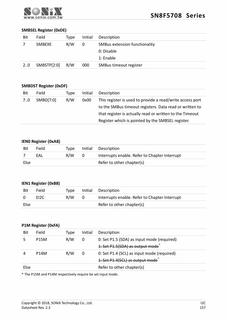
www.sonix.com.tw SN8F5708 Series
SMBSEL Register (0xDE) Bit Field Type Initial Description 7 SMBEXE R/W 0 SMBus extension functionality
0: Disable 1: Enable
2..0 SMBSTP[2:0] R/W 000 SMBus timeout register SMBDST Register (0xDF) Bit Field Type Initial Description 7..0 SMBD[7:0] R/W 0x00 This register is used to provide a read/write access port
to the SMBus timeout registers. Data read or written to that register is actually read or written to the Timeout Register which is pointed by the SMBSEL register.
IEN0 Register (0xA8) Bit Field Type Initial Description 7 EAL R/W 0 Interrupts enable. Refer to Chapter Interrupt Else Refer to other chapter(s)
IEN1 Register (0xB8) Bit Field Type Initial Description 0 EI2C R/W 0 Interrupts enable. Refer to Chapter Interrupt Else Refer to other chapter(s)
P1M Register (0xFA) Bit Field Type Initial Description 5 P15M R/W 0 0: Set P1.5 (SDA) as input mode (required)
1: Set P1.5(SDA) as output mode*
4 P14M R/W 0 0: Set P1.4 (SCL) as input mode (required)
1: Set P1.4(SCL) as output mode* Else Refer to other chapter(s)
* The P15M and P14M respectively require be set input mode.
Copyright © 2018, SONiX Technology Co., Ltd. I2C Datasheet Rev. 2.3 157

www.sonix.com.tw SN8F5708 Series
22.8 Sample Code
The following sample code demonstrates how to perform I2C with interrupt.
1 2 3 4 5 6 7 8 9 10 11 12 13 14 15 16 17 18 19 20 21 22 23 24 25 26 27 28 29 30 31 32 33 34 35 36 37 38 39 40 41 42 43 44 45 46 47 48 49 50 51 52 53
unsigned int I2CAddr; unsigned int I2C_TXData0; unsigned int I2C_TXDatan; unsigned int I2C_RXData0; unsigned int I2C_RXDatan; void I2CInit(void) { P1M &= 0xCF; // P14 & P15 as input
// configure I2Cclock(T1)and enable I2C. I2CCON |= 0xC3; TMOD = 0x60; // auto reload TCON0 = 0x07; // Fosc/1 TH1 = 0xF6; //400kHz TL1 = 0xF6; //400kHz or TH1 = 0xD8; //100kHz TL1 = 0xD8; //100kHz TR1 = 1;
// enable I2C interrupt EI2C = 1; //enable global interrupt EAL = 1;
I2CCON |= 0x20; // START (STA) = 1
} void I2cInterrupt(void) interrupt ISRI2c //0x43 { switch (I2CSTA) { // tx mode case 0x08: I2CCON &= 0xDF; // START (STA) = 0 I2CDAT = I2CAddr; // Tx/Rx addr break; case 0x18: // write first byte I2CDAT = I2C_TXData0; break; case 0x28: // write n byte I2CDAT = I2C_TXDatan; break; case 0x30: // STOP (STO) I2CCON |= 0x10; break; // rx mode case 0x40: // get slave addr I2CCON |= 0x04; // AA = 1 break; case 0x50: // read n byte I2C_RXData0 = I2CDAT; I2CCON &= 0xFB; // AA = 0 break;
Copyright © 2018, SONiX Technology Co., Ltd. I2C Datasheet Rev. 2.3 158

www.sonix.com.tw SN8F5708 Series
54 55 56 57 58 59 60 61 62 63
case 0x58: // read last byte & stop I2C_RXDatan = I2CDAT; I2CCON |= 0x10; // STOP (STO) break; default: I2CCON |= 0x10; // STOP (STO) } I2CCON &= 0xF7; // Clear I2C flag (SI) }
Copyright © 2018, SONiX Technology Co., Ltd. I2C Datasheet Rev. 2.3 159
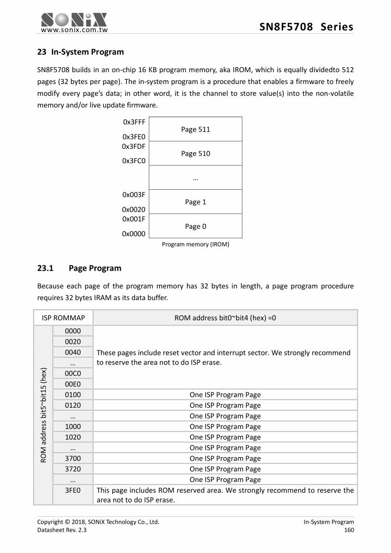
www.sonix.com.tw SN8F5708 Series
23 In-System Program
SN8F5708 builds in an on-chip 16 KB program memory, aka IROM, which is equally dividedto 512 pages (32 bytes per page). The in-system program is a procedure that enables a firmware to freely modify every page’s data; in other word, it is the channel to store value(s) into the non-volatile memory and/or live update firmware.
0x3FFF Page 511
0x3FE0 0x3FDF
Page 510
0x3FC0
…
0x003F
Page 1
0x0020 0x001F
Page 0
0x0000 Program memory (IROM)
23.1 Page Program
Because each page of the program memory has 32 bytes in length, a page program procedure requires 32 bytes IRAM as its data buffer.
ISP ROMMAP ROM address bit0~bit4 (hex) =0
ROM
add
ress
bit5
~bit1
5 (h
ex)
0000
These pages include reset vector and interrupt sector. We strongly recommend to reserve the area not to do ISP erase.
0020 0040
… 00C0 00E0 0100 One ISP Program Page 0120 One ISP Program Page
… One ISP Program Page 1000 One ISP Program Page 1020 One ISP Program Page
… One ISP Program Page 3700 One ISP Program Page 3720 One ISP Program Page
… One ISP Program Page 3FE0 This page includes ROM reserved area. We strongly recommend to reserve the
area not to do ISP erase.
Copyright © 2018, SONiX Technology Co., Ltd. In-System Program Datasheet Rev. 2.3 160

www.sonix.com.tw SN8F5708 Series
These configurations must be setup completely before starting Page Program. ISP is configured using the following steps: 1. Save program data into IRAM. The data continues for 32 bytes. 2. Set the start address of the content location to PERAM. 3. Set the start address of the anticipated update area to PEROM [15:5]. (By PEROMH/PRROML
registers) 4. Write ‘0xA5A’ into PECMD [11:0] to trigger ISP function. Before writing ‘0x5A’ into
PECMD[7:0], PECMD[11:8] must be written ‘0xA’. 5. Write ‘NOP’ instruction twice. As an example, assume the 510th page of program memory (IROM, 0x3FC0 – 0x3FDF) is the anticipated update area; the content is already stored in IRAM address 0x60 – 0x7F. To perform the in-system program, simply write starting IROM address 0x3FC0 to EPROMH/EPROML registers, and then specify buffer starting address 0x60 to EPRAM register. Subsequently, write ‘0xA5A’ into PECMD [11:0] registers to duplicate the buffer’s data to 510th page of IROM.
In general, every page has the capability to be modified by in-system program procedure. However, since the first and least pages (page 0 and 511) respectively stores reset vector and information for power-on controller, incorrectly perform page program (such as turn off power while programming) may cause faulty power-on sequence / reset.
Note:
1. Watch dog timer should be clear before the Flash write (program) operation, or watchdog timer would overflow and reset system during ISP operating.
2. Don’t execute ISP flash ROM program operation for the first page and the last page, or affect program operation.
Copyright © 2018, SONiX Technology Co., Ltd. In-System Program Datasheet Rev. 2.3 161

www.sonix.com.tw SN8F5708 Series
23.2 In-system Program Register
Register Bit 7 Bit 6 Bit 5 Bit 4 Bit 3 Bit 2 Bit 1 Bit 0
PERAM PERAM7 PERAM6 PERAM5 PERAM4 PERAM3 PERAM2 PERAM1 PERAM0
PEROMH PEROM15 PEROM14 PEROM13 PEROM12 PEROM11 PEROM10 PEROM9 PEROM8
PEROML PEROM7 PEROM6 PEROM5 - PECMD11 PECMD10 PECMD9 PECMD8
PECMD PECMD7 PECMD6 PECMD5 PECMD4 PECMD3 PECMD2 PECMD1 PECMD0
PERAM Register (0x97) Bit Field Type Initial Description 7..0 PERAM[7:0] R/W 0x00 The first address of data buffer (IRAM)
PEROMH Register (0x96) Bit Field Type Initial Description 7..0 PEROM[15:8] R/W 0x00 The first address (15th– 8th bit) of program page (IROM)
PEROML Register (0x95) Bit Field Type Initial Description 7..5 PEROM[7:5] R/W 000 The first address (7th– 5th) of program page (IROM) 4 Reserved R 0 3..0 PECMD[11:8] W - 0xA: Enable in-system program
Else values: Disable in-system program*
* Disabling in-system program can avoid mistakenly trigger ISP function.
PECMD Register (0x94) Bit Field Type Initial Description 7..0 PECMD[7:0] W - 0x5A: Start page program procedure*(1)
Else values: Reserved*(2)
*(1) Before writing ‘0x5A’ into PECMD[7:0], PECMD[11:8] must be written ‘0xA’.
*(2) Not permitted to write any other to PECMD register.
Copyright © 2018, SONiX Technology Co., Ltd. In-System Program Datasheet Rev. 2.3 162
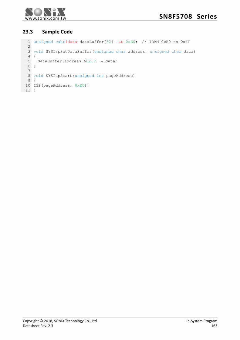
www.sonix.com.tw SN8F5708 Series
23.3 Sample Code
1 2 3 4 5 6 7 8 9 10 11
unsigned cahridata dataBuffer[32] _at_0xE0; // IRAM 0xE0 to 0xFF void SYSIspSetDataBuffer(unsigned char address, unsigned char data) { dataBuffer[address &0x1F] = data; } void SYSIspStart(unsigned int pageAddress) { ISP(pageAddress, 0xE0); }
Copyright © 2018, SONiX Technology Co., Ltd. In-System Program Datasheet Rev. 2.3 163

www.sonix.com.tw SN8F5708 Series
24 Electrical Characteristics
24.1 Absolute Maximum Ratings
Voltage applied at VDD to VSS ...................................................................................... - 0.3V to 6.0V Voltage applied at any pin to VSS ........................................................................ - 0.3V to VDD+0.3V Operating ambient temperature .................................................................................. -40°C to 85°C Storage ambient temperature .....................................................................................-40°C to 125°C Junction Temperature .................................................................................................-40°C to 125°C
24.2 System Operation Characteristics Parameter Test Condition MIN TYP MAX UNIT
VDD Operating voltage fcpu = 1MHz 1.8 5.5 V VDR RAM data retention Voltage 1.5 V VPOR VDD rising rate* 0.05 V/ms
IDD1 Normal mode supply current
VDD = 3V, fcpu = 0.25MHz 2.05 mA VDD = 5V, fcpu = 0.25MHz 2.06 mA VDD = 3V, fcpu = 1MHz 2.25 mA VDD = 5V, fcpu = 1MHz 2.30 mA VDD = 3V, fcpu = 8MHz 3.50 mA VDD = 5V, fcpu = 8MHz 3.55 mA
IDD2 STOP mode supply current VDD = 3V 3.5 8.5 μA VDD = 5V 4.0 9.0 μA
IDD3 IDLE mode supply current (fcpu = 1MHz)
VDD = 3V, 32MHz IHRC 0.63 mA VDD = 5V, 32MHz IHRC 0.65 mA VDD = 3V, 16MHz Crystal 0.65 mA VDD = 5V, 16MHz Crystal 1.25 mA VDD = 3V, 4MHz Crystal 0.60 mA VDD = 5V, 4MHz Crystal 0.75 mA
FIHRC Internal high clock generator
VDD = 1.8V to 5.5V, 25°C 31.84 32 32.16 MHz VDD = 1.8V to 5.5V, 25°C to 85°C
31.68 31.99 MHz
VDD = 1.8V to 5.5V, -40°C to 25°C
32.31 32.64 MHz
FILRC Internal low clock generator VDD = 5V, 25°C 12 16 24 kHz
VLVD18 LVD18 detect voltage 25°C 1.7 1.8 1.9 V -40°C to 85°C 1.6 1.8 2.0 V
VLVD24 LVD24 detect voltage 25°C 2.3 2.4 2.4 V
Copyright © 2018, SONiX Technology Co., Ltd. Electrical Characteristics Datasheet Rev. 2.3 164

www.sonix.com.tw SN8F5708 Series
-40°C to 85°C 2.2 2.4 2.6 V
VLVD33 LVD33 detect voltage 25°C 3.2 3.3 3.4 V -40°C to 85°C 3.0 3.3 3.6 V
* Parameter(s) with star mark are non-verified design reference. Ambient temperature is 25°C.
IHRC Frequency - Temperature Graph
24.3 GPIO Characteristics
Parameter Test Condition MIN TYP MAX UNIT VIL Low-level input voltage VSS 0.3VDD V VIH High-level input voltage 0.7VDD VDD V ILEKG I/O port input leakage current VIN = VDD 2 μA
RUP Pull-up resister VDD = 3V 100 200 300 kΩ VDD = 5V 50 100 150 kΩ
IOH I/O output source current VDD = 5V, VO = VDD-0.5V 12 16 mA
IOL1 I/O sink current (P14 – P17 , P2, P3, P4, P5)
VDD = 5V, VO = VSS+0.5V 15 20 mA
IOL2 I/O sink current (P0, P10 – P13) VDD = 5V, VO = VSS+1.5V 80 100 mA * Ambient temperature is 25°C.
24.4 ADC Characteristics
Parameter Test Condition MIN TYP MAX UNIT VADC Operating voltage 2.0 5.5 V VAIN AIN0 channels input voltage VDD = 5V 0 VREFH V VREFH AVREFH pin input voltage VDD = 5V VREFL+2 VDD V VREFL AVREFL pin input voltage VDD = 5V VSS VREFH-2 V
Copyright © 2018, SONiX Technology Co., Ltd. Electrical Characteristics Datasheet Rev. 2.3 165

www.sonix.com.tw SN8F5708 Series
VEREF External reference voltage VDD = 5V 2.0 VDD V
VIREF
Internal VDD reference voltage VDD = 5V VDD V Internal 4V reference voltage VDD = 5V 3.92 4 4.08 V Internal 3V reference voltage VDD = 5V 2.94 3 3.06 V Internal 2V reference voltage VDD = 5V 1.96 2 2.04 V
IAD ADC current consumption VDD = 3V 0.65 mA VDD = 5V 0.70 mA
f ADCLK ADC clock VDD = 5V 32 MHz f ADSMP ADC sampling rate VDD = 5V 500 kHz t ADEN ADC function enable period VDD = 5V 100 μs
DNL Differential nonlinearity*
f ADSMP = 62.5kHz ±1 LSB f ADSMP = 250kHz ±1 LSB f ADSMP = 500kHz ±4.5 LSB
INL Integral Nonlinearity*
f ADSMP = 62.5kHz ±2 LSB f ADSMP = 250kHz ±2.5 LSB f ADSMP = 500kHz ±4.5 LSB
NMC No missing code*
f ADSMP = 62.5kHz 10 11 12 Bit f ADSMP = 250kHz 11 Bit f ADSMP = 500kHz 9 Bit
VOFFSET Input offset voltage Non-trimmed -10 0 10 mV Trimmed -2 0 2 mV
* Parameters with star mark: VDD = 5V, VREFH = 2.4V, 25°C.
24.5 OPA Characteristics
Parameter Test Condition MIN TYP MAX UNIT VOPA Operating voltage 2.0 5.5 V
IOPA OPA current consumption VDD = 3V 90 μA VDD = 5V 100 μA
VCM Common mode input range VDD = 5V VSS VDD V VOFFSET Input offset voltage VDD = 5V 0 10 mV PSRR Power supply Rejection Ratio* VCM = VSS 50 70 dB CMRR Common mode Rejection Ratio* VCM = -0.3V to 5V, VDD = 5V 50 dB
AOL Open loop gain* VO = 0.2V to VDD-0.2V, VCM = VSS
90 dB
VOS Output voltage swing VOPP = 2.5V VSS+15 VDD-15 mV
ISC Output short current Vdd=5V(Vdd-1/2*Vddand Vss+1/2*Vdd)
25 mA
Copyright © 2018, SONiX Technology Co., Ltd. Electrical Characteristics Datasheet Rev. 2.3 166
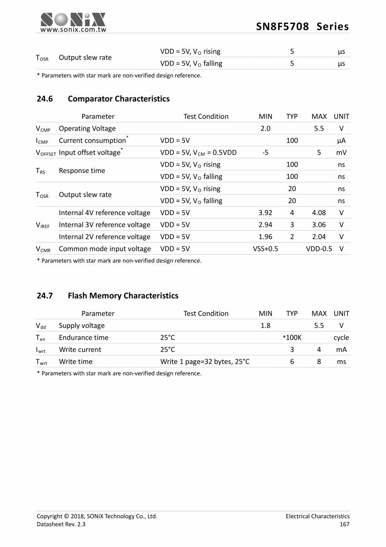
www.sonix.com.tw SN8F5708 Series
TOSR Output slew rate VDD = 5V, VO rising 5 μs VDD = 5V, VO falling 5 μs
* Parameters with star mark are non-verified design reference.
24.6 Comparator Characteristics
Parameter Test Condition MIN TYP MAX UNIT VCMP Operating Voltage 2.0 5.5 V ICMP Current consumption* VDD = 5V 100 μA VOFFSET Input offset voltage* VDD = 5V, VCM = 0.5VDD -5 5 mV
TRS Response time VDD = 5V, VO rising 100 ns VDD = 5V, VO falling 100 ns
TOSR Output slew rate VDD = 5V, VO rising 20 ns VDD = 5V, VO falling 20 ns
VIREF Internal 4V reference voltage VDD = 5V 3.92 4 4.08 V Internal 3V reference voltage VDD = 5V 2.94 3 3.06 V Internal 2V reference voltage VDD = 5V 1.96 2 2.04 V
VCMR Common mode input voltage VDD = 5V VSS+0.5 VDD-0.5 V * Parameters with star mark are non-verified design reference.
24.7 Flash Memory Characteristics
Parameter Test Condition MIN TYP MAX UNIT Vdd Supply voltage 1.8 5.5 V Ten Endurance time 25°C *100K cycle Iwrt Write current 25°C 3 4 mA Twrt Write time Write 1 page=32 bytes, 25°C 6 8 ms * Parameters with star mark are non-verified design reference.
Copyright © 2018, SONiX Technology Co., Ltd. Electrical Characteristics Datasheet Rev. 2.3 167

www.sonix.com.tw SN8F5708 Series
25 Instruction Set
This chapter categorizesthe SN8F5708 microcontroller’s comprehensive assembly instructions. It includes five categories—arithmetic operation, logic operation, data transfer operation, Boolean manipulation, and program branch—which are fully compatible with standard 8051.
Symbol description Symbol Description Rn Working register R0 - R7 direct One of 128 internal RAM locations or any Special Function Register @Ri Indirect internal or external RAM location addressed by register R0 or R1 #data 8-bit constant (immediate operand) #data16 16-bit constant(immediate operand) bit One of 128 software flags located in internal RAM, or any flag of
bit-addressable Special Function Registers addr16 Destination address for LCALL or LJMP, can be anywhere within the 64-Kbyte
page of program memory address space addr11 Destination address for ACALL or AJMP, within the same 2-Kbyte page of
program memory as the first byte of the following instruction rel SJMP and all conditional jumps include an 8-bit offset byte. Its range is
+127/-128 bytes relative to the first byte of the following instruction A Accumulator
Copyright © 2018, SONiX Technology Co., Ltd. Instruction Set Datasheet Rev. 2.3 168
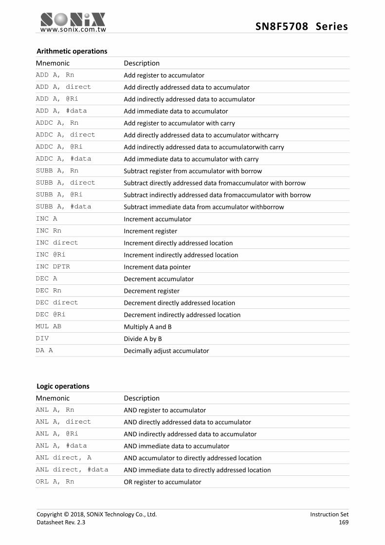
www.sonix.com.tw SN8F5708 Series
Arithmetic operations Mnemonic Description ADD A, Rn Add register to accumulator ADD A, direct Add directly addressed data to accumulator ADD A, @Ri Add indirectly addressed data to accumulator ADD A, #data Add immediate data to accumulator ADDC A, Rn Add register to accumulator with carry ADDC A, direct Add directly addressed data to accumulator withcarry ADDC A, @Ri Add indirectly addressed data to accumulatorwith carry ADDC A, #data Add immediate data to accumulator with carry SUBB A, Rn Subtract register from accumulator with borrow SUBB A, direct Subtract directly addressed data fromaccumulator with borrow SUBB A, @Ri Subtract indirectly addressed data fromaccumulator with borrow SUBB A, #data Subtract immediate data from accumulator withborrow
INC A Increment accumulator INC Rn Increment register INC direct Increment directly addressed location INC @Ri Increment indirectly addressed location INC DPTR Increment data pointer DEC A Decrement accumulator DEC Rn Decrement register DEC direct Decrement directly addressed location DEC @Ri Decrement indirectly addressed location MUL AB Multiply A and B DIV Divide A by B DA A Decimally adjust accumulator
Logic operations Mnemonic Description ANL A, Rn AND register to accumulator ANL A, direct AND directly addressed data to accumulator ANL A, @Ri AND indirectly addressed data to accumulator ANL A, #data AND immediate data to accumulator ANL direct, A AND accumulator to directly addressed location ANL direct, #data AND immediate data to directly addressed location ORL A, Rn OR register to accumulator
Copyright © 2018, SONiX Technology Co., Ltd. Instruction Set Datasheet Rev. 2.3 169
www.sonix.com.tw SN8F5708 Series
ORL A, direct OR directly addressed data to accumulator
ORL A, @Ri OR indirectly addressed data to accumulator ORL A, #data OR immediate data to accumulator ORL direct, A OR accumulator to directly addressed location ORL direct, #data OR immediate data to directly addressed location XRL A, Rn Exclusive OR (XOR) register to accumulator XRL A, direct XOR directly addressed data to accumulator XRL A, @Ri XOR indirectly addressed data to accumulator XRL A, #data XOR immediate data to accumulator XRL direct, A XOR accumulator to directly addressed location XRL direct, #data XOR immediate data to directly addressed location CLR A Clear accumulator CPL A Complement accumulator
RL A Rotate accumulator left RLC A Rotate accumulator left through carry RR A Rotate accumulator right RRC A Rotate accumulator right through carry SWAP A Swap nibbles within the accumulator
Data transfer operations Mnemonic Description MOV A, Rn Move register to accumulator MOV A, direct Move directly addressed data to accumulator MOV A, @Ri Move indirectly addressed data to accumulator MOV A, #data Move immediate data to accumulator MOV Rn, A Move accumulator to register
MOV Rn, direct Move directly addressed data to register MOV Rn, #data Move immediate data to register MOV direct, A Move accumulator to direct MOV direct, Rn Move register to direct MOV direct1, direct2 Move directly addressed data to directly addressed location MOV direct, @Ri Move indirectly addressed data to directly addressed location MOV direct, #data Move immediate data to directly addressed location MOV @Ri, A Move accumulator to indirectly addressed location MOV @Ri, direct Move directly addressed data to indirectly addressed location MOV @Ri, #data Move immediate data to in directly addressed location
Copyright © 2018, SONiX Technology Co., Ltd. Instruction Set Datasheet Rev. 2.3 170
www.sonix.com.tw SN8F5708 Series
MOV DPTR, #data16 Load data pointer with a 16-bit immediate
MOVC A, @A+DPTR Load accumulator with a code byte relative to DPTR MOVC A, @A+PC Load accumulator with a code byte relative to PC MOVX A, @Ri Move external RAM (8-bit address) to accumulator MOVX A, @DPTR Move external RAM (16-bit address) to accumulator MOVX @Ri, A Move accumulator to external RAM (8-bit address) MOVX @DPTR, A Move accumulator to external RAM (16-bit address) PUSH direct Push directly addressed data onto stack POP direct Pop directly addressed location from stack XCH A, Rn Exchange register with accumulator XCH A, direct Exchange directly addressed location with accumulator XCH A, @Ri Exchange indirect RAM with accumulator XCHD A, @Ri Exchange low-order nibbles of indirect and accumulator
Boolean manipulation Mnemonic Description CLR C Clear carry flag CLR bit Clear directly addressed bit SETB C Set carry flag SETB bit Set directly addressed bit CPL C Complement carry flag CPL bit Complement directly addressed bit ANL C, bit AND directly addressed bit to carry flag ANL C, /bit AND complement of directly addressed bit to carry ORL C, bit OR directly addressed bit to carry flag ORL C, /bit OR complement of directly addressed bit to carry
MOV C, bit Move directly addressed bit to carry flag MOV bit, C Move carry flag to directly addressed bit
Copyright © 2018, SONiX Technology Co., Ltd. Instruction Set Datasheet Rev. 2.3 171
www.sonix.com.tw SN8F5708 Series
Program branches Mnemonic Description ACALL addr11 Absolute subroutine call LCALL addr16 Long subroutine call RET Return from subroutine RETI Return from interrupt AJMP addr11 Absolute jump LJMP addr16 Long jump SJMP rel Short jump (relative address) JMP @A+DPTR Jump indirect relative to the DPTR JZ rel Jump if accumulator is zero JNZ rel Jump if accumulator is not zero JC rel Jump if carry flag is set JNC rel Jump if carry flag is not set
JB bit, rel Jump if directly addressed bit is set JNB bit, rel Jump if directly addressed bit is not set JBC bit, rel Jump if directly addressed bit is set and clear bit CJNE A, direct, rel Compare directly addressed data to accumulator and jump if not equal CJNE A, #data, rel Compare immediate data to accumulator and jump if not equal CJNE Rn, #data, rel Compare immediate data to register and jump if not equal CJNE @Ri, #data, rel Compare immediate to indirect and jump if not equal DJNZ Rn, rel Decrement register and jump if not zero DJNZ direct, rel Decrement directly addressed location and jump if not zero NOP No operation for one cycle
Copyright © 2018, SONiX Technology Co., Ltd. Instruction Set Datasheet Rev. 2.3 172
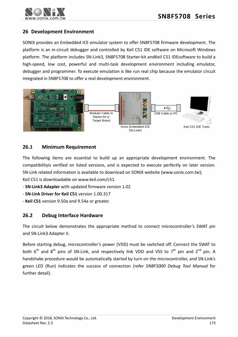
www.sonix.com.tw SN8F5708 Series
26 Development Environment
SONIX provides an Embedded ICE emulator system to offer SN8F5708 firmware development. The platform is an in-circuit debugger and controlled by Keil C51 IDE software on Microsoft Windows platform. The platform includes SN-Link3, SN8F5708 Starter-kit andKeil C51 IDEsoftware to build a high-speed, low cost, powerful and multi-task development environment including emulator, debugger and programmer. To execute emulation is like run real chip because the emulator circuit integrated in SN8F5708 to offer a real development environment.
Keil C51 IDE Tools
USB Cable to PC
Sonix Embedded ICESN-Link3
Modular Cable toStarter-kit orTarget Board
26.1 Minimum Requirement
The following items are essential to build up an appropriate development environment. The compatibilityis verified on listed versions, and is expected to execute perfectly on later version. SN-Link related information is available to download on SONiX website (www.sonix.com.tw); Keil C51 is downloadable on www.keil.com/c51. - SN-Link3 Adapter with updated firmware version 1.02 - SN-Link Driver for Keil C51 version 1.00.317 - Keil C51 version 9.50a and 9.54a or greater.
26.2 Debug Interface Hardware
The circuit below demonstrates the appropriate method to connect microcontroller’s SWAT pin and SN-Link3 Adapter II.
Before starting debug, microcontroller’s power (VDD) must be switched off. Connect the SWAT to both 6th and 8th pins of SN-Link, and respectively link VDD and VSS to 7th pin and 2nd pin. A handshake procedure would be automatically started by turn on the microcontroller, and SN-Link’s green LED (Run) indicates the success of connection (refer SN8F5000 Debug Tool Manual for further detail).
Copyright © 2018, SONiX Technology Co., Ltd. Development Environment Datasheet Rev. 2.3 173

www.sonix.com.tw SN8F5708 Series
3 5 7
2 4 6 8VDD
SWAT SWATVSS
1
example circuit SN-Link header
26.3 Development Tool
SN-Link3 Adapter Starter-Kit support SN8F5708series
MP5 Writer
Copyright © 2018, SONiX Technology Co., Ltd. Development Environment Datasheet Rev. 2.3 174
www.sonix.com.tw SN8F5708 Series
27 SN8F5708 Starter-Kit
SN8F5000 Starter-Kit provides easy-development platform. It includes SN8F5000 family real chip and I/O connectors to input signal or drive device of user’s application.It is a simple platform to develop application as target board not ready. The Starter-Kit can be replaced by target board, because SN8F5000 family integrates embedded ICE in-circuit debugger circuitry.
27.1 Configurations of Circuit
These configurations must be setup completely before starting Starter-Kit developing. 1. Confirm to the circuit board whether elements are complete. 2. The power source of Starter-Kit circuit is chosen from 5.0V, 3.3V, external power or Micro USB
via jumper. 3. The power source comes from 5.0V or 3.3V which must be connect to DC 7.5V power adapter. 4. If the power source is chosen from external power, then external power source connects to
EXT pin. 5. The “RST” pin needs to connect pull high resister to VDD when external reset is chosen to use. 6. The “XIN” pin and the “XOUT” pin need to connect crystal/resonator oscillator components
when system clock is setting crystal or RTC mode. 7. The “XIN” pin needs to connect external clock source when system clock is setting external
clock input mode. 8. The Debug Port can connect SN-LINK Adapter for emulation or download code. 9. The MCU LED will light up and SN8F5000 family chip will be connected to power when power
(VDD) is switched on.
Copyright © 2018, SONiX Technology Co., Ltd. SN8F5708 Starter-Kit Datasheet Rev. 2.3 175

www.sonix.com.tw SN8F5708 Series
27.2 Schematic
27.3 Floor Plan of PCB layout
Copyright © 2018, SONiX Technology Co., Ltd. SN8F5708 Starter-Kit Datasheet Rev. 2.3 176
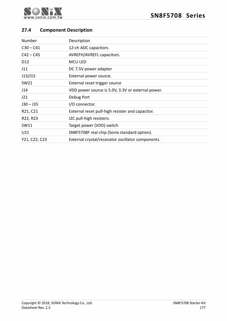
www.sonix.com.tw SN8F5708 Series
27.4 Component Description
Number Description C30 – C41 12-ch ADC capacitors. C42 – C45 AVREFH/AVREFL capacitors. D12 MCU LED J11 DC 7.5V power adapter J13/J15 External power source. SW21 External reset trigger source J14 VDD power source is 5.0V, 3.3V or external power. J21 Debug Port J30 – J35 I/O connector. R21, C21 External reset pull-high resister and capacitor. R22, R23 I2C pull-high resisters. SW11 Target power (VDD) switch U21 SN8F5708F real chip (Sonix standard option). Y21, C22, C23 External crystal/resonator oscillator components.
Copyright © 2018, SONiX Technology Co., Ltd. SN8F5708 Starter-Kit Datasheet Rev. 2.3 177
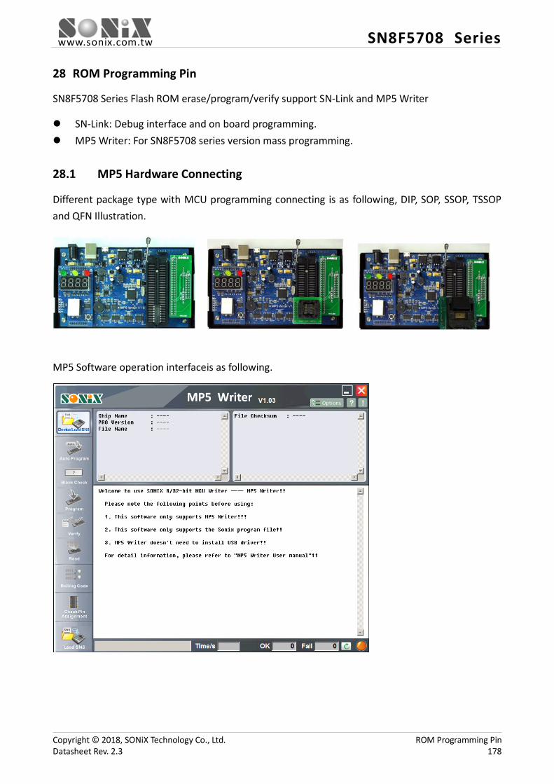
www.sonix.com.tw SN8F5708 Series
28 ROM Programming Pin
SN8F5708 Series Flash ROM erase/program/verify support SN-Link and MP5 Writer
SN-Link: Debug interface and on board programming. MP5 Writer: For SN8F5708 series version mass programming.
28.1 MP5 Hardware Connecting
Different package type with MCU programming connecting is as following, DIP, SOP, SSOP, TSSOP and QFN Illustration.
MP5 Software operation interfaceis as following.
Copyright © 2018, SONiX Technology Co., Ltd. ROM Programming Pin Datasheet Rev. 2.3 178
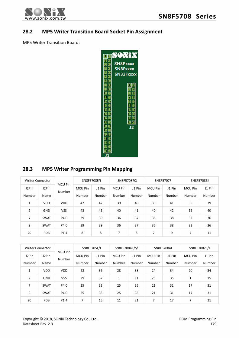
www.sonix.com.tw SN8F5708 Series
28.2 MP5 Writer Transition Board Socket Pin Assignment
MP5 Writer Transition Board:
28.3 MP5 Writer Programming Pin Mapping
Writer Connector MCU Pin
Number
SN8F5708F/J SN8F570870J SN8F5707F SN8F57086J
J2Pin
Number
J2Pin
Name
MCU Pin
Number
J1 Pin
Number
MCU Pin
Number
J1 Pin
Number
MCU Pin
Number
J1 Pin
Number
MCU Pin
Number
J1 Pin
Number
1 VDD VDD 42 42 39 40 39 41 35 39
2 GND VSS 43 43 40 41 40 42 36 40
7 SWAT P4.0 39 39 36 37 36 38 32 36
9 SWAT P4.0 39 39 36 37 36 38 32 36
20 PDB P1.4 8 8 7 8 7 9 7 11
Writer Connector
MCU Pin
Number
SN8F5705F/J SN8F57084K/S/T SN8F57084J SN8F57082S/T
J2Pin
Number
J2Pin
Name
MCU Pin
Number
J1 Pin
Number
MCU Pin
Number
J1 Pin
Number
MCU Pin
Number
J1 Pin
Number
MCU Pin
Number
J1 Pin
Number
1 VDD VDD 28 36 28 38 24 34 20 34
2 GND VSS 29 37 1 11 25 35 1 15
7 SWAT P4.0 25 33 25 35 21 31 17 31
9 SWAT P4.0 25 33 25 35 21 31 17 31
20 PDB P1.4 7 15 11 21 7 17 7 21
Copyright © 2018, SONiX Technology Co., Ltd. ROM Programming Pin Datasheet Rev. 2.3 179
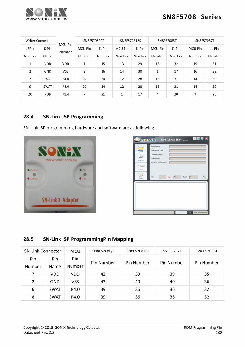
www.sonix.com.tw SN8F5708 Series
Writer Connector
MCU Pin
Number
SN8F570822T SN8F570812S SN8F57085T SN8F57087T
J2Pin
Number
J2Pin
Name
MCU Pin
Number
J1 Pin
Number
MCU Pin
Number
J1 Pin
Number
MCU Pin
Number
J1 Pin
Number
MCU Pin
Number
J1 Pin
Number
1 VDD VDD 1 15 13 29 16 32 15 31
2 GND VSS 2 16 14 30 1 17 16 32
7 SWAT P4.0 20 34 12 28 15 31 14 30
9 SWAT P4.0 20 34 12 28 15 31 14 30
20 PDB P1.4 7 21 1 17 4 20 9 25
28.4 SN-Link ISP Programming
SN-Link ISP programming hardware and software are as following.
28.5 SN-Link ISP ProgrammingPin Mapping
SN-Link Connector MCU Pin
Number
SN8F5708F/J SN8F570870J SN8F5707F SN8F57086J
Pin Number
Pin Name
Pin Number Pin Number Pin Number Pin Number
7 VDD VDD 42 39 39 35 2 GND VSS 43 40 40 36 6 SWAT P4.0 39 36 36 32 8 SWAT P4.0 39 36 36 32
Copyright © 2018, SONiX Technology Co., Ltd. ROM Programming Pin Datasheet Rev. 2.3 180
www.sonix.com.tw SN8F5708 Series
SN-Link Connector MCU Pin
Number
SN8F5705F/J SN8F57084K/S/T SN8F57084J SN8F57082S/T
Pin Number
Pin Name
Pin Number Pin Number Pin Number Pin Number
7 VDD VDD 28 28 24 20 2 GND VSS 29 1 25 1 6 SWAT P4.0 25 25 21 17 8 SWAT P4.0 25 25 21 17
SN-Link Connector MCU
Pin Number
SN8F570822T SN8F570812S SN8F57085T SN8F57087T
Pin Number
Pin Name
Pin Number Pin Number Pin Number Pin Number
7 VDD VDD 1 13 16 15 2 GND VSS 2 14 1 16 6 SWAT P4.0 20 12 15 14 8 SWAT P4.0 20 12 15 14
Copyright © 2018, SONiX Technology Co., Ltd. ROM Programming Pin Datasheet Rev. 2.3 181

www.sonix.com.tw SN8F5708 Series
29 Ordering Information
A typical surface of SONiX microcontroller is printed with three columns: logo, device’s full name, and date code.
SONiX Logo
Full Name S N 8 F 5 7 0 8 J G 8-bit MCU Device Series Package
Date Code 1 5 5 J A E B 1 1 Year Mo. Date Internal Usage
29.1 Device Nomenclature
Full Name Packing Type S8F5708W Wafer SN8F5708H Dice SN8F5708FG LQFP, 48 pins, Green package SN8F5708JG QFN, 48 pins, Green package SN8F570870JG QFN, 46 pins, Green package SN8F5707FG LQFP, 44 pins, Green package SN8F57086JG QFN, 40 pins, Green package SN8F5705FG LQFP, 32 pins, Green package SN8F5705JG QFN, 32 pins, Green package SN8F57084KG SKDIP, 28 pins, Green package SN8F57084SG SOP, 28 pins, Green package SN8F57084TG TSSOP, 28 pins, Green package SN8F57084JG QFN, 28 pins, Green package SN8F57082SG SOP, 20 pins, Green package SN8F57082TG TSSOP, 20 pins, Green package SN8F570822TG TSSOP, 20 pins, Green package SN8F570812SG SOP, 16 pins, Green package SN8F57085TG TSSOP, 16 pins, Green package SN8F57087TG TSSOP, 16 pins, Green package
Copyright © 2018, SONiX Technology Co., Ltd. Ordering Information Datasheet Rev. 2.3 182

www.sonix.com.tw SN8F5708 Series
29.2 Date Code
The date code includes two parts: date of manufacture and production serial code. The first part is public information which is encoded by following principles.
Year 15: 2015 16: 2016 17: 2017 et cetera
Month 1: January 2: February 3: March A: October B: November C: December et cetera
Date 1: 01 2: 02 3: 03 A: 10 B: 11 et cetera
Copyright © 2018, SONiX Technology Co., Ltd. Ordering Information Datasheet Rev. 2.3 183

www.sonix.com.tw SN8F5708 Series
30 Package Information
30.1 LQFP48
Min Typical Max Min Typical Max (inch) (mm)
A 0.063 1.6 A1 0.002 0.006 0.05 0.15 A2 0.053 0.057 1.35 1.45 c1 0.004 0.006 0.09 0.16 D 0.354 BSC 9 BSC
D1 0.276 BSC 7 BSC E 0.354 BSC 9 BSC
E1 0.276 BSC 7 BSC e 0.020 BSC 0.5 BSC B 0.007 0.011 0.17 0.27 L 0.018 0.030 0.45 0.75
L1 0.039 REF 1 REF
Copyright © 2018, SONiX Technology Co., Ltd. Package Information Datasheet Rev. 2.3 184
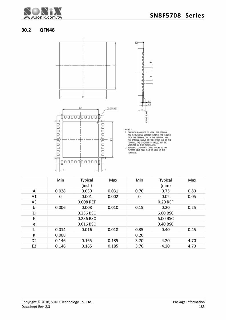
www.sonix.com.tw SN8F5708 Series
30.2 QFN48
Min Typical Max Min Typical Max (inch) (mm)
A 0.028 0.030 0.031 0.70 0.75 0.80 A1 0 0.001 0.002 0 0.02 0.05 A3 0.008 REF 0.20 REF b 0.006 0.008 0.010 0.15 0.20 0.25 D 0.236 BSC 6.00 BSC E 0.236 BSC 6.00 BSC e 0.016 BSC 0.40 BSC L 0.014 0.016 0.018 0.35 0.40 0.45 K 0.008 0.20
D2 0.146 0.165 0.185 3.70 4.20 4.70 E2 0.146 0.165 0.185 3.70 4.20 4.70
Copyright © 2018, SONiX Technology Co., Ltd. Package Information Datasheet Rev. 2.3 185
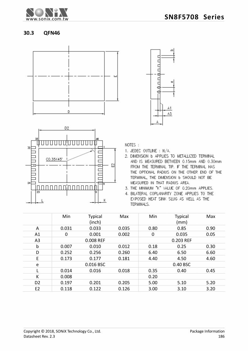
www.sonix.com.tw SN8F5708 Series
30.3 QFN46
Min Typical Max Min Typical Max (inch) (mm)
A 0.031 0.033 0.035 0.80 0.85 0.90 A1 0 0.001 0.002 0 0.035 0.05 A3 0.008 REF 0.203 REF b 0.007 0.010 0.012 0.18 0.25 0.30 D 0.252 0.256 0.260 6.40 6.50 6.60 E 0.173 0.177 0.181 4.40 4.50 4.60 e 0.016 BSC 0.40 BSC L 0.014 0.016 0.018 0.35 0.40 0.45 K 0.008 0.20
D2 0.197 0.201 0.205 5.00 5.10 5.20 E2 0.118 0.122 0.126 3.00 3.10 3.20
Copyright © 2018, SONiX Technology Co., Ltd. Package Information Datasheet Rev. 2.3 186

www.sonix.com.tw SN8F5708 Series
30.4 LQFP44
Min Typical Max Min Typical Max (inch) (mm)
A 0.063 1.6 A1 0.002 0.006 0.05 0.15 A2 0.053 0.055 0.057 1.35 1.40 1.45 c1 0.004 0.006 0.09 0.16 D 0.472 BSC 12 BSC
D1 0.394 BSC 10 BSC E 0.472 BSC 12 BSC
E1 0.394 BSC 10 BSC e 0.031 BSC 0.8 BSC b 0.010 0.012 0.014 0.25 0.30 0.35 L 0.018 0.024 0.030 0.45 0.60 0.75
L1 0.039 REF 1 REF θ° 0° 7° 0° 7°
Copyright © 2018, SONiX Technology Co., Ltd. Package Information Datasheet Rev. 2.3 187

www.sonix.com.tw SN8F5708 Series
30.5 QFN40 5X5
Min Typical Max Min Typical Max (inch) (mm)
A 0.031 0.033 0.035 0.80 0.85 0.90 A1 0 0.001 0.002 0 0.02 0.05 A3 0.008 REF 0.20 REF b 0.006 0.008 0.010 0.15 0.20 0.25 D 0.197 BSC 5.00 BSC E 0.197 BSC 5.00 BSC e 0.016 BSC 0.40 BSC L 0.010 0.012 0.014 0.25 0.30 0.35 K 0.008 0.20
D2 0.147 0.149 0.151 3.74 3.79 3.84 E2 0.147 0.149 0.151 3.74 3.79 3.84
Copyright © 2018, SONiX Technology Co., Ltd. Package Information Datasheet Rev. 2.3 188

www.sonix.com.tw SN8F5708 Series
30.6 LQFP32
Min Typical Max Min Typical Max (inch) (mm)
A 0.063 1.6 A1 0.002 0.004 0.006 0.05 0.10 0.15 A2 0.053 0.055 0.057 1.35 1.40 1.45 c1 0.004 0.005 0.006 0.09 0.125 0.16 D 0.354 BSC 9 BSC
D1 0.276 BSC 7 BSC E 0.354 BSC 9 BSC
E1 0.275 BSC 7 BSC e 0.031 BSC 0.8 BSC b 0.012 0.015 0.018 0.30 0.375 0.45 L 0.018 0.024 0.030 0.45 0.60 0.75
L1 0.039 REF 1 REF
Copyright © 2018, SONiX Technology Co., Ltd. Package Information Datasheet Rev. 2.3 189
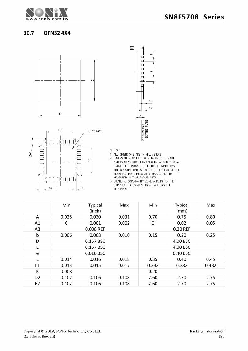
www.sonix.com.tw SN8F5708 Series
30.7 QFN32 4X4
Min Typical Max Min Typical Max (inch) (mm)
A 0.028 0.030 0.031 0.70 0.75 0.80 A1 0 0.001 0.002 0 0.02 0.05 A3 0.008 REF 0.20 REF b 0.006 0.008 0.010 0.15 0.20 0.25 D 0.157 BSC 4.00 BSC E 0.157 BSC 4.00 BSC e 0.016 BSC 0.40 BSC L 0.014 0.016 0.018 0.35 0.40 0.45
L1 0.013 0.015 0.017 0.332 0.382 0.432 K 0.008 0.20
D2 0.102 0.106 0.108 2.60 2.70 2.75 E2 0.102 0.106 0.108 2.60 2.70 2.75
Copyright © 2018, SONiX Technology Co., Ltd. Package Information Datasheet Rev. 2.3 190
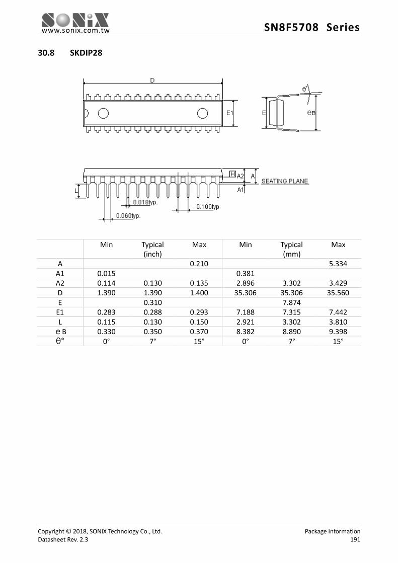
www.sonix.com.tw SN8F5708 Series
30.8 SKDIP28
Min Typical Max Min Typical Max (inch) (mm)
A 0.210 5.334 A1 0.015 0.381 A2 0.114 0.130 0.135 2.896 3.302 3.429 D 1.390 1.390 1.400 35.306 35.306 35.560 E 0.310 7.874
E1 0.283 0.288 0.293 7.188 7.315 7.442 L 0.115 0.130 0.150 2.921 3.302 3.810 eB 0.330 0.350 0.370 8.382 8.890 9.398 θ° 0° 7° 15° 0° 7° 15°
Copyright © 2018, SONiX Technology Co., Ltd. Package Information Datasheet Rev. 2.3 191
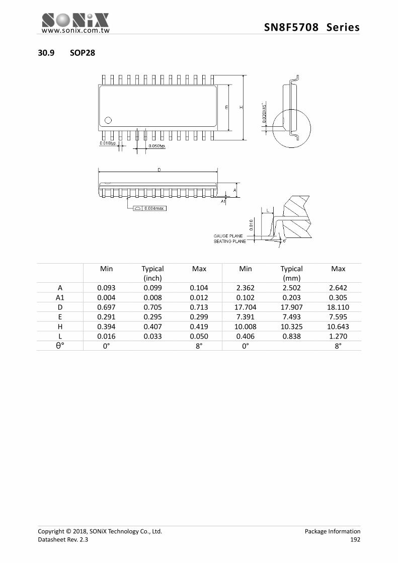
www.sonix.com.tw SN8F5708 Series
30.9 SOP28
Min Typical Max Min Typical Max (inch) (mm)
A 0.093 0.099 0.104 2.362 2.502 2.642 A1 0.004 0.008 0.012 0.102 0.203 0.305 D 0.697 0.705 0.713 17.704 17.907 18.110 E 0.291 0.295 0.299 7.391 7.493 7.595 H 0.394 0.407 0.419 10.008 10.325 10.643 L 0.016 0.033 0.050 0.406 0.838 1.270 θ° 0° 8° 0° 8°
Copyright © 2018, SONiX Technology Co., Ltd. Package Information Datasheet Rev. 2.3 192
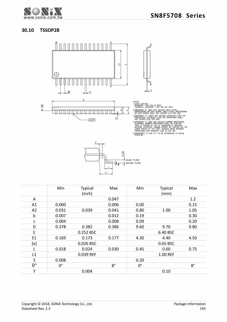
www.sonix.com.tw SN8F5708 Series
30.10 TSSOP28
Min Typical Max Min Typical Max (inch) (mm)
A 0.047 1.2 A1 0.000 0.006 0.00 0.15 A2 0.031 0.039 0.041 0.80 1.00 1.05 b 0.007 0.012 0.19 0.30 c 0.004 0.008 0.09 0.20 D 0.378 0.382 0.386 9.60 9.70 9.80 E 0.252 BSC 6.40 BSC
E1 0.169 0.173 0.177 4.30 4.40 4.50 [e] 0.026 BSC 0.65 BSC L 0.018 0.024 0.030 0.45 0.60 0.75
L1 0.039 REF 1.00 REF S 0.008 0.20 θ° 0° 8° 0° 8° Y 0.004 0.10
Copyright © 2018, SONiX Technology Co., Ltd. Package Information Datasheet Rev. 2.3 193

www.sonix.com.tw SN8F5708 Series
30.11 QFN28 4X4
Min Typical Max Min Typical Max (inch) (mm)
A 0.028 0.030 0.031 0.70 0.75 0.80 A1 0 0.001 0.002 0 0.02 0.05 A3 0.008 REF 0.20 REF b 0.006 0.008 0.010 0.15 0.20 0.25 D 0.157 BSC 4.00 BSC E 0.157 BSC 4.00 BSC e 0.016 BSC 0.40 BSC L 0.014 0.016 0.018 0.35 0.40 0.45 K 0.008 0.20
D2 0.102 0.102 0.104 2.50 2.60 2.65 E2 0.098 0.102 0.104 2.50 2.60 2.65
Copyright © 2018, SONiX Technology Co., Ltd. Package Information Datasheet Rev. 2.3 194

www.sonix.com.tw SN8F5708 Series
30.12 SOP20
Min Typical Max Min Typical Max (inch) (mm)
A 0.093 0.099 0.104 2.362 2.502 2.642 A1 0.004 0.008 0.012 0.102 0.203 0.305 D 0.496 0.502 0.508 12.598 12.751 12.903 E 0.291 0.295 0.299 7.391 7.493 7.595 H 0.394 0.407 0.419 10.008 10.325 10.643 L 0.016 0.033 0.050 0.406 0.838 1.270 θ° 0° 8° 0° 8°
Copyright © 2018, SONiX Technology Co., Ltd. Package Information Datasheet Rev. 2.3 195
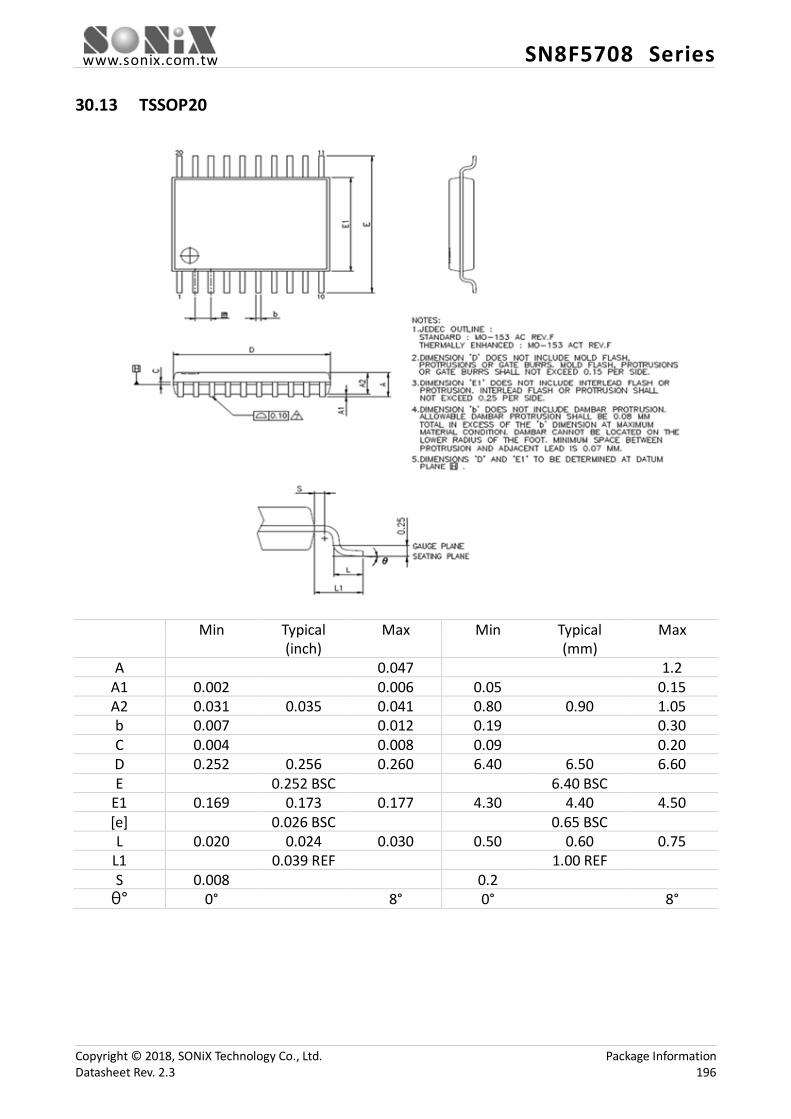
www.sonix.com.tw SN8F5708 Series
30.13 TSSOP20
Min Typical Max Min Typical Max (inch) (mm)
A 0.047 1.2 A1 0.002 0.006 0.05 0.15 A2 0.031 0.035 0.041 0.80 0.90 1.05 b 0.007 0.012 0.19 0.30 C 0.004 0.008 0.09 0.20 D 0.252 0.256 0.260 6.40 6.50 6.60 E 0.252 BSC 6.40 BSC
E1 0.169 0.173 0.177 4.30 4.40 4.50 [e] 0.026 BSC 0.65 BSC L 0.020 0.024 0.030 0.50 0.60 0.75
L1 0.039 REF 1.00 REF S 0.008 0.2 θ° 0° 8° 0° 8°
Copyright © 2018, SONiX Technology Co., Ltd. Package Information Datasheet Rev. 2.3 196

www.sonix.com.tw SN8F5708 Series
30.14 SOP16
Min Typical Max Min Typical Max (inch) (mm)
A 0.069 1.75 A1 0.004 0.010 0.10 0.25 A2 0.049 1.25 - b 0.012 0.020 0.31 0.51 c 0.004 0.010 0.10 0.25 D 0.39BSC 9.90BSC E 0.236BSC 6.00BSC
E1 0.154BSC 3.90BSC e 0.05BSC 1.27BSC h 0.016 0.050 0.40 1.27 L 0.010 0.020 0.25 0.50 θ° 0° 8° 0° 8°
Copyright © 2018, SONiX Technology Co., Ltd. Package Information Datasheet Rev. 2.3 197
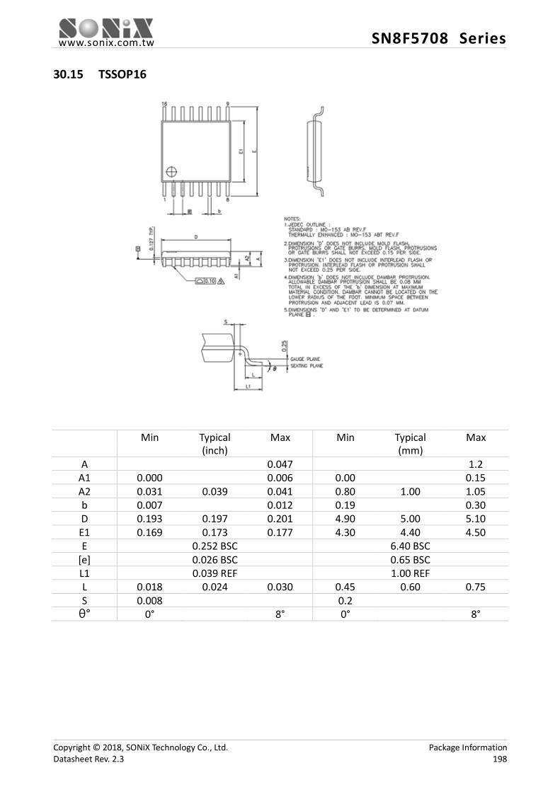
www.sonix.com.tw SN8F5708 Series
30.15 TSSOP16
Min Typical Max Min Typical Max (inch) (mm)
A 0.047 1.2 A1 0.000 0.006 0.00 0.15 A2 0.031 0.039 0.041 0.80 1.00 1.05 b 0.007 0.012 0.19 0.30 D 0.193 0.197 0.201 4.90 5.00 5.10 E1 0.169 0.173 0.177 4.30 4.40 4.50 E 0.252 BSC 6.40 BSC
[e] 0.026 BSC 0.65 BSC L1 0.039 REF 1.00 REF L 0.018 0.024 0.030 0.45 0.60 0.75 S 0.008 0.2 θ° 0° 8° 0° 8°
Copyright © 2018, SONiX Technology Co., Ltd. Package Information Datasheet Rev. 2.3 198
www.sonix.com.tw SN8F5708 Series
31 Appendix: Reference Document
Sonix provides reference document for users to help them quickly familiar SN8F5000 family (downloadable on cooperative website: www.sonix.com.tw).
Document Name Description SN8F5000 Starter-Kit User Manual This documentation introduces SN8F5000
family all Starter-Kit, providing the user selects an appropriate starter-kit for development.
SN8F5000 Family Instruction Set The document details the 8051 instruction set, and a simple example illustrates operation.
SN8F5000 Family Instruction Mapping Table This document supplies the information about mapping assembly instructions from 8-Bit Flash/ OTP Type to 8051 Flash Type.
SN8F5000 Packaging Information This documentation introduces SN8F5000 family microcontrollers’ mechanical data, such as height, width and pitch information.
SN8F5000 Debug Tool Manual This document teaches the user to install software Keil C51, and helped create a new project to be developed.
Copyright © 2018, SONiX Technology Co., Ltd. Appendix: Reference Document Datasheet Rev. 2.3 199

www.sonix.com.tw SN8F5708 Series
SN8F5708 Series Datasheet
8051-based Microcontroller
Corporate Headquarters 10F-1, No.36, Taiyuan St. Chupei City, Hsinchu, Taiwan TEL: +886-3-5600888 FAX: +886-3-5600889 Taipei Sales Office 15F-2, No.171,Songde Rd. Taipei City, Taiwan TEL: +886-2-27591980 FAX: +886-2-27598180 [email protected] [email protected]
Hong Kong Sales Office Unit 2603, No. 11, Wo Shing St. Fo Tan, Hong Kong TEL: +852-2723-8086 FAX: +852-2723-9179 [email protected] Shenzhen Contact Office High Tech Industrial Park, Shenzhen, China TEL: +86-755-2671-9666 FAX: +86-755-2671-9786 [email protected] [email protected]
USA Office TEL: +1-714-3309877 TEL: +1-949-4686539 [email protected] Japan Office 2F, 4 Chome-8-27Kudanminami Chiyoda-ku,Tokyo, Japan TEL: +81-3-6272-6070 FAX: +81-3-6272-6165 [email protected] FAE Support via email 8-bit Microcontroller Products: [email protected] All Products: [email protected]
Copyright © 2018, SONiX Technology Co., Ltd. Appendix: Reference Document Datasheet Rev. 2.3 200