Embed Size (px)
Citation preview
SmartSpice Analog Circuit Simulator
Device Models
SmartSpice Analog Circuit Simulator
SmartSpice Background
Development started in 1986 with 3A1; incorporated major changes and standardized software development on coding rules of 3C.1 and 3D.2 releases
Objective - complete solution to Analog Circuit Simulation requirements
True C/C++ language architecture to take advantage over the other vendors still based on FORTRAN language
Final product has the advantage of being compatible with standard Berkeley SPICE syntax and data structures
- 2 -

SmartSpice Analog Circuit Simulator
SmartSpice Background (con’t)
Rapid acceptance as the industry standard worldwide Large customer base All major companies have a copy of SmartSpice Broad spectrum of users from individuals and Startups to large
multinationals.
- 3 -
SmartSpice Analog Circuit Simulator
Device Models
Supports a comprehensive set of public domain device models All models support advanced convergence algorithms,
temperature dependencies, gate capacitance models and geometry calculation methods
- 4 -
SmartSpice Analog Circuit Simulator
Device Models (con’t)
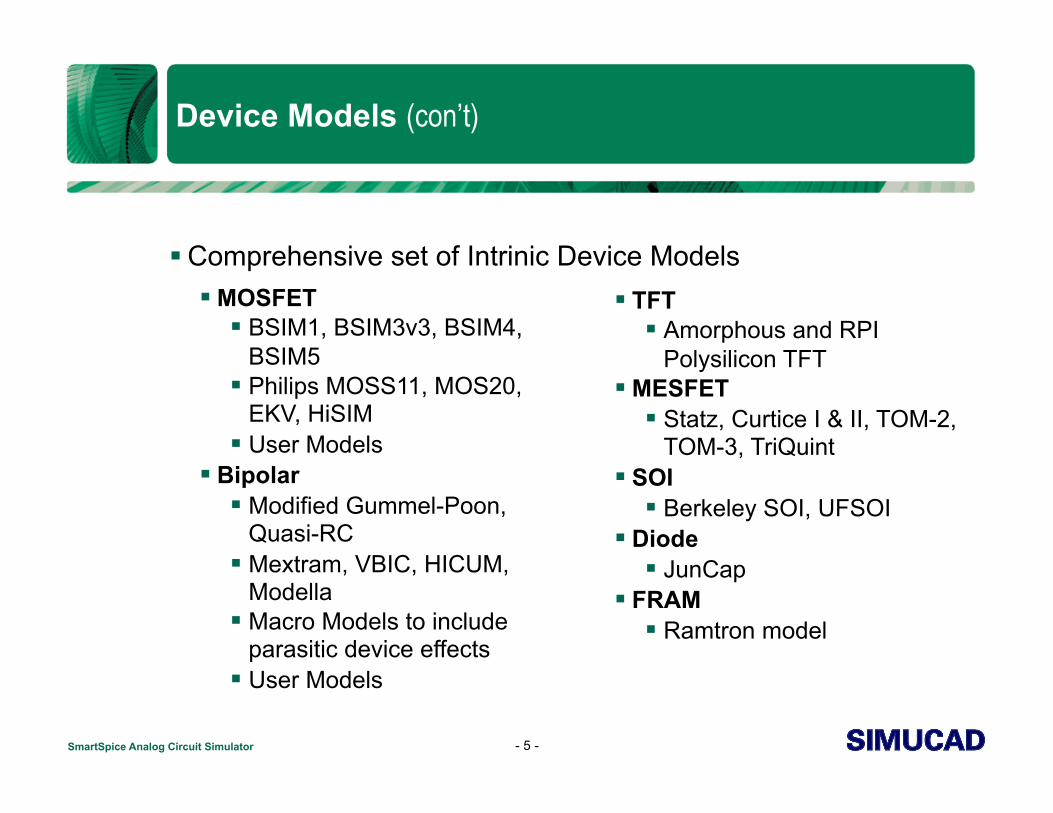
MOSFET BSIM1, BSIM3v3, BSIM4,
BSIM5 Philips MOSS11, MOS20,
EKV, HiSIM User Models
Bipolar Modified Gummel-Poon,
Quasi-RC Mextram, VBIC, HICUM,
Modella Macro Models to include
parasitic device effects User Models
TFT Amorphous and RPI
Polysilicon TFT MESFET
Statz, Curtice I & II, TOM-2, TOM-3, TriQuint
SOI Berkeley SOI, UFSOI
Diode JunCap
FRAM Ramtron model
- 5 -
Comprehensive set of Intrinic Device Models

SmartSpice Analog Circuit Simulator
Device Models: BJTs
LEVEL 1: Modified Gummel-Poon model LEVEL 2: Quasi RC (quasi-saturation) model
- 6 -

SmartSpice Analog Circuit Simulator
Bipolar Models
MEXTRAM (Level=503): Improved modeling of substrate effects and parasitic pnp Improved approximation of distributed high frequency
effects in the intrinsic base VBIC (Level=5):
Temperature dependency for knee currents and intrinsic/extrinsic resistances
BVBE model High current roll-off
HICUM (Level=6): High Current model for high speed applications High collector currents (quasi-sat and saturation) Large-signal transient applications Good fit for SiGe HBTs
- 7 -
SmartSpice Analog Circuit Simulator
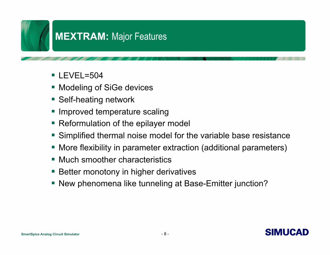
MEXTRAM: Major Features
LEVEL=504 Modeling of SiGe devices Self-heating network Improved temperature scaling Reformulation of the epilayer model Simplified thermal noise model for the variable base resistance More flexibility in parameter extraction (additional parameters) Much smoother characteristics Better monotony in higher derivatives New phenomena like tunneling at Base-Emitter junction?
- 8 -

SmartSpice Analog Circuit Simulator
VBIC: Major Features
Improved Early effect modeling Parasitic PNP (substrate current effect) Quasi-saturation modeling with modified Kull model Constant overlap capacitances Weak avalanche model Improved depletion and diffusion capacitance First order modeling of distributed base Improved temperature modeling Excess phase network Self-heating HBT modeling ability
- 9 -

SmartSpice Analog Circuit Simulator
VBIC: Major Features (con’t)
Reach-through model to limit base-collector depletion capacitance Simple Base-Emitter breakdown model Fixed collector-substrate oxide capacitance Selector to switch to SGP qb formulation High current roll-off coefficient Separate IS allowed for reverse operation in HBTs Additional parameters added to extend temperature mappings
temperature dependence of IKF separate coefficients for intrinsic and extrinsic resistances separate activation energy for ISP
- 10 -

SmartSpice Analog Circuit Simulator
VBIC: Additional Effects
Weak avalanche model based on Kloosterman and De Graaff model (MEXTRAM)
Base resistance split into intrinsic and extrinsic part Rbi modulated by qb to include depletion pinching and high injection
effects Parasitic PNP device
based on a partial GP model (no Early effect included) most important parts are Iccp and Qbcp Rbip modulated by qbp (similarly to Rbi)
Distributed base (first order approximation) partitioning of Ibe and qje across Rbi applies to both AC and DC modeling
- 11 -

SmartSpice Analog Circuit Simulator
HICUM: Major Features
Accurate description of the high-current operating region Distributed modeling of external base-collector region Emitter periphery injection and charge storage accounted for Bias dependent internal base resistance Prediction of temperature and process variations (scalability) Parasitic capacitances representing B-E and B-C oxide overlaps B-C weak avalanche breakdown and B-E tunneling Collector current spreading included in Ic and Qf expressions Simple parasitic substrate transistor and RC network Self-heating and Non-Quasi-Static effects
- 12 -

SmartSpice Analog Circuit Simulator
Device Models: BJTs
LEVEL 500: Philips MODELLA model Temperature effect Charge storage effects Excess phase shift for current and storage charges Substrate effects High-injection effects Build-in electric field in base region Bias-dependent early effect low-level non-ideal base currents Hard and quasi-saturation Weak avalanche Hot carrier effects in the collector epilayer Explicit modeling of inactive region
- 13 -

SmartSpice Analog Circuit Simulator
Hetrojunction Bipolar Transistor (HBT) Models
LEVEL 20: UCSD-HBT model Based on the standard SPICE Gummel-Poon model
- 14 -

SmartSpice Analog Circuit Simulator
Device Models: MOSFETs
LEVEL 1: Schichman-Hodges model LEVEL 2: Modified Schichman-Hodges model LEVEL 3: Semi-empirical model LEVEL 4: BSIM1 LEVEL 7: BSIM3
- 15 -
SmartSpice Analog Circuit Simulator
Device Models: MOSFETs
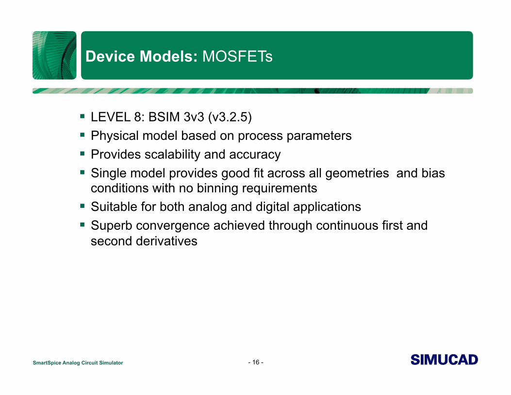
LEVEL 8: BSIM 3v3 (v3.2.5) Physical model based on process parameters Provides scalability and accuracy Single model provides good fit across all geometries and bias
conditions with no binning requirements Suitable for both analog and digital applications Superb convergence achieved through continuous first and
second derivatives
- 16 -

SmartSpice Analog Circuit Simulator
BSIM3 Model
Developed by UC Berkeley Most recent release is BSIM3 Version 3 Physical and scaleable properties Built-in W, L, Nch(x), TOX, XJ, RDS, LDD and T dependencies
for drain current and first derivatives Support for current and future developments in MOSFET
technologies Simulation of devices with channel length down to 0.13µ and oxide
thickness down to 50A Can be used for statistical modeling
- 17 -

SmartSpice Analog Circuit Simulator
BSIM3 Model (cont.)
Threshold voltage reduction Mobility degradation due to gate vertical field Non-uniform doping effects Carrier velocity saturation and channel length modulation Drain induced barrier lowering (DIBL) Substrate current induced body effect Subthreshold current model Single I-V expression describes all operating regions Capacitance model for short and narrow geometry devices
- 18 -

SmartSpice Analog Circuit Simulator
BSIM3 Model (cont.)
Simucad enhancements to the standard BSIM3 models include: Advanced geometry and scaling models based on the Area Calculation
Method Temperature models consistent with other MOSFET models for both
the model kernel and models parasitics Multiplier for parallel connected devices Devices outputs, such as terminal currents and device capacitances
- 19 -
SmartSpice Analog Circuit Simulator
BSIM3 Version 3 Implementation
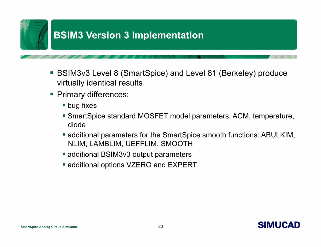
BSIM3v3 Level 8 (SmartSpice) and Level 81 (Berkeley) produce virtually identical results
Primary differences: bug fixes SmartSpice standard MOSFET model parameters: ACM, temperature,
diode additional parameters for the SmartSpice smooth functions: ABULKIM,
NLIM, LAMBLIM, UEFFLIM, SMOOTH additional BSIM3v3 output parameters additional options VZERO and EXPERT
- 20 -

SmartSpice Analog Circuit Simulator
BSIM3 Version 3 Convergence
Berkeley smooth functions: Vbseff, Vgsteff, Vdseff, Vgs_overlap, Vfb_eff
SmartSpice smooth functions for Abulk >= 0.01, n >=1, lambda=A1*Vgsteff+A2 <=1, Ngate, ueff
CONV option (GMIN and DCGMIN stepping algorithms) EXPERT option for discontinuity detection Convergence properties of BSIM3 Version 3 are better than
convergence properties of BSIM3 Version 2
- 21 -

SmartSpice Analog Circuit Simulator
Parameter Check in BSIM3 Model (con’t)
In the original Berkeley BSIM 3.1 implementation, there are two types of checks - default (unconditional) check, and a check invoked by the parameter PARAMCHK=1:
- 22 -
Corrected Errors: Corrected Errors:
if( CJSW>0.0 || CJSWG>0.0 ){ if(A2 < 0.01) { A2 = 0.01 if (PD < Weff) if(A2 > 1.0) PD = Weff A2 = 1.0 if (PS < Weff) A1 = 0.0 PS = Weff if(RDSW < 0.0) } RDSW = 0.0 Rds0 = 0.0 if(Rds0> 0.0 && Rds0 < 0.001) Rds0 = 0.0 if(CGDO < 0.0) CGDO = 0.0 if(CGSO < 0.0) CGSO = 0.0 if(CGBO < 0.0) CGBO = 0.0
Default PARAMCHK=1 Check Check
Fatal errors: Warnings:
Leff <= 0.0 Leff <= 5.0e-8 Weff <= 0.0 LeffCV <= 5.0e-8 LeffCV <= 0.0 Weff <= 1.0e-7 WeffCV <= 0.0 WeffCV <= 1.0e-7 TOX <= 0.0 TOX < 1.0e-9 NLX < -Leff NLX < 0.0 NPEAK <= 0.0 NPEAK <= 1.0e15 NSUB <= 0.0 NPEAK >= 1.0e21 NGATE < 0.0 NSUB <= 1.0e14 NGATE > 1.e25 NSUB >= 1.0e21 XJ <= 0.0 NGATE > 0.0 && <= 1.e18 DVT1 < 0.0 DVT0 < 0.0 DVT1W < 0.0 CDSC < 0.0 W0 = -Weff CDSCD < 0.0 DSUB < 0.0 ETA0 < 0.0 B1 = -Weff fabs(1e-6/(B1+Weff)) > 10 CLC < 0.0 fabs(1e-6/(W0+Weff)) > 10 DELTA < 0.0 PDIBLC1 < 0.0 PCLM <= 0.0 PDIBLC2 < 0.0 DROUT < 0.0 Vsattemp <= 0.0 Vsattemp < 1.0e3

SmartSpice Analog Circuit Simulator
BSIM4 MOSFET Model
Level=14 : original SmartSpice implementation Level=54 : compatibility with HSPICE(TM) implementation Improvements and additions over BSIM3v3 Accurate new model of the intrinsic input resistance Flexible substrate resistance network New accurate channel thermal noise and flicker noise NQS model consistent with Rg-based RF model
Accurate gate direct tunnelling model Comprehensive geometry-dependent parasitics model Asymmetrical and bias-dependent S/D model More accurate mobility model GIDL current model Quantum mechanical charge-layer-thickness model Different diode IV and CV characteristics
- 23 -
SmartSpice Analog Circuit Simulator
Device Models: MOSFETs
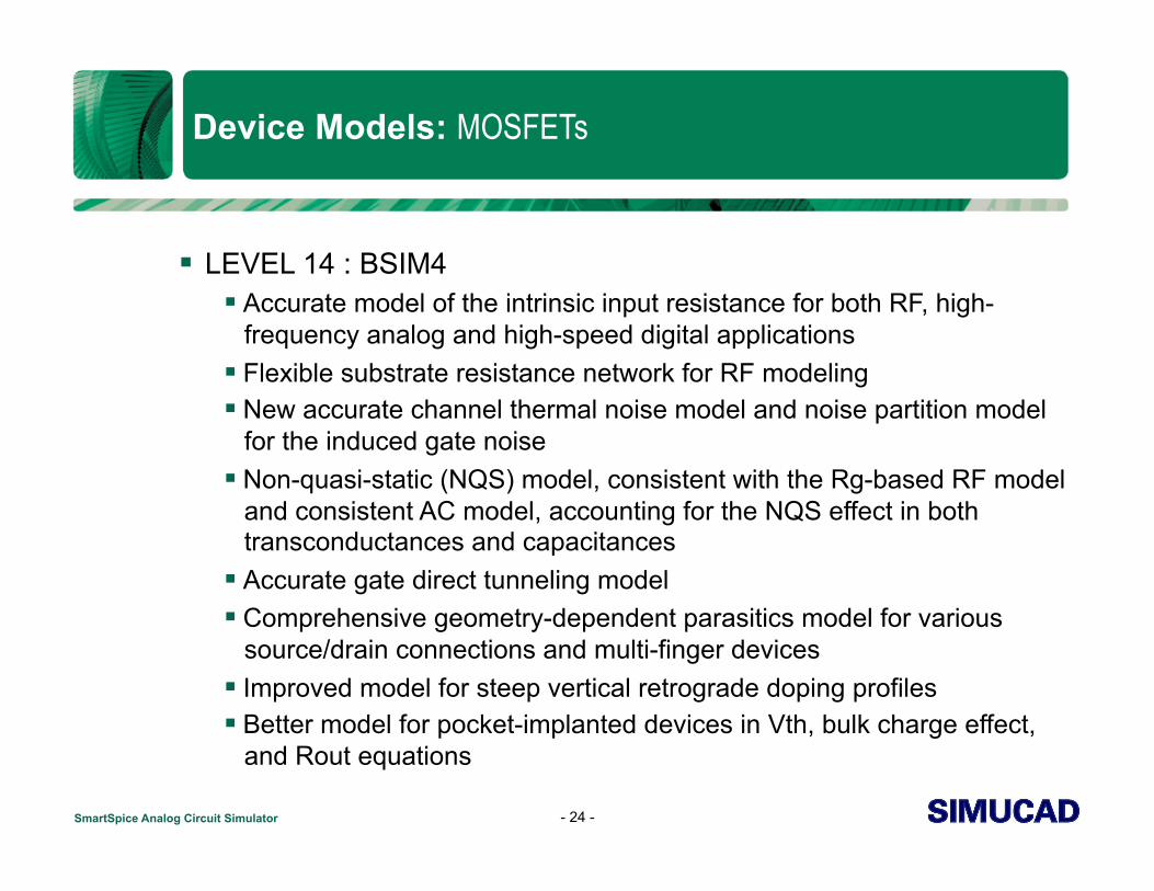
LEVEL 14 : BSIM4 Accurate model of the intrinsic input resistance for both RF, high-
frequency analog and high-speed digital applications Flexible substrate resistance network for RF modeling New accurate channel thermal noise model and noise partition model
for the induced gate noise Non-quasi-static (NQS) model, consistent with the Rg-based RF model
and consistent AC model, accounting for the NQS effect in both transconductances and capacitances
Accurate gate direct tunneling model Comprehensive geometry-dependent parasitics model for various
source/drain connections and multi-finger devices Improved model for steep vertical retrograde doping profiles Better model for pocket-implanted devices in Vth, bulk charge effect,
and Rout equations
- 24 -
SmartSpice Analog Circuit Simulator
Device Models: MOSFETs (con’t)
LEVEL 14 : BSIM4 (continued) Asymmetrical and bias-dependent source/drain resistance, either
internal or external to the intrinsic MOSFET Acceptance of either the electrical or physical gate Oxide thickness as the model input at the user’s choice in a physically
accurate manner Quantum mechanical charge-layer-thickness model for both IV and CV More accurate mobility model for predictive modeling Gate-induced drain leakage (GIDL) current model, available in BSIM
for the first time Improved unified flicker (1/f) noise model, smooth over all bias regions
and accounting for the bulk charge effect Different diode IV and CV characteristics for source and drain
junctions Junction diode breakdown with or without current limiting Gate dielectric constant defined as a model parameter
- 25 -

SmartSpice Analog Circuit Simulator
Device Models: MOSFETs (con’t)
LEVEL 55 : BSIM5 Built on the well-proven BSIM4 Improvements with regard to previous BSIM3v3 and BSIM4 :
Fully physical and symmetric Improved reciprocity (no negative capacitances) Better model for moderate inversion region
Better core using as much as possible of BSIM4 features
- 26 -

SmartSpice Analog Circuit Simulator
Device Models: MOSFETs (con’t)
LEVEL 11: Philips MOS11 model Dedicated to analog, RF and digital simulation Physics based Based on surface potentials
Accurate transition from weak to strong inversion Single equation for the whole operating range
Symmetrical Good distortion behavior (accurate description of high-order
derivatives)
- 27 -

SmartSpice Analog Circuit Simulator
Device Models: MOSFETs (con’t)
LEVEL 20: Philips MOS20 model High-Voltage MOSFET model Especially developed to describe LDMOS, EPMOS and VDMOS
models Acts as a replacement for the couple MOS9+MOS30 Includes the following effects:
Surface potentials computation avoiding smoothing functions between operating regimes
Mobility reduction Velocity saturation Drain-Induced Barrier Lowering (DIBL) Static feedback Channel length modulation Weak avalanche current
- 28 -

SmartSpice Analog Circuit Simulator
Device Models: MOSFETs (con’t)
LEVEL 44: EKV MOSFET model Simulation of low voltage, low current analog and mixed signal circuits
using submicron CMOS technologies EKV model equation is based on single expression, preserves
continuity of first and higher order derivatives Includes the following physical effects:
Effects of doping profile, substrate effect Modeling of weak, moderate and strong inversion behavior Modeling of mobility effect due to vertical field Short channel effects for velocity saturation, channel length modulation
(CLM), source and drain charge-sharing (including for narrow channel widths), reverse short-channel effect (RSCE)
Modeling of substrate current due to impact ionization Quasi-static charge-based dynamic model Thermal and flicker noise modeling
- 29 -
SmartSpice Analog Circuit Simulator
Device Models: MOSFETs (con’t)
LEVEL 88: High voltage MOSFET model Forward and reverse mode of operations Asymmetry of all parasitics (diodes and resistances) Bias dependence of external resistances RDS Dependence mobility degradation on Vds Bias dependent VSAT Transconductance Gm reduction in saturation at high Vds
- 30 -

SmartSpice Analog Circuit Simulator
HiSIM MOSFET Model
HiSIM version 1.2.0 Computes surface potentials, from the drift-diffusion approximation
No parameter inter-dependence Easy parameter extraction Low number of parameters Continuity of derivatives One parameter set for all channel lengths
- 31 -
SmartSpice Analog Circuit Simulator
Device Models: MOSFETs
LEVEL 111: HiSIM MOSFET model Computes surface potentials, from the drift-diffusion approximation
No parameter inter-dependence Easy parameter extraction Low number of parameters Continuity of derivatives One parameter set for all channel lengths
- 32 -
SmartSpice Analog Circuit Simulator
Thin Film Transistors (TFT) Models
Amorphous-Silicon TFT models: LEVEL 15: Modified Leroux model
Transport by multitraps Channel length modulation (CLM) Exponential localized states density Temperature dependence Overlap resistance Rc
- 33 -

SmartSpice Analog Circuit Simulator
TFT Models - Leroux’s Model a-Si (Level 15)
Leakage current : empirical equation Exponential dependence of subthreshold current with vgs CLM effect taken into account in saturation region Temperature dependence Charge-conservation model (fast convergence in transient) Transitions with model parameters : VGHIGH, VGLOW Simple but well proven model
- 34 -
SmartSpice Analog Circuit Simulator
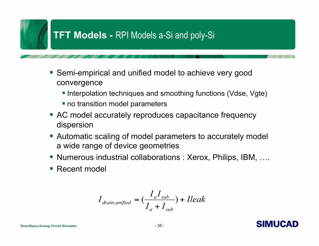
TFT Models - RPI Models a-Si and poly-Si
Semi-empirical and unified model to achieve very good convergence Interpolation techniques and smoothing functions (Vdse, Vgte) no transition model parameters
AC model accurately reproduces capacitance frequency dispersion
Automatic scaling of model parameters to accurately model a wide range of device geometries
Numerous industrial collaborations : Xerox, Philips, IBM, …. Recent model
- 35 -
IleakIIIIIsuba
subaunifieddrain +
+= )(,

SmartSpice Analog Circuit Simulator
RPI Polysilicon and Amorphous TFT Models
Self heating is added to both models via single internal thermal mode. Thermal circuit is represented with a thermal resistance and capacitance in parallel
New charge conservation model based on Leroux’s model founded on a single parameter
- 36 -

SmartSpice Analog Circuit Simulator
Thin Film Transistors (TFT) Models
LEVEL 35: Modified RPI model Unified DC model covers all regimes of operation AC model accurately reproduces frequency dispersion
of capacitances Provides automatic scaling of model parameters to accurately model a
wide range of device geometries
- 37 -

SmartSpice Analog Circuit Simulator
Thin Film Transistors (TFT) Models (con’t)
Polysilicon TFT models: LEVEL 16: Modified U.C. Berkeley SPICE 3E1 model
Hot carrier Drain induced barrier lowering (DIBL) Channel length modulation (CLM) Thermal generation Gate induced drain leakage (GIDL)
- 38 -
SmartSpice Analog Circuit Simulator
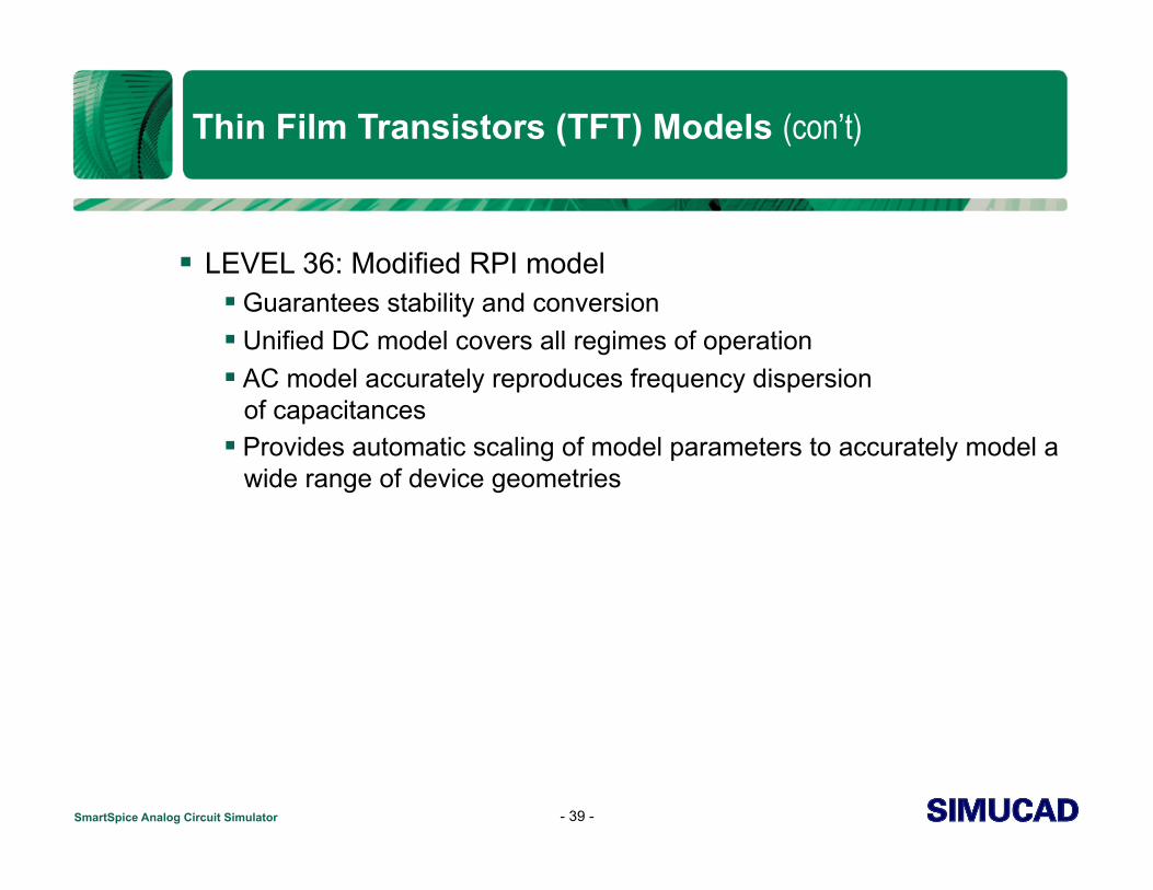
Thin Film Transistors (TFT) Models (con’t)
LEVEL 36: Modified RPI model Guarantees stability and conversion Unified DC model covers all regimes of operation AC model accurately reproduces frequency dispersion
of capacitances Provides automatic scaling of model parameters to accurately model a
wide range of device geometries
- 39 -

SmartSpice Analog Circuit Simulator
SOI Model Features
Continuity of DC current and its derivatives in all regions of operation
Charge and physical based model Charge-conservation models Suitable for deep-submicron devices Scalable and accurate model DC, AC, transient and noise analysis Floating body voltage iterated by SPICE engine
(determined by body currents)
- 40 -

SmartSpice Analog Circuit Simulator
Advanced SPICE Model Implementation in SmartSpice: SOI Model Objectives
Dynamic depletion is applied on both I-V and C-V. Charge and Drain current are scaleable with Tbox and Tsi continuously
Supports external body bias and backgate bias; a total of 6 nodes Real floating body simulation in both I-V and C-V Body potential is
properly bounded by diode and C-V formulation Self heating implementation improved over the alpha version
- 41 -

SmartSpice Analog Circuit Simulator
Advanced SPICE Model Implementation in SmartSpice: SOI Model Objectives (con’t)
An improved impact ionization current model Various diode leakage components and parasitic bipolar current
included New depletion charge model (EBCI) introduced for better accuracy
in capacitive coupling prediction. An improved BSIM3v3 based model is added as well
Dynamic depletion selector (ddMod) to suit different requirements for SOI technologies
Single I-V expression as in BSIM3v3.1 to guarantee continuities of Ids, Gds and Gm and their derivatives for all bias conditions
- 42 -

SmartSpice Analog Circuit Simulator
SOI Models
LEVEL 21 : UFS (Florida) SOI model fully depleted: Physically accounts for the charge coupling between the front and
the back gates 2-D analysis for the subthreshold region of operation has been added Accumulation of charge in the body has been also added, it can drive
dynamic floating-body bipolar effects Accounts for DC and dynamic floating-body effects in all regions of
operation
- 43 -
SmartSpice Analog Circuit Simulator
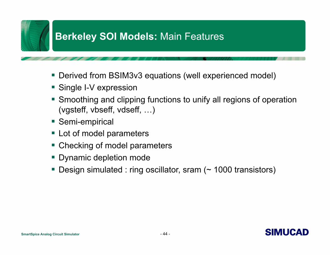
Berkeley SOI Models: Main Features
Derived from BSIM3v3 equations (well experienced model) Single I-V expression Smoothing and clipping functions to unify all regions of operation
(vgsteff, vbseff, vdseff, …) Semi-empirical Lot of model parameters Checking of model parameters Dynamic depletion mode Design simulated : ring oscillator, sram (~ 1000 transistors)
- 44 -
SmartSpice Analog Circuit Simulator
SOI Models
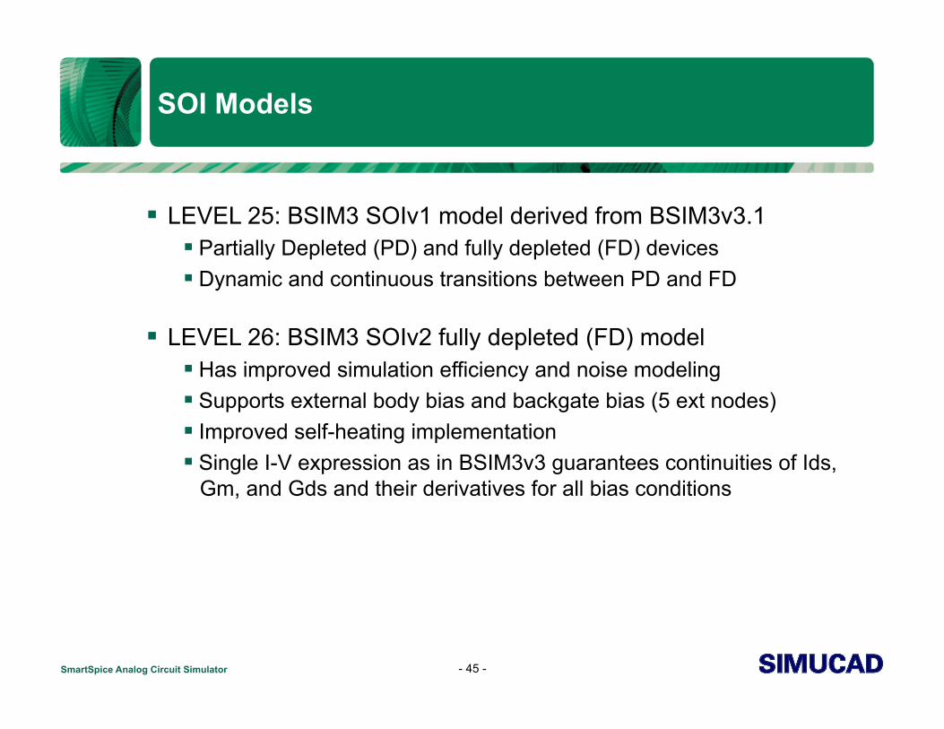
LEVEL 25: BSIM3 SOIv1 model derived from BSIM3v3.1 Partially Depleted (PD) and fully depleted (FD) devices Dynamic and continuous transitions between PD and FD
LEVEL 26: BSIM3 SOIv2 fully depleted (FD) model Has improved simulation efficiency and noise modeling Supports external body bias and backgate bias (5 ext nodes) Improved self-heating implementation Single I-V expression as in BSIM3v3 guarantees continuities of Ids,
Gm, and Gds and their derivatives for all bias conditions
- 45 -
SmartSpice Analog Circuit Simulator
SOI Models (con’t)
LEVEL 27: BSIM3 SOIv2 dynamic depletion (DD) model The dynamic depletion approach is applied on both I-V and C-V Charge and drain current are scalable same features as in LEVEL = 26
LEVEL 29: BSIM3 SOIv2 partially depleted (PD) model Real floating body simulation in both C-V and I-V. The body potential is
determined by the balance of all the body current components Enhancements in the threshold voltage and bulk charge formulation of
the high positive body bias regime An improved parasitic bipolar current model An improved impact ionization current model
- 46 -
SmartSpice Analog Circuit Simulator
SOI Models (con’t)
LEVEL 33 : BSIM3 SOIv3 Includes Partially and Fully depleted models
PD module identical to BSIM3 SOIv2 Improved FD module Ideal Fully Depleted model for strongly FD devices (without floating body
effect) Non Ideal Fully Depleted model Automatic selection among the above modes
New Gate-to-channel and Gate-to-Source/Drain currents New gate resistances model, including RF
- 47 -
SmartSpice Analog Circuit Simulator
SOI Models (con’t)
LEVEL 32: CEA/LETI model (LETISOI) For modeling the static and dynamic electrical behavior of partially-
depleted SOI devices Only uses pure analytical current and charge equations
- 48 -

SmartSpice Analog Circuit Simulator
FRAM Model
Based on original RAMTRON model Three parallel elements: a linear capacitor, a resistor and a current
source Improved scalability with area Improved convergence and accuracy through continuos
derivatives Parameter clipping for convergence Proportion of domains switched
- 49 -

SmartSpice Analog Circuit Simulator
Device Models: Diodes
LEVEL 1: Standard junction diode model (non geometric model)
LEVEL 2: Fowler-Nordheim diode model Created as metal-semiconductor or s-m-s The insulator of this type of diode is very thin (about 100 Å), which
allows for the tunneling of the carriers Modeling electrically-alterable memory cells and other insulation
breakdown devices In many applications, they are in parallel together. The multiplier M is
then used to simplify the simulation
- 50 -
SmartSpice Analog Circuit Simulator
Device Models: Diodes (con’t)
LEVEL 3: Junction diode model (geometric model)
LEVEL 9: Philips JUNCAP diode model LEVEL 500: Philips LEVEL 500 diode model
Forward biasing (ideal current, non ideal current including tunneling) Reverse biasing (Trap assisted tunneling, Shockley-Read-Hall
generation, band-to-band tunneling, avalanche multiplication) Breakdown Series resistances Charge storage effects temperature scaling rules Noise model for RS and the ideal forward current
- 51 -
SmartSpice Analog Circuit Simulator
Device Models: Diodes (con’t)
LEVEL 4: RPI VCSEL laser diode Vertical Cavity Surface Emitting Laser Mixed Electronic/Photonic (MEP) simulation : photonic part described
in terms of equivalent electrical signal. Can be connected to transmission line and optical receiver devices
- 52 -

SmartSpice Analog Circuit Simulator
Device Models: JFETs
LEVEL 1: Basic SPICE model with Sydney University enhancements
LEVEL 2: Modified SPICE model with gate modulation of LAMBDA Takes into consideration the dependence of channel length modulation
on gate voltage (by means of the model parameter LAM1)
- 53 -
SmartSpice Analog Circuit Simulator
Device Models: MESFETs
LEVEL 1: JFET model LEVEL 2: Statz model LEVEL 3: Curtice model LEVEL 4: Curtice-Ettenburg model LEVEL 5: TriQuint model LEVEL 6: Parker Skellern model LEVEL 7: TriQuint-2 model
- 54 -

SmartSpice Analog Circuit Simulator
Passive Elements and Independent Sources
Resistors Capacitors Inductors Mutual inductors and magnetic cores Switches Independent voltage, current, DC, AC, transient or mixed sources
- 55 -

SmartSpice Analog Circuit Simulator
Transmission Lines
Lossless Transmission Line Berkeley Lossy Transmission Line Model Lossy Transmission Line - Recursive Convolution Model W Element - Multiconductor Lossy frequency Dependent
Transmission Line (Under development)
- 56 -
SmartSpice Analog Circuit Simulator
Analog Behavioral Modeling
Analog Behavioral Device Unique SmartSpice device The current through/voltage across can be an arbitrary mathematical
expression referencing node voltage and device current The expression can contain the derivative operator Expressions can contain if…then…else conditions Expressions can access the circuit temperature, current, time and
current timestep(tstep) Delay-type device can be used to model an ideal delay
- 57 -
SmartSpice Analog Circuit Simulator
Controlled Sources
Voltage Controlled Voltage Source Current Controlled Current Source Voltage Controlled Current Source Current Controlled Current Source
- 58 -

SmartSpice Analog Circuit Simulator
Conclusion
The complete set of industry standard models are available Berkley compatible syntax form for quick model implementation Long history of experience with large customer base and diverse
customer applications
- 59 -


![İklimlendirme Alanında Trend ve Teknolojiler [Uyumluluk Modu]°KLİMLENDİRME... · Otomasyonun, iklimlendirme sisteminin etkinliğini arttırırken, işletme gidl dderlerinin düşürüllmesinin](https://img.dokumen.tips/doc/110x75/5e10261503ddd525ae28bfc8/klimlendirme-alannda-trend-ve-teknolojiler-uyumluluk-modu-klmlendrme.jpg)