Embed Size (px)
Citation preview

©iS
toc
kp
ho
to/w
ha
nw
ha
na
iSmart Manufacturing
IEEE PotEntIals July/August 2016 ■ 90278-6648/16©2016IEEE
Smart assembly for soft bioelectronics
Chi Hwan Lee
Biology is soft and curvilin-ear, whereas wafer-based electronics are rigid and planar. The mechanical mismatch impedes the
effective integration of electronic sys-tems with biological tissues or skins, paving the way for the construction of device materials (i.e., semiconduct-ing composites) onto soft, biocompati-ble elastomers with the ability to be stretched, bent, and twisted. Advanc-es in mechanics allow the rather brittle device materials to accommo-date large levels of strain (&1%) and therefore retain their functionality under repeated mechanical deforma-tions in use.
A large array of emerging prod-ucts ranging from skin-like wearable health-monitoring systems to stretch-able, bioresorbable electronic implants exist at a prototyping or commercializ-ing phase. This article reviews recent developments in advanced assembly techniques to integrate various de-vice materials with bio-related soft substrates and their applications in emerging biomedical devices.
advanced assembly techniquesA set of techniques has become available for the assembly of device materials with soft, biocompatible elastomers. A representative strate-gy, often referred to as a transfer printing technique, uses a series of
pick-and-place processes in a deter-ministic manner in which arrays of device materials are picked from a native substrate by using a visco-elastic stamp, such as polydimethy-
lsiloxane (PDMS), and then printed onto a receiver substrate. Various classes of device materials in the forms of membranes, ribbons, or wires are available for the process to
Digital Object Identifier 10.1109/MPOT.2016.2540078 Date of publication: 20 July 2016
ima
ge
lic
en
Se
d b
y in
gr
am
pu
bli
Sh
ing

10 ■ July/August 2016 IEEE PotEntIals
serve as active semiconducting components.
The basic mechanism of the pro-cess relies on the intrinsic viscoelas-tic behavior of the stamps, where the adhesion forces strongly depend on peeling rate; when the stamp delam-inates quickly (>~10 cm/s), the adhe-sion energy at the interface between stamp and device materials is larger than its counterpart at the interface
between the donor substrate and device materials and, thereby, the stamp can “pick-up” the device ma-terials. Similarly, the opposite oc-curs when the stamp delaminates slowly (< ~10 cm/s) for “printing” step. To further enhance the efficacy of the pick-and-place process, sev-eral techniques exploit the modified viscoelastic stamp configured with carefully defined microstructures.
Figure 1 shows an example that uses a viscoelastic stamp with py-ramidal microtips at the corners, allowing pressure-modulated adhe-sion controls in high- and low-ad-hesion states for picking and print-ing successively. The compressed stamp, when in full contact (Fig. 1,
top panel) has a strong rate-depen-dent behavior while the adhesion forces decrease when the stamp re-trieves its original shape (Fig. 1, bot-tom panel). The large differences in contact area allow for the high levels of adhesion switching between the high- and low-adhesion states.
The commercial grade of complete-ly automated tools for the adhesion- controlled pick-and-place processes
over wafer-scale exist with the capa-bilities of printing rates more than millions of device materials per hour, nearly 100% yields, and placement accuracy better than 1 "m. Many of the emerging electronic systems de-scribed in the following sections ex-ploit these techniques and serve as test bed applications of the reliable assembly capabilities.
Other classes of transfer printing techniques also exist in which the basic working principles rely on dif-ferent phenomenon. A representative example includes the environment- assisted transfer printing technique that exploits a controlled interfacial delamination phenomenon by using water in manipulated environments
in terms of temperature, pH, and chemical surfactants.
Here, a layer of ductile metals such as nickel or copper (~ 300 nm thick) serves as the separation layer at the interface between the growth/fabrication substrate and the pre- fabricated device on top. In the pres-ence of water, the applied mechanical peeling forces deforms the chemical bonds of the metal (separation) layer and the surface of the growth/fabri-cation substrate (i.e., a silicon wafer), causing induced electrostatic charg-es to attract water molecules.
Chemical reactions happen be-tween the attracted water molecu-les and the mechanically strained chemical bonds at the debonding tips, thereby significantly reducing the energy release rate (up to ~75%) to readily generate the interfacial delamination. The phenomenon is referred to as water-assisted sub-critical debonding. The resulting in-terfacial delamination liberates the device layer from the growth/fab-rication substrate and then prints onto a receiver “target” substrate to complete the entire process. No post-fabrication steps are required, so the choices of receiver substrates can be extended to almost arbitrary materi-als ranging from paper, rubber, plas-tic, and bio-related soft materials. Demonstration devices enabled by the technique include flexible thin-film solar panels, ultrathin nanosen-sors, wearable memory devices, and water-dissolvable electronic systems. No effective biomedical devices have yet appeared.
One disadvantage involves the fact that the metallic separation layer (nickel or copper) prevents the growth of monocrystalline semiconducting materials, impeding the construc-tion of commercial-grade products. Efforts to overcome this limitation are being exerted.
skin-like wearable electronicsWearable electronic systems that typically consist of an array of sensors, data acquisition modules, and remote control stations have evolved for several decades in diverse forms by exploiting wrists, shirts,
Fig1 Scanning electron microscope (Sem) images of a viscoelastic stamp bearing pyramidal microtips in high- and low-adhesion states [(a) and (c), respectively], in which the transferring object appears green. (b) and (d) show high magnification images of individual microtips in each state.
On 25 µm
5 µm
(a) (b)
Off 25 µm
2 µm
(c) (d)
Advances in mechanics allow the rather brittle device materials to accommodate large levels of
strain (&1%) and therefore retain their functionality under repeated mechanical deformations in use.
IEEE PotEntIals July/August 2016 ■ 11
bands, socks, or adhesive patches. These devices have many important capabilities for applications in at-home health-care systems, but a key challenge remains in the discomfort of unsuitable sizes, weights, and shapes for practical applications during prolonged use.
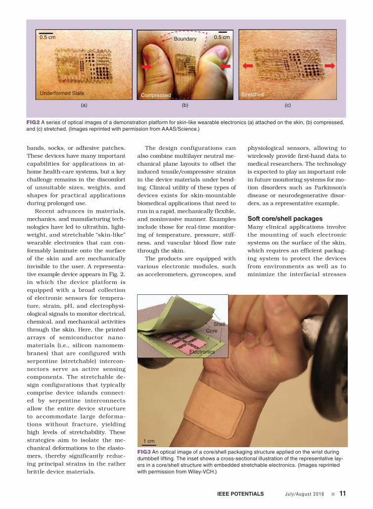
Recent advances in materials, mec hanics, and manufacturing tech -nologies have led to ultrathin, light-weight, and stretchable “skin-like” wearable electronics that can con-formably laminate onto the surface of the skin and are mechanically invisible to the user. A representa-tive example device appears in Fig. 2, in which the device platform is equipped with a broad collection of electronic sensors for tempera-ture, strain, pH, and electrophysi-ological signals to monitor electrical, chemical, and mechanical activities through the skin. Here, the printed arrays of semiconductor nano-materials (i.e., silicon nanomem-branes) that are configured with serpentine (stretchable) intercon-nectors serve as active sensing components. The stretchable de-sign configurations that typically comprise device islands connect-ed by serpentine interconnects allow the entire device structure to accommodate large deforma-tions without fracture, yielding high levels of stretchability. These strateg ies aim to isolate the me-chanical de for mations to the elasto-mers, thereby significantly reduc-ing principal strains in the rather brittle device materials.
The design configurations can also combine multilayer neutral me-chanical plane layouts to offset the induced tensile/compressive strains in the device materials under bend-ing. Clinical utility of these types of devices exists for skin-mountable biomedical applications that need to run in a rapid, mechanically flexible, and noninvasive manner. Examples include those for real-time monitor-ing of temperature, pressure, stiff-ness, and vascular blood flow rate through the skin.
The products are equipped with various electronic modules, such as accelerometers, gyroscopes, and
physiological sensors, allowing to wirelessly provide first-hand data to medical researchers. The technology is expected to play an important role in future monitoring systems for mo-tion disorders such as Parkinson’s disease or neurodegenerative disor-ders, as a representative example.
soft core/shell packagesMany clinical applications involve the mounting of such electronic systems on the surface of the skin, which requires an efficient packag-ing system to protect the devices from environments as well as to minimize the interfacial stresses
0.5 cm
Underformed State Compressed
Boundary 0.5 cm
Stretched
(a) (b) (c)
Fig2 a series of optical images of a demonstration platform for skin-like wearable electronics (a) attached on the skin, (b) compressed, and (c) stretched. (images reprinted with permission from aaaS/Science.)
CoreShell
Electronics
1 cm
Fig3 an optical image of a core/shell packaging structure applied on the wrist during dumbbell lifting. the inset shows a cross-sectional illustration of the representative lay-ers in a core/shell structure with embedded stretchable electronics. (images reprinted with permission from wiley-Vch.)

12 ■ July/August 2016 IEEE PotEntIals
with the skin. Recent approaches have developed core/shell structures (Fig. 3, inset) where the core con-tains the functional devices sur-rounded with either extremely soft liquid or solid materials, while the shell involves a thin enclosure using a different elastomer to pro-vide a robust interface for handling and laminating onto the skin.
A demonstration example exp-loits microfluidic spaces filled with dielectric fluids (i.e., silicone oli-gomer without curing agent) for the core and supporting elastome ric substrate/encapsulate layer (i.e., Ecoflex) for the shell. Devices and as-sociated stretchable interconnectors are suspended in the microfluidic space, where each electronic com-ponent is selectively anchored to the bottom surface. The configura-tion allows for the decoupling of the mechanics of the free-floating inter-connectors from the shell, enabling large-range mo tions with little con-straint in response to externally im-posed de formations, such as bend-ing, stretching, and twisting.
A disadvantage, however, exists in this structure for the possibility of fluid leakage from the damage to the shell. To resolve this issue, an alternative strategy exploits an ul-tralow modulus solid silicone elasto-mer (i.e., Silbione, Young’s modulus (E) = ~5 kPa) for the core material
to capture the favorable mechanics and to eliminate any possibility for the leakage. Here, the thickness of the core material plays a critical role in the mechanical isolation of the devices where the effective tensile modulus of the core/shell package can significantly decrease as the thickness of the core material in-creases. The optimized layout of the
core/shell package yields mechani-cally imperceptible systems to the wearers for normal skin sensitivity (~20 kPa) with abilities of reversible responses to large strain deforma-tions (up to > ~30%).
As shown in Fig. 3, the pack-age structure can also incorporate a human skin-like color by ap-plying a commercial coloring pig-ment to provide aesthetics for the skin-mountable units. The result-ing device can intimately mount onto the surface of the skin with-out delamination, simultaneously allowing for the monitoring of phy siological signals or sense mo-tions of the wearer by exploiting the built-in functionalities.
Bioresorbable electronic implantsEfforts toward mechanically unusu-al forms of electronic systems have established the foundations to advance the technology for even more challenging materials and
devices. Paradigms of the device platforms can shift from wearable, stretchable to implantable, biore-sorbable formats. The latter presents the electronic devices with the abili-ty to physically dissolve via resorp-tion in the body in a programma-ble manner.
The devices, often referred to as transient electronics, consist of en-tirely biocompatible and bioresorb-able materials, as well as nontoxic end products, such as magnesium/molybdenum for conductors, sili-con dioxides/magnesium oxide for dielectrics and passivation layers, single crystalline silicon nanomem-branes for semiconductors, and silk/poly( lactic-co-glycolic acid) for substrates and encapsulating ma-terials. The resulting outcome pres-ents the integrated circuits that can temporarily provide diagnostic and/or therapeutic functions, followed by complete dissolution in the body at a prescribed time frame, thereby eliminating the unnecessary load for surgical extraction of the implan-ted hardware.
Figure 4 shows the first proof- of-concept device, pioneered by Prof. John A. Rogers’ group at the Univer-sity of Illinois at Urbana–Champaign, that comprises a set of electronic components, ranging from inductors, capacitors, resistors, diodes, transis-tors, and metal interconnects, to sub-strate/encapsulate, all in a complete-ly dissolvable format by deionized water at room temperature. Mechani-cal stretchability for these classes of devices is also important, especially when they serve as implantable sys-tems by integrating with the curvilin-ear surfaces of biological tissues.
1 cm
0 min 5 min 10 min
Fig4 a series of optical images of a demonstration platform for bioresorbable (transient) electronics dissolved in deionized water in time sequence. (images reprinted with permission from aaaS/Science.)
Efforts toward mechanically unusual forms of electronic systems have established the foundations to advance the technology for even more challenging
materials and devices.

IEEE PotEntIals July/August 2016 ■ 13
For this purpose, the devices can incorporate the stretchable design configurations, such as device is-lands connected with serpentine in-terconnects to accommodate various levels of strains. Example devices show stretchability up to ~30% with-out degradations in performances, where portions of the device struc-tures begin to delaminate when fur-ther stretched.
The demonstration examples in-volve stretchable, bioresorbable pH monitors where the chemically func-tionalized silicon nanoribbons serve as an active sensing element to de-tect the change of pH of surrounding aqueous solutions. Here, dissolvable metals such as magnesium serves as the electrodes and interconnects, silicon dioxide serve as the interlay-er dielectrics and encapsulant, and biodegradable elastomer (poly-1,8-octanediol-co-citrate) serves as the substrate. Each component com-pletely dissolves within hours to days in physiological conditions (i.e., phosphate buffer saline, pH: ~7.4 at 37 °C) via reactive resorptions (hy-drolysis). In the same condition, the conductance of sensing materials (i.e., doped silicon nanoribbons) is changed by only ~1% or less during immersion for five days. The dis-solution behaviors are tunable de-pending on materials, thicknesses, morphologies, and encapsulation strategies. Essential concepts, ba-sic materials, and fabrication tech-niques are now available for these types of technology.
ConclusionAdvanced materials, assembly tech-niques, soft core/shell packaging strategies, and stretchable mechan-ics designs have established a route to build new classes of soft bioelec-tronics with capabilities that can-not be achieved by conventional electronic systems. Emerging elec-tronic systems enabled by these technologies were reviewed includ-ing skin-like wearable electronics and bioresorbable electronic im -plants. The monolithic integrated
systems equipped with wireless power suppliers and data commu-nications are continuously improv-ing. Interesting future topics in the relevant research includes the in -vestigations of possible interactions through the effective interface between the soft bioelectronics and the surrounding biology.
Read more about it • M. A. Meitl, Z. T. Zhu, V.
Kumar, K. J. Lee, X. Feng, Y. Y. Huang, I. Adesida, R. G. Nuzzo, and J. A. Rogers, “Transfer printing by kinetic control of adhesion to an elastomeric stamp,” Nat. Mater., vol. 5, pp. 33–38, 2006.
• D. H. Kim, N. Lu, R. Ma, Y. S. Kim, R. H. Kim, S. Wang, J. Wu, S. M. Won, H. Tao, A. Islam, K. J. Yu, T. I. Kim, R. Chowdhury, M. Ying, L. Xu, M. Li, H. J. Chung, H. Keum, M. McCormick, P. Liu, Y. W. Zhang, F. G. Omenetto, Y. Huang, T. Coleman, and J. A. Rogers, “Epidermal elec-tronics,” Science, vol. 333, pp. 838–843, 2011.
• A. Carlson, A. M. Bowen, Y. Huang, R. G. Nuzzo, and J. A. Rog-ers, “Transfer printing techniques for materials assembly and micro/nanodevice fabrication,” Adv. Mater., vol. 24, pp. 5284–5318, 2012.
• S. W. Hwang, H. Tao, D. H. Kim, H. Cheng, J. K. Song, E. Rill, M. A. Brenckle, B. Panilaitis, S. M. Won, Y. S. Kim, Y. M. Song, K. J. Yu, A. Ameen, R. Li, Y. Su, M. Yang, D. L. Kaplan, M. R. Zakin, M. J. Slepi-an, Y. Huang, F. G. Omenetto, and J. A. Rogers, “A physically transient form of silicon electronics,” Science, vol. 337, pp. 1640–1644, 2012.
• C. H. Lee, D. Kim, I. Cho, N. William, Q. Wang, and X. Zheng, “Peel-and-stick: Fabricating thin- film solar cell on universal sub-strates,” Sci. Rep., vol. 2, pp. 1000, 2012.
• S. W. Hwang, D. H. Kim, H. Tao, T. I. Kim, S. Kim, K. J. Yu, B. Panilaitis, J. W. Jeong, J. K. Song, F. G. Omenetto, and J. A. Rogers, “Materials and fabrication processes for transient and bioresorbable high-
performance electronics,” Adv. Funct. Mater., vol. 23, pp. 4087–4093, 2013.
• C. H. Lee, J. Kim, C. Zou, I. Cho, J. Weisse, W. Nemeth, Q. Wang, A. Duin, T. Kim, and X. Zheng, “Peel-and-stick: Mechanism study for effi-cient fabrication of flexible/transpar-ent thin- film electronics,” Sci. Rep., vol. 3, pp. 2917, 2013.
• S. W. Hwang, G. Park, H. Cheng, J. K. Song, S. K. Kang, L. Yin, J. H. Kim, F. G. Omenetto, Y. Huang, K. M. Lee, and J. A. Rogers, “25th anniversary article: Materials for high-performance biodegradable semiconductor devices,” Adv. Mater., vol. 26, pp. 1992–2000, 2014.
• C. H. Lee, D. Kim, and X. Zheng, “Transfer printing processes for thin-film solar cells: Basic con-cepts and working principles,” ACS Nano, vol. 8, pp. 8746, 2014.
• C. H. Lee, Y. Ma, K. I. Jang, A. Banks, T. Pan, X. Feng, J. S. Kim, D. Kang, M. S. Raj, B. L. McGrane, B. Morey, X. Wang, R. Ghaffari, Y. Huang, and J. A. Rogers, “Soft core/shell packages for stretchable elec-tronics,” Adv. Funct. Mater., vol. 25, pp. 3698–3704, 2015.
• C. H. Lee, Y. Ma, K. I. Jang, A. Banks, T. Pan, X. Feng, J. S. Kim, D. Kang, M. S. Raj, B. L. McGrane, B. Morey, X. Wang, R. Ghaffari, Y. Huang, and J. A. Rogers, “Soft core/shell packages for stretchable elec-tronics,” Adv. Funct. Mater., vol. 25, pp. 3698–3704, 2015.
about the authorChi Hwan Lee ([email protected]) is currently an assistant professor at Purdue University, with appoint-ments in the Weldon School of Bio-medical Engineering and the School of Mechanical Engineering. He earned dual B.S. degrees from Illinois Institute of Technology and Ajou Uni-versity, Korea, in 2007 with double majors in mechanical engineering and industrial engineering. He also earned M.S. and Ph.D. degrees in mechanical engineering from Stan-ford University in 2013.