Embed Size (px)
Citation preview

Small Area Power Converter for Application to Distributed On-Chip Power Delivery
Eby
G. Friedman

Agenda
Motivation
Point-of-load voltage regulator
Distributed on-chip power delivery
Distributed 3-D rectifier
Conclusions
2

Agenda
Motivation
Point-of-load voltage regulator
Distributed on-chip power delivery
Distributed 3-D rectifier
Conclusions
3

Power Delivery in Modern ICsTypical power delivery
4
Typical power delivery
Off-chip power supplies provide current
Low quality voltage regulation
Slower response time
IR
and Ldi/dt
voltage drops
Large number of dedicated I/O pads
Increases with the number of voltage domains

Power Delivery in Modern ICsTypical power delivery
5
On-chip power delivery
On-chip power delivery
Multi-supply voltage processors
Need higher efficiency
Reduced parasitic impedances
Enhanced voltage regulation
Smaller parasitic voltage drops
Faster load regulation
Size of existing on-chip supplies is large
Small voltage regulators are required

Power Delivery in Modern ICsTypical power delivery
6
On-chip power delivery
Proposed power delivery
Proposed power delivery
Smaller on-chip power supplies
Fast algorithms for power grid analysis
More efficient design and analysis of highly complex circuits
Design methodology for simultaneously placing decoupling capacitors and distributed power supplies
Enhanced load regulation
Point-of-load voltage regulation
Increased power efficiency of overall system
Agenda
Motivation
Point-of-load voltage regulator
Distributed on-chip power delivery
Distributed 3-D rectifier
Conclusions
7

Typical On-Chip Voltage Regulation
Existing on-chip power supplies
Large on-chip area requirement
Difficult to implement multiple voltage domains
Several power supplies are required
Slow response time
Parasitic impedances degrade response time
High parasitic voltage drop
Power supplies are far from the load circuitry
Large parasitic impedance between power supply and load circuits
8
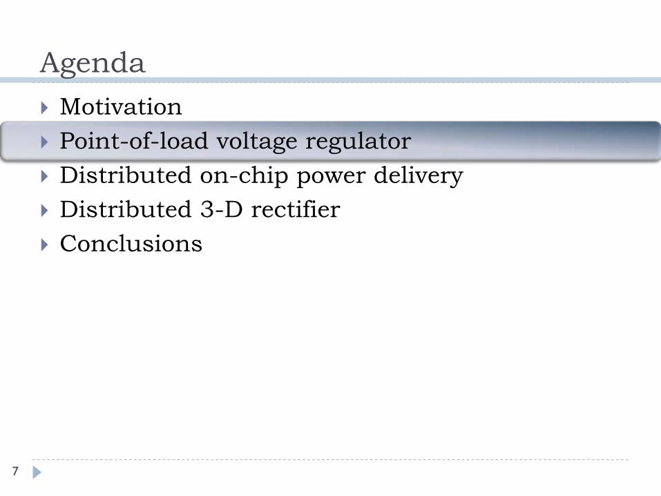
Point-of-Load Voltage Regulation
Small local point-of-load power supplies solve these problems
Small on-chip area
Fast response time and low parasitic voltage drop
Small parasitic impedance between power supply and load circuitry
Voltage is generated close to the load circuitry
More robust voltage regulation
Small output DC voltage shift for different current demands
Maximum output current demand of each power supply is small
9
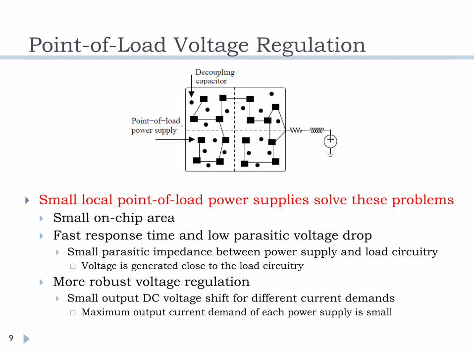
Feedback–Active Filter Based Converter
Op-amp
Load Circuits
Vdd2
R1 R3R2
C2
C3C1
Vdd1
PWM
Feedback
2nd
feedback
10

Choice of Filter Topology
Filter types
Butterworth
Chebyshev
type I
Bessel
Chebyshev
type II
Elliptic
…
Filter configurations
Sallen-Key
No DC current path
From input to output
To the ground
Multiple feedback
DC current path between input and output
No DC current path to ground
Twin-t and bridged-t feedback
DC current path from input to output
DC current path to ground
…
Zeroes at infinity
Finitezeroes
Chebyshev
type I
Faster transition than Butterworth and Bessel
No zeros needed in the transfer function
Sallen-Key configuration is used
No DC current pathº
Minimize the static power dissipation
11
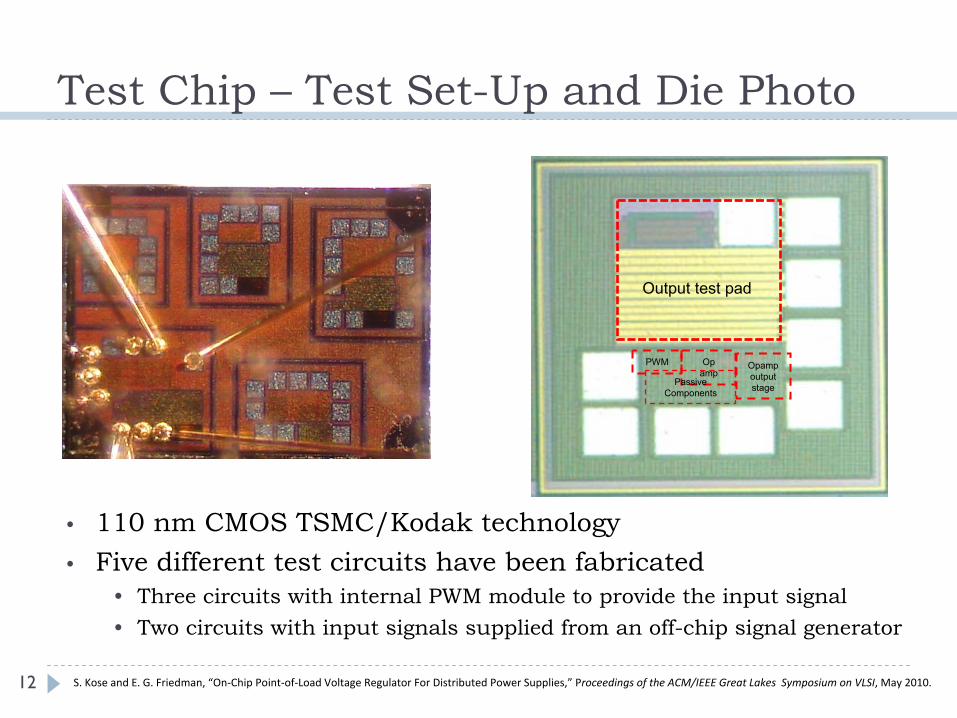
Test Chip –
Test Set-Up and Die Photo
Op amp
Passive Components
Output test pad
PWM Opamp
output stage
•
110 nm CMOS TSMC/Kodak technology•
Five different test circuits have been fabricated•
Three circuits with internal PWM module to provide the input signal•
Two circuits with input signals supplied from an off-chip signal generator
S. Kose
and E. G. Friedman, “On‐Chip Point‐of‐Load Voltage Regulator For Distributed Power Supplies,”
Proceedings of the ACM/IEEE Great Lakes Symposium on VLSI, May 2010.12
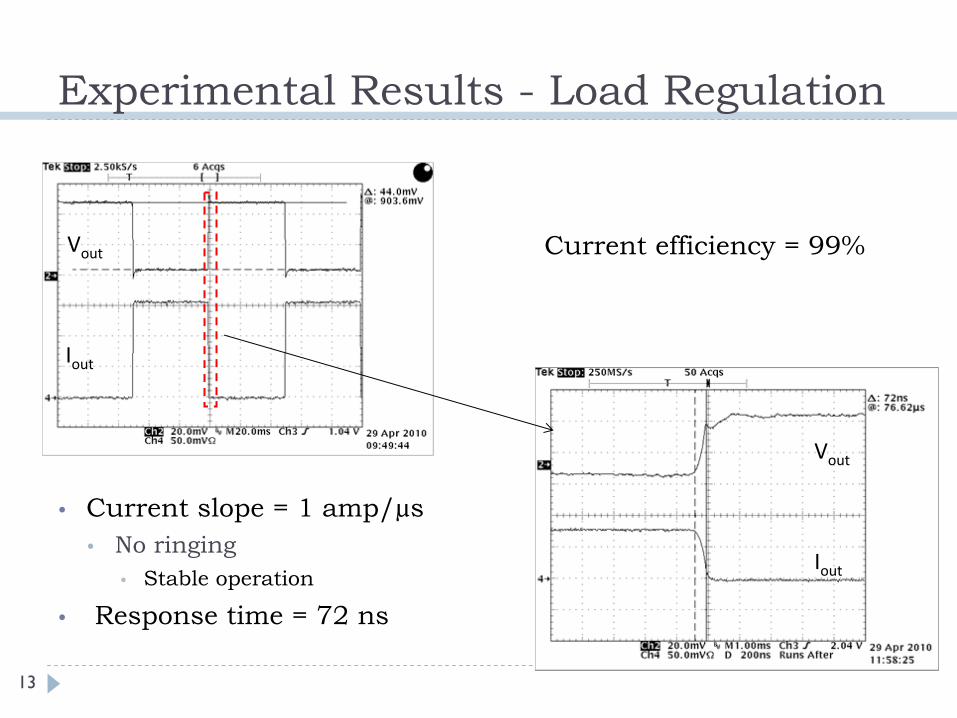
Experimental Results -
Load Regulation
•
Current slope = 1 amp/µs•
No ringing•
Stable operation
•
Response time = 72 ns
13
Current efficiency = 99%Vout
Iout
Vout
Iout
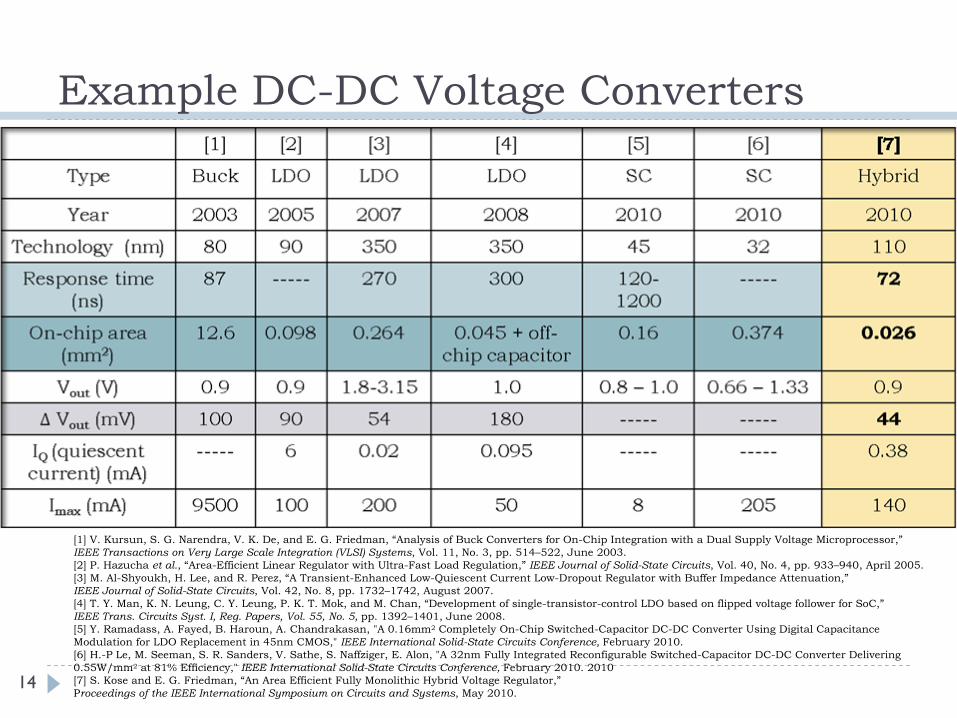
Example DC-DC Voltage Converters
[1] V. Kursun, S. G. Narendra, V. K. De, and E. G. Friedman, “Analysis of Buck Converters for On-Chip Integration with a Dual Supply Voltage Microprocessor,”
IEEE Transactions on Very Large Scale Integration (VLSI) Systems, Vol. 11, No. 3, pp. 514–522, June 2003.[2] P. Hazucha
et al., “Area-Efficient Linear Regulator with Ultra-Fast Load Regulation,”
IEEE Journal of Solid-State Circuits, Vol. 40, No. 4, pp. 933–940, April 2005.[3] M. Al-Shyoukh, H. Lee, and R. Perez, “A Transient-Enhanced Low-Quiescent Current Low-Dropout Regulator with Buffer Impedance Attenuation,”IEEE Journal of Solid-State Circuits, Vol. 42, No. 8, pp. 1732–1742, August 2007.[4] T. Y. Man, K. N. Leung, C. Y. Leung, P. K. T. Mok, and M. Chan, “Development of single-transistor-control LDO based on flipped voltage follower for SoC,”IEEE Trans. Circuits Syst. I, Reg. Papers, Vol. 55, No. 5, pp. 1392–1401, June 2008.[5] Y. Ramadass, A. Fayed, B. Haroun, A. Chandrakasan, "A 0.16mm2
Completely On-Chip Switched-Capacitor DC-DC Converter Using Digital Capacitance Modulation for LDO Replacement in 45nm CMOS," IEEE International
Solid-State Circuits Conference, February 2010.[6] H.-P Le, M. Seeman, S. R. Sanders, V. Sathe, S. Naffziger, E. Alon, "A 32nm Fully Integrated Reconfigurable Switched-Capacitor DC-DC Converter Delivering 0.55W/mm2
at 81% Efficiency," IEEE International
Solid-State Circuits Conference, February 2010. 2010[7] S. Kose
and E. G. Friedman, “An Area Efficient Fully Monolithic Hybrid Voltage Regulator,”Proceedings of the IEEE International Symposium on Circuits and Systems, May 2010.
14

Agenda
Motivation
Point-of-load voltage regulator
Distributed on-chip power delivery
Distributed 3-D rectifier
Conclusions
15
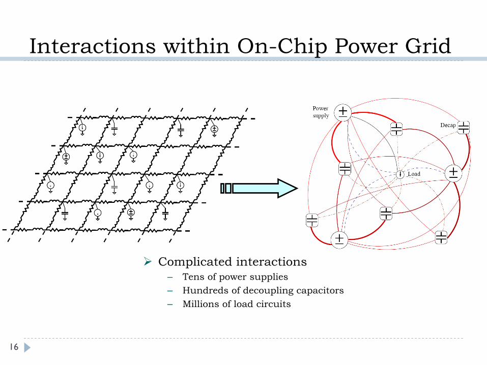
Interactions within On-Chip Power Grid
16
Complicated interactions–
Tens of power supplies–
Hundreds of decoupling capacitors–
Millions of load circuits
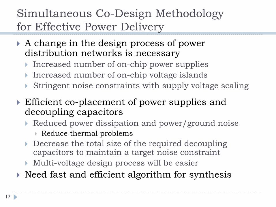
Simultaneous Co-Design Methodology for Effective Power Delivery
17
A change in the design process of power distribution networks is necessary
Increased number of on-chip power supplies
Increased number of on-chip voltage islands
Stringent noise constraints with supply voltage scaling
Efficient co-placement of power supplies and decoupling capacitors
Reduced power dissipation and power/ground noise
Reduce thermal problems
Decrease the total size of the required decoupling capacitors to maintain a target noise constraint
Multi-voltage design process will be easier
Need fast and efficient algorithm for synthesis

Closed-Form Expressions of Effective Impedance
dmeneRnm
BA
)sinh(
))cos()cos(2( ||||
),(
51469.0)ln(21 22
),( mnR BA
(x1
, y1
)
(x2
,y2
)
R
R
Infinite uniform resistive grid
Identical resistance, R
Models power or ground distribution network
Effective resistance between arbitrary points is utilized in power grid analysis
A
B
|-y|xn| -x|xmwhere 2221 and Exact solution*
Asymptotic solution*
*G. Venezian, “On the Resistance between Two Points on a Grid,”
American Journal of Physics, Vol. 62, No. 11, pp. 1000–1004, November 1994.
– Maximum error < 3% (for an adjacent node)
18

Point-of-Load Supply vs. Decoupling Capacitance
19
Developed fast algorithm for power grid analysis
Reduces the time required to optimize the locations of multiple power supplies and decoupling capacitors
Considers physical distance among circuit components and power grid characteristics in the co-placement methodology
Incorporates the distinctive properties of the power supplies and decoupling capacitors
On-chip power supply On-chip decoupling capacitor
Area Greater area requirement
Smaller
area requirement
Response time Slower response Faster
response
Power efficiency Limited efficiency due to the active devices and parasitic impedances
Power loss only
due to parasitic impedances
Maximum supplied current
High Limited to the size of the capacitor. Decay and recharge rate of the capacitor should be considered
V. Kursun
and E. G. Friedman, Multi‐Voltage CMOS Design, New York: Wiley, 2006.
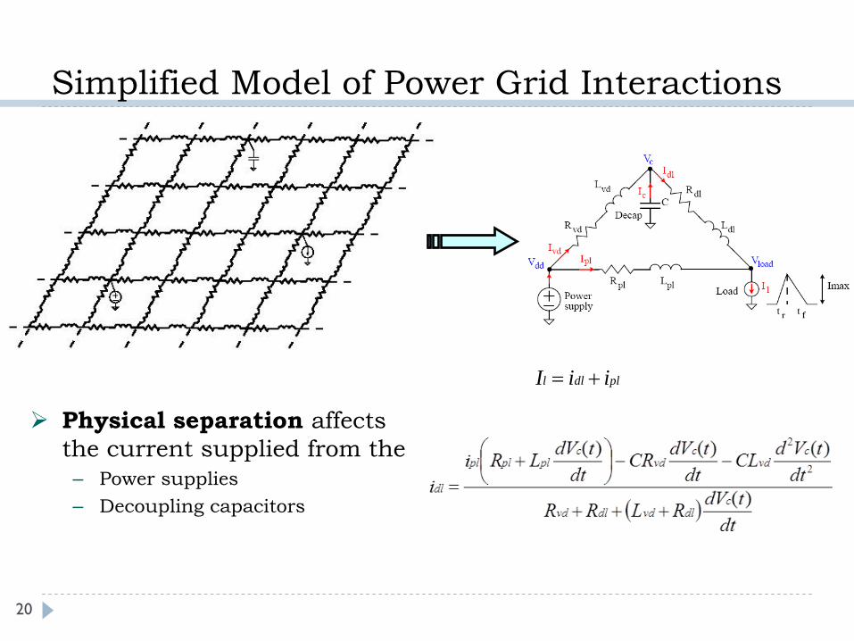
Simplified Model of Power Grid Interactions
Physical separation affects the current supplied from the
–
Power supplies–
Decoupling capacitors dt
tdVRLRR
dttVdCL
dttdVCR
dttdVLRi
ic
dlvddlvd
cvd
cvd
cplplpl
dl )(
)()()(2
2
pldll iiI
20

Effective Region of Influence of Power Sources
Effective region of one power supply and one decoupling capacitor
Effective regions of one power supply and multiple decoupling capacitors
Effective region exhibits elliptic shape
Long radius is determined by the effective impedance among components
),(),( 1111*
*
yxyxl LkR
CKr
21

Elliptic Shape of Effective Region
22
Power supply
Connected at N(10,10)
Four decoupling capacitors
Connected at N(6,14)
, N(17,17)
, N(5,5)
, and N(18,2)
Load current
Uniformly distributed
tr
100 ps
tf
300 ps
SPICE simulation
Analytic model
Error < 5 %
2.1/ 42 ll rr
15.1/ 42 ll rr

Effect of Load Characteristics on Effective Region
23
tr
-
10 ps, tr
-
30 ps tr
-
50 ps, tf
-150 ps
Four power supplies
Connected at N(3,10)
, N(10,3)
, N(10,17)
, and N(16,10)
Five decoupling capacitors
Connected at N(3,3)
, N(3,17)
, N(10,10)
, N(17,3)
, and N(17,17)
Effective regions strongly depend on
Transition times of load devices
Decoupling capacitors are more effective
When transition time of load current is faster
On-chip power supplies are more effective
When transition times are slower

Agenda
Motivation
Point-of-load voltage regulator
Distributed on-chip power delivery
Distributed 3-D rectifier
Conclusions
24

On-Chip Power Delivery in 3-D Circuits
25
Specialized circuits for integrated power supply within 3-D structures

Distributed 3-D Rectifier
26
Exploits the rectifier portion of a buck converter
Generates and distributes power supplies in 3-D integrated circuits
Eliminates the need for on-chip inductors
Rectifier is composed of transmission lines
Terminated with lumped capacitances
Inter-plane structure is connected by 3-D vias
Low pass behavior
RC-like characteristics

Transfer Function Comparison
27
►
Both filters exhibit similar characteristics in the MHz frequency range►
LC
filter►
Inductor ESR►
Output resistance of power MOSFETs
►
Distributed filter►
Interconnect resistance►
Output resistance of power MOSFETs
►
Multiple poles due to distributed nature of the filter
►
Simultaneous current distribution and signal filtering
-20 dB/Decade
-100 dB/Decade
-40 dB/Decade

Rectifier Design
28
5% voltage ripple
Equal interconnect lengths on each plane
Equal capacitors on each plane
Length = 1 mm
100 lines in parallel
C = 4.2 nF/plane
10 fF/μm2
Area
0.42 mm2/plane
Vpp
= 4.4% of Vdd2

Schematic of Distributed 3-D Rectifier
29
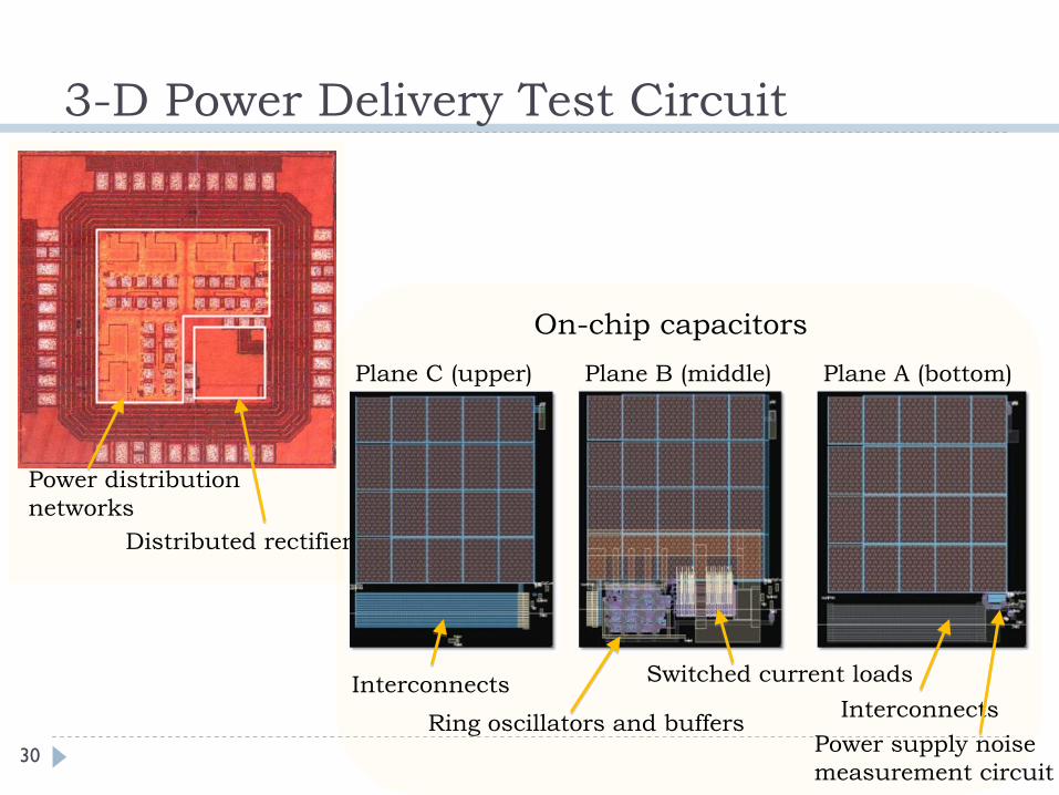
3-D Power Delivery Test Circuit
30
Plane C (upper) Plane B (middle) Plane A (bottom)
On-chip capacitors
InterconnectsInterconnectsRing oscillators and buffers
Switched current loads
Power supply noise measurement circuit
Distributed rectifier
Power distribution networks

Density of On-Chip Capacitance
31
Capacitive density
10 fF/μm2 in the MITLL 150 nm 3-D technology
Increases with technology
Circuit area is reduced to 0.08 mm2

Agenda
Motivation
Point-of-load voltage regulator
Distributed on-chip power delivery
Distributed 3-D rectifier
Conclusions
32

Conclusions
33
An ultra-area efficient on-chip voltage regulator appropriate for point-of-load implementation
0.026 mm2
on-chip area
> 99% current efficiency
Fast response time, 72 ns
Low DC voltage shift, 44 mV (< 5%)
At maximum current demand
Simultaneous co-placement of point-of-load local power supplies and decoupling capacitors
Exploits similarities and differences between power supplies and
decoupling capacitors
Determines the effectiveness regions considering
Physical distances among components
Power/ground parasitic impedances
Work in progress
Distributed power supply for 3-D ICs
Exploits the distributed passive filter and TSVs
within a 3-D system
Currently in test


![[인쇄용] CT6-4 V1 CONVERTER Rev1.7 KOR(2019-06-17) · Manufactured by Distributed by MICROCITY Capacitive Touch Converter Menual CT6-4 V1 2019 - 06 - 17 모델명 최신 펌웨어](https://img.dokumen.tips/doc/110x75/5e5695fed2431c6fd72cc8aa/-ct6-4-v1-converter-rev17-kor2019-06-17-manufactured-by-distributed.jpg)