Embed Size (px)
Citation preview

SGUS044−JULY 2003
1POST OFFICE BOX 1443 • HOUSTON, TEXAS 77251−1443
Controlled Baseline− One Assembly/Test Site, One Fabrication
Site
Extended Temperature Performance of−40°C to 105°C
Enhanced Diminishing ManufacturingSources (DMS) Support
Enhanced Product-Change Notification
Qualification Pedigree †
High-Performance Fixed-Point DigitalSignal Processors (DSPs)−SM320C62x − 5-ns Instruction Cycle Time− 200-MHz Clock Rate− Eight 32-Bit Instructions/Cycle− 1600 MIPS
VelociTI Advanced Very-Long-Instruction-Word (VLIW) C62x DSP Core− Eight Highly Independent Functional
Units:− Six ALUs (32-/40-Bit)− Two 16-Bit Multipliers (32-Bit Result)
− Load-Store Architecture With 32 32-BitGeneral-Purpose Registers
− Instruction Packing Reduces Code Size− All Instructions Conditional
Instruction Set Features− Byte-Addressable (8-, 16-, 32-Bit Data)− 8-Bit Overflow Protection− Saturation− Bit-Field Extract, Set, Clear− Bit-Counting− Normalization
Four-Channel BootloadingDirect-Memory-Access (DMA) ControllerWith an Auxiliary Channel
Flexible Phase-Locked-Loop (PLL) ClockGenerator
3M-Bit On-Chip SRAM− 2M-Bit Internal Program/Cache
(64K 32-Bit Instructions)− 1M-Bit Dual-Access Internal Data
(128K Bytes)− Organized as Two 64K-Byte Blocks for
Improved Concurrency
32-Bit External Memory Interface (EMIF)− Glueless Interface to Synchronous
Memories: SDRAM or SBSRAM− Glueless Interface to Asynchronous
Memories: SRAM and EPROM− 52M-Byte Addressable External Memory
Space
32-Bit Expansion Bus (XBus)− Glueless/Low-Glue Interface to Popular
PCI Bridge Chips− Glueless/Low-Glue Interface to Popular
Synchronous or AsynchronousMicroprocessor Buses
− Master/Slave Functionality− Glueless Interface to Synchronous FIFOs
and Asynchronous Peripherals
Three Multichannel Buffered Serial Ports(McBSPs)− Direct Interface to T1/E1, MVIP, SCSA
Framers− ST-Bus-Switching Compatible− Up to 256 Channels Each− AC97-Compatible− Serial-Peripheral Interface (SPI)
Compatible (Motorola )
Two 32-Bit General-Purpose Timers
IEEE-1149.1 (JTAG‡)Boundary-Scan-Compatible
352-Pin BGA Package (GJL)
0.18-µm/5-Level Metal Process− CMOS Technology
3.3-V I/Os, 1.8-V Internal
!"# $"%&! '#('"! ! $#!! $# )# # #* "#'' +,( '"! $!#- '# #!#&, !&"'##- && $##(
Please be aware that an important notice concerning availability, standard warranty, and use in critical applications ofTexas Instruments semiconductor products and disclaimers thereto appears at the end of this data sheet.
SM320C62x, VelociTI, and C62x are trademarks of Texas Instruments.Motorola is a trademark of Motorola, Inc.Other trademarks are the property of their respective owners.† Component qualification in accordance with JEDEC and industry standards to ensure reliable operation over an extended temperature range.
This includes, but is not limited to, Highly Accelerated Stress Test (HAST) or biased 85/85, temperature cycle, autoclave or unbiased HAST,electromigration, bond intermetallic life, and mold compound life. Such qualification testing should not be viewed as justifying use of thiscomponent beyond specified performance and environmental limits.
‡ IEEE Standard 1149.1-1990 Standard-Test-Access Port and Boundary Scan Architecture.
Copyright 2003, Texas Instruments Incorporated

SGUS044−JULY 2003
2 POST OFFICE BOX 1443 • HOUSTON, TEXAS 77251−1443
Table of Contents
parameter measurement information 38. . . . . . . . . . . . . . . signal transition levels 38. . . . . . . . . . . . . . . . . . . . . . . . . . timing parameters and board routing analysis 39. . . . . .
input and output clocks 40. . . . . . . . . . . . . . . . . . . . . . . . . . .
asynchronous memory timing 42. . . . . . . . . . . . . . . . . . . . .
synchronous-burst memory timing 46. . . . . . . . . . . . . . . . .
synchronous DRAM timing 48. . . . . . . . . . . . . . . . . . . . . . . .
HOLD/HOLDA timing 52. . . . . . . . . . . . . . . . . . . . . . . . . . . .
reset timing 53. . . . . . . . . . . . . . . . . . . . . . . . . . . . . . . . . . . . .
external interrupt timing 55. . . . . . . . . . . . . . . . . . . . . . . . . .
expansion bus synchronous FIFO timing 56. . . . . . . . . . . .
expansion bus asynchronous peripheral timing 58. . . . . .
expansion bus synchronous host-port timing 61. . . . . . . .
expansion bus asynchronous host-port timing 67. . . . . . .
XHOLD/XHOLDA timing 69. . . . . . . . . . . . . . . . . . . . . . . . . .
multichannel buffered serial port timing 70. . . . . . . . . . . . .
DMAC, timer, power-down timing 78. . . . . . . . . . . . . . . . . .
JTAG test-port timing 79. . . . . . . . . . . . . . . . . . . . . . . . . . . .
mechanical data 80. . . . . . . . . . . . . . . . . . . . . . . . . . . . . . . . .
GJL package 2. . . . . . . . . . . . . . . . . . . . . . . . . . . . . . . . . . . . . description 3. . . . . . . . . . . . . . . . . . . . . . . . . . . . . . . . . . . . . . . device characteristics 3. . . . . . . . . . . . . . . . . . . . . . . . . . . . . . C62x device compatibility 5. . . . . . . . . . . . . . . . . . . . . . . . . . . functional and CPU (DSP core) block diagram 6. . . . . . . . . CPU (DSP core) description 7. . . . . . . . . . . . . . . . . . . . . . . . memory map summary 9. . . . . . . . . . . . . . . . . . . . . . . . . . . . . peripheral register descriptions 10. . . . . . . . . . . . . . . . . . . . . DMA synchronization events 14. . . . . . . . . . . . . . . . . . . . . . . interrupt sources and interrupt selector 15. . . . . . . . . . . . . . signal groups description 16. . . . . . . . . . . . . . . . . . . . . . . . . . signal descriptions 19. . . . . . . . . . . . . . . . . . . . . . . . . . . . . . . . development support 30. . . . . . . . . . . . . . . . . . . . . . . . . . . . . . documentation support 33. . . . . . . . . . . . . . . . . . . . . . . . . . . . clock PLL 34. . . . . . . . . . . . . . . . . . . . . . . . . . . . . . . . . . . . . . . power-supply sequencing 35. . . . . . . . . . . . . . . . . . . . . . . . . . IEEE 1149.1 JTAG compatibility statement 36. . . . . . . . . . . absolute maximum ratings over operating case
temperature ranges 37. . . . . . . . . . . . . . . . . . . . . . . . . . recommended operating conditions 37. . . . . . . . . . . . . . . . . electrical characteristics over recommended ranges
of supply voltage and operating case temperature 37
GJL package
GJL 352-PIN BALL GRID ARRAY (BGA) PACKAGE (BOTTOM VIEW)
AF
AD
ABAA
AC
WY
UV
AE
R
NP
L
HJK
M
FG
DE
BA
C
T
252622
2320
19 2117151612
1314 1810
98
7564
32
1 1124

SGUS044−JULY 2003
3POST OFFICE BOX 1443 • HOUSTON, TEXAS 77251−1443
description
The SM320C6202 device is part of the TMS320C62x fixed-point DSP generation in the TMS320C6000 DSPplatform. The C62x DSP devices are based on the high-performance, advanced VelociTIvery-long-instruction-word (VLIW) architecture developed by Texas Instruments (TI), making these DSPs anexcellent choice for multichannel and multifunction applications.
The SM320C62x DSP offers cost-effective solutions to high-performance DSP-programming challenges. TheSM320C6202 has a performance capability of up to 1600 million instructions per second (MIPS) at 200 MHz.The C6202 DSP possesses the operational flexibility of high-speed controllers and the numerical capability ofarray processors. These processors have 32 general-purpose registers of 32-bit word length and eight highlyindependent functional units. The eight functional units provide six arithmetic logic units (ALUs) for a highdegree of parallelism and two 16-bit multipliers for a 32-bit result. The C6202 can produce twomultiply-accumulates (MACs) per cycle. This gives a total of 600 million MACs per second (MMACS) for theC6202 device. The C6202 DSP also has application-specific hardware logic, on-chip memory, and additionalon-chip peripherals.
The C6202 device program memory consists of two blocks, with a 128K-byte block configured asmemory-mapped program space, and the other 128K-byte block user-configurable as cache ormemory-mapped program space. Data memory for the C6202 consists of two 64K-byte blocks of RAM.
The C6202 device has a powerful and diverse set of peripherals. The peripheral set includes three multichannelbuffered serial ports (McBSPs), two general-purpose timers, a 32-bit expansion bus (XBus) that offers ease ofinterface to synchronous or asynchronous industry-standard host bus protocols, and a glueless 32-bit externalmemory interface (EMIF) capable of interfacing to SDRAM or SBSRAM and asynchronous peripherals.
The C62x devices have a complete set of development tools which includes: a new C compiler, an assemblyoptimizer to simplify programming and scheduling, and a Windows debugger interface for visibility into sourcecode execution.
device characteristics Table 1 provides an overview of the 320C6202, 320C6203B, and the 320C6204 pin-compatible DSPs. Thetable shows significant features of each device, including the capacity of on-chip RAM, the peripherals, theexecution time, and the package type with pin count, etc. This data sheet primarily focuses on the functionalityof the SM320C6202 device. For the functionality information on the 320C6203B device, see theTMS320C6203B Fixed-Point Digital Signal Processor data sheet (literature number SPRS086). For thefunctionality information on the 320C6204 device, see the TMS320C6204 Fixed-Point Digital Signal Processordata sheet (literature number SPRS152). And for more details on the C6000 DSP device part numbers andpart numbering, see Table 14 and Figure 4.
TMS320C6000 is a trademark of Texas Instruments.C6000 is a trademark of Texas Instruments.Windows is a registered trademark of the Microsoft Corporation.

SGUS044−JULY 2003
4 POST OFFICE BOX 1443 • HOUSTON, TEXAS 77251−1443
device characteristics (continued)
Table 1. Characteristics of the Pin-Compatible DSPs
HARDWARE FEATURES C6202 C6203B C6204
EMIF √ √ √
Peripherals
DMA 4-Channel4-Channel With
ThroughputEnhancements
4-Channel WithThroughput
EnhancementsPeripheralsExpansion Bus √ √ √
McBSPs 3 3 2
32-Bit Timers 2 2 2
Size (Bytes) 256K 384K 64K
Internal ProgramMemory Organization
Block 0:128K-ByteMapped ProgramBlock 1:128K-ByteCache/MappedProgram
Block 0:256K-Byte MappedProgramBlock 1:128K-ByteCache/MappedProgram
1 Block:64K-ByteCache/MappedProgram
Size (Bytes) 128K 512K 64K
Internal Data MemoryOrganization
2 Blocks:Four 16-Bit Banksper Block50/50 Split
2 Blocks:Four 16-Bit Banksper Block50/50 Split
2 Blocks:Four 16-Bit Banksper Block50/50 Split
CPU ID + CPU Rev ID Control Status Register (CSR.[31:16]) 0x0002 0x0003 0x0003
Frequency MHz 200, 250 250, 300 200
Cycle Time ns4 ns (6202-250)5 ns (6202-200)
3.33 ns (6203B-300)4 ns (6203B-250)4 ns (03BGNZA-250)
5 ns (6204-200)
Core (V) 1.81.5
1.5Voltage
Core (V) 1.81.7
1.5Voltage
I/O (V) 3.3 3.3 3.3
PLL OptionsCLKIN frequency multiplier [Bypass (x1),x4, x6, x7, x8, x9, x10, and x11]
x1, x4 (Both Pkgs)
All PLL Options (GLS/GNY Pkgs)
x1, x4, x8, x10(GNZ Pkg)
x1, x4 (Both Pkgs)
27 x 27 mm 352-pin GJL 352-pin GNZ −
18 x 18 mm 384-pin GLS 340-pin GLW
BGA Packages18 x 18 mm −
384-pin GNY(2.x, 3.x only)
−
16 x 16 mm − − 288-pin GHK
Process Technology µm 0.18 µm 0.15 µm 0.15 µm
Product Status†
Product Preview (PP)Advance Information (AI)Production Data (PD)
PD PD PD
† PRODUCTION DATA information is current as of publication date. Products conform to specifications per the terms of Texas Instrumentsstandard warranty. Production processing does not necessarily include testing of all parameters.

SGUS044−JULY 2003
5POST OFFICE BOX 1443 • HOUSTON, TEXAS 77251−1443
C62x device compatibility
The 320C6202, C6202B, C6203B, and C6204 devices are pin-compatible; thus, making new system designseasier and providing faster time to market. The following list summarizes the C62x DSP device characteristicdifferences:
Core Supply Voltage (1.8 V versus 1.7 V versus 1.5 V)
The C6202 device core supply voltage is 1.8 V while the C6202B, C6203B, C6204 devices have core supplyvoltages of 1.5 V. Furthermore, the C6203B-300 speed devices (GNY and GNZ packages) also have a1.7-V core supply voltage.
Device Clock Speeds
The C6202B and C6203B devices run at −250 and −300 MHz clock speeds (with a C620xBGNZA extendedtemperature device that also runs at −250 MHz), while the C6202 device runs at −200 and −250 MHz, andthe C6204 device runs at −200 MHz clock speed.
PLL Options Availability
Table 1 identifies the available PLL multiply factors [e.g., CLKIN x1 (PLL bypassed), x4, etc.] for each of theC62x DSP devices. For additional details on the PLL clock module and specific options for the C6202device, see the Clock PLL section of this data sheet.
For additional details on the PLL clock module and specific options for the C6203B device, see the ClockPLL section of the TMS320C6203B Fixed-Point Digital Signal Processor data sheet (literature numberSPRS086).
And for additional details on the PLL clock module and specific options for the C6204 device, see the ClockPLL section of the TMS320C6204 Fixed-Point Digital Signal Processor data sheet (literature numberSPRS152).
On-Chip Memory Size
The C6202, C6203B, and C6204 devices have different on-chip program memory and data memory sizes(see Table 1).
McBSPs
The C6202, C6202B, and C6203B devices have three McBSPs while the C6204 device has two McBSPson-chip.
For a more detailed discussion on migration concerns, and similarities/differences between the C6202,C6202B, C6203B, and C6204 devices, see the How to Begin Development Today and Migrate Across theTMS320C6202/02B/03B/04 DSPs application report (literature number SPRA603).

SGUS044−JULY 2003
6 POST OFFICE BOX 1443 • HOUSTON, TEXAS 77251−1443
functional and CPU (DSP core) block diagram
32
MultichannelBuffered Serial
Port 1
32
Direct MemoryAccess Controller
(DMA)(See Table 1)
Test
C62x CPU (DSP Core)
Data Path B
B Register File
ProgramAccess/Cache
Controller
Instruction Fetch
Instruction Dispatch
Instruction Decode
Data Path A
A Register File
DataAccess
Controller
Power-DownLogic
.L1 .S1 .M1 .D1 .D2 .M2 .S2 .L2
SDRAM orSBSRAM
ROM/FLASH
SRAM
I/O Devices
SynchronousFIFOs
I/O Devices
Timer 0
Timer 1
External MemoryInterface (EMIF)
MultichannelBuffered Serial
Port 0
MultichannelBuffered Serial
Port 2
ExpansionBus (XBus)
32-Bit
Internal Program Memory(See Table 1)
ControlRegisters
ControlLogic
Internal DataMemory
(See Table 1)
In-CircuitEmulation
InterruptControl
Framing Chips:H.100, MVIP,SCSA, T1, E1
AC97 Devices,SPI Devices,Codecs
HOST CONNECTIONMaster /Slave
TI PCI2040Power PC
683xx960
C6202 Digital Signal Processor
Peripheral Control Bus
DM
A
Bus
Boot Configuration
InterruptSelector
PLL(x1, x4, x6, x7, x8,
x9, x10, x11) †
† For additional details on the PLL clock module and specific options for the C6202 device, see Table 1 and the Clock PLL section of this data sheet.

SGUS044−JULY 2003
7POST OFFICE BOX 1443 • HOUSTON, TEXAS 77251−1443
CPU (DSP core) description
The CPU fetches VelociTI advanced very-long instruction words (VLIW) (256 bits wide) to supply up to eight32-bit instructions to the eight functional units during every clock cycle. The VelociTI VLIW architecturefeatures controls by which all eight units do not have to be supplied with instructions if they are not ready toexecute. The first bit of every 32-bit instruction determines if the next instruction belongs to the same executepacket as the previous instruction, or whether it should be executed in the following clock as a part of the nextexecute packet. Fetch packets are always 256 bits wide; however, the execute packets can vary in size. Thevariable-length execute packets are a key memory-saving feature, distinguishing the C62x CPU from otherVLIW architectures.
The CPU features two sets of functional units. Each set contains four units and a register file. One set containsfunctional units .L1, .S1, .M1, and .D1; the other set contains units .D2, .M2, .S2, and .L2. The two register fileseach contain 16 32-bit registers for a total of 32 general-purpose registers. The two sets of functional units, alongwith two register files, compose sides A and B of the CPU [see the functional and CPU (DSP core) block diagramand Figure 1]. The four functional units on each side of the CPU can freely share the 16 registers belonging tothat side. Additionally, each side features a single data bus connected to all the registers on the other side, bywhich the two sets of functional units can access data from the register files on the opposite side. While registeraccess by functional units on the same side of the CPU as the register file can service all the units in a singleclock cycle, register access using the register file across the CPU supports one read and one write per cycle.
Another key feature of the C62x CPU is the load/store architecture, where all instructions operate on registers(as opposed to data in memory). Two sets of data-addressing units (.D1 and .D2) are responsible for all datatransfers between the register files and the memory. The data address driven by the .D units allows dataaddresses generated from one register file to be used to load or store data to or from the other register file. TheC62x CPU supports a variety of indirect addressing modes using either linear- or circular-addressing modeswith 5- or 15-bit offsets. All instructions are conditional, and most can access any one of the 32 registers. Someregisters, however, are singled out to support specific addressing or to hold the condition for conditionalinstructions (if the condition is not automatically “true”). The two .M functional units are dedicated for multiplies.The two .S and .L functional units perform a general set of arithmetic, logical, and branch functions with resultsavailable every clock cycle.
The processing flow begins when a 256-bit-wide instruction fetch packet is fetched from a program memory.The 32-bit instructions destined for the individual functional units are “linked” together by “1” bits in the leastsignificant bit (LSB) position of the instructions. The instructions that are “chained” together for simultaneousexecution (up to eight in total) compose an execute packet. A “0” in the LSB of an instruction breaks the chain,effectively placing the instructions that follow it in the next execute packet. If an execute packet crosses the256-bit-wide fetch-packet boundary, the assembler places it in the next fetch packet, while the remainder of thecurrent fetch packet is padded with NOP instructions. The number of execute packets within a fetch packet canvary from one to eight. Execute packets are dispatched to their respective functional units at the rate of one perclock cycle and the next 256-bit fetch packet is not fetched until all the execute packets from the current fetchpacket have been dispatched. After decoding, the instructions simultaneously drive all active functional unitsfor a maximum execution rate of eight instructions every clock cycle. While most results are stored in 32-bitregisters, they can be subsequently moved to memory as bytes or half-words as well. All load and storeinstructions are byte-, half-word, or word-addressable.

SGUS044−JULY 2003
8 POST OFFICE BOX 1443 • HOUSTON, TEXAS 77251−1443
CPU (DSP core) description (continued)
Á
8
8
ÁÁÁÁÁÁÁÁÁÁÁÁÁÁÁÁÁÁÁÁÁÁÁÁÁÁÁÁÁÁÁÁÁÁÁÁÁÁÁÁÁÁÁÁÁÁÁÁÁÁÁÁÁÁÁÁÁÁÁÁÁÁÁÁÁÁÁÁÁÁÁÁÁÁÁÁÁÁÁÁÁÁÁÁÁÁÁÁÁÁÁÁÁÁÁÁ
ÁÁÁÁÁÁÁÁÁÁÁÁÁÁÁÁÁÁÁÁÁÁÁÁÁÁÁÁÁÁÁÁÁÁÁÁÁÁÁÁÁÁÁÁÁÁÁÁÁÁÁÁÁÁÁÁÁÁÁÁÁÁÁÁÁÁÁÁÁÁÁÁÁÁÁÁÁÁÁÁÁÁÁÁÁÁÁÁÁÁÁÁÁÁÁÁ
ÁÁÁÁÁÁÁÁÁÁÁÁÁÁÁÁÁÁÁÁÁÁÁÁÁÁÁÁ
ÁÁÁÁÁÁÁÁÁÁÁÁÁÁÁÁÁÁÁÁÁÁÁÁ
ÁÁÁÁÁÁÁÁÁÁÁÁÁÁÁÁ
ÁÁÁÁÁÁÁÁÁÁÁÁ
ÁÁÁÁÁÁÁÁÁÁÁÁÁÁÁÁ
ÁÁÁÁÁÁÁÁÁÁÁÁÁÁÁÁÁÁÁÁ
ÁÁÁÁÁÁÁÁÁÁÁÁÁÁÁÁÁÁÁÁÁÁÁÁ
2X
1X
.L2
.S2
.M2
.D2
ÁÁÁ
Á
Á
ÁÁ
ÁÁÁ
ÁÁÁÁ
Á
Á
ÁÁ
ÁÁÁ
Á
ÁÁÁÁÁ
ÁÁÁ
ÁÁ
Á.D1
.M1
ÁÁÁ
ÁÁ
ÁÁÁ
ÁÁÁ
.S1
ÁÁ
ÁÁ
ÁÁ
Á
.L1
long src
dst
src2
src1
Á ÁÁ
ÁÁÁÁ
ÁÁÁ
Á
Á
src1
src1
src1
src1
src1
src1
src1
8
8
8
8
long dst
long dstdst
dst
dst
dst
dst
dst
dst
src2
src2
src2
src2
src2
src2
src2
long src
Á
DA1
DA2
ST1
LD1
LD2
ST2
32
32
RegisterFile A
(A0−A15)
long srclong dst
long dstlong src
Data Path B
Data Path A
RegisterFile B
(B0−B15)
ControlRegister
File
Figure 1. SM320C62x CPU (DSP Core) Data Paths

SGUS044−JULY 2003
9POST OFFICE BOX 1443 • HOUSTON, TEXAS 77251−1443
memory map summary
Table 2 shows the memory map address ranges of the C6202 device. The C6202 device has the capability ofa MAP 0 or MAP 1 memory block configuration. These memory block configurations are set up at reset by theboot configuration pins (generically called BOOTMODE[4:0]). For the C6202 device, the BOOTMODEconfiguration is handled, at reset, by the expansion bus module (specifically XD[4:0] pins). For more detailedinformation on the C6202 device settings, which include the device boot mode configuration at reset and otherdevice-specific configurations, see the Boot Configuration section and the Boot Configuration Summary tableof the TMS320C6000 Peripherals Reference Guide (literature number SPRU190).
Table 2. SM320C6202 Memory Map Summary
MEMORY BLOCK DESCRIPTION BLOCK SIZE HEX ADDRESS RANGEMAP 0 MAP 1
BLOCK SIZE(BYTES)
HEX ADDRESS RANGE
External Memory Interface (EMIF) CE0 Internal Program RAM 256K 0000_0000–0003_FFFF
EMIF CE0 Reserved 4M–256K 0004_0000–003F_FFFF
EMIF CE0 EMIF CE0 12M 0040_0000–00FF_FFFF
EMIF CE1 EMIF CE0 4M 0100_0000−013F_FFFF
Internal Program RAM EMIF CE1 256K 0140_0000–0143_FFFF
Reserved EMIF CE1 4M–256K 0144_0000–017F_FFFF
EMIF Registers 256K 0180_0000–0183_FFFF
DMA Controller Registers 256K 0184_0000–0187_FFFF
Expansion Bus (XBus) Registers 256K 0188_0000–018B_FFFF
McBSP 0 Registers 256K 018C_0000–018F_FFFF
McBSP 1 Registers 256K 0190_0000–0193_FFFF
Timer 0 Registers 256K 0194_0000–0197_FFFF
Timer 1 Registers 256K 0198_0000–019B_FFFF
Interrupt Selector Registers 512 019C_0000–019C_01FF
Power-Down Registers 256K–512 019C_0200–019F_FFFF
Reserved 256K 01A0_0000–01A3_FFFF
McBSP 2 Registers 256K 01A4_0000−01A7_FFFF
Reserved 5.5M 01A8_0000–01FF_FFFF
EMIF CE2 16M 0200_0000–02FF_FFFF
EMIF CE3 16M 0300_0000–03FF_FFFF
Reserved 1G–64M 0400_0000–3FFF_FFFF
XBus XCE0 256M 4000_0000–4FFF_FFFF
XBus XCE1 256M 5000_0000–5FFF_FFFF
XBus XCE2 256M 6000_0000–6FFF_FFFF
XBus XCE3 256M 7000_0000–7FFF_FFFF
Internal Data RAM 128K 8000_0000–8001_FFFF
Reserved 2G–128K 8002_0000–FFFF_FFFF

SGUS044−JULY 2003
10 POST OFFICE BOX 1443 • HOUSTON, TEXAS 77251−1443
peripheral register descriptions
Table 3 through Table 11 identify the peripheral registers for the C6202 device by their register names,acronyms, and hex address or hex address range. For more detailed information on the register contents, bitnames, and their descriptions, see the TMS320C6000 Peripherals Reference Guide (literature numberSPRU190).
Table 3. EMIF Registers
HEX ADDRESS RANGE ACRONYM REGISTER NAME COMMENTS
0180 0000 GBLCTL EMIF global control
0180 0004 CECTL1 EMIF CE1 space controlExternal or internal; dependent on MAP0 or MAP1configuration (selected by the MAP bit in the EMIFGBLCTL register)
0180 0008 CECTL0 EMIF CE0 space controlExternal or internal; dependent on MAP0 or MAP1configuration (selected by the MAP bit in the EMIFGBLCTL register)
0180 000C − Reserved
0180 0010 CECTL2 EMIF CE2 space controlCorresponds to EMIF CE2 memory space: [0200 0000−02FF FFFF]
0180 0014 CECTL3 EMIF CE3 space controlCorresponds to EMIF CE3 memory space: [0300 0000−03FF FFFF]
0180 0018 SDCTL EMIF SDRAM control
0180 001C SDTIM EMIF SDRAM refresh control
0180 0020−0180 0054 − Reserved
0180 0058−0183 FFFF – Reserved
Table 4. DMA Registers
HEX ADDRESS RANGE ACRONYM REGISTER NAME
0184 0000 PRICTL0 DMA channel 0 primary control
0184 0004 PRICTL2 DMA channel 2 primary control
0184 0008 SECCTL0 DMA channel 0 secondary control
0184 000C SECCTL2 DMA channel 2 secondary control
0184 0010 SRC0 DMA channel 0 source address
0184 0014 SRC2 DMA channel 2 source address
0184 0018 DST0 DMA channel 0 destination address
0184 001C DST2 DMA channel 2 destination address
0184 0020 XFRCNT0 DMA channel 0 transfer counter
0184 0024 XFRCNT2 DMA channel 2 transfer counter
0184 0028 GBLCNTA DMA global count reload register A
0184 002C GBLCNTB DMA global count reload register B
0184 0030 GBLIDXA DMA global index register A
0184 0034 GBLIDXB DMA global index register B
0184 0038 GBLADDRA DMA global address register A
0184 003C GBLADDRB DMA global address register B
0184 0040 PRICTL1 DMA channel 1 primary control
0184 0044 PRICTL3 DMA channel 3 primary control
0184 0048 SECCTL1 DMA channel 1 secondary control

SGUS044−JULY 2003
11POST OFFICE BOX 1443 • HOUSTON, TEXAS 77251−1443
Table 4. DMA Registers (Continued)
HEX ADDRESS RANGE REGISTER NAMEACRONYM
0184 004C SECCTL3 DMA channel 3 secondary control
0184 0050 SRC1 DMA channel 1 source address
0184 0054 SRC3 DMA channel 3 source address
0184 0058 DST1 DMA channel 1 destination address
0184 005C DST3 DMA channel 3 destination address
0184 0060 XFRCNT1 DMA channel 1 transfer counter
0184 0064 XFRCNT3 DMA channel 3 transfer counter
0184 0068 GBLADDRC DMA global address register C
0184 006C GBLADDRD DMA global address register D
0184 0070 AUXCTL DMA auxiliary control register
0184 0074−0187 FFFF – Reserved
Table 5. Expansion Bus (XBUS) Registers
HEX ADDRESS RANGE ACRONYM REGISTER NAME COMMENTS
0188 0000 XBGC Expansion bus global control register
0188 0004 XCECTL1 XCE1 space control registerCorresponds to XBus XCE0 memoryspace: [4000 0000−4FFF FFFF]
0188 0008 XCECTL0 XCE0 space control registerCorresponds to XBus XCE1 memoryspace: [5000 0000−5FFF FFFF]
0188 000C XBHC Expansion bus host port interface control register DSP read/write access only
0188 0010 XCECTL2 XCE2 space control registerCorresponds to XBus XCE2 memoryspace: [6000 0000−6FFF FFFF]
0188 0014 XCECTL3 XCE3 space control registerCorresponds to XBus XCE3 memoryspace: [7000 0000−7FFF FFFF]
0188 0018 − Reserved
0188 001C − Reserved
0188 0020 XBIMA Expansion bus internal master address register DSP read/write access only
0188 0024 XBEA Expansion bus external address register DSP read/write access only
0188 0028−018B FFFF − Reserved
− XBISA Expansion bus internal slave address
− XBD Expansion bus data
Table 6. Interrupt Selector Registers
HEX ADDRESS RANGE ACRONYM REGISTER NAME COMMENTS
019C 0000 MUXH Interrupt multiplexer highSelects which interrupts drive CPUinterrupts 10−15 (INT10−INT15)
019C 0004 MUXL Interrupt multiplexer lowSelects which interrupts drive CPUinterrupts 4−9 (INT04−INT09)
019C 0008 EXTPOL External interrupt polaritySets the polarity of the externalinterrupts (EXT_INT4−EXT_INT7)
019C 000C−019C 01FF − Reserved
019C 0200 PDCTL Peripheral power-down control register
019C 0204−019F FFFF − Reserved
peripheral register descriptions (continued)

SGUS044−JULY 2003
12 POST OFFICE BOX 1443 • HOUSTON, TEXAS 77251−1443
peripheral register descriptions (continued)
Table 7. Peripheral Power-Down Control Register
HEX ADDRESS RANGE ACRONYM REGISTER NAME
019C 0200 PDCTL Peripheral power-down control register
Table 8. McBSP 0 Registers
HEX ADDRESS RANGE ACRONYM REGISTER NAME COMMENTS
018C 0000 DRR0 McBSP0 data receive registerThe CPU and DMA controller can only readthis register; they cannot write to it.
018C 0004 DXR0 McBSP0 data transmit register
018C 0008 SPCR0 McBSP0 serial port control register
018C 000C RCR0 McBSP0 receive control register
018C 0010 XCR0 McBSP0 transmit control register
018C 0014 SRGR0 McBSP0 sample rate generator register
018C 0018 MCR0 McBSP0 multichannel control register
018C 001C RCER0 McBSP0 receive channel enable register
018C 0020 XCER0 McBSP0 transmit channel enable register
018C 0024 PCR0 McBSP0 pin control register
018C 0028−018F FFFF – Reserved
Table 9. McBSP 1 Registers
HEX ADDRESS RANGE ACRONYM REGISTER NAME COMMENTS
0190 0000 DRR1 Data receive registerThe CPU and DMA controller can only readthis register; they cannot write to it.
0190 0004 DXR1 McBSP1 data transmit register
0190 0008 SPCR1 McBSP1 serial port control register
0190 000C RCR1 McBSP1 receive control register
0190 0010 XCR1 McBSP1 transmit control register
0190 0014 SRGR1 McBSP1 sample rate generator register
0190 0018 MCR1 McBSP1 multichannel control register
0190 001C RCER1 McBSP1 receive channel enable register
0190 0020 XCER1 McBSP1 transmit channel enable register
0190 0024 PCR1 McBSP1 pin control register
0190 0028−0193 FFFF – Reserved
01A4 0000 DRR2 McBSP2 data receive registerThe CPU and DMA controller can only readthis register; they cannot write to it.
01A4 0004 DXR2 McBSP2 data transmit register
01A4 0008 SPCR2 McBSP2 serial port control register
01A4 000C RCR2 McBSP2 receive control register
01A4 0010 XCR2 McBSP2 transmit control register
01A4 0014 SRGR2 McBSP2 sample rate generator register
01A4 0018 MCR2 McBSP2 multichannel control register
01A4 001C RCER2 McBSP2 receive channel enable register
01A4 0020 XCER2 McBSP2 transmit channel enable register
01A4 0024 PCR2 McBSP2 pin control register
01A4 0028−01A7 FFFF – Reserved

SGUS044−JULY 2003
13POST OFFICE BOX 1443 • HOUSTON, TEXAS 77251−1443
peripheral register descriptions (continued)
Table 10. Timer 0 Registers
HEX ADDRESS RANGE ACRONYM REGISTER NAME COMMENTS
0194 0000 CTL0 Timer 0 control registerDetermines the operating mode of the timer,monitors the timer status, and controls thefunction of the TOUT pin.
0194 0004 PRD0 Timer 0 period registerContains the number of timer input clockcycles to count. This number controls theTSTAT signal frequency.
0194 0008 CNT0 Timer 0 counter registerContains the current value of theincrementing counter.
0194 000C−0197 FFFF − Reserved
Table 11. Timer 1 Registers
HEX ADDRESS RANGE ACRONYM REGISTER NAME COMMENTS
0198 0000 CTL1 Timer 1 control registerDetermines the operating mode of the timer,monitors the timer status, and controls thefunction of the TOUT pin.
0198 0004 PRD1 Timer 1 period registerContains the number of timer input clockcycles to count. This number controls theTSTAT signal frequency.
0198 0008 CNT1 Timer 1 counter registerContains the current value of theincrementing counter.
0198 000C−019B FFFF − Reserved

SGUS044−JULY 2003
14 POST OFFICE BOX 1443 • HOUSTON, TEXAS 77251−1443
DMA synchronization events
The C6202 DMA supports up to four independent programmable DMA channels, plus an auxiliary channel usedfor servicing the HPI module. The four main DMA channels can be read/write synchronized based on the eventsshown in Table 12. Selection of these events is done via the RSYNC and WSYNC fields in the Primary Controlregisters of the specific DMA channel. For more detailed information on the DMA module, associated channels,and event-synchronization, see the Direct Memory Access (DMA) Controller chapter of the TMS320C6000Peripherals Reference Guide (literature number SPRU190).
Table 12. SM320C6202 DMA Synchronization Events
DMA EVENTNUMBER(BINARY)
EVENT NAME EVENT DESCRIPTION
00000 Reserved Reserved
00001 TINT0 Timer 0 interrupt
00010 TINT1 Timer 1 interrupt
00011 SD_INT EMIF SDRAM timer interrupt
00100 EXT_INT4 External interrupt pin 4
00101 EXT_INT5 External interrupt pin 5
00110 EXT_INT6 External interrupt pin 6
00111 EXT_INT7 External interrupt pin 7
01000 DMA_INT0 DMA channel 0 interrupt
01001 DMA_INT1 DMA channel 1 interrupt
01010 DMA_INT2 DMA channel 2 interrupt
01011 DMA_INT3 DMA channel 3 interrupt
01100 XEVT0 McBSP0 transmit event
01101 REVT0 McBSP0 receive event
01110 XEVT1 McBSP1 transmit event
01111 REVT1 McBSP1 receive event
10000 DSP_INT Host processor-to-DSP interrupt
10001 XEVT2 McBSP2 transmit event
10010 REVT2 McBSP2 receive event
10011−11111 Reserved Reserved. Not used.

SGUS044−JULY 2003
15POST OFFICE BOX 1443 • HOUSTON, TEXAS 77251−1443
interrupt sources and interrupt selector
The C62x DSP core supports 16 prioritized interrupts, which are listed in Table 13. The highest-priority interruptis INT_00 (dedicated to RESET) while the lowest-priority interrupt is INT_15. The first four interrupts(INT_00−INT_03) are non-maskable and fixed. The remaining interrupts (INT_04−INT_15) are maskable anddefault to the interrupt source specified in Table 13. The interrupt source for interrupts 4−15 can be programmedby modifying the selector value (binary value) in the corresponding fields of the Interrupt Selector Controlregisters: MUXH (address 0x019C0000) and MUXL (address 0x019C0004).
Table 13. C6202 DSP Interrupts NIL
CPUINTERRUPT
NUMBER
INTERRUPTSELECTORCONTROLREGISTER
SELECTORVALUE
(BINARY)
INTERRUPTEVENT INTERRUPT SOURCE
INT_00† − − RESET
INT_01† − − NMI
INT_02† − − Reserved Reserved. Do not use.
INT_03† − − Reserved Reserved. Do not use.
INT_04‡ MUXL[4:0] 00100 EXT_INT4 External interrupt pin 4
INT_05‡ MUXL[9:5] 00101 EXT_INT5 External interrupt pin 5
INT_06‡ MUXL[14:10] 00110 EXT_INT6 External interrupt pin 6
INT_07‡ MUXL[20:16] 00111 EXT_INT7 External interrupt pin 7
INT_08‡ MUXL[25:21] 01000 DMA_INT0 DMA channel 0 interrupt
INT_09‡ MUXL[30:26] 01001 DMA_INT1 DMA channel 1 interrupt
INT_10‡ MUXH[4:0] 00011 SD_INT EMIF SDRAM timer interrupt
INT_11‡ MUXH[9:5] 01010 DMA_INT2 DMA channel 2 interrupt
INT_12‡ MUXH[14:10] 01011 DMA_INT3 DMA channel 3 interrupt
INT_13‡ MUXH[20:16] 00000 DSP_INT Host-processor-to-DSP interrupt
INT_14‡ MUXH[25:21] 00001 TINT0 Timer 0 interrupt
INT_15‡ MUXH[30:26] 00010 TINT1 Timer 1 interrupt
− − 01100 XINT0 McBSP0 transmit interrupt
− − 01101 RINT0 McBSP0 receive interrupt
− − 01110 XINT1 McBSP1 transmit interrupt
− − 01111 RINT1 McBSP1 receive interrupt
− − 10000 Reserved Reserved. Not used.
− − 10001 XINT2 McBSP2 transmit interrupt
− − 10010 RINT2 McBSP2 receive interrupt
− − 10011−11111 Reserved Reserved. Do not use.
† Interrupts INT_00 through INT_03 are non-maskable and fixed.‡ Interrupts INT_04 through INT_15 are programmable by modifying the binary selector values in the Interrupt Selector Control registers fields.
Table 13 shows the default interrupt sources for Interrupts INT_04 through INT_15. For more detailed information on interrupt sources andselection, see the Interrupt Selector and External Interrupts chapter of the TMS320C6000 Peripherals Reference Guide (literature numberSPRU190).

SGUS044−JULY 2003
16 POST OFFICE BOX 1443 • HOUSTON, TEXAS 77251−1443
signal groups description
TRST
EXT_INT7Clock/PLL
IEEE Standard1149.1(JTAG)
Emulation
Reserved
Reset andInterrupts
DMA Status
Power-DownStatus
Control/Status
TDITDOTMS
TCK
CLKIN
CLKOUT1
CLKMODE0
PLLVPLLGPLLF
EMU1EMU0
RSV2RSV1RSV0
NMI
IACKINUM3INUM2INUM1INUM0
DMAC3DMAC2DMAC1DMAC0
PD
RSV4
EXT_INT6EXT_INT5EXT_INT4
RESET
CLKOUT2
RSV3
Figure 2. CPU (DSP Core) Signals

SGUS044−JULY 2003
17POST OFFICE BOX 1443 • HOUSTON, TEXAS 77251−1443
signal groups description (continued)
CE3
ARE
ED[31:0]
CE2CE1CE0
EA[21:2]
BE3BE2BE1BE0
HOLDHOLDA
TOUT1
CLKX1FSX1DX1
CLKR1FSR1DR1
CLKS1
AOEAWEARDY
SDA10SDRAS/SSOESDCAS/SSADSSDWE/SSWE
TOUT0
CLKX2FSX2DX2
CLKR2FSR2DR2
CLKS2
Data
Memory MapSpace Select
Word Address
Byte Enables
HOLD/HOLDA
32
20
AsynchronousMemoryControl
SynchronousMemoryControl
EMIF(External Memory Interface)
Timer 1
Transmit
Transmit
Timer 0
Timers
McBSP1
McBSP2
Receive
Receive
Clock
Clock
McBSPs(Multichannel Buffered Serial Ports)
TINP1 TINP0
CLKX0FSX0DX0
CLKR0FSR0DR0
CLKS0
Transmit
McBSP0
Receive
Clock
Figure 3. Peripheral Signals

SGUS044−JULY 2003
18 POST OFFICE BOX 1443 • HOUSTON, TEXAS 77251−1443
signal groups description (continued)
XD[31:0]
XBE2/XA4XBE1/XA3XBE0/XA2
XRDY
XHOLD
XHOLDA
XFCLK
XCLKIN
XOEXRE
Data
Byte-EnableControl/Address
Control
Arbitration
32Clocks
I/O PortControl
Expansion Bus
XWE/XWAITXCE3XCE2XCE1XCE0
XCSXAS
HostInterfaceControl
XCNTLXW/RXBLASTXBOFF
XBE3/XA5
Figure 3. Peripheral Signals (Continued)

SGUS044−JULY 2003
19POST OFFICE BOX 1443 • HOUSTON, TEXAS 77251−1443
Signal Descriptions
SIGNALNAME
PINNO. TYPE† DESCRIPTION
NAMEGJL
TYPE† DESCRIPTION
CLOCK/PLL
CLKIN C12 I Clock Input
CLKOUT1 AD20 O Clock output at full device speed
CLKOUT2 AC19 OClock output at half (1/2) of device speed• Used for synchronous memory interface
CLKMODE0 B15 I
Clock mode selects• Selects what multiply factors of the input clock frequency the CPU frequency equals.
For more details on the GJL CLKMODE pins and the PLL multiply factors for the C6202device, see the Clock PLL section of this data sheet.
PLLV‡ D13 A§ PLL analog VCC connection for the low-pass filter
PLLG‡ D14 A§ PLL analog GND connection for the low-pass filter
PLLF‡ C13 A§ PLL low-pass filter connection to external components and a bypass capacitor
JTAG EMULATION
TMS AD7 I JTAG test-port mode select (features an internal pullup)
TDO AE6 O/Z JTAG test-port data out
TDI AF5 I JTAG test-port data in (features an internal pullup)
TCK AE5 I JTAG test-port clock
TRST AC7 I JTAG test-port reset (features an internal pulldown)
EMU1 AF6 I/O/Z Emulation pin 1, pullup with a dedicated 20-kΩ resistor¶
EMU0 AC8 I/O/Z Emulation pin 0, pullup with a dedicated 20-kΩ resistor¶
RESET AND INTERRUPTS
RESET K2 I Device reset
NMI L2 INonmaskable interrupt• Edge-driven (rising edge)
EXT_INT7 V4External interruptsEXT_INT6 Y2
IExternal interrupts• Edge-driven
EXT_INT5 AA1I • Edge-driven
• Polarity independently selected via the external interrupt polarity register bits (EXTPOL.[3:0])EXT_INT4 W4
• Polarity independently selected via the external interrupt polarity register bits (EXTPOL.[3:0])
IACK Y1 O Interrupt acknowledge for all active interrupts serviced by the CPU
INUM3 V2Active interrupt identification numberINUM2 U4
OActive interrupt identification number• Valid during IACK for all active interrupts (not just external)
INUM1 V3O • Valid during IACK for all active interrupts (not just external)
• Encoding order follows the interrupt-service fetch-packet orderingINUM0 W2
• Encoding order follows the interrupt-service fetch-packet ordering
† I = Input, O = Output, Z = High Impedance, S = Supply Voltage, GND = Ground‡ PLLV, PLLG, and PLLF are not part of external voltage supply or ground. See the Clock PLL section for information on how to connect these
pins.§ A = Analog Signal (PLL Filter)¶ For emulation and normal operation, pull up EMU1 and EMU0 with a dedicated 20-kΩ resistor. For boundary scan, pull down EMU1 and EMU0
with a dedicated 20-kΩ resistor.

SGUS044−JULY 2003
20 POST OFFICE BOX 1443 • HOUSTON, TEXAS 77251−1443
Signal Descriptions (Continued)
SIGNALNAME
PINNO. TYPE† DESCRIPTION
NAMEGJL
TYPE† DESCRIPTION
POWER-DOWN STATUS
PD AB2 O Power-down modes 2 or 3 (active if high)
EXPANSION BUS
XCLKIN A9 I Expansion bus synchronous host interface clock input
XFCLK B9 O Expansion bus FIFO interface clock output
XD31 D15
XD30 B16
XD29 A17
XD28 B17
XD27 D16
XD26 A18
XD25 B18
XD24 D17
XD23 C18
XD22 A20
XD21 D18Expansion bus data
XD20 C19Expansion bus data• Used for transfer of data, address, and control
XD19 A21
• Used for transfer of data, address, and control• Also controls initialization of DSP modes and expansion bus at reset
[Note: For more information on pin control and boot configuration fields, see the Boot Modes XD18 D19
[Note: For more information on pin control and boot configuration fields, see the Boot Modes and Configuration chapter of the TMS320C6000 Peripherals Reference Guide (literature
XD17 C20and Configuration chapter of the TMS320C6000 Peripherals Reference Guide (literature number SPRU190).]XD[30:16] − XCE[3:0] memory typeXD16 B21
I/O/Z
number SPRU190).]XD[30:16] − XCE[3:0] memory typeXD13 − XBLAST polarity
XD15 A22I/O/Z XD13 − XBLAST polarity
XD12 − XW/R polarityXD14 D20
XD12 − XW/R polarityXD11 − Asynchronous or synchronous host operationXD10 − Arbitration mode (internal or external)XD13 B22
XD11 − Asynchronous or synchronous host operationXD10 − Arbitration mode (internal or external)XD9 − FIFO mode
XD12 E25XD9 − FIFO modeXD8 − Little endian/big endian
XD11 F24XD8 − Little endian/big endianXD[4:0] −Boot mode
All other expansion bus data pins not listed should be pulled down.XD10 E26
XD[4:0] −Boot modeAll other expansion bus data pins not listed should be pulled down.
XD9 F25
XD8 G24
XD7 H23
XD6 F26
XD5 G25
XD4 J23
XD3 G26
XD2 H25
XD1 J24
XD0 K23† I = Input, O = Output, Z = High Impedance, S = Supply Voltage, GND = Ground

SGUS044−JULY 2003
21POST OFFICE BOX 1443 • HOUSTON, TEXAS 77251−1443
Signal Descriptions (Continued)
SIGNALNAME
PINNO. TYPE† DESCRIPTION
NAMEGJL
TYPE† DESCRIPTION
EXPANSION BUS (CONTINUED)
XCE3 F2Expansion bus I/O port memory space enablesXCE2 E1
O/ZExpansion bus I/O port memory space enables• Enabled by bits 28, 29, and 30 of the word address
XCE1 F3O/Z • Enabled by bits 28, 29, and 30 of the word address
• Only one asserted during any I/O port data accessXCE0 E2
• Only one asserted during any I/O port data access
XBE3/XA5 C7Expansion bus multiplexed byte-enable control/address signalsXBE2/XA4 D8
I/O/ZExpansion bus multiplexed byte-enable control/address signals• Act as byte-enable for host-port operation
XBE1/XA3 A6I/O/Z • Act as byte-enable for host-port operation
• Act as address for I/O port operationXBE0/XA2 C8
• Act as address for I/O port operation
XOE A7 O/Z Expansion bus I/O port output-enable
XRE C9 O/Z Expansion bus I/O port read-enable
XWE/XWAIT D10 O/Z Expansion bus I/O port write-enable and host-port wait signals
XCS A10 I Expansion bus host-port chip-select input
XAS D9 I/O/Z Expansion bus host-port address strobe
XCNTL B10 I Expansion bus host control. XCNTL selects between expansion bus address or data register.
XW/R D11 I/O/Z Expansion bus host-port write/read-enable. XW/R polarity is selected at reset.
XRDY A5 I/O/Z Expansion bus host-port ready (active low) and I/O port ready (active high)
XBLAST B6 I/O/Z Expansion bus host-port burst last-polarity selected at reset
XBOFF B11 I Expansion bus back off
XHOLD B5 I/O/Z Expansion bus hold request
XHOLDA D7 I/O/Z Expansion bus hold acknowledge
EMIF−CONTROL SIGNALS COMMON TO ALL TYPES OF MEMORY
CE3 AB25Memory space enablesCE2 AA24
O/ZMemory space enables• Enabled by bits 24 and 25 of the word address
CE1 AB26O/Z • Enabled by bits 24 and 25 of the word address
• Only one asserted during any external data accessCE0 AA25
• Only one asserted during any external data access
BE3 Y24Byte-enable control
BE2 W23O/Z
Byte-enable control• Decoded from the two lowest bits of the internal address
BE1 AA26O/Z
• Decoded from the two lowest bits of the internal address• Byte-write enables for most types of memory
Can be directly connected to SDRAM read and write mask signal (SDQM)BE0 Y25
Byte-write enables for most types of memory• Can be directly connected to SDRAM read and write mask signal (SDQM)
† I = Input, O = Output, Z = High Impedance, S = Supply Voltage, GND = Ground

SGUS044−JULY 2003
22 POST OFFICE BOX 1443 • HOUSTON, TEXAS 77251−1443
Signal Descriptions (Continued)
SIGNALNAME
PINNO. TYPE† DESCRIPTION
NAMEGJL
TYPE† DESCRIPTION
EMIF−ADDRESS
EA21 J25
EA20 J26
EA19 L23
EA18 K25
EA17 L24
EA16 L25
EA15 M23
EA14 M24
EA13 M25
EA12 N23O/Z External address (word address)
EA11 P24O/Z External address (word address)
EA10 P23
EA9 R25
EA8 R24
EA7 R23
EA6 T25
EA5 T24
EA4 U25
EA3 T23
EA2 V26
EMIF−DATA
ED31 AD8
ED30 AC9
ED29 AF7
ED28 AD9
ED27 AC10
ED26 AE9
ED25 AF9
ED24 AC11
ED23 AE10I/O/Z External data
ED22 AD11I/O/Z External data
ED21 AE11
ED20 AC12
ED19 AD12
ED18 AE12
ED17 AC13
ED16 AD14
ED15 AC14
ED14 AE15† I = Input, O = Output, Z = High Impedance, S = Supply Voltage, GND = Ground

SGUS044−JULY 2003
23POST OFFICE BOX 1443 • HOUSTON, TEXAS 77251−1443
Signal Descriptions (Continued)
SIGNALNAME
PINNO. TYPE† DESCRIPTION
NAMEGJL
TYPE† DESCRIPTION
EMIF−DATA (CONTINUED)
ED13 AD15
ED12 AC15
ED11 AE16
ED10 AD16
ED9 AE17
ED8 AC16
ED7 AF18I/O/Z External data
ED6 AE18I/O/Z External data
ED5 AC17
ED4 AD18
ED3 AF20
ED2 AC18
ED1 AD19
ED0 AF21
EMIF−ASYNCHRONOUS MEMORY CONTROL
ARE V24 O/Z Asynchronous memory read-enable
AOE V25 O/Z Asynchronous memory output-enable
AWE U23 O/Z Asynchronous memory write-enable
ARDY W25 I Asynchronous memory ready input
EMIF−SYNCHRONOUS DRAM (SDRAM)/SYNCHRONOUS BURST SRAM (SBSRAM) CONTROL
SDA10 AE21 O/Z SDRAM address 10 (separate for deactivate command)
SDCAS/SSADS AE22 O/Z SDRAM column-address strobe/SBSRAM address strobe
SDRAS/SSOE AF22 O/Z SDRAM row-address strobe/SBSRAM output-enable
SDWE/SSWE AC20 O/Z SDRAM write-enable/SBSRAM write-enable
EMIF−BUS ARBITRATION
HOLD Y26 I Hold request from the host
HOLDA V23 O Hold-request-acknowledge to the host
TIMER 0
TOUT0 F1 O Timer 0 or general-purpose output
TINP0 H4 I Timer 0 or general-purpose input
TIMER 1
TOUT1 J4 O Timer 1 or general-purpose output
TINP1 G2 I Timer 1 or general-purpose input
DMA ACTION COMPLETE STATUS
DMAC3 Y3
DMAC2 AA2O DMA action complete
DMAC1 AB1O DMA action complete
DMAC0 AA3† I = Input, O = Output, Z = High Impedance, S = Supply Voltage, GND = Ground

SGUS044−JULY 2003
24 POST OFFICE BOX 1443 • HOUSTON, TEXAS 77251−1443
Signal Descriptions (Continued)
SIGNALNAME
PINNO. TYPE† DESCRIPTION
NAMEGJL
TYPE† DESCRIPTION
MULTICHANNEL BUFFERED SERIAL PORT 0 (McBSP0)
CLKS0 M4 I External clock source (as opposed to internal)
CLKR0 M2 I/O/Z Receive clock
CLKX0 M3 I/O/Z Transmit clock
DR0 R2 I Receive data
DX0 P4 O/Z Transmit data
FSR0 N3 I/O/Z Receive frame sync
FSX0 N4 I/O/Z Transmit frame sync
MULTICHANNEL BUFFERED SERIAL PORT 1 (McBSP1)
CLKS1 G1 I External clock source (as opposed to internal)
CLKR1 J3 I/O/Z Receive clock
CLKX1 H2 I/O/Z Transmit clock
DR1 L4 I Receive data
DX1 J1 O/Z Transmit data
FSR1 J2 I/O/Z Receive frame sync
FSX1 K4 I/O/Z Transmit frame sync
MULTICHANNEL BUFFERED SERIAL PORT 2 (McBSP2)
CLKS2 R3 I External clock source (as opposed to internal)
CLKR2 T2 I/O/Z Receive clock
CLKX2 R4 I/O/Z Transmit clock
DR2 V1 I Receive data
DX2 T4 O/Z Transmit data
FSR2 U2 I/O/Z Receive frame sync
FSX2 T3 I/O/Z Transmit frame sync
RESERVED FOR TEST
RSV0 L3 I Reserved for testing, pullup with a dedicated 20-kΩ resistor
RSV1 G3 I Reserved for testing, pullup with a dedicated 20-kΩ resistor
RSV2 A12 I Reserved for testing, pullup with a dedicated 20-kΩ resistor
RSV3 C15 O Reserved (leave unconnected, do not connect to power or ground)
RSV4 D12 O Reserved (leave unconnected, do not connect to power or ground)† I = Input, O = Output, Z = High Impedance, S = Supply Voltage, GND = Ground

SGUS044−JULY 2003
25POST OFFICE BOX 1443 • HOUSTON, TEXAS 77251−1443
Signal Descriptions (Continued)
SIGNALNAME
PINNO. TYPE† DESCRIPTION
NAMEGJL
TYPE† DESCRIPTION
SUPPLY VOLTAGE PINS
A11
A16
B7
B8
B19
B20
C6
C10
C14
C17
C21
G4
G23
H3
H24
K3
K24
L1
L26
DVDD N24 S 3.3-V supply voltage (I/O)DVDDP3
S 3.3-V supply voltage (I/O)
T1
T26
U3
U24
W3
W24
Y4
Y23
AD6
AD10
AD13
AD17
AD21
AE7
AE8
AE19
AE20
AF11† I = Input, O = Output, Z = High Impedance, S = Supply Voltage, GND = Ground

SGUS044−JULY 2003
26 POST OFFICE BOX 1443 • HOUSTON, TEXAS 77251−1443
Signal Descriptions (Continued)
SIGNALNAME
PINNO. TYPE† DESCRIPTION
NAMEGJL
TYPE† DESCRIPTION
SUPPLY VOLTAGE PINS (CONTINUED)
AF16
−
−
−
−
DVDD − S 3.3-V supply voltage (I/O)DVDD−
S 3.3-V supply voltage (I/O)
−
−
−
−
A1
A2
A3
A24
A25
A26
B1
B2
B3
B24
B25
B26
C1
C2
CVDD C3 S 1.8-V supply voltage (core)CVDDC4
S 1.8-V supply voltage (core)
C23
C24
C25
C26
D3
D4
D5
D22
D23
D24
E4
E23
AB4† I = Input, O = Output, Z = High Impedance, S = Supply Voltage, GND = Ground

SGUS044−JULY 2003
27POST OFFICE BOX 1443 • HOUSTON, TEXAS 77251−1443
Signal Descriptions (Continued)
SIGNALNAME
PINNO. TYPE† DESCRIPTION
NAMEGJL
TYPE† DESCRIPTION
SUPPLY VOLTAGE PINS (CONTINUED)
AB23
AC3
AC4
AC5
AC22
AC23
AC24
AD1
AD2
AD3
AD4
AD23
AD24
AD25
AD26
AE1
AE2
CVDD AE3 S 1.8-V supply voltage (core)CVDDAE24
S 1.8-V supply voltage (core)
AE25
AE26
AF1
AF2
AF3
AF24
AF25
AF26
−
−
−
−
−
−
−
−
GROUND PINS
A4
VSSA8
GND Ground pinsVSS A13GND Ground pins
A14† I = Input, O = Output, Z = High Impedance, S = Supply Voltage, GND = Ground
SGUS044−JULY 2003
28 POST OFFICE BOX 1443 • HOUSTON, TEXAS 77251−1443
Signal Descriptions (Continued)
SIGNALNAME
PINNO. TYPE† DESCRIPTION
NAMEGJL
TYPE† DESCRIPTION
GROUND PINS (CONTINUED)
A15
A19
A23
B4
B12
B13
B14
B23
C5
C11
C16
C22
D1
D2
D6
D21
D25
VSSD26
GND Ground pinsVSS E3GND Ground pins
E24
F4
F23
H1
H26
K1
K26
M1
M26
N1
N2
N25
N26
P1
P2
P25
P26† I = Input, O = Output, Z = High Impedance, S = Supply Voltage, GND = Ground

SGUS044−JULY 2003
29POST OFFICE BOX 1443 • HOUSTON, TEXAS 77251−1443
Signal Descriptions (Continued)
SIGNALNAME
PINNO. TYPE† DESCRIPTION
NAMEGJL
TYPE† DESCRIPTION
GROUND PINS (CONTINUED)
R1
R26
U1
U26
W1
W26
AA4
AA23
AB3
AB24
AC1
AC2
AC6
AC21
AC25
AC26
AD5
AD22
VSS AE4 GND Ground pinsVSSAE13
GND Ground pins
AE14
AE23
AF4
AF8
AF10
AF12
AF13
AF14
AF15
AF17
AF19
AF23
−
−
−
−
−† I = Input, O = Output, Z = High Impedance, S = Supply Voltage, GND = Ground

SGUS044−JULY 2003
30 POST OFFICE BOX 1443 • HOUSTON, TEXAS 77251−1443
Signal Descriptions (Continued)
SIGNALNAME
PINNO. TYPE† DESCRIPTION
NAMEGJL
TYPE† DESCRIPTION
GROUND PINS (CONTINUED)
−
−
−
VSS − GND Ground pinsVSS−
GND Ground pins
−
−† I = Input, O = Output, Z = High Impedance, S = Supply Voltage, GND = Ground
development support
TI offers an extensive line of development tools for the TMS320C6000 DSP platform, including tools toevaluate the performance of the processors, generate code, develop algorithm implementations, and fullyintegrate and debug software and hardware modules.
The following products support development of C6000 DSP-based applications:
Software Development Tools:Code Composer Studio Integrated Development Environment (IDE) including EditorC/C++/Assembly Code Generation, and Debug plus additional development toolsScalable, Real-Time Foundation Software (DSP/BIOS), which provides the basic run-time target softwareneeded to support any DSP application.
Hardware Development Tools:Extended Development System (XDS) Emulator (supports C6000 DSP multiprocessor system debug)EVM (Evaluation Module)
For a complete listing of development-support tools for the TMS320C6000 DSP platform, visit the TexasInstruments web site on the Worldwide Web at http://www.ti.com uniform resource locator (URL). Forinformation on pricing and availability, contact the nearest TI field sales office or authorized distributor.
Code Composer Studio, DSP/BIOS, XDS, and TMS320 are trademarks of Texas Instruments.

SGUS044−JULY 2003
31POST OFFICE BOX 1443 • HOUSTON, TEXAS 77251−1443
device and development-support tool nomenclature
To designate the stages in the product development cycle, TI assigns prefixes to the part numbers of allTMS320 DSP devices and support tools. Each TMS320 DSP commercial family member has one of threeprefixes: TMX, TMP, or TMS. Texas Instruments recommends two of three possible prefix designators forsupport tools: TMDX and TMDS. These prefixes represent evolutionary stages of product development fromengineering prototypes (TMX/TMDX) through fully qualified production devices/tools (TMS/TMDS).
Device development evolutionary flow:
TMX Experimental device that is not necessarily representative of the final device’s electricalspecifications
TMP Final silicon die that conforms to the device’s electrical specifications but has not completedquality and reliability verification
SM Fully qualified production device
Support tool development evolutionary flow:
TMDX Development-support product that has not yet completed Texas Instruments internal qualificationtesting.
TMDS Fully qualified development-support product
TMX and TMP devices and TMDX development-support tools are shipped against the following disclaimer:
“Developmental product is intended for internal evaluation purposes.”
SM devices and TMDS development-support tools have been characterized fully, and the quality and reliabilityof the device have been demonstrated fully. TI’s standard warranty applies.
Predictions show that prototype devices (TMX or TMP) have a greater failure rate than the standard productiondevices. Texas Instruments recommends that these devices not be used in any production system because theirexpected end-use failure rate still is undefined. Only qualified production devices are to be used.
TI device nomenclature also includes a suffix with the device family name. This suffix indicates the package type(for example, GJL), the temperature range (for example, blank is the default commercial temperature range),and the device speed range in megahertz (for example, 20 is 200 MHz).
Table 14 lists the device orderable part numbers (P/Ns) and Figure 4 provides a legend for reading the completedevice name for any member of the TMS320C6000 DSP platform. For more information on the C6202 deviceorderable P/Ns, visit the Texas Instruments web site on the Worldwide web at http://www.ti.com URL, or contactthe nearest TI field sales office or authorized distributor.
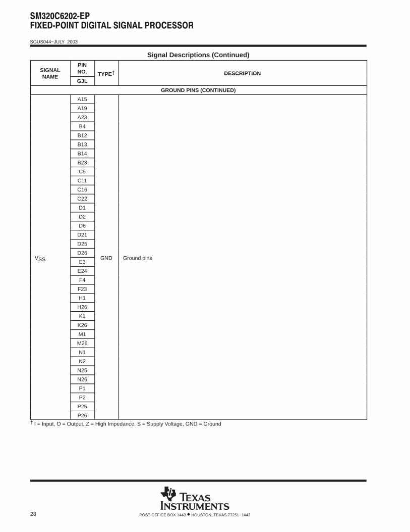
SGUS044−JULY 2003
32 POST OFFICE BOX 1443 • HOUSTON, TEXAS 77251−1443
device and development-support tool nomenclature (continued)
Table 14. SM320C6202 Device Part Numbers (P/Ns) and Ordering Information
DEVICE ORDERABLE P/N DEVICE SPEEDCVDD
(CORE VOLTAGE)DVDD
(I/O VOLTAGE)
OPERATING CASETEMPERATURE
RANGE
SM320C6202GJLA20EP 200 MHz/1600 MIPS 1.8 V 3.3 V −40C to105C
PREFIX
DEVICE SPEED RANGE
SM 320 C 6202 GJL 20
TMX= Experimental deviceTMP= Prototype deviceTMS= Qualified deviceSMJ = MIL-PRF-38535, QMLSM = Commercial processing
DEVICE FAMILY320 = TMS320 DSP family
TECHNOLOGY
PACKAGE TYPE †GFN = 256-pin plastic BGAGGP = 352-pin plastic BGAGJC = 352-pin plastic BGAGJL = 352-pin plastic BGAGLS = 384-pin plastic BGAGLW = 340-pin plastic BGAGNY = 384-pin plastic BGAGNZ = 352-pin plastic BGAGHK = 288-pin plastic MicroStar BGA
C = CMOS
DEVICE
† BGA = Ball Grid Array
TEMPERATURE RANGE (DEFAULT: 0 °C TO 90°C)
( )
Blank = 0°C to 90°C, commercial temperatureA = −40°C to 105°C, extended temperature
20 = 200 MHz
C6000 DSP:6201 6205 6415 6711C6202 6211 6416 67126202B 6211B 6701 6712C6203B 6411 6711 67136204 6414 6711B
EP
ENHANCED PLASTIC DESIGNATOR
Figure 4. TMS320C6000 DSP Platform Device Nomenclature (Including SM320C6202)
MicroStar BGA is a trademark of Texas Instruments.

SGUS044−JULY 2003
33POST OFFICE BOX 1443 • HOUSTON, TEXAS 77251−1443
documentation support
Extensive documentation supports all TMS320 DSP family devices from product announcement throughapplications development. The types of documentation available include: data sheets, such as this document,with design specifications; complete user’s reference guides for all devices and tools; technical briefs;development-support tools; on-line help; and hardware and software applications. The following is a brief,descriptive list of support documentation specific to the C6000 DSP devices:
The TMS320C6000 CPU and Instruction Set Reference Guide (literature number SPRU189) describes theC6000 CPU (DSP core) architecture, instruction set, pipeline, and associated interrupts.
The TMS320C6000 Peripherals Reference Guide (literature number SPRU190) describes the functionality ofthe peripherals available on the C6000 DSP platform of devices, such as the 64-/32-/16-bit external memoryinterfaces (EMIFs), 32-/16-bit host-port interfaces (HPIs), multichannel buffered serial ports (McBSPs), directmemory access (DMA), enhanced direct-memory-access (EDMA) controller, expansion bus (XBus), peripheralcomponent interconnect (PCI), clocking and phase-locked loop (PLL); and power-down modes. This guide alsoincludes information on internal data and program memories.
The How to Begin Development Today and Migrate Across the TMS320C6202/02B/03B/04 DSPs applicationreport (literature number SPRA603) describes the migration concerns and identifies the similarities anddifferences between the C6202, C6202B, C6203B, and C6204 C6000 DSP devices.
The TMS320C6202 Digital Signal Processor Silicon Errata (literature number SPRZ152) describes the knownexceptions to the functional specifications for particular silicon revisions of the TMS320C6202 device . Thereare currently no known silicon advisories on the TMS320C6202B device.
The Using IBIS Models for Timing Analysis application report (literature number SPRA839) describes how toproperly use IBIS models to attain accurate timing analysis for a given system.
The tools support documentation is electronically available within the Code Composer Studio IDE. For acomplete listing of the latest C6000 DSP documentation, visit the Texas Instruments web site on theWorldwide Web at http://www.ti.com uniform resource locator (URL).

SGUS044−JULY 2003
34 POST OFFICE BOX 1443 • HOUSTON, TEXAS 77251−1443
clock PLL All of the internal C6202 clocks are generated from a single source through the CLKIN pin. This source clockeither drives the PLL, which multiplies the source clock in frequency to generate the internal CPU clock, orbypasses the PLL to become the internal CPU clock.
To use the PLL to generate the CPU clock, the external PLL filter circuit must be properly designed. Figure 5,and Table 15 show the external PLL circuitry for either x1 (PLL bypass) or x4 PLL multiply modes. Figure 6shows the external PLL circuitry for a system with ONLY x1 (PLL bypass) mode.
To minimize the clock jitter, a single clean power supply should power both the C6202 device and the externalclock oscillator circuit. Noise coupling into PLLF directly impacts PLL clock jitter. The minimum CLKIN rise andfall times should also be observed. For the input clock timing requirements, see the Input and Output Clockselectricals section.
CLKMODE0CLKMODE1†
PLL
PLLV
CLKINLOOP FILTER
PLLCLK
PLLMULT
CLKIN
PLL
GC2
Internal to C6202
CPUCLOCK
C1R1
3.3V
10 F 0.1 F
PLL
F
EM
I Filt
er
C3 C4
1
0
CLKMODE2†
(For the PLL Optionsand CLKMODE pins setup,
see Table 15)
† CLKMODE1 and CLKMODE2 pins are not applicable (N/A) to the C6202 GJL package.
NOTES: A. Keep the lead length and the number of vias between pin PLLF, pin PLLG, R1, C1, and C2 to a minimum. In addition, place all PLLcomponents (R1, C1, C2, C3, C4, and EMI Filter) as close to the C6000 DSP device as possible. Best performance is achievedwith the PLL components on a single side of the board without jumpers, switches, or components other than the ones shown.
B. For reduced PLL jitter, maximize the spacing between switching signals and the PLL external components (R1, C1, C2, C3, C4,and the EMI Filter).
C. The 3.3-V supply for the EMI filter must be from the same 3.3-V power plane supplying the I/O voltage, DVDD.D. EMI filter manufacturer: TDK part number ACF451832-333, 223, 153, 103. Panasonic part number EXCCET103U.
Figure 5. External PLL Circuitry for Either PLL Multiply Modes or x1 (Bypass) Mode
PLL
PLLV
CLKIN
LOOP FILTER
PLLCLK
PLLMULT
CLKIN
PLL
G
Internal to C6202
CPUCLOCK
PLL
F
1
0
3.3V
CLKMODE0CLKMODE1†CLKMODE2†
† CLKMODE1 and CLKMODE2 pins are not applicable (N/A) to the C6202 GJL package.
NOTES: A. For a system with ONLY PLL x1 (bypass) mode, short the PLLF to PLLG.B. The 3.3-V supply for PLLV must be from the same 3.3-V power plane supplying the I/O voltage, DVDD.
Figure 6. External PLL Circuitry for x1 (Bypass) PLL Mode Only

SGUS044−JULY 2003
35POST OFFICE BOX 1443 • HOUSTON, TEXAS 77251−1443
clock PLL (continued)
Table 15. SM320C6202 GJL Package PLL Multiply and Bypass (x1) Options †
GJL PACKAGE 27 X 27 MM BGA
BIT (PIN NO.) CLKMODE0 (B15)DEVICES AND PLL CLOCK OPTIONS
BIT (PIN NO.) CLKMODE0 (B15)C6202 (GJL)§
Value0 Bypass (x1)
Value1 x4
† f(CPU Clock) = f(CLKIN) x (PLL mode)§ CLKMODE2 and CLKMODE1 pins are not available on the C6202 GJL package.
Table 16. SM320C6202 PLL Component Selection Table †
CLKMODECLKINRANGE(MHZ)
CPU CLOCKFREQUENCY(CLKOUT1)
RANGE (MHZ)
CLKOUT2RANGE(MHZ)
R1 [±1%] C1 [±10%] C2 [±10%]TYPICAL
LOCK TIME(ΜS)
x4 32.5−62.5 130−250 65−125 60.4 Ω 27 nF 560 pF 75† Under some operating conditions, the maximum PLL lock time may vary by as much as 150% from the specified typical value. For example, if
the typical lock time is specified as 100 µs, the maximum value may be as long as 250 µs.
power-supply sequencing
TI DSPs do not require specific power sequencing between the core supply and the I/O supply. However,systems should be designed to ensure that neither supply is powered up for extended periods of time(>1 second) if the other supply is below the proper operating voltage.
system-level design considerations
System-level design considerations, such as bus contention, may require supply sequencing to beimplemented. In this case, the core supply should be powered up at the same time as, or prior to (and powereddown after), the I/O buffers. This is to ensure that the I/O buffers receive valid inputs from the core before theoutput buffers are powered up, thus, preventing bus contention with other chips on the board.
power-supply design considerations
A dual-power supply with simultaneous sequencing can be used to eliminate the delay between core and I/Opower up. A Schottky diode can also be used to tie the core rail to the I/O rail (see Figure 7).
DVDD
CVDD
VSS
C6000DSP
SchottkyDiode
I/O Supply
Core Supply
GND
Figure 7. Schottky Diode Diagram

SGUS044−JULY 2003
36 POST OFFICE BOX 1443 • HOUSTON, TEXAS 77251−1443
Core and I/O supply voltage regulators should be located close to the DSP (or DSP array) to minimizeinductance and resistance in the power delivery path. Additionally, when designing for high-performanceapplications utilizing the C6000 platform of DSPs, the PC board should include separate power planes forcore, I/O, and ground, all bypassed with high-quality low-ESL/ESR capacitors.
On systems using C62x and C67x DSPs, the core may consume in excess of 2 A per DSP until the I/O supplypowers on. This extra current results from uninitialized logic within the DSP(s). A normal current state returnsonce the I/O power supply turns on and the CPU sees a clock pulse. Decreasing the amount of time betweenthe core supply power-up and the I/O supply power-up reduces the effects of the current draw. If the externalsupply to the DSP core cannot supply the excess current, the minimum core voltage may not be achieved untilafter normal current returns. This voltage starvation of the core supply during power up will not affect run-timeoperation. Voltage starvation can affect power supply systems that gate the I/O supply via the core supply,causing the I/O supply to never turn on. During the transition from excess to normal current, a voltage spike maybe seen on the core supply. Care must be taken when designing overvoltage protection circuitry on the coresupply to not restart the power sequence due to this spike. Otherwise, the supply may cycle indefinitely.
IEEE 1149.1 JTAG compatibility statement
For compatibility with IEEE 1149.1 JTAG programmers, the TRST pin may need to be externally pulled up viaa 1-kΩ resistor. For these C62x devices, this pin is internally pulled down, holding the JTAG port in reset bydefault. This is typically only a problem in systems where the DSP shares a scan chain with some other device.Some JTAG programmers for these other devices do not actively drive TRST high, leaving the scan chaininoperable while the C62x JTAG port is held in reset. TI emulators do drive TRST high, so the external pullupresistor is not needed in systems where TI emulators are the only devices that control JTAG scan chains onwhich the DSP(s) reside. If the system has other devices in the same scan chain as the DSP, and theprogrammer for these devices does not drive TRST high, then an external 1-kΩ pullup resistor is required.
With this external 1-kΩ pullup resistor installed, care must be taken to keep the DSP in a usable state underall circumstances. When TRST is pulled up, the JTAG driver must maintain the TMS signal high for 5 TCLKcycles, forcing the DSP(s) into the test logic reset (TLR) state. From the TLR state, the DSP’s data scan pathcan be put in bypass (scan all 1s into the IR) to scan the other devices. The TLR state also allows normaloperation of the DSP. If operation without anything driving the JTAG port is desired, the pullup resistor shouldbe jumpered so that it may be engaged for programming the other devices and disconneted for running withouta JTAG programmer or emulator.

SGUS044−JULY 2003
37POST OFFICE BOX 1443 • HOUSTON, TEXAS 77251−1443
absolute maximum ratings over operating case temperature ranges (unless otherwise noted) † Supply voltage range, CVDD (see Note 1) −0.3 V to 2.3 V. . . . . . . . . . . . . . . . . . . . . . . . . . . . . . . . . . . . . . . . . . . . Supply voltage range, DVDD (see Note 1) −0.3 V to 4 V. . . . . . . . . . . . . . . . . . . . . . . . . . . . . . . . . . . . . . . . . . . . . Input voltage range −0.3 V to 4 V. . . . . . . . . . . . . . . . . . . . . . . . . . . . . . . . . . . . . . . . . . . . . . . . . . . . . . . . . . . . . . . . . Output voltage range −0.3 V to 4 V. . . . . . . . . . . . . . . . . . . . . . . . . . . . . . . . . . . . . . . . . . . . . . . . . . . . . . . . . . . . . . . Operating case temperature ranges, TC:(A version) −40C to105C. . . . . . . . . . . . . . . . . . . . . . . . . . . . . . . Storage temperature range, Tstg −65C to 150C. . . . . . . . . . . . . . . . . . . . . . . . . . . . . . . . . . . . . . . . . . . . . . . Temperature cycle range, (1000-cycle performance) −40C to 125C. . . . . . . . . . . . . . . . . . . . . . . . . . . . . . .
† Stresses beyond those listed under “absolute maximum ratings” may cause permanent damage to the device. These are stress ratings only, andfunctional operation of the device at these or any other conditions beyond those indicated under “recommended operating conditions” is notimplied. Exposure to absolute-maximum-rated conditions for extended periods may affect device reliability.
NOTE 1: All voltage values are with respect to VSS.
recommended operating conditions
MIN NOM MAX UNIT
CVDD Supply voltage, Core 1.71 1.8 1.89 V
DVDD Supply voltage, I/O 3.14 3.3 3.46 V
VSS Supply ground 0 0 0 V
VIH High-level input voltage 2 V
VIL Low-level input voltage 0.8 V
IOH High-level output current −8 mA
IOL Low-level output current 8 mA
TC Operating case temperature A version −40 105 C
electrical characteristics over recommended ranges of supply voltage and operating casetemperature (unless otherwise noted)
PARAMETER TEST CONDITIONS MIN TYP MAX UNIT
VOH High-level output voltage DVDD = MIN, IOH = MAX 2.4 V
VOL Low-level output voltage DVDD = MIN, IOL = MAX 0.6 V
II Input current‡ VI = VSS to DVDD ±10 uA
IOZ Off-state output current VO = DVDD or 0 V ±10 uA
IDD2VSupply current, CPU + CPU memoryaccess§ CVDD = NOM, CPU clock = 200 MHz 520 mA
IDD2V Supply current, peripherals§ CVDD = NOM, CPU clock = 200 MHz 390 mA
IDD3V Supply current, I/O pins§ DVDD = NOM, CPU clock = 200 MHz 70 mA
Ci Input capacitance 10 pF
Co Output capacitance 10 pF
‡ TMS and TDI are not included due to internal pullups. TRST is not included due to internal pulldown.§ Measured with average activity (50% high / 50% low power). For more details on CPU, peripheral, and I/O activity, see the TMS320C6000 Power
Consumption Summary application report (literature number SPRA486).

SGUS044−JULY 2003
38 POST OFFICE BOX 1443 • HOUSTON, TEXAS 77251−1443
PARAMETER MEASUREMENT INFORMATION
Tester PinElectronics
Vcomm
IOL
CT†
IOH
OutputUnderTest
50 Ω
Where: IOL = 2 mAIOH = 2 mAVcomm = 1.5 VCT = 15-pF typical load-circuit capacitance
† Typical distributed load circuit capacitance
Figure 8. Test Load Circuit for AC Timing Measurements
signal transition levels
All input and output timing parameters are referenced to 1.5 V for both “0” and “1” logic levels.
Vref = 1.5 V
Figure 9. Input and Output Voltage Reference Levels for ac Timing Measurements
All rise and fall transition timing parameters are referenced to VIL MAX and VIH MIN for input clocks, andVOL MAX and VOH MIN for output clocks.
Vref = VIL MAX (or V OL MAX)
Vref = VIH MIN (or VOH MIN)
Figure 10. Rise and Fall Transition Time Voltage Reference Levels

SGUS044−JULY 2003
39POST OFFICE BOX 1443 • HOUSTON, TEXAS 77251−1443
PARAMETER MEASUREMENT INFORMATION (CONTINUED)
timing parameters and board routing analysis
The timing parameter values specified in this data sheet do not include delays by board routings. As a goodboard design practice, such delays must always be taken into account. Timing values may be adjusted byincreasing/decreasing such delays. TI recommends utilizing the available I/O buffer information specification(IBIS) models to analyze the timing characteristics correctly. To properly use IBIS models to attain accuratetiming analysis for a given system, see the Using IBIS Models for Timing Analysis application report (literaturenumber SPRA839). If needed, external logic hardware such as buffers may be used to compensate any timingdifferences.
For inputs, timing is most impacted by the round-trip propagation delay from the DSP to the external device andfrom the external device to the DSP. This round-trip delay tends to negatively impact the input setup time margin,but also tends to improve the input hold time margins (see Table 17 and Figure 11).
Figure 11 represents a general transfer between the DSP and an external device. The figure also representsboard route delays and how they are perceived by the DSP and the external device.
Table 17. Board-Level TImings Example (see Figure 11)
NO. DESCRIPTION
1 Clock route delay
2 Minimum DSP hold time
3 Minimum DSP setup time
4 External device hold time requirement
5 External device setup time requirement
6 Control signal route delay
7 External device hold time
8 External device access time
9 DSP hold time requirement
10 DSP setup time requirement
11 Data route delay
1
23
45
6
78
1011
CLKOUT2(Output from DSP)
CLKOUT2(Input to External Device)
Control Signals †
(Output from DSP)
Control Signals(Input to External Device)
Data Signals ‡
(Output from External Device)
Data Signals ‡
(Input to DSP)
9
† Control signals include data for Writes.‡ Data signals are generated during Reads from an external device.
Figure 11. Board-Level Input/Output Timings

SGUS044−JULY 2003
40 POST OFFICE BOX 1443 • HOUSTON, TEXAS 77251−1443
INPUT AND OUTPUT CLOCKS
timing requirements for CLKIN (PLL used) †‡§ (see Figure 12)
NO.C6202-20
UNITNO.MIN MAX
UNIT
1 tc(CLKIN) Cycle time, CLKIN 5 * M ns
2 tw(CLKINH) Pulse duration, CLKIN high 0.4C ns
3 tw(CLKINL) Pulse duration, CLKIN low 0.4C ns
4 tt(CLKIN) Transition time, CLKIN 5 ns
† The reference points for the rise and fall transitions are measured at VIL MAX and VIH MIN.‡ M = the PLL multiplier factor (x4) for C6202 GJL only. For more details, see the Clock PLL section of this data sheet.§ C = CLKIN cycle time in ns. For example, when CLKIN frequency is 50 MHz, use C = 20 ns.
timing requirements for CLKIN [PLL bypassed (x1)] †¶ (see Figure 12)
NO.C6202-20
UNITNO.MIN MAX
UNIT
1 tc(CLKIN) Cycle time, CLKIN 5 ns
2 tw(CLKINH) Pulse duration, CLKIN high 0.45C ns
3 tw(CLKINL) Pulse duration, CLKIN low 0.45C ns
4 tt(CLKIN) Transition time, CLKIN 0.6 ns
† The reference points for the rise and fall transitions are measured at VIL MAX and VIH MIN.¶ C = CLKIN cycle time in ns. For example, when CLKIN frequency is 50 MHz, use C = 20 ns. The maximum CLKIN cycle time is PLL bypass mode
(x1) is 200 MHz.
CLKIN
1
2
3
4
4
Figure 12. CLKIN Timings

SGUS044−JULY 2003
41POST OFFICE BOX 1443 • HOUSTON, TEXAS 77251−1443
INPUT AND OUTPUT CLOCKS (CONTINUED)
timing requirements for XCLKIN † (see Figure 13)
NO.C6202-20
UNITNO.MIN MAX
UNIT
1 tc(XCLKIN) Cycle time, XCLKIN 4P ns
2 tw(XCLKINH) Pulse duration, XCLKIN high 1.8P ns
3 tw(XCLKINL) Pulse duration, XCLKIN low 1.8P ns
† P = 1/CPU clock frequency in nanoseconds (ns).
XCLKIN
1
2
3
Figure 13. XCLKIN Timings
switching characteristics over recommended operating conditions for CLKOUT2 ठ(see Figure 14)
NO. PARAMETERC6202-20
UNITNO. PARAMETERMIN MAX
UNIT
1 tc(CKO2) Cycle time, CLKOUT2 2P−0.7 2P + 0.7 ns
2 tw(CKO2H) Pulse duration, CLKOUT2 high P−0.7 P + 0.7 ns
3 tw(CKO2L) Pulse duration, CLKOUT2 low P−0.7 P + 0.7 ns
‡ P = 1/CPU clock frequency in ns.§ The reference points for the rise and fall transitions are measured at VOL MAX and VOH MIN.
CLKOUT2
1
3
2
Figure 14. CLKOUT2 Timings

SGUS044−JULY 2003
42 POST OFFICE BOX 1443 • HOUSTON, TEXAS 77251−1443
INPUT AND OUTPUT CLOCKS (CONTINUED)
switching characteristics over recommended operating conditions for XFCLK †‡ (see Figure 15)
NO. PARAMETERC6202-20
UNITNO. PARAMETERMIN MAX
UNIT
1 tc(XFCK) Cycle time, XFCLK D * P−0.7 D * P + 0.7 ns
2 tw(XFCKH) Pulse duration, XFCLK high (D/2) * P−0.7 (D/2) * P + 0.7 ns
3 tw(XFCKL) Pulse duration, XFCLK low (D/2) * P−0.7 (D/2) * P + 0.7 ns
† P = 1/CPU clock frequency in ns.‡ D = 8, 6, 4, or 2; FIFO clock divide ratio, user-programmable
XFCLK
1
2
3
Figure 15. XFCLK Timings
ASYNCHRONOUS MEMORY TIMING
timing requirements for asynchronous memory cycles †‡§¶ (see Figure 16−Figure 19)
NO.C6202-20
UNITNO.MIN MAX
UNIT
3 tsu(EDV-AREH) Setup time, EDx valid before ARE high 1 ns
4 th(AREH-EDV) Hold time, EDx valid after ARE high 3.5 ns
6 tsu(ARDYH-AREL) Setup time, ARDY high before ARE low −[(RST−3) * P−6] ns
7 th(AREL-ARDYH) Hold time, ARDY high after ARE low (RST−3) * P + 2 ns
9 tsu(ARDYL-AREL) Setup time, ARDY low before ARE low −[(RST−3) * P−6] ns
10 th(AREL-ARDYL) Hold time, ARDY low after ARE low (RST−3) * P + 2 ns
11 tw(ARDYH) Pulse width, ARDY high 2P ns
15 tsu(ARDYH-AWEL) Setup time, ARDY high before AWE low −[(WST−3) * P−6] ns
16 th(AWEL-ARDYH) Hold time, ARDY high after AWE low (WST−3) * P + 2 ns
18 tsu(ARDYL-AWEL) Setup time, ARDY low before AWE low −[(WST−3) * P−6] ns
19 th(AWEL-ARDYL) Hold time, ARDY low after AWE low (WST−3) * P + 2 ns
† To ensure data setup time, simply program the strobe width wide enough. ARDY is internally synchronized. If ARDY does meet setup or holdtime, it may be recognized in the current cycle or the next cycle. Thus, ARDY can be an asynchronous input.
‡ RS = Read Setup, RST = Read Strobe, RH = Read Hold, WS = Write Setup, WST = Write Strobe, WH = Write Hold. These parameters areprogrammed via the EMIF CE space control registers.
§ P = 1/CPU clock frequency in ns.¶ The sum of RS and RST (or WS and WST) must be a minimum of 4 in order to use ARDY input to extend strobe width.

SGUS044−JULY 2003
43POST OFFICE BOX 1443 • HOUSTON, TEXAS 77251−1443
ASYNCHRONOUS MEMORY TIMING (CONTINUED)
switching characteristics over recommended operating conditions for asynchronous memorycycles †‡§¶ (see Figure 16−Figure 19)
NO. PARAMETERC6202-20
UNITNO. PARAMETERMIN TYP MAX
UNIT
1 tosu(SELV-AREL) Output setup time, select signals valid to ARE low RS * P−2 ns
2 toh(AREH-SELIV) Output hold time, ARE high to select signals invalid RH * P−2 ns
5 tw(AREL) Pulse width, ARE low RST * P ns
8 td(ARDYH-AREH) Delay time, ARDY high to ARE high 3P 4P + 5 ns
12 tosu(SELV-AWEL) Output setup time, select signals valid to AWE low WS * P−3 ns
13 toh(AWEH-SELIV) Output hold time, AWE high to select signals invalid WH * P−2 ns
14 tw(AWEL) Pulse width, AWE low WST * P ns
17 td(ARDYH-AWEH) Delay time, ARDY high to AWE high 3P 4P + 5 ns
† RS = Read Setup, RST = Read Strobe, RH = Read Hold, WS = Write Setup, WST = Write Strobe, WH = Write Hold. These parameters areprogrammed via the EMIF CE space control registers.
‡ P = 1/CPU clock frequency in ns.§ The sum of RS and RST (or WS and WST) must be a minimum of 4 in order to use ARDY input to extend strobe width.¶ Select signals include: CEx, BE[3:0], EA[21:2], AOE; and for writes, include ED[31:0], with the exception that CEx can stay active for an additional
7P ns following the end of the cycle.

SGUS044−JULY 2003
44 POST OFFICE BOX 1443 • HOUSTON, TEXAS 77251−1443
ASYNCHRONOUS MEMORY TIMING (CONTINUED)
Setup = 2 Strobe = 3 Hold = 2
5
21
43
21
21
76
CLKOUT1
CEx
BE[3:0]
ED[31:0]
AOE
ARE
AWE
ARDY
21EA[21:2]
Figure 16. Asynchronous Memory Read Timing (ARDY Not Used)
Setup = 2 Strobe = 3 Not Ready Hold = 2
8
21
43
21
21
21
11
109
CLKOUT1
CEx
BE[3:0]
ED[31:0]
AOE
ARE
AWE
ARDY
EA[21:2]
Figure 17. Asynchronous Memory Read Timing (ARDY Used)

SGUS044−JULY 2003
45POST OFFICE BOX 1443 • HOUSTON, TEXAS 77251−1443
ASYNCHRONOUS MEMORY TIMING (CONTINUED)
Setup = 2 Strobe = 3 Hold = 2
14
1312
1312
1312
1312
1615
CEx
BE[3:0]
ED[31:0]
AOE
ARE
AWE
ARDY
EA[21:2]
CLKOUT1
Figure 18. Asynchronous Memory Write Timing (ARDY Not Used)
Setup = 2 Strobe = 3 Not Ready Hold = 2
17
1312
1312
1312
1312
11
1918
CEx
BE[3:0]
EA[21:2]
ED[31:0]
AOE
ARE
AWE
ARDY
CLKOUT1
Figure 19. Asynchronous Memory Write Timing (ARDY Used)

SGUS044−JULY 2003
46 POST OFFICE BOX 1443 • HOUSTON, TEXAS 77251−1443
SYNCHRONOUS-BURST MEMORY TIMING
timing requirements for synchronous-burst SRAM cycles for C6202 devices (see Figure 20)
NO.C6202-20
UNITNO.MIN MAX
UNIT
7 tsu(EDV-CKO2H) Setup time, read EDx valid before CLKOUT2 high 2.5 ns
8 th(CKO2H-EDV) Hold time, read EDx valid after CLKOUT2 high 2.0 ns
switching characteristics over recommended operating conditions for synchronous-burst SRAMcycles for C6202 devices †‡ (see Figure 20 and Figure 21)
NO. PARAMETERC6202-20
UNITNO. PARAMETERMIN MAX
UNIT
1 tosu(CEV-CKO2H) Output setup time, CEx valid before CLKOUT2 high P−0.8 ns
2 toh(CKO2H-CEV) Output hold time, CEx valid after CLKOUT2 high P−4 ns
3 tosu(BEV-CKO2H) Output setup time, BEx valid before CLKOUT2 high P−0.8 ns
4 toh(CKO2H-BEIV) Output hold time, BEx invalid after CLKOUT2 high P−4 ns
5 tosu(EAV-CKO2H) Output setup time, EAx valid before CLKOUT2 high P−0.8 ns
6 toh(CKO2H-EAIV) Output hold time, EAx invalid after CLKOUT2 high P−4 ns
9 tosu(ADSV-CKO2H) Output setup time, SDCAS/SSADS valid before CLKOUT2 high P−0.8 ns
10 toh(CKO2H-ADSV) Output hold time, SDCAS/SSADS valid after CLKOUT2 high P−4 ns
11 tosu(OEV-CKO2H) Output setup time, SDRAS/SSOE valid before CLKOUT2 high P−0.8 ns
12 toh(CKO2H-OEV) Output hold time, SDRAS/SSOE valid after CLKOUT2 high P−4 ns
13 tosu(EDV-CKO2H) Output setup time, EDx valid before CLKOUT2 high§ P−1.2 ns
14 toh(CKO2H-EDIV) Output hold time, EDx invalid after CLKOUT2 high P−4 ns
15 tosu(WEV-CKO2H) Output setup time, SDWE/SSWE valid before CLKOUT2 high P−0.8 ns
16 toh(CKO2H-WEV) Output hold time, SDWE/SSWE valid after CLKOUT2 high P−4 ns
† P = 1/CPU clock frequency in ns.‡ SDCAS/SSADS, SDRAS/SSOE, and SDWE/SSWE operate as SSADS, SSOE, and SSWE, respectively, during SBSRAM accesses.§ For the first write in a series of one or more consecutive adjacent writes, the write data is generated one CLKOUT2 cycle early to accommodate
the ED enable time.

SGUS044−JULY 2003
47POST OFFICE BOX 1443 • HOUSTON, TEXAS 77251−1443
SYNCHRONOUS-BURST MEMORY TIMING (CONTINUED)
CLKOUT2
CEx
BE[3:0]
EA[21:2]
ED[31:0]
SDCAS/SSADS†
SDRAS/SSOE†
SDWE/SSWE†
BE1 BE2 BE3 BE4
A1 A2 A3 A4
Q1 Q2 Q3 Q4
1211
109
65
43
21
87
† SDCAS/SSADS, SDRAS/SSOE, and SDWE/SSWE operate as SSADS, SSOE, and SSWE, respectively, during SBSRAM accesses.
Figure 20. SBSRAM Read Timing
CLKOUT2
CEx
BE[3:0]
EA[21:2]
ED[31:0]
SDRAS/SSOE†
SDWE/SSWE†
SDCAS/SSADS†
BE1 BE2 BE3 BE4
A1 A2 A3 A4
Q1 Q2 Q3 Q4
1615
109
1413
65
43
21
† SDCAS/SSADS, SDRAS/SSOE, and SDWE/SSWE operate as SSADS, SSOE, and SSWE, respectively, during SBSRAM accesses.
Figure 21. SBSRAM Write Timing

SGUS044−JULY 2003
48 POST OFFICE BOX 1443 • HOUSTON, TEXAS 77251−1443
SYNCHRONOUS DRAM TIMING
timing requirements for synchronous DRAM cycles for C6202 devices (see Figure 22)
NO.C6202-20
UNITNO.MIN MAX
UNIT
7 tsu(EDV-CKO2H) Setup time, read EDx valid before CLKOUT2 high 1.2 ns
8 th(CKO2H-EDV) Hold time, read EDx valid after CLKOUT2 high 3 ns
switching characteristics over recommended operating conditions for synchronous DRAM cyclesfor C6202 devices †‡ (see Figure 22−Figure 27)
NO. PARAMETERC6202-20
UNITNO. PARAMETERMIN MAX
UNIT
1 tosu(CEV-CKO2H) Output setup time, CEx valid before CLKOUT2 high P−1 ns
2 toh(CKO2H-CEV) Output hold time, CEx valid after CLKOUT2 high P−3.5 ns
3 tosu(BEV-CKO2H) Output setup time, BEx valid before CLKOUT2 high P−1 ns
4 toh(CKO2H-BEIV) Output hold time, BEx invalid after CLKOUT2 high P−3.5 ns
5 tosu(EAV-CKO2H) Output setup time, EAx valid before CLKOUT2 high P−1 ns
6 toh(CKO2H-EAIV) Output hold time, EAx invalid after CLKOUT2 high P−3.5 ns
9 tosu(CASV-CKO2H) Output setup time, SDCAS/SSADS valid before CLKOUT2 high P−1 ns
10 toh(CKO2H-CASV) Output hold time, SDCAS/SSADS valid after CLKOUT2 high P−3.5 ns
11 tosu(EDV-CKO2H) Output setup time, EDx valid before CLKOUT2 high§ P−1 ns
12 toh(CKO2H-EDIV) Output hold time, EDx invalid after CLKOUT2 high P−3.5 ns
13 tosu(WEV-CKO2H) Output setup time, SDWE/SSWE valid before CLKOUT2 high P−1 ns
14 toh(CKO2H-WEV) Output hold time, SDWE/SSWE valid after CLKOUT2 high P−3.5 ns
15 tosu(SDA10V-CKO2H) Output setup time, SDA10 valid before CLKOUT2 high P−1 ns
16 toh(CKO2H-SDA10IV) Output hold time, SDA10 invalid after CLKOUT2 high P−3.5 ns
17 tosu(RASV-CKO2H) Output setup time, SDRAS/SSOE valid before CLKOUT2 high P−1 ns
18 toh(CKO2H-RASV) Output hold time, SDRAS/SSOE valid after CLKOUT2 high P−3.5 ns
† P = 1/CPU clock frequency in ns.‡ SDCAS/SSADS, SDRAS/SSOE, and SDWE/SSWE operate as SDCAS, SDRAS, and SDWE, respectively, during SDRAM accesses.§ For the first write in a series of one or more consecutive adjacent writes, the write data is generated one CLKOUT2 cycle early to accommodate
the ED enable time.

SGUS044−JULY 2003
49POST OFFICE BOX 1443 • HOUSTON, TEXAS 77251−1443
SYNCHRONOUS DRAM TIMING (CONTINUED)
CLKOUT2
CEx
BE[3:0]
EA[15:2]
ED[31:0]
SDA10
SDRAS/SSOE†
SDCAS/SSADS†
SDWE/SSWE†
BE1 BE2 BE3
CA1 CA2 CA3
D1 D2 D3
109
1615
65
43
21
87
READREADREAD
† SDCAS/SSADS, SDRAS/SSOE, and SDWE/SSWE operate as SDCAS, SDRAS, and SDWE, respectively, during SDRAM accesses.
Figure 22. Three SDRAM READ Commands
CLKOUT2
CEx
BE[3:0]
EA[15:2]
ED[31:0]
SDA10
SDRAS/SSOE†
SDCAS/SSADS†
SDWE/SSWE†
BE1 BE2 BE3
CA1 CA2 CA3
D1 D2 D3
1413
109
1615
1211
65
43
21
WRITEWRITEWRITE
† SDCAS/SSADS, SDRAS/SSOE, and SDWE/SSWE operate as SDCAS, SDRAS, and SDWE, respectively, during SDRAM accesses.
Figure 23. Three SDRAM WRT Commands

SGUS044−JULY 2003
50 POST OFFICE BOX 1443 • HOUSTON, TEXAS 77251−1443
SYNCHRONOUS DRAM TIMING (CONTINUED)
CLKOUT2
CEx
BE[3:0]
EA[15:2]
ED[31:0]
SDA10
SDRAS/SSOE†
SDCAS/SSADS†
SDWE/SSWE†
Bank Activate/Row Address
Row Address
1817
15
5
21
ACTV
† SDCAS/SSADS, SDRAS/SSOE, and SDWE/SSWE operate as SDCAS, SDRAS, and SDWE, respectively, during SDRAM accesses.
Figure 24. SDRAM ACTV Command
CLKOUT2
CEx
BE[3:0]
EA[15:2]
ED[31:0]
SDA10
SDRAS/SSOE†
SDCAS/SSADS†
SDWE/SSWE†14
18
16
2
15
1
17
13
DCAB
† SDCAS/SSADS, SDRAS/SSOE, and SDWE/SSWE operate as SDCAS, SDRAS, and SDWE, respectively, during SDRAM accesses.
Figure 25. SDRAM DCAB Command

SGUS044−JULY 2003
51POST OFFICE BOX 1443 • HOUSTON, TEXAS 77251−1443
SYNCHRONOUS DRAM TIMING (CONTINUED)
CLKOUT2
CEx
BE[3:0]
EA[15:2]
ED[31:0]
SDA10
SDRAS/SSOE†
SDCAS/SSADS†
SDWE/SSWE†
109
1817
21
REFR
† SDCAS/SSADS, SDRAS/SSOE, and SDWE/SSWE operate as SDCAS, SDRAS, and SDWE, respectively, during SDRAM accesses.
Figure 26. SDRAM REFR Command
CLKOUT2
CEx
BE[3:0]
EA[15:2]
ED[31:0]
SDA10
SDRAS/SSOE†
SDCAS/SSADS†
SDWE/SSWE†
MRS Value
14
10
18
6
21
5
17
9
13
MRS
† SDCAS/SSADS, SDRAS/SSOE, and SDWE/SSWE operate as SDCAS, SDRAS, and SDWE, respectively, during SDRAM accesses.
Figure 27. SDRAM MRS Command

SGUS044−JULY 2003
52 POST OFFICE BOX 1443 • HOUSTON, TEXAS 77251−1443
HOLD/HOLDA TIMING
timing requirements for the HOLD /HOLDA cycles † (see Figure 28)
NO.C6202-20
UNITNO.MIN MAX
UNIT
3 toh(HOLDAL-HOLDL) Output hold time, HOLD low after HOLDA low P ns
† P = 1/CPU clock frequency in ns.
switching characteristics over recommended operating conditions for the HOLD /HOLDA cycles †‡
(see Figure 28)
NO. PARAMETERC6202-20
UNITNO. PARAMETERMIN MAX
UNIT
1 td(HOLDL-EMHZ) Delay time, HOLD low to EMIF Bus high impedance 3P § ns
2 td(EMHZ-HOLDAL) Delay time, EMIF Bus high impedance to HOLDA low 0 2P ns
4 td(HOLDH-EMLZ) Delay time, HOLD high to EMIF Bus low impedance 3P 7P ns
5 td(EMLZ-HOLDAH) Delay time, EMIF Bus low impedance to HOLDA high 0 2P ns
† P = 1/CPU clock frequency in ns.‡ EMIF Bus consists of CE[3:0], BE[3:0], ED[31:0], EA[21:2], ARE, AOE, AWE, SDCAS/SSADS, SDRAS/SSOE, SDWE/SSWE, and SDA10.§ All pending EMIF transactions are allowed to complete before HOLDA is asserted. The worst case for this is an asynchronous read or write with
external ARDY used or a minimum of eight consecutive SDRAM reads or writes when RBTR8 = 1. If no bus transactions are occurring, then theminimum delay time can be achieved. Also, bus hold can be indefinitely delayed by setting NOHOLD = 1.
HOLD
HOLDA
EMIF Bus †
DSP Owns BusExternal Requestor
Owns Bus DSP Owns Bus
C6202 C62021
3
2 5
4
† EMIF Bus consists of CE[3:0], BE[3:0], ED[31:0], EA[21:2], ARE, AOE, AWE, SDCAS/SSADS, SDRAS/SSOE, SDWE/SSWE, and SDA10.
Figure 28. HOLD /HOLDA Timing

SGUS044−JULY 2003
53POST OFFICE BOX 1443 • HOUSTON, TEXAS 77251−1443
RESET TIMING
timing requirements for reset † (see Figure 29)
NO.C6202-20
UNITNO.MIN MAX
UNIT
1 tw(RST)Width of the RESET pulse (PLL stable)‡ 10P ns
1 tw(RST) Width of the RESET pulse (PLL needs to sync up)§ 250 µs
10 tsu(XD) Setup time, XD configuration bits valid before RESET high¶ 5P ns
11 th(XD) Hold time, XD configuration bits valid after RESET high¶ 5P ns
† P = 1/CPU clock frequency in ns.‡ This parameter applies to CLKMODE x1 when CLKIN is stable, and applies to CLKMODE x4 only when CLKIN and PLL are stable for C6202.§ This parameter applies to CLKMODE x4 only (it does not apply to CLKMODE x1) for C6202. The RESET signal is not connected internally to
the clock PLL circuit. The PLL, however, may need up to 250 µs to stabilize following device power up or after PLL configuration has beenchanged. During that time, RESET must be asserted to ensure proper device operation. See the Clock PLL section for PLL lock times.
¶ XD[31:0] are the boot configuration pins during device reset.
switching characteristics over recommended operating conditions during reset †# (see Figure 29)
NO. PARAMETERC6202-20
UNITNO. PARAMETERMIN MAX
UNIT
2 td(RSTL-CKO2IV) Delay time, RESET low to CLKOUT2 invalid P ns
3 td(RSTH-CKO2V) Delay time, RESET high to CLKOUT2 valid 4P ns
4 td(RSTL-HIGHIV) Delay time, RESET low to high group invalid P ns
5 td(RSTH-HIGHV) Delay time, RESET high to high group valid 4P ns
6 td(RSTL-LOWIV) Delay time, RESET low to low group invalid P ns
7 td(RSTH-LOWV) Delay time, RESET high to low group valid 4P ns
8 td(RSTL-ZHZ) Delay time, RESET low to Z group high impedance P ns
9 td(RSTH-ZV) Delay time, RESET high to Z group valid 4P ns
† P = 1/CPU clock frequency in ns.# High group consists of: XFCLK, HOLDA
Low group consists of: IACK, INUM[3:0], DMAC[3:0], PD, TOUT0, and TOUT1Z group consists of: EA[21:2], ED[31:0], CE[3:0], BE[3:0], ARE, AWE, AOE, SDCAS/SSADS, SDRAS/SSOE, SDWE/SSWE,
SDA10, CLKX0, CLKX1, CLKX2, FSX0, FSX1, FSX2, DX0, DX1, DX2, CLKR0, CLKR1, CLKR2, FSR0, FSR1,FSR2, XCE[3:0], XBE[3:0]/XA[5:2], XOE, XRE, XWE/XWAIT, XAS, XW/R, XRDY, XBLAST, XHOLD,and XHOLDA

SGUS044−JULY 2003
54 POST OFFICE BOX 1443 • HOUSTON, TEXAS 77251−1443
RESET TIMING (CONTINUED)
CLKOUT1
98
76
54
32
1110
RESET
CLKOUT2
HIGH GROUP†
LOW GROUP†
Z GROUP†
XD[31:0] ‡
1
Boot Configuration
† High group consists of: XFCLK, HOLDALow group consists of: IACK, INUM[3:0], DMAC[3:0], PD, TOUT0, and TOUT1.Z group consists of: EA[21:2], ED[31:0], CE[3:0], BE[3:0], ARE, AWE, AOE, SDCAS/SSADS, SDRAS/SSOE, SDWE/SSWE,
SDA10, CLKX0, CLKX1, CLKX2, FSX0, FSX1, FSX2, DX0, DX1, DX2, CLKR0, CLKR1, CLKR2, FSR0, FSR1,FSR2, XCE[3:0], XBE[3:0]/XA[5:2], XOE, XRE, XWE/XWAIT, XAS, XW/R, XRDY, XBLAST, XHOLD,and XHOLDA.
‡ XD[31:0] are the boot configuration pins during device reset.
Figure 29. Reset Timing

SGUS044−JULY 2003
55POST OFFICE BOX 1443 • HOUSTON, TEXAS 77251−1443
EXTERNAL INTERRUPT TIMING
timing requirements for interrupt response cycles † (see Figure 30)
NO.C6202-20
UNITNO.MIN MAX
UNIT
2 tw(ILOW) Width of the interrupt pulse low 2P ns
3 tw(IHIGH) Width of the interrupt pulse high 2P ns
† P = 1/CPU clock frequency in ns.
switching characteristics over recommended operating conditions during interrupt responsecycles † (see Figure 30)
NO. PARAMETERC6202-20
UNITNO. PARAMETERMIN MAX
UNIT
1 tR(EINTH−IACKH) Response time, EXT_INTx high to IACK high 9P ns
4 td(CKO2L-IACKV) Delay time, CLKOUT2 low to IACK valid 1 10 ns
5 td(CKO2L-INUMV) Delay time, CLKOUT2 low to INUMx valid 0 10 ns
6 td(CKO2L-INUMIV) Delay time, CLKOUT2 low to INUMx invalid 0 10 ns
† P = 1/CPU clock frequency in ns.
Interrupt Number
65
44
32
CLKOUT2
EXT_INTx, NMI
1
Intr Flag
IACK
INUMx
Figure 30. Interrupt Timing

SGUS044 − JULY 2003
56 POST OFFICE BOX 1443 • HOUSTON, TEXAS 77251−1443
EXPANSION BUS SYNCHRONOUS FIFO TIMING
timing requirements for synchronous FIFO interface (see Figure 31, Figure 32, and Figure 33)
NO.C6202-20
UNITNO.MIN MAX
UNIT
5 tsu(XDV-XFCKH) Setup time, read XDx valid before XFCLK high 3 ns
6 th(XFCKH-XDV) Hold time, read XDx valid after XFCLK high 2.5 ns
switching characteristics over recommended operating conditions for synchronous FIFOinterface (see Figure 31, Figure 32, and Figure 33)
NO. PARAMETERC6202-20
UNITNO. PARAMETERMIN MAX
UNIT
1 td(XFCKH-XCEV) Delay time, XFCLK high to XCEx valid 1.5 5.2 ns
2 td(XFCKH-XAV) Delay time, XFCLK high to XBE[3:0]/XA[5:2] valid† 1.5 5.2 ns
3 td(XFCKH-XOEV) Delay time, XFCLK high to XOE valid 1.5 5.2 ns
4 td(XFCKH-XREV) Delay time, XFCLK high to XRE valid 1.5 5.2 ns
7 td(XFCKH-XWEV) Delay time, XFCLK high to XWE/XWAIT‡ valid 1.5 5.2 ns
8 td(XFCKH-XDV) Delay time, XFCLK high to XDx valid 5.2 ns
9 td(XFCKH-XDIV) Delay time, XFCLK high to XDx invalid 1.5 ns
† XBE[3:0]/XA[5:2] operate as address signals XA[5:2] during synchronous FIFO accesses.‡ XWE/XWAIT operates as the write-enable signal XWE during synchronous FIFO accesses.
XA1 XA2 XA3 XA4
D1 D2 D3 D4
65
44
33
22
11
XFCLK
XCE3†
XBE[3:0] /XA[5:2] ‡
XOE
XRE
XWE/XWAIT§
XD[31:0]
† FIFO read (glueless) mode only available in XCE3.‡ XBE[3:0]/XA[5:2] operate as address signals XA[5:2] during synchronous FIFO accesses.§ XWE/XWAIT operates as the write-enable signal XWE during synchronous FIFO accesses.
Figure 31. FIFO Read Timing (Glueless Read Mode)

SGUS044 − JULY 2003
57POST OFFICE BOX 1443 • HOUSTON, TEXAS 77251−1443
EXPANSION BUS SYNCHRONOUS FIFO TIMING (CONTINUED)
XA1 XA2 XA3 XA4
D1 D2 D3 D4
65
44
33
22
11
XFCLK
XCEx
XBE[3:0] /XA[5:2] †
XOE
XRE
XWE/XWAIT‡
XD[31:0]
† XBE[3:0]/XA[5:2] operate as address signals XA[5:2] during synchronous FIFO accesses.‡ XWE/XWAIT operates as the write-enable signal XWE during synchronous FIFO accesses.
Figure 32. FIFO Read Timing
XA1 XA2 XA3 XA4
D1 D2 D3 D4
98
77
22
11
XFCLK
XCEx
XBE[3:0] /XA[5:2] †
XOE
XRE
XD[31:0]
XWE/XWAIT‡
† XBE[3:0]/XA[5:2] operate as address signals XA[5:2] during synchronous FIFO accesses.‡ XWE/XWAIT operates as the write-enable signal XWE during synchronous FIFO accesses.
Figure 33. FIFO Write Timing

SGUS044 − JULY 2003
58 POST OFFICE BOX 1443 • HOUSTON, TEXAS 77251−1443
EXPANSION BUS ASYNCHRONOUS PERIPHERAL TIMING
timing requirements for asynchronous peripheral cycles †‡§¶ (see Figure 34−Figure 37)
NO.C6202-20
UNITNO.MIN MAX
UNIT
3 tsu(XDV-XREH) Setup time, XDx valid before XRE high 4.5 ns
4 th(XREH-XDV) Hold time, XDx valid after XRE high 1 ns
6 tsu(XRDYH-XREL) Setup time, XRDY high before XRE low −[(RST − 3) * P − 6] ns
7 th(XREL-XRDYH) Hold time, XRDY high after XRE low (RST − 3) * P + 2 ns
9 tsu(XRDYL-XREL) Setup time, XRDY low before XRE low −[(RST − 3) * P − 6] ns
10 th(XREL-XRDYL) Hold time, XRDY low after XRE low (RST − 3) * P + 2 ns
11 tw(XRDYH) Pulse width, XRDY high 2P ns
15 tsu(XRDYH-XWEL) Setup time, XRDY high before XWE low −[(WST − 3) * P − 6] ns
16 th(XWEL-XRDYH) Hold time, XRDY high after XWE low (WST − 3) * P + 2 ns
18 tsu(XRDYL-XWEL) Setup time, XRDY low before XWE low −[(WST − 3) * P − 6] ns
19 th(XWEL-XRDYL) Hold time, XRDY low after XWE low (WST − 3) * P + 2 ns
† To ensure data setup time, simply program the strobe width wide enough. XRDY is internally synchronized. If XRDY does meet setup or holdtime, it may be recognized in the current cycle or the next cycle. Thus, XRDY can be an asynchronous input.
‡ RS = Read Setup, RST = Read Strobe, RH = Read Hold, WS = Write Setup, WST = Write Strobe, WH = Write Hold. These parameters areprogrammed via the XBUS XCE space control registers.
§ P = 1/CPU clock frequency in ns.¶ The sum of RS and RST (or WS and WST) must be a minimum of 4 in order to use XRDY input to extend strobe width.
switching characteristics over recommended operating conditions for asynchronous peripheralcycles †‡§¶ (see Figure 34−Figure 37)
NO. PARAMETERC6202-20
UNITNO. PARAMETERMIN TYP MAX
UNIT
1 tosu(SELV-XREL) Output setup time, select signals valid to XRE low RS * P − 2 ns
2 toh(XREH-SELIV) Output hold time, XRE low to select signals invalid RH * P − 2 ns
5 tw(XREL) Pulse width, XRE low RST * P ns
8 td(XRDYH-XREH) Delay time, XRDY high to XRE high 3P 4P + 5 ns
12 tosu(SELV-XWEL) Output setup time, select signals valid to XWE low WS * P − 2 ns
13 toh(XWEH-SELIV) Output hold time, XWE low to select signals invalid WH * P − 2 ns
14 tw(XWEL) Pulse width, XWE low WST * P ns
17 td(XRDYH-XWEH) Delay time, XRDY high to XWE high 3P 4P + 5 ns
† RS = Read Setup, RST = Read Strobe, RH = Read Hold, WS = Write Setup, WST = Write Strobe, WH = Write Hold. These parameters areprogrammed via the XBUS XCE space control registers.
‡ P = 1/CPU clock frequency in ns.§ The sum of RS and RST (or WS and WST) must be a minimum of 4 in order to use XRDY input to extend strobe width.¶ Select signals include: XCEx, XBE[3:0]/XA[5:2], XOE; and for writes, include XD[31:0], with the exception that XCEx can stay active for an
additional 7P ns following the end of the cycle.

SGUS044 − JULY 2003
59POST OFFICE BOX 1443 • HOUSTON, TEXAS 77251−1443
EXPANSION BUS ASYNCHRONOUS PERIPHERAL TIMING (CONTINUED)
Setup = 2 Strobe = 3 Hold = 2
5
21
43
21
21
76
CLKOUT1
XCEx
XBE[3:0] /XA[5:2] †
XD[31:0]
XOE
XRE
XWE/XWAIT‡
XRDY§
† XBE[3:0]/XA[5:2] operate as address signals XA[5:2] during expansion bus asynchronous peripheral accesses.‡ XWE/XWAIT operates as the write-enable signal XWE during expansion bus asynchronous peripheral accesses.§ XRDY operates as active-high ready input during expansion bus asynchronous peripheral accesses.
Figure 34. Expansion Bus Asynchronous Peripheral Read Timing (XRDY Not Used)
Setup = 2 Strobe = 3 Not Ready Hold = 2
8
21
43
21
21
11
109
CLKOUT1
XCEx
XD[31:0]
XOE
XRE
XBE[3:0] /XA[5:2] †
XWE/XWAIT‡
XRDY§
† XBE[3:0]/XA[5:2] operate as address signals XA[5:2] during expansion bus asynchronous peripheral accesses.‡ XWE/XWAIT operates as the write-enable signal XWE during expansion bus asynchronous peripheral accesses.§ XRDY operates as active-high ready input during expansion bus asynchronous peripheral accesses.
Figure 35. Expansion Bus Asynchronous Peripheral Read Timing (XRDY Used)

SGUS044 − JULY 2003
60 POST OFFICE BOX 1443 • HOUSTON, TEXAS 77251−1443
EXPANSION BUS ASYNCHRONOUS PERIPHERAL TIMING (CONTINUED)
Setup = 2 Strobe = 3 Hold = 2
14
1312
1312
1312
1615
CLKOUT1
XCEx
XD[31:0]
XRE
XBE[3:0] /XA[5:2] †
XWE/XWAIT‡
XRDY§
XOE
† XBE[3:0]/XA[5:2] operate as address signals XA[5:2] during expansion bus asynchronous peripheral accesses.‡ XWE/XWAIT operates as the write-enable signal XWE during expansion bus asynchronous peripheral accesses.§ XRDY operates as active-high ready input during expansion bus asynchronous peripheral accesses.
Figure 36. Expansion Bus Asynchronous Peripheral Write Timing (XRDY Not Used)
XOE
Setup = 2 Strobe = 3 Not Ready Hold = 2
17
1312
1312
1312
11
1918
CLKOUT1
XCEx
XD[31:0]
XRE
XBE[3:0] /XA[5:2] †
XWE/XWAIT‡
XRDY§
† XBE[3:0]/XA[5:2] operate as address signals XA[5:2] during expansion bus asynchronous peripheral accesses.‡ XWE/XWAIT operates as the write-enable signal XWE during expansion bus asynchronous peripheral accesses.§ XRDY operates as active-high ready input during expansion bus asynchronous peripheral accesses.
Figure 37. Expansion Bus Asynchronous Peripheral Write Timing (XRDY Used)

SGUS044 − JULY 2003
61POST OFFICE BOX 1443 • HOUSTON, TEXAS 77251−1443
EXPANSION BUS SYNCHRONOUS HOST-PORT TIMING
timing requirements with external device as bus master (see Figure 38 and Figure 39)
NO.C6202-20
UNITNO.MIN MAX
UNIT
1 tsu(XCSV-XCKIH) Setup time, XCS valid before XCLKIN high 3.5 ns
2 th(XCKIH-XCS) Hold time, XCS valid after XCLKIN high 2.8 ns
3 tsu(XAS-XCKIH) Setup time, XAS valid before XCLKIN high 3.5 ns
4 th(XCKIH-XAS) Hold time, XAS valid after XCLKIN high 2.8 ns
5 tsu(XCTL-XCKIH) Setup time, XCNTL valid before XCLKIN high 3.5 ns
6 th(XCKIH-XCTL) Hold time, XCNTL valid after XCLKIN high 2.8 ns
7 tsu(XWR-XCKIH) Setup time, XW/R valid before XCLKIN high† 3.5 ns
8 th(XCKIH-XWR) Hold time, XW/R valid after XCLKIN high† 2.8 ns
9 tsu(XBLTV-XCKIH) Setup time, XBLAST valid before XCLKIN high‡ 3.5 ns
10 th(XCKIH-XBLTV) Hold time, XBLAST valid after XCLKIN high‡ 2.8 ns
16 tsu(XBEV-XCKIH) Setup time, XBE[3:0]/XA[5:2] valid before XCLKIN high§ 3.5 ns
17 th(XCKIH-XBEV) Hold time, XBE[3:0]/XA[5:2] valid after XCLKIN high§ 2.8 ns
18 tsu(XD-XCKIH) Setup time, XDx valid before XCLKIN high 3.5 ns
19 th(XCKIH-XD) Hold time, XDx valid after XCLKIN high 2.8 ns
† XW/R input/output polarity selected at boot.‡ XBLAST input polarity selected at boot§ XBE[3:0]/XA[5:2] operate as byte-enables XBE[3:0] during host-port accesses.
switching characteristics over recommended operating conditions with external device as busmaster ¶ (see Figure 38 and Figure 39)
NO. PARAMETERC6202-20
UNITNO. PARAMETERMIN MAX
UNIT
11 td(XCKIH-XDLZ) Delay time, XCLKIN high to XDx low impedance 0 ns
12 td(XCKIH-XDV) Delay time, XCLKIN high to XDx valid 16.5 ns
13 td(XCKIH-XDIV) Delay time, XCLKIN high to XDx invalid 5 ns
14 td(XCKIH-XDHZ) Delay time, XCLKIN high to XDx high impedance 4P ns
15 td(XCKIH-XRY) Delay time, XCLKIN high to XRDY invalid# 5 16.5 ns
20 td(XCKIH-XRYLZ) Delay time, XCLKIN high to XRDY low impedance 5 16.5 ns
21 td(XCKIH-XRYHZ) Delay time, XCLKIN high to XRDY high impedance# 2P + 5 3P + 16.5 ns
¶ P = 1/CPU clock frequency in ns.# XRDY operates as active-low ready input/output during host-port accesses.

SGUS044 − JULY 2003
62 POST OFFICE BOX 1443 • HOUSTON, TEXAS 77251−1443
EXPANSION BUS SYNCHRONOUS HOST-PORT TIMING (CONTINUED)
D1 D2 D3 D4
15
131211
109
109
87
87
65
43
21
XCLKIN
XCS
XAS
XCNTL
XW/R†
XW/R†
XBE[3:0] /XA[5:2] ‡
XBLAST §
XBLAST §
XD[31:0]
XRDY¶15
14
2021
† XW/R input/output polarity selected at boot‡ XBE[3:0]/XA[5:2] operate as byte-enables XBE[3:0] during host-port accesses.§ XBLAST input polarity selected at boot¶ XRDY operates as active-low ready input/output during host-port accesses.
Figure 38. External Host as Bus Master—Read

SGUS044 − JULY 2003
63POST OFFICE BOX 1443 • HOUSTON, TEXAS 77251−1443
EXPANSION BUS SYNCHRONOUS HOST-PORT TIMING (CONTINUED)
XBE1 XBE2 XBE3 XBE4
D1 D2 D3 D4
1918
109
109
1716
65
43
21
XCLKIN
XCS
XAS
XCNTL
XW/R†
XW/R†
XBLAST §
XBLAST §
XD[31:0]
87
87
XBE[3:0] /XA[5:2] ‡
15
XRDY¶1520
21
† XW/R input/output polarity selected at boot‡ XBE[3:0]/XA[5:2] operate as byte-enables XBE[3:0] during host-port accesses.§ XBLAST input polarity selected at boot¶ XRDY operates as active-low ready input/output during host-port accesses.
Figure 39. External Host as Bus Master—Write

SGUS044 − JULY 2003
64 POST OFFICE BOX 1443 • HOUSTON, TEXAS 77251−1443
EXPANSION BUS SYNCHRONOUS HOST-PORT TIMING (CONTINUED)
timing requirements with C62x as bus master (see Figure 40, Figure 41, and Figure 42)
NO.C6202-20
UNITNO.MIN MAX
UNIT
9 tsu(XDV-XCKIH) Setup time, XDx valid before XCLKIN high 3.5 ns
10 th(XCKIH-XDV) Hold time, XDx valid after XCLKIN high 2.8 ns
11 tsu(XRY-XCKIH) Setup time, XRDY valid before XCLKIN high† 3.5 ns
12 th(XCKIH-XRY) Hold time, XRDY valid after XCLKIN high† 2.8 ns
14 tsu(XBFF-XCKIH) Setup time, XBOFF valid before XCLKIN high 3.5 ns
15 th(XCKIH-XBFF) Hold time, XBOFF valid after XCLKIN high 2.8 ns
† XRDY operates as active-low ready input/output during host-port accesses.
switching characteristics over recommended operating conditions with C62x as bus master(see Figure 40, Figure 41, and Figure 42)
NO. PARAMETERC6202-20
UNITNO. PARAMETERMIN MAX
UNIT
1 td(XCKIH-XASV) Delay time, XCLKIN high to XAS valid 5 16.5 ns
2 td(XCKIH-XWRV) Delay time, XCLKIN high to XW/R valid‡ 5 16.5 ns
3 td(XCKIH-XBLTV) Delay time, XCLKIN high to XBLAST valid§ 5 16.5 ns
4 td(XCKIH-XBEV) Delay time, XCLKIN high to XBE[3:0]/XA[5:2] valid¶ 5 16.5 ns
5 td(XCKIH-XDLZ) Delay time, XCLKIN high to XDx low impedance 0 ns
6 td(XCKIH-XDV) Delay time, XCLKIN high to XDx valid 16.5 ns
7 td(XCKIH-XDIV) Delay time, XCLKIN high to XDx invalid 5 ns
8 td(XCKIH-XDHZ) Delay time, XCLKIN high to XDx high impedance 4P ns
13 td(XCKIH-XWTV) Delay time, XCLKIN high to XWE/XWAIT valid# 5 16.5 ns
‡ XW/R input/output polarity selected at boot.§ XBLAST output polarity is always active low.¶ XBE[3:0]/XA[5:2] operate as byte-enables XBE[3:0] during host-port accesses.# XWE/XWAIT operates as XWAIT output signal during host-port accesses.

SGUS044 − JULY 2003
65POST OFFICE BOX 1443 • HOUSTON, TEXAS 77251−1443
EXPANSION BUS SYNCHRONOUS HOST-PORT TIMING (CONTINUED)
BE
AD D1 D2 D3 D4
1313
1211
10
9
87
6
5
44
33
22
11
XCLKIN
XAS
XW/R†
XW/R†
XBLAST ‡
XBE[3:0] /XA[5:2] §
XD[31:0]
XRDY
XWE/XWAIT¶
† XW/R input/output polarity selected at boot‡ XBLAST output polarity is always active low.§ XBE[3:0]/XA[5:2] operate as byte-enables XBE[3:0] during host-port accesses.¶ XWE/XWAIT operates as XWAIT output signal during host-port accesses.
Figure 40. C62x as Bus Master—Read
Addr D1 D2 D3 D4
1313
1211
876
5
44
33
22
11
XCLKIN
XAS
XW/R†
XW/R†
XBLAST ‡
XBE[3:0] /XA[5:2] §
XD[31:0]
XRDY
XWE/XWAIT¶
† XW/R input/output polarity selected at boot‡ XBLAST output polarity is always active low.§ XBE[3:0]/XA[5:2] operate as byte-enables XBE[3:0] during host-port accesses.¶ XWE/XWAIT operates as XWAIT output signal during host-port accesses.
Figure 41. C62x as Bus Master—Write

SGUS044 − JULY 2003
66 POST OFFICE BOX 1443 • HOUSTON, TEXAS 77251−1443
EXPANSION BUS SYNCHRONOUS HOST-PORT TIMING (CONTINUED)
Addr D1 D2
1514
1211
876
5
44
22
11
XCLKIN
XAS
XW/R†
XW/R†
XBLAST ‡
XD[31:0]
XRDY
XBOFF
XHOLD¶
XHOLDA¶
XHOLD#
XHOLDA#
XBE[3:0] /XA[5:2] §
† XW/R input/output polarity selected at boot‡ XBLAST output polarity is always active low.§ XBE[3:0]/XA[5:2] operate as byte-enables XBE[3:0] during host-port accesses.¶ Internal arbiter enabled# Internal arbiter disabled|| This diagram illustrates XBOFF timing. Bus arbitration timing is shown in Figure 45 and Figure 46.
Figure 42. C62x as Bus Master—BOFF Operation ||

SGUS044 − JULY 2003
67POST OFFICE BOX 1443 • HOUSTON, TEXAS 77251−1443
EXPANSION BUS ASYNCHRONOUS HOST-PORT TIMING
timing requirements with external device as asynchronous bus master † (see Figure 43 andFigure 44)
NO.C6202-20
UNITNO.MIN MAX
UNIT
1 tw(XCSL) Pulse duration, XCS low 4P ns
2 tw(XCSH) Pulse duration, XCS high 4P ns
3 tsu(XSEL-XCSL) Setup time, expansion bus select signals‡ valid before XCS low 1 ns
4 th(XCSL-XSEL) Hold time, expansion bus select signals‡ valid after XCS low 3 ns
10 th(XRYL-XCSL) Hold time, XCS low after XRDY low P + 1.5 ns
11 tsu(XBEV-XCSH) Setup time, XBE[3:0]/XA[5:2] valid before XCS high§ 1 ns
12 th(XCSH-XBEV) Hold time, XBE[3:0]/XA[5:2] valid after XCS high§ 3 ns
13 tsu(XDV-XCSH) Setup time, XDx valid before XCS high 1 ns
14 th(XCSH-XDV) Hold time, XDx valid after XCS high 3 ns
† P = 1/CPU clock frequency in ns.‡ Expansion bus select signals include XCNTL and XR/W.§ XBE[3:0]/XA[5:2] operate as byte-enables XBE[3:0] during host-port accesses.
switching characteristics over recommended operating conditions with external device asasynchronous bus master † (see Figure 43 and Figure 44)
NO. PARAMETERC6202-20
UNITNO. PARAMETERMIN MAX
UNIT
5 td(XCSL-XDLZ) Delay time, XCS low to XDx low impedance 0 ns
6 td(XCSH-XDIV) Delay time, XCS high to XDx invalid 0 12 ns
7 td(XCSH-XDHZ) Delay time, XCS high to XDx high impedance 4P ns
8 td(XRYL-XDV) Delay time, XRDY low to XDx valid −4 1 ns
9 td(XCSH-XRYH) Delay time, XCS high to XRDY high 0 12 ns
† P = 1/CPU clock frequency in ns.

SGUS044 − JULY 2003
68 POST OFFICE BOX 1443 • HOUSTON, TEXAS 77251−1443
EXPANSION BUS ASYNCHRONOUS HOST-PORT TIMING (CONTINUED)
Word
99
7685
7685
4343
4343
4343XCS
XCNTL
XBE[3:0] /XA[5:2] †
XR/W‡
XR/W‡
XD[31:0]
XRDY
10
12
110
† XBE[3:0]/XA[5:2] operate as byte-enables XBE[3:0] during host-port accesses.‡ XW/R input/output polarity selected at boot
Figure 43. External Device as Asynchronous Master—Read
word
99
1413
1413
43
43
43
43
1211
1211
43
43
1010
XCS
XCNTL
XBE[3:0] /XA[5:2] †
XR/W‡
XR/W‡
XD[31:0]
XRDY
12
1
Word
† XBE[3:0]/XA[5:2] operate as byte-enables XBE[3:0] during host-port accesses.‡ XW/R input/output polarity selected at boot
Figure 44. External Device as Asynchronous Master—Write

SGUS044 − JULY 2003
69POST OFFICE BOX 1443 • HOUSTON, TEXAS 77251−1443
XHOLD/XHOLDA TIMING
timing requirements for expansion bus arbitration (internal arbiter enabled) † (see Figure 45)
NO.C6202-20
UNITNO.MIN MAX
UNIT
3 toh(XHDAH-XHDH) Output hold time, XHOLD high after XHOLDA high P ns
† P = 1/CPU clock frequency in ns.
switching characteristics over recommended operating conditions for expansion bus arbitration(internal arbiter enabled) †‡ (see Figure 45)
NO. PARAMETERC6202-20
UNITNO. PARAMETERMIN MAX
UNIT
1 td(XHDH-XBHZ) Delay time, XHOLD high to XBus high impedance 3P § ns
2 td(XBHZ-XHDAH) Delay time, XBus high impedance to XHOLDA high 0 2P ns
4 td(XHDL-XHDAL) Delay time, XHOLD low to XHOLDA low 3P ns
5 td(XHDAL-XBLZ) Delay time, XHOLDA low to XBus low impedance 0 2P ns
† P = 1/CPU clock frequency in ns.‡ XBus consists of XBE[3:0]/XA[5:2], XAS, XW/R, and XBLAST.§ All pending XBus transactions are allowed to complete before XHOLDA is asserted.
2
DSP Owns Bus External Requestor DSP Owns Bus
C6202/02B C6202/02B51
4
3XHOLD (input)
XHOLDA (output)
Owns Bus
XBus †
† XBus consists of XBE[3:0]/XA[5:2], XAS, XW/R, and XBLAST.
Figure 45. Expansion Bus Arbitration—Internal Arbiter Enabled
switching characteristics over recommended operating conditions for expansion bus arbitration(internal arbiter disabled) † (see Figure 46)
NO. PARAMETERC6202-20
UNITNO. PARAMETERMIN MAX
UNIT
1 td(XHDAH-XBLZ) Delay time, XHOLDA high to XBus low impedance‡ 2P 2P + 10 ns
2 td(XBHZ-XHDL) Delay time, XBus high impedance to XHOLD low‡ 0 2P ns
† P = 1/CPU clock frequency in ns.‡ XBus consists of XBE[3:0]/XA[5:2], XAS, XW/R, and XBLAST.
C6202/02B1
2XHOLD (output)
XHOLDA (input)
XBus †
† XBus consists of XBE[3:0]/XA[5:2], XAS, XW/R, and XBLAST.
Figure 46. Expansion Bus Arbitration—Internal Arbiter Disabled

SGUS044 − JULY 2003
70 POST OFFICE BOX 1443 • HOUSTON, TEXAS 77251−1443
MULTICHANNEL BUFFERED SERIAL PORT TIMING
timing requirements for McBSP †‡ (see Figure 47)
NO.C6202-20
UNITNO.MIN MAX
UNIT
2 tc(CKRX) Cycle time, CLKR/X CLKR/X ext 2P§ ns
3 tw(CKRX) Pulse duration, CLKR/X high or CLKR/X low CLKR/X ext P−1¶ ns
5 tsu(FRH-CKRL) Setup time, external FSR high before CLKR lowCLKR int 9
ns5 tsu(FRH-CKRL) Setup time, external FSR high before CLKR lowCLKR ext 2
ns
6 th(CKRL-FRH) Hold time, external FSR high after CLKR lowCLKR int 6
ns6 th(CKRL-FRH) Hold time, external FSR high after CLKR lowCLKR ext 3
ns
7 tsu(DRV-CKRL) Setup time, DR valid before CLKR lowCLKR int 8
ns7 tsu(DRV-CKRL) Setup time, DR valid before CLKR lowCLKR ext 0.5
ns
8 th(CKRL-DRV) Hold time, DR valid after CLKR lowCLKR int 3
ns8 th(CKRL-DRV) Hold time, DR valid after CLKR lowCLKR ext 4
ns
10 tsu(FXH-CKXL) Setup time, external FSX high before CLKX lowCLKX int 9
ns10 tsu(FXH-CKXL) Setup time, external FSX high before CLKX lowCLKX ext 2
ns
11 th(CKXL-FXH) Hold time, external FSX high after CLKX lowCLKX int 6
ns11 th(CKXL-FXH) Hold time, external FSX high after CLKX lowCLKX ext 3
ns
† CLKRP = CLKXP = FSRP = FSXP = 0. If the polarity of any of the signals is inverted, then the timing references of that signal are also inverted.‡ P = 1/CPU clock frequency in ns.§ The maximum bit rate for the C6202 device is 100 Mbps or CPU/2 (the slower of the two). Care must be taken to ensure that the AC timings
specified in this data sheet are met. The maximum bit rate for McBSP-to-McBSP communications is 100 MHz; therefore, the minimum CLKR/Xclock cycle is either twice the CPU cycle time (2P), or 10 ns (100 MHz), whichever value is larger. For example, when running parts at 200 MHz(P = 5 ns), use 10 ns as the minimum CLKR/X clock cycle (by setting the appropriate CLKGDV ratio or external clock source). When runningparts at 100 MHz (P = 10 ns), use 2P = 20 ns (50 MHz) as the minimum CLKR/X clock cycle. The maximum bit rate for McBSP-to-McBSPcommunications applies when the serial port is a master of the clock and frame syncs (with CLKR connected to CLKX, FSR connected to FSX,CLKXM = FSXM = 1, and CLKRM = FSRM = 0) in data delay 1 or 2 mode (R/XDATDLY = 01b or 10b) and the other device the McBSPcommunicates to is a slave.
¶ The minimum CLKR/X pulse duration is either (P−1) or 4 ns, whichever is larger. For example, when running parts at 200 MHz (P = 5 ns), use5 ns as the minimum CLKR/X pulse duration. When running parts at 100 MHz (P = 10 ns), use (P−1) = 9 ns as the minimum CLKR/X pulseduration.

SGUS044 − JULY 2003
71POST OFFICE BOX 1443 • HOUSTON, TEXAS 77251−1443
MULTICHANNEL BUFFERED SERIAL PORT TIMING (CONTINUED)
switching characteristics over recommended operating conditions for McBSP †‡ (see Figure 47)
NO. PARAMETERC6202-20
UNITNO. PARAMETERMIN MAX
UNIT
1 td(CKSH-CKRXH)Delay time, CLKS high to CLKR/X high for internal CLKR/Xgenerated from CLKS input
4 16 ns
2 tc(CKRX) Cycle time, CLKR/X CLKR/X int 2P§¶ ns
3 tw(CKRX) Pulse duration, CLKR/X high or CLKR/X low CLKR/X int C − 1# C + 1# ns
4 td(CKRH-FRV) Delay time, CLKR high to internal FSR valid CLKR int −2 3 ns
9 td(CKXH-FXV) Delay time, CLKX high to internal FSX validCLKX int −2 3
ns9 td(CKXH-FXV) Delay time, CLKX high to internal FSX validCLKX ext 3 9
ns
12 tdis(CKXH-DXHZ)Disable time, DX high impedance following last data bit from CLKX int −1 5
ns12 tdis(CKXH-DXHZ)Disable time, DX high impedance following last data bit fromCLKX high CLKX ext 2 9
ns
13 td(CKXH-DXV) Delay time, CLKX high to DX validCLKX int −1 4
ns13 td(CKXH-DXV) Delay time, CLKX high to DX validCLKX ext 2 11
ns
14 td(FXH-DXV)Delay time, FSX high to DX valid ONLY applies when in data FSX int −1 5
ns14 td(FXH-DXV)Delay time, FSX high to DX valid ONLY applies when in datadelay 0 (XDATDLY = 00b) mode. FSX ext 0 10
ns
† CLKRP = CLKXP = FSRP = FSXP = 0. If the polarity of any of the signals is inverted, then the timing references of that signal are also inverted.‡ Minimum delay times also represent minimum output hold times.§ P = 1/CPU clock frequency in ns.¶ The maximum bit rate for the C6202 device is 100 Mbps or CPU/2 (the slower of the two). Care must be taken to ensure that the AC timings
specified in this data sheet are met. The maximum bit rate for McBSP-to-McBSP communications is 100 MHz; therefore, the minimum CLKR/Xclock cycle is either twice the CPU cycle time (2P), or 10 ns (100 MHz), whichever value is larger. For example, when running parts at 200 MHz(P = 5 ns), use 10 ns as the minimum CLKR/X clock cycle (by setting the appropriate CLKGDV ratio or external clock source). When runningparts at 100 MHz (P = 10 ns), use 2P = 20 ns (50 MHz) as the minimum CLKR/X clock cycle. The maximum bit rate for McBSP-to-McBSPcommunications applies when the serial port is a master of the clock and frame syncs (with CLKR connected to CLKX, FSR connected to FSX,CLKXM = FSXM = 1, and CLKRM = FSRM = 0) in data delay 1 or 2 mode (R/XDATDLY = 01b or 10b) and the other device the McBSPcommunicates to is a slave.
# C = H or LS = sample rate generator input clock = P if CLKSM = 1 (P = 1/CPU clock frequency)
= sample rate generator input clock = P_clks if CLKSM = 0 (P_clks = CLKS period)H = CLKX high pulse width = (CLKGDV/2 + 1) * S if CLKGDV is even
= (CLKGDV + 1)/2 * S if CLKGDV is odd or zeroL = CLKX low pulse width = (CLKGDV/2) * S if CLKGDV is even
= (CLKGDV + 1)/2 * S if CLKGDV is odd or zeroCLKGDV should be set appropriately to ensure the McBSP bit rate does not exceed the 100-MHz limit.

SGUS044 − JULY 2003
72 POST OFFICE BOX 1443 • HOUSTON, TEXAS 77251−1443
MULTICHANNEL BUFFERED SERIAL PORT TIMING (CONTINUED)
Bit(n-1) (n-2) (n-3)
Bit 0 Bit(n-1) (n-2) (n-3)
141312
1110
9
33
2
87
65
44
3
1
32
CLKS
CLKR
FSR (int)
FSR (ext)
DR
CLKX
FSX (int)
FSX (ext)
FSX (XDATDLY=00b)
DX
13
Figure 47. McBSP Timings

SGUS044 − JULY 2003
73POST OFFICE BOX 1443 • HOUSTON, TEXAS 77251−1443
MULTICHANNEL BUFFERED SERIAL PORT TIMING (CONTINUED)
timing requirements for FSR when GSYNC = 1 (see Figure 48)
NO.C6202-20
UNITNO.MIN MAX
UNIT
1 tsu(FRH-CKSH) Setup time, FSR high before CLKS high 4 ns
2 th(CKSH-FRH) Hold time, FSR high after CLKS high 4 ns
21
CLKS
FSR external
CLKR/X (no need to resync)
CLKR/X (needs resync)
Figure 48. FSR Timing When GSYNC = 1
timing requirements for McBSP as SPI master or slave: CLKSTP = 10b, CLKXP = 0 †‡ (see Figure 49)
C6202-20
NO. MASTER SLAVE UNITNO.
MIN MAX MIN MAX
UNIT
4 tsu(DRV-CKXL) Setup time, DR valid before CLKX low 12 2 − 3P ns
5 th(CKXL-DRV) Hold time, DR valid after CLKX low 4 5 + 6P ns
† P = 1/CPU clock frequency in ns.‡ For all SPI slave modes, CLKG is programmed as 1/2 of the CPU clock by setting CLKSM = CLKGDV = 1.

SGUS044 − JULY 2003
74 POST OFFICE BOX 1443 • HOUSTON, TEXAS 77251−1443
MULTICHANNEL BUFFERED SERIAL PORT TIMING (CONTINUED)
switching characteristics over recommended operating conditions for McBSP as SPI master orslave: CLKSTP = 10b, CLKXP = 0 †‡ (see Figure 49)
C6202-20
NO. PARAMETER MASTER§ SLAVE UNITNO. PARAMETER
MIN MAX MIN MAX
UNIT
1 th(CKXL-FXL) Hold time, FSX low after CLKX low¶ T − 2 T + 3 ns
2 td(FXL-CKXH) Delay time, FSX low to CLKX high# L − 2 L + 3 ns
3 td(CKXH-DXV) Delay time, CLKX high to DX valid −3 4 3P + 4 5P + 17 ns
6 tdis(CKXL-DXHZ)Disable time, DX high impedance following last data bit fromCLKX low
L − 2 L + 3 ns
7 tdis(FXH-DXHZ)Disable time, DX high impedance following last data bit fromFSX high
P + 3 3P + 17 ns
8 td(FXL-DXV) Delay time, FSX low to DX valid 2P + 2 4P + 17 ns
† P = 1/CPU clock frequency in ns.‡ For all SPI slave modes, CLKG is programmed as 1/2 of the CPU clock by setting CLKSM = CLKGDV = 1.§ S = sample rate generator input clock = P if CLKSM = 1 (P = 1/CPU clock frequency)
= sample rate generator input clock = P_clks if CLKSM = 0 (P_clks = CLKS period)T = CLKX period = (1 + CLKGDV) * SH = CLKX high pulse width = (CLKGDV/2 + 1) * S if CLKGDV is even
= (CLKGDV + 1)/2 * S if CLKGDV is odd or zeroL = CLKX low pulse width = (CLKGDV/2) * S if CLKGDV is even
= (CLKGDV + 1)/2 * S if CLKGDV is odd or zeroCLKGDV should be set appropriately to ensure the McBSP bit rate does not exceed the 100-MHz limit.
¶ FSRP = FSXP = 1. As a SPI master, FSX is inverted to provide active-low slave-enable output. As a slave, the active-low signal input on FSXand FSR is inverted before being used internally.CLKXM = FSXM = 1, CLKRM = FSRM = 0 for master McBSPCLKXM = CLKRM = FSXM = FSRM = 0 for slave McBSP
# FSX should be low before the rising edge of clock to enable slave devices and then begin a SPI transfer at the rising edge of the master clock(CLKX).
Bit 0 Bit(n-1) (n-2) (n-3) (n-4)
Bit 0 Bit(n-1) (n-2) (n-3) (n-4)5
4
387
6
21
CLKX
FSX
DX
DR
Figure 49. McBSP Timing as SPI Master or Slave: CLKSTP = 10b, CLKXP = 0

SGUS044 − JULY 2003
75POST OFFICE BOX 1443 • HOUSTON, TEXAS 77251−1443
MULTICHANNEL BUFFERED SERIAL PORT TIMING (CONTINUED)
timing requirements for McBSP as SPI master or slave: CLKSTP = 11b, CLKXP = 0 †‡ (see Figure 50)
C6202-20
NO. MASTER SLAVE UNITNO.
MIN MAX MIN MAX
UNIT
4 tsu(DRV-CKXH) Setup time, DR valid before CLKX high 12 2 − 3P ns
5 th(CKXH-DRV) Hold time, DR valid after CLKX high 4 5 + 6P ns
† P = 1/CPU clock frequency in ns.‡ For all SPI slave modes, CLKG is programmed as 1/2 of the CPU clock by setting CLKSM = CLKGDV = 1.
switching characteristics over recommended operating conditions for McBSP as SPI master orslave: CLKSTP = 11b, CLKXP = 0 †‡ (see Figure 50)
C6202-20
NO. PARAMETER MASTER§ SLAVE UNITNO. PARAMETER
MIN MAX MIN MAX
UNIT
1 th(CKXL-FXL) Hold time, FSX low after CLKX low¶ L − 2 L + 3 ns
2 td(FXL-CKXH) Delay time, FSX low to CLKX high# T − 2 T + 3 ns
3 td(CKXL-DXV) Delay time, CLKX low to DX valid −2 4 3P + 4 5P + 17 ns
6 tdis(CKXL-DXHZ)Disable time, DX high impedance following last data bit fromCLKX low
−2 4 3P + 3 5P + 17 ns
7 td(FXL-DXV) Delay time, FSX low to DX valid H − 2 H + 4 2P + 2 4P + 17 ns
† P = 1/CPU clock frequency in ns.‡ For all SPI slave modes, CLKG is programmed as 1/2 of the CPU clock by setting CLKSM = CLKGDV = 1.§ S = sample rate generator input clock = P if CLKSM = 1 (P = 1/CPU clock frequency)
= sample rate generator input clock = P_clks if CLKSM = 0 (P_clks = CLKS period)T = CLKX period = (1 + CLKGDV) * SH = CLKX high pulse width = (CLKGDV/2 + 1) * S if CLKGDV is even
= (CLKGDV + 1)/2 * S if CLKGDV is odd or zeroL = CLKX low pulse width = (CLKGDV/2) * S if CLKGDV is even
= (CLKGDV + 1)/2 * S if CLKGDV is odd or zeroThe maximum transfer rate for SPI mode is limited to the above AC timing constraints.
¶ FSRP = FSXP = 1. As a SPI master, FSX is inverted to provide active-low slave-enable output. As a slave, the active-low signal input on FSXand FSR is inverted before being used internally.CLKXM = FSXM = 1, CLKRM = FSRM = 0 for master McBSPCLKXM = CLKRM = FSXM = FSRM = 0 for slave McBSP
# FSX should be low before the rising edge of clock to enable slave devices and then begin a SPI transfer at the rising edge of the master clock(CLKX).
Bit 0 Bit(n-1) (n-2) (n-3) (n-4)
Bit 0 Bit(n-1) (n-2) (n-3) (n-4)
4
376
21
CLKX
FSX
DX
DR
5
Figure 50. McBSP Timing as SPI Master or Slave: CLKSTP = 11b, CLKXP = 0

SGUS044 − JULY 2003
76 POST OFFICE BOX 1443 • HOUSTON, TEXAS 77251−1443
MULTICHANNEL BUFFERED SERIAL PORT TIMING (CONTINUED)
timing requirements for McBSP as SPI master or slave: CLKSTP = 10b, CLKXP = 1 †‡ (see Figure 51)
C6202-20
NO. MASTER SLAVE UNITNO.
MIN MAX MIN MAX
UNIT
4 tsu(DRV-CKXH) Setup time, DR valid before CLKX high 12 2 − 3P ns
5 th(CKXH-DRV) Hold time, DR valid after CLKX high 4 5 + 6P ns
† P = 1/CPU clock frequency in ns.‡ For all SPI slave modes, CLKG is programmed as 1/2 of the CPU clock by setting CLKSM = CLKGDV = 1.
switching characteristics over recommended operating conditions for McBSP as SPI master orslave: CLKSTP = 10b, CLKXP = 1 †‡ (see Figure 51)
C6202-20
NO. PARAMETER MASTER§ SLAVE UNITNO. PARAMETER
MIN MAX MIN MAX
UNIT
1 th(CKXH-FXL) Hold time, FSX low after CLKX high¶ T − 2 T + 3 ns
2 td(FXL-CKXL) Delay time, FSX low to CLKX low# H − 2 H + 3 ns
3 td(CKXL-DXV) Delay time, CLKX low to DX valid −2 4 3P + 4 5P + 17 ns
6 tdis(CKXH-DXHZ)Disable time, DX high impedance following last data bit fromCLKX high
H − 2 H + 3 ns
7 tdis(FXH-DXHZ)Disable time, DX high impedance following last data bit fromFSX high
P + 3 3P + 17 ns
8 td(FXL-DXV) Delay time, FSX low to DX valid 2P + 2 4P + 17 ns
† P = 1/CPU clock frequency in ns.‡ For all SPI slave modes, CLKG is programmed as 1/2 of the CPU clock by setting CLKSM = CLKGDV = 1.§ S = sample rate generator input clock = P if CLKSM = 1 (P = 1/CPU clock frequency)
= sample rate generator input clock = P_clks if CLKSM = 0 (P_clks = CLKS period)T = CLKX period = (1 + CLKGDV) * SH = CLKX high pulse width = (CLKGDV/2 + 1) * S if CLKGDV is even
= (CLKGDV + 1)/2 * S if CLKGDV is odd or zeroL = CLKX low pulse width = (CLKGDV/2) * S if CLKGDV is even
= (CLKGDV + 1)/2 * S if CLKGDV is odd or zeroThe maximum transfer rate for SPI mode is limited to the above AC timing constraints.
¶ FSRP = FSXP = 1. As a SPI master, FSX is inverted to provide active-low slave-enable output. As a slave, the active-low signal input on FSXand FSR is inverted before being used internally.CLKXM = FSXM = 1, CLKRM = FSRM = 0 for master McBSPCLKXM = CLKRM = FSXM = FSRM = 0 for slave McBSP
# FSX should be low before the rising edge of clock to enable slave devices and then begin a SPI transfer at the rising edge of the master clock(CLKX).
Bit 0 Bit(n-1) (n-2) (n-3) (n-4)
Bit 0 Bit(n-1) (n-2) (n-3) (n-4)54
387
6
21
CLKX
FSX
DX
DR
Figure 51. McBSP Timing as SPI Master or Slave: CLKSTP = 10b, CLKXP = 1

SGUS044 − JULY 2003
77POST OFFICE BOX 1443 • HOUSTON, TEXAS 77251−1443
MULTICHANNEL BUFFERED SERIAL PORT TIMING (CONTINUED)
timing requirements for McBSP as SPI master or slave: CLKSTP = 11b, CLKXP = 1 †‡ (see Figure 52)
C6202-20
NO. MASTER SLAVE UNITNO.
MIN MAX MIN MAX
UNIT
4 tsu(DRV-CKXL) Setup time, DR valid before CLKX low 12 2 − 3P ns
5 th(CKXL-DRV) Hold time, DR valid after CLKX low 4 5 + 6P ns
† P = 1/CPU clock frequency in ns.‡ For all SPI slave modes, CLKG is programmed as 1/2 of the CPU clock by setting CLKSM = CLKGDV = 1.
switching characteristics over recommended operating conditions for McBSP as SPI master orslave: CLKSTP = 11b, CLKXP = 1 †‡ (see Figure 52)
C6202-20
NO. PARAMETER MASTER§ SLAVE UNITNO. PARAMETER
MIN MAX MIN MAX
UNIT
1 th(CKXH-FXL) Hold time, FSX low after CLKX high¶ H − 2 H + 3 ns
2 td(FXL-CKXL) Delay time, FSX low to CLKX low# T − 2 T + 2 ns
3 td(CKXH-DXV) Delay time, CLKX high to DX valid −3 4 3P + 4 5P + 17 ns
6 tdis(CKXH-DXHZ)Disable time, DX high impedance following last data bit fromCLKX high
−2 4 3P + 3 5P + 17 ns
7 td(FXL-DXV) Delay time, FSX low to DX valid L − 2 L + 5 2P + 2 4P + 17 ns
† P = 1/CPU clock frequency in ns.‡ For all SPI slave modes, CLKG is programmed as 1/2 of the CPU clock by setting CLKSM = CLKGDV = 1.§ S = sample rate generator input clock = P if CLKSM = 1 (P = 1/CPU clock frequency)
= sample rate generator input clock = P_clks if CLKSM = 0 (P_clks = CLKS period)T = CLKX period = (1 + CLKGDV) * SH = CLKX high pulse width = (CLKGDV/2 + 1) * S if CLKGDV is even
= (CLKGDV + 1)/2 * S if CLKGDV is odd or zeroL = CLKX low pulse width = (CLKGDV/2) * S if CLKGDV is even
= (CLKGDV + 1)/2 * S if CLKGDV is odd or zeroCLKGDV should be set appropriately to ensure the McBSP bit rate does not exceed the 100-MHz limit.
¶ FSRP = FSXP = 1. As a SPI master, FSX is inverted to provide active-low slave-enable output. As a slave, the active-low signal input on FSXand FSR is inverted before being used internally.CLKXM = FSXM = 1, CLKRM = FSRM = 0 for master McBSPCLKXM = CLKRM = FSXM = FSRM = 0 for slave McBSP
# FSX should be low before the rising edge of clock to enable slave devices and then begin a SPI transfer at the rising edge of the master clock(CLKX).
Bit 0 Bit(n-1) (n-2) (n-3) (n-4)
Bit 0 Bit(n-1) (n-2) (n-3) (n-4)54
376
21
CLKX
FSX
DX
DR
Figure 52. McBSP Timing as SPI Master or Slave: CLKSTP = 11b, CLKXP = 1

SGUS044 − JULY 2003
78 POST OFFICE BOX 1443 • HOUSTON, TEXAS 77251−1443
DMAC, TIMER, POWER-DOWN TIMING
switching characteristics over recommended operating conditions for DMAC outputs †
(see Figure 53)
NO. PARAMETERC6202-20
UNITNO. PARAMETERMIN MAX
UNIT
1 tw(DMACH) Pulse duration, DMAC high 2P−3 ns
† P = 1/CPU clock frequency in ns.
DMAC[3:0]1
Figure 53. DMAC Timing
timing requirements for timer inputs † (see Figure 54)
NO.C6202-20
UNITNO.MIN MAX
UNIT
1 tw(TINPH) Pulse duration, TINP high 2P ns
2 tw(TINPL) Pulse duration, TINP low 2P ns
† P = 1/CPU clock frequency in ns.
switching characteristics over recommended operating conditions for timer outputs †
(see Figure 54)
NO. PARAMETERC6202-20
UNITNO. PARAMETERMIN MAX
UNIT
3 tw(TOUTH) Pulse duration, TOUT high 2P−3 ns
4 tw(TOUTL) Pulse duration, TOUT low 2P−3 ns
† P = 1/CPU clock frequency in ns.
TINPx
TOUTx
4
3
21
Figure 54. Timer Timing
switching characteristics over recommended operating conditions for power-down outputs †
(see Figure 55)
NO. PARAMETERC6202-20
UNITNO. PARAMETERMIN MAX
UNIT
1 tw(PDH) Pulse duration, PD high 2P ns
† P = 1/CPU clock frequency in ns.
PD1
Figure 55. Power-Down Timing

SGUS044 − JULY 2003
79POST OFFICE BOX 1443 • HOUSTON, TEXAS 77251−1443
JTAG TEST-PORT TIMING
timing requirements for JTAG test port (see Figure 56)
NO.C6202-20
UNITNO.MIN MAX
UNIT
1 tc(TCK) Cycle time, TCK 35 ns
3 tsu(TDIV-TCKH) Setup time, TDI/TMS/TRST valid before TCK high 11 ns
4 th(TCKH-TDIV) Hold time, TDI/TMS/TRST valid after TCK high 9 ns
switching characteristics over recommended operating conditions for JTAG test port(see Figure 56)
NO. PARAMETERC6202-20
UNITNO. PARAMETERMIN MAX
UNIT
2 td(TCKL-TDOV) Delay time, TCK low to TDO valid −4.5 12 ns
TCK
TDO
TDI/TMS/TRST
1
2
34
2
Figure 56. JTAG Test-Port Timing

SGUS044 − JULY 2003
80 POST OFFICE BOX 1443 • HOUSTON, TEXAS 77251−1443
MECHANICAL DATA GJL (S-PBGA-N352) PLASTIC BALL GRID ARRAY
25,00 TYP
0,50
AC
W
U
AA
AE
R
N
L
J
G
E
A
C
2622201612 14 1810862
Seating Plane
4
4173516-2/H 02/02
241 3 5 7 9 11 13 15 17 19 21 23 25
SQ26,8027,20
Y
V
P
H
K
M
F
D
B
T
SQ24,8025,20
16,30 NOM
See Note E
0,600,40
0,700,50
Heat Slug
AB
AD
AF
3,80 MAX
0,50
16,3
0 N
OM
1,00
0,15
1,00
M∅ 0,10
Bottom View
A1 Corner
1,300,87
NOTES: A. All linear dimensions are in millimeters.B. This drawing is subject to change without notice.C. Thermally enhanced plastic package with heat slug (HSL)D. Flip chip application onlyE. Possible protrusion in this area, but within 3,50 max package height specificationF. Falls within JEDEC MO-151/AAL-1
thermal resistance characteristics (S-PBGA package)
NO °C/W Air Flow m/s †
1 RΘJC Junction-to-case 0.47 N/A
2 RΘJA Junction-to-free air 14.2 0.00
3 RΘJA Junction-to-free air 12.3 0.50
4 RΘJA Junction-to-free air 10.9 1.00
5 RΘJA Junction-to-free air 9.3 2.00
† m/s = meters per second

PACKAGING INFORMATION
Orderable Device Status (1) PackageType
PackageDrawing
Pins PackageQty
Eco Plan (2) Lead/Ball Finish MSL Peak Temp (3)
SM320C6202GJLA20EP ACTIVE FCBGA GJL 352 40 TBD SNPB Level-4-220C-72 HR
V62/03640-01XA ACTIVE FCBGA GJL 352 40 TBD SNPB Level-4-220C-72 HR
(1) The marketing status values are defined as follows:ACTIVE: Product device recommended for new designs.LIFEBUY: TI has announced that the device will be discontinued, and a lifetime-buy period is in effect.NRND: Not recommended for new designs. Device is in production to support existing customers, but TI does not recommend using this part ina new design.PREVIEW: Device has been announced but is not in production. Samples may or may not be available.OBSOLETE: TI has discontinued the production of the device.
(2) Eco Plan - The planned eco-friendly classification: Pb-Free (RoHS), Pb-Free (RoHS Exempt), or Green (RoHS & no Sb/Br) - please checkhttp://www.ti.com/productcontent for the latest availability information and additional product content details.TBD: The Pb-Free/Green conversion plan has not been defined.Pb-Free (RoHS): TI's terms "Lead-Free" or "Pb-Free" mean semiconductor products that are compatible with the current RoHS requirementsfor all 6 substances, including the requirement that lead not exceed 0.1% by weight in homogeneous materials. Where designed to be solderedat high temperatures, TI Pb-Free products are suitable for use in specified lead-free processes.Pb-Free (RoHS Exempt): This component has a RoHS exemption for either 1) lead-based flip-chip solder bumps used between the die andpackage, or 2) lead-based die adhesive used between the die and leadframe. The component is otherwise considered Pb-Free (RoHScompatible) as defined above.Green (RoHS & no Sb/Br): TI defines "Green" to mean Pb-Free (RoHS compatible), and free of Bromine (Br) and Antimony (Sb) based flameretardants (Br or Sb do not exceed 0.1% by weight in homogeneous material)
(3) MSL, Peak Temp. -- The Moisture Sensitivity Level rating according to the JEDEC industry standard classifications, and peak soldertemperature.
Important Information and Disclaimer:The information provided on this page represents TI's knowledge and belief as of the date that it isprovided. TI bases its knowledge and belief on information provided by third parties, and makes no representation or warranty as to theaccuracy of such information. Efforts are underway to better integrate information from third parties. TI has taken and continues to takereasonable steps to provide representative and accurate information but may not have conducted destructive testing or chemical analysis onincoming materials and chemicals. TI and TI suppliers consider certain information to be proprietary, and thus CAS numbers and other limitedinformation may not be available for release.
In no event shall TI's liability arising out of such information exceed the total purchase price of the TI part(s) at issue in this document sold by TIto Customer on an annual basis.
PACKAGE OPTION ADDENDUM
www.ti.com 24-Sep-2007
Addendum-Page 1

MECHANICAL DATA
MPBG069D – SEPTEMBER 1998 – REVISED MARCH 2002
1POST OFFICE BOX 655303 • DALLAS, TEXAS 75265
GJL (S-PBGA-N352) PLASTIC BALL GRID ARRAY
25,00 TYP
0,50
AC
W
U
AA
AE
R
N
L
J
G
E
A
C
2622201612 14 1810862
Seating Plane
4
4173516-2/H 02/02
241 3 5 7 9 11 13 15 17 19 21 23 25
SQ26,8027,20
Y
V
P
H
K
M
F
D
B
T
SQ24,8025,20
16,30 NOM
See Note E
0,600,40
0,700,50
Heat Slug
AB
AD
AF
3,80 MAX
0,50
16,3
0 N
OM
1,00
0,15
1,00
M∅ 0,10
Bottom View
A1 Corner
1,300,87
NOTES: A. All linear dimensions are in millimeters.B. This drawing is subject to change without notice.C. Thermally enhanced plastic package with heat slug (HSL)D. Flip chip application onlyE. Possible protrusion in this area, but within 3,50 max package height specificationF. Falls within JEDEC MO-151/AAL-1

IMPORTANT NOTICETexas Instruments Incorporated and its subsidiaries (TI) reserve the right to make corrections, modifications, enhancements, improvements,and other changes to its products and services at any time and to discontinue any product or service without notice. Customers shouldobtain the latest relevant information before placing orders and should verify that such information is current and complete. All products aresold subject to TI’s terms and conditions of sale supplied at the time of order acknowledgment.TI warrants performance of its hardware products to the specifications applicable at the time of sale in accordance with TI’s standardwarranty. Testing and other quality control techniques are used to the extent TI deems necessary to support this warranty. Except wheremandated by government requirements, testing of all parameters of each product is not necessarily performed.TI assumes no liability for applications assistance or customer product design. Customers are responsible for their products andapplications using TI components. To minimize the risks associated with customer products and applications, customers should provideadequate design and operating safeguards.TI does not warrant or represent that any license, either express or implied, is granted under any TI patent right, copyright, mask work right,or other TI intellectual property right relating to any combination, machine, or process in which TI products or services are used. Informationpublished by TI regarding third-party products or services does not constitute a license from TI to use such products or services or awarranty or endorsement thereof. Use of such information may require a license from a third party under the patents or other intellectualproperty of the third party, or a license from TI under the patents or other intellectual property of TI.Reproduction of TI information in TI data books or data sheets is permissible only if reproduction is without alteration and is accompaniedby all associated warranties, conditions, limitations, and notices. Reproduction of this information with alteration is an unfair and deceptivebusiness practice. TI is not responsible or liable for such altered documentation. Information of third parties may be subject to additionalrestrictions.Resale of TI products or services with statements different from or beyond the parameters stated by TI for that product or service voids allexpress and any implied warranties for the associated TI product or service and is an unfair and deceptive business practice. TI is notresponsible or liable for any such statements.TI products are not authorized for use in safety-critical applications (such as life support) where a failure of the TI product would reasonablybe expected to cause severe personal injury or death, unless officers of the parties have executed an agreement specifically governingsuch use. Buyers represent that they have all necessary expertise in the safety and regulatory ramifications of their applications, andacknowledge and agree that they are solely responsible for all legal, regulatory and safety-related requirements concerning their productsand any use of TI products in such safety-critical applications, notwithstanding any applications-related information or support that may beprovided by TI. Further, Buyers must fully indemnify TI and its representatives against any damages arising out of the use of TI products insuch safety-critical applications.TI products are neither designed nor intended for use in military/aerospace applications or environments unless the TI products arespecifically designated by TI as military-grade or "enhanced plastic." Only products designated by TI as military-grade meet militaryspecifications. Buyers acknowledge and agree that any such use of TI products which TI has not designated as military-grade is solely atthe Buyer's risk, and that they are solely responsible for compliance with all legal and regulatory requirements in connection with such use.TI products are neither designed nor intended for use in automotive applications or environments unless the specific TI products aredesignated by TI as compliant with ISO/TS 16949 requirements. Buyers acknowledge and agree that, if they use any non-designatedproducts in automotive applications, TI will not be responsible for any failure to meet such requirements.Following are URLs where you can obtain information on other Texas Instruments products and application solutions:Products ApplicationsAmplifiers amplifier.ti.com Audio www.ti.com/audioData Converters dataconverter.ti.com Automotive www.ti.com/automotiveDLP® Products www.dlp.com Broadband www.ti.com/broadbandDSP dsp.ti.com Digital Control www.ti.com/digitalcontrolClocks and Timers www.ti.com/clocks Medical www.ti.com/medicalInterface interface.ti.com Military www.ti.com/militaryLogic logic.ti.com Optical Networking www.ti.com/opticalnetworkPower Mgmt power.ti.com Security www.ti.com/securityMicrocontrollers microcontroller.ti.com Telephony www.ti.com/telephonyRFID www.ti-rfid.com Video & Imaging www.ti.com/videoRF/IF and ZigBee® Solutions www.ti.com/lprf Wireless www.ti.com/wireless
Mailing Address: Texas Instruments, Post Office Box 655303, Dallas, Texas 75265Copyright © 2009, Texas Instruments Incorporated


![TMS320C6745, TMS320C6747 Fixed- and Floating-Point … TMS320C6745, TMS320C6747 Fixed- and Floating-Point Digital Signal Processor ... 75 74 EMB_D[15]/GP6[15] 73 EMB_D[0] ... SIGNAL](https://img.dokumen.tips/doc/110x75/5b0886437f8b9a51508bf9e1/tms320c6745-tms320c6747-fixed-and-floating-point-tms320c6745-tms320c6747-fixed-.jpg)