Embed Size (px)
Citation preview

VIN
UC2843A
VCC
VREF
RT/CT
GND COMP
FB
ISENSE
OUTPUT
Copyright © 2017, Texas Instruments Incorporated
Product
Folder
Order
Now
Technical
Documents
Tools &
Software
Support &Community
An IMPORTANT NOTICE at the end of this data sheet addresses availability, warranty, changes, use in safety-critical applications,intellectual property matters and other important disclaimers. PRODUCTION DATA.
UC1842A, UC1843A, UC1844A, UC1845AUC2842A, UC2843A, UC2844A, UC2845AUC3842A, UC3843A, UC3844A, UC3845A
SLUS224F –SEPTEMBER 1994–REVISED OCTOBER 2017
UCx84xA Current-Mode PWM Controller
1
1 Features1• Optimized for Off-Line and DC-DC Converters• Low Start-Up Current (< 0.5 mA)• Trimmed Oscillator Discharge Current• Automatic Feedforward Compensation• Pulse-by-Pulse Current Limiting• Enhanced Load Response Characteristics• Undervoltage Lockout With Hysteresis• Double Pulse Suppression• High-Current Totem Pole Output• Internally-Trimmed Bandgap Reference• Up to 500-kHz Operation• Create a Custom Design Using the UCx84xA With
the WEBENCH® Power Designer
2 Applications• Switch Mode Power Supplies (SMPS)• DC-DC Converters• Power Modules• Industrial PSU• Battery Operated PSU
3 DescriptionThe UCx84xA family of control devices is a pin-for-pincompatible improved version of the UCx84x family.Providing the necessary features to control current-mode or switched-mode power supplies, this family ofdevices has many improved features: startup currentis less than 0.5 mA, oscillator discharge is trimmed to8.3 mA, and during UVLO, the output stage can sinkat least 10 mA at less than 1.2 V for VCC over 5 V.
Device Information(1)
PART NUMBER PACKAGE BODY SIZE (NOM)
UC1842A, UC1843A,UC1844A, UC1845A
CDIP (8) 6.67 mm × 9.60 mmLCCC (20) 8.89 mm × 8.89 mm
UC2843A PLCC (20) 8.96 mm × 8.96 mm
UC2842A, UC2843A,UC2844A, UC2845A,UC3842A, UC3843A,UC3844A, UC3845A
PDIP (8) 6.35 mm × 9.81 mmSOIC (8) 3.91 mm × 4.90 mmSOIC (14) 3.91 mm × 8.65 mmSOIC (16) 7.50 mm × 10.30 mm
(1) For all available packages, see the orderable addendum atthe end of the data sheet.
Device Comparison Table
DEVICE UVLO ON UVLO OFF MAX DUTYCYCLE
UC1842A 16 V 10 V <100%UC1843A 8.4 V 7.6 V <100%UC1844A 16 V 10 V <50%UC1845A 8.4 V 7.6 V <50%
Simplified Application Diagram
2
UC1842A, UC1843A, UC1844A, UC1845AUC2842A, UC2843A, UC2844A, UC2845AUC3842A, UC3843A, UC3844A, UC3845ASLUS224F –SEPTEMBER 1994–REVISED OCTOBER 2017 www.ti.com
Product Folder Links: UC1842A UC1843A UC1844A UC1845A UC2842A UC2843A UC2844A UC2845A UC3842AUC3843A UC3844A UC3845A
Submit Documentation Feedback Copyright © 1994–2017, Texas Instruments Incorporated
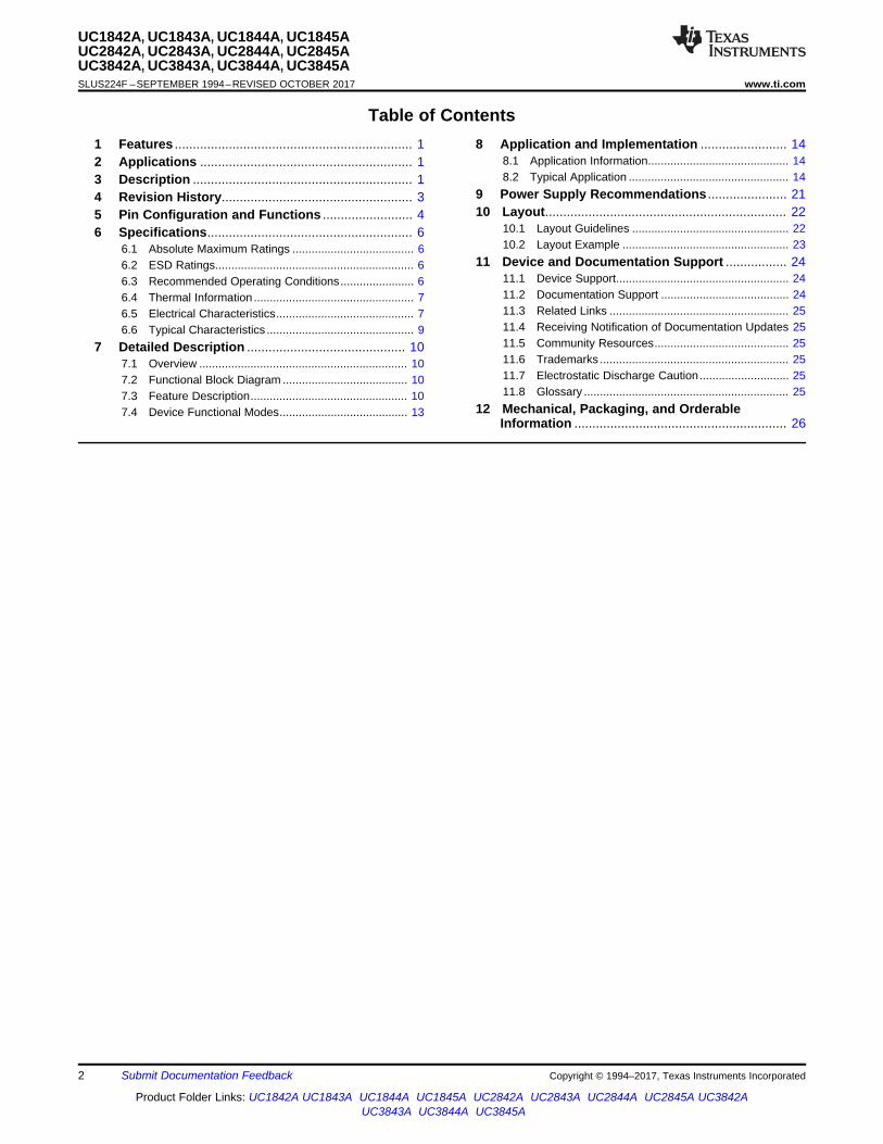
Table of Contents1 Features .................................................................. 12 Applications ........................................................... 13 Description ............................................................. 14 Revision History..................................................... 35 Pin Configuration and Functions ......................... 46 Specifications......................................................... 6
6.1 Absolute Maximum Ratings ...................................... 66.2 ESD Ratings.............................................................. 66.3 Recommended Operating Conditions....................... 66.4 Thermal Information .................................................. 76.5 Electrical Characteristics........................................... 76.6 Typical Characteristics .............................................. 9
7 Detailed Description ............................................ 107.1 Overview ................................................................. 107.2 Functional Block Diagram ....................................... 107.3 Feature Description................................................. 107.4 Device Functional Modes........................................ 13
8 Application and Implementation ........................ 148.1 Application Information............................................ 148.2 Typical Application .................................................. 14
9 Power Supply Recommendations ...................... 2110 Layout................................................................... 22
10.1 Layout Guidelines ................................................. 2210.2 Layout Example .................................................... 23
11 Device and Documentation Support ................. 2411.1 Device Support...................................................... 2411.2 Documentation Support ........................................ 2411.3 Related Links ........................................................ 2511.4 Receiving Notification of Documentation Updates 2511.5 Community Resources.......................................... 2511.6 Trademarks ........................................................... 2511.7 Electrostatic Discharge Caution............................ 2511.8 Glossary ................................................................ 25
12 Mechanical, Packaging, and OrderableInformation ........................................................... 26
3
UC1842A, UC1843A, UC1844A, UC1845AUC2842A, UC2843A, UC2844A, UC2845AUC3842A, UC3843A, UC3844A, UC3845A
www.ti.com SLUS224F –SEPTEMBER 1994–REVISED OCTOBER 2017
Product Folder Links: UC1842A UC1843A UC1844A UC1845A UC2842A UC2843A UC2844A UC2845A UC3842AUC3843A UC3844A UC3845A
Submit Documentation FeedbackCopyright © 1994–2017, Texas Instruments Incorporated
4 Revision HistoryNOTE: Page numbers for previous revisions may differ from page numbers in the current version.
Changes from Revision E (October 2017) to Revision F Page
• Added WEBENCH links in three places, Features, Application and Implementation and Device and DocumentationSupport. .................................................................................................................................................................................. 1
• Added copyright information to the Simplified Application Diagram ...................................................................................... 1• Changed operating free-air temperature of the UC284xA changed from 125°C to 85°C. .................................................... 6• Changed operating free-air temperature of the UC384xA changed from -40°C to 0°C. ....................................................... 6• Changed operating free-air temperature of the UC384xA changed from 85°C to 70°C. ...................................................... 6• Changed the frequency (f) calculation to the correct equation............................................................................................. 13• Changed the COUT equation to the corrected equation. ...................................................................................................... 17• Changed the LPM equation to the corrected equation. ......................................................................................................... 18• Added GCO(f) definition and equation. .................................................................................................................................. 19• Changed the fRHPz equation to the corrected equation......................................................................................................... 19
Changes from Revision D (July 2011) to Revision E Page
• Added Applications section, Device Information table, Pin Configuration and Functions section, Specificationssection, Detailed Description section, Application and Implementation section, Power Supply Recommendationssection, Layout section, Device and Documentation Support section, and Mechanical, Packaging, and OrderableInformation section ................................................................................................................................................................. 1
• Deleted Ordering Information Table; see POA at the end of the datasheet .......................................................................... 1
Changes from Revision C (August 2010) to Revision D Page
• Changed Absolute Maximum ratings table with maximum negative voltage and GND pin notes. ........................................ 6
Changes from Revision B (September 2009) to Revision C Page
• Corrected ISINK voltage............................................................................................................................................................ 8

Not to scale
4NC
5FB
6NC
7ISENSE
8NC
9N
C
10
RT
/CT
11
NC
12
PG
ND
13
GN
D
14 NC
15 OUTPUT
16 NC
17 VC
18 VCC
19
NC
20
VR
EF
1N
C
2C
OM
P
3N
C
Not to scale
1NC 16 NC
2NC 15 VREF
3COMP 14 VCC
4FB 13 VCC
5ISENSE 12 OUTPUT
6RT/CT 11 GND
7NC 10 PGND
8NC 9 NC
Not to scale
1COMP 14 VREF
2NC 13 NC
3FB 12 VCC
4NC 11 VC
5ISENSE 10 OUTPUT
6NC 9 GND
7RT/CT 8 PGND
Not to scale
1COMP 8 VREF
2FB 7 VCC
3ISENSE 6 OUTPUT
4RT/CT 5 GND
4
UC1842A, UC1843A, UC1844A, UC1845AUC2842A, UC2843A, UC2844A, UC2845AUC3842A, UC3843A, UC3844A, UC3845ASLUS224F –SEPTEMBER 1994–REVISED OCTOBER 2017 www.ti.com
Product Folder Links: UC1842A UC1843A UC1844A UC1845A UC2842A UC2843A UC2844A UC2845A UC3842AUC3843A UC3844A UC3845A
Submit Documentation Feedback Copyright © 1994–2017, Texas Instruments Incorporated
5 Pin Configuration and Functions
CDIP, PDIP, and SOIC Packages8-Pin JG, P, and D
Top View
LCCC and PLCC Packages20-Pin FK and FN
Top View
SOIC Package14-Pin DTop View
SOIC Package16-Pin DWTop View

5
UC1842A, UC1843A, UC1844A, UC1845AUC2842A, UC2843A, UC2844A, UC2845AUC3842A, UC3843A, UC3844A, UC3845A
www.ti.com SLUS224F –SEPTEMBER 1994–REVISED OCTOBER 2017
Product Folder Links: UC1842A UC1843A UC1844A UC1845A UC2842A UC2843A UC2844A UC2845A UC3842AUC3843A UC3844A UC3845A
Submit Documentation FeedbackCopyright © 1994–2017, Texas Instruments Incorporated
Pin FunctionsPIN
I/O DESCRIPTIONNAME
NO.CDIP (8),PDIP (8),SOIC (8)
LCCC (20),PLCC (20) SOIC (14) SOIC (16)
COMP 1 2 1 3 O
Outputs the low impedance 1-MHz internal error amplifier that is alsothe input to the peak current limit or PWM comparator, with an open-loop gain (AVOL) of 80 dB. This pin is capable of sinking a maximumof 6 mA and is not internally current limited.
FB 2 5 3 4 I Input to the error amplifier that can be used to control the powerconverter voltage-feedback loop for stability.
GND 5 13 9 11 — This is the controller signal ground.
ISENSE 3 7 5 5 I
Input to the peak current limit, PWM comparator of the UCx84xAcontrollers. When used in conjunction with a current sense resistor,the error amplifier output voltage controls the power systems cycle-by-cycle peak current limit. The maximum peak current sense signalis internally clamped to 1 V. See Functional Block Diagram.
OUTPUT 6 15 10 12 OOutput of 1-A totem pole gate driver. This pin can sink and sourceup to 1 A of gate driver current. A gate driver resistor must be usedto limit the gate driver current.
PGND — 12 8 10 —
Power ground and the gate driver return. For devices that have thispin, star grounding techniques can be used to redirect the gatedriver current away from the signal ground pin (GND). Thistechnique can reduce PWM controller instabilities caused by gatedriver return current.
RT/CT 4 10 7 6 I
Input to the internal oscillator that is programmed with an externaltiming resistor (RT) and timing capacitor (CT). See Oscillator forinformation on properly selecting these timing components. TIrecommends using capacitance values from 470 pF to 4.7 nF. TIalso recommends that the timing resistor values chosen be from5 kΩ to 100 kΩ.
VC — 17 11 — I
Bias input to the gate driver. For PWM controllers that do not havethis pin, the gate driver is biased from the VCC pin. This pin musthave a biasing capacitor that is at least 10 times greater than thegate capacitance of the main switching FET used in the design.
VCC 7 18 12 13, 14 IBias input to the gate driver. This pin must have a biasing capacitorthat is at least 10 times greater than the gate capacitance of themain switching FET used in the design.
VREF 8 20 14 15 O
Reference voltage output of the PWM controller. This pin mustsupply no more than 10 mA under normal operation. This output isshort-circuit protected at roughly 100 mA. This reference is also usedfor internal comparators and needs a high frequency bypasscapacitor of 1 µF. The VCC capacitor also must be at least 10 timesgreater than the capacitor on the VREF pin.
NC —1, 3, 4, 6, 8,
9, 11, 14,16, 19
2, 4, 6, 13 1, 2, 7, 8,9, 16 — No connection

6
UC1842A, UC1843A, UC1844A, UC1845AUC2842A, UC2843A, UC2844A, UC2845AUC3842A, UC3843A, UC3844A, UC3845ASLUS224F –SEPTEMBER 1994–REVISED OCTOBER 2017 www.ti.com
Product Folder Links: UC1842A UC1843A UC1844A UC1845A UC2842A UC2843A UC2844A UC2845A UC3842AUC3843A UC3844A UC3845A
Submit Documentation Feedback Copyright © 1994–2017, Texas Instruments Incorporated
(1) Stresses beyond those listed under Absolute Maximum Ratings may cause permanent damage to the device. These are stress ratingsonly, which do not imply functional operation of the device at these or any other conditions beyond those indicated under RecommendedOperating Conditions. Exposure to absolute-maximum-rated conditions for extended periods may affect device reliability.
6 Specifications
6.1 Absolute Maximum Ratingsover operating free-air temperature range (unless otherwise noted) (1)
MIN MAX UNITSupply voltage (low impedance source) VCC pin 30 VOutput current, IOUT ±1 AOutput energy (capacitive load) 5 µJAnalog inputs –0.3 6.3 VMaximum negative voltage All pins –0.3 VDifferential voltage between VC and VCC VC pin –0.3 VError amplifier output sink current, ICOMP 10 mAPower dissipation at TA ≤ 25°C 1 WLead temperature (soldering, 10 s) 300 °CJunction temperature, TJ –55 150 °CStorage temperature, Tstg –65 150 °C
(1) JEDEC document JEP155 states that 500-V HBM allows safe manufacturing with a standard ESD control process.(2) JEDEC document JEP157 states that 250-V CDM allows safe manufacturing with a standard ESD control process.
6.2 ESD RatingsVALUE UNIT
V(ESD) Electrostatic dischargeHuman-body model (HBM), per ANSI/ESDA/JEDEC JS-001 (1) ±2000
VCharged-device model (CDM), per JEDEC specification JESD22-C101 (2) ±1500
6.3 Recommended Operating Conditionsover operating free-air temperature range (unless otherwise noted)
MIN NOM MAX UNITVCC Bias supply voltage VCC pin 11 VVFB, VRC, VVFB Voltage on analog pins FB, ISENSE, and RT/CT pins –0.1 5 VVOUT Gate driver output voltage –0.1 VCC VIVCC Supply bias current 25 mAIVREF Output current VREF pin 10 mAfOSC Oscillator frequency 500 kHz
TA Operating free-air temperatureUC184xA –55 125
°CUC284xA –40 85UC384xA 0 70

7
UC1842A, UC1843A, UC1844A, UC1845AUC2842A, UC2843A, UC2844A, UC2845AUC3842A, UC3843A, UC3844A, UC3845A
www.ti.com SLUS224F –SEPTEMBER 1994–REVISED OCTOBER 2017
Product Folder Links: UC1842A UC1843A UC1844A UC1845A UC2842A UC2843A UC2844A UC2845A UC3842AUC3843A UC3844A UC3845A
Submit Documentation FeedbackCopyright © 1994–2017, Texas Instruments Incorporated
(1) For more information about traditional and new thermal metrics, see the Semiconductor and IC Package Thermal Metrics applicationreport.
6.4 Thermal Information
THERMAL METRIC (1)UC184xA UC2843A UC284xA, UC384xA
UNITJG (CDIP) FK (LCCC) FN (PLCC) P (PDIP) D (SOIC) D (SOIC) DW (SOIC)8 PINS 20 PINS 20 PINS 8 PINS 8 PINS 14 PINS 16 PINS
RθJAJunction-to-ambient thermalresistance — — 56.7 53.4 104.3 77.9 73.6 °C/W
RθJC(top)Junction-to-case (top)thermal resistance 64 36.2 34.6 46.4 46.8 35.8 35 °C/W
RθJBJunction-to-board thermalresistance 92.5 35.4 21.8 30.7 45.3 32.5 38.4 °C/W
ψJTJunction-to-topcharacterization parameter — — 10.4 16.8 6 6.6 9.7 °C/W
ψJBJunction-to-boardcharacterization parameter — — 21.5 30.6 44.6 32.2 37.8 °C/W
RθJC(bot)Junction-to-case (bottom)thermal resistance 15.1 4.1 — — — — — °C/W
(1) Adjust VCC above the start threshold before setting at 15 V.(2) Ensured by design, but not 100% production tested.(3) Temperature stability, sometimes referred to as average temperature coefficient, is described by: Temperature stability = ( VREF(max) –
VREF(min)) / (TJ(max) – TJ(min) ). VREF(max) and VREF(min) are the maximum and minimum reference voltage measured over the appropriatetemperature range. Note that the extremes in voltage do not necessarily occur at the extremes in temperature.
(4) Output frequency equals oscillator frequency for the UC1842A and UC1843A. Output frequency is one half oscillator frequency for theUC1844A and UC1845A.
(5) This parameter is measured with RT = 10 kΩ to VREF. This contributes approximately 300 µA of current to the measurement. The totalcurrent flowing into the RT/CT pin is approximately 300 µA higher than the measured value.
6.5 Electrical CharacteristicsUnless otherwise stated, these specifications apply for TA = –55°C to 125°C (UC184xA), TA = –40°C to 125°C (UC284xAQ),TA = –40°C to 85°C (UC284xA), TA = 0°C to 70°C (UC384xA); TA = TJ; VCC = 15 V (1); RT = 10 kΩ; CT = 3.3 nF.
PARAMETER TEST CONDITIONS MIN TYP MAX UNITREFERENCE
Output voltage TJ = 25°C, IO = 1 mAUC184xA, UC284xA 4.95 5 5.05
VUC384xA 4.9 5 5.1
Line regulation 12 ≤ VIN ≤ 25 V 6 20 mVLoad regulation 1 ≤ IO ≤ 20 mA 6 25 mVTemperature stability See (2) (3) 0.2 0.4 mV/°C
Total output variation Line, Load, TemperatureUC184xA, UC284xA 4.9 5.1
VUC384xA 4.82 5.18
Output noise voltage 10 Hz ≤ f ≤ 10 kHz; TJ = 25°C (2) 50 µVLong-term stability TA = 125°C, 1000 hrs (2) 5 25 mVOutput short circuit –30 –100 –180 mA
OSCILLATORInitial accuracy TJ = 25°C (4) 47 52 57 kHzVoltage stability 12 ≤ VCC ≤ 25 V 0.2% 1%Temperature stability TMIN ≤ TA ≤ TMAX
(2) 5%Amplitude VRT/CT peak to peak (2) 1.7 V
Discharge currentTJ = 25°C, VRT/CT = 2 V (5) 7.8 8.3 8.8
mAVRT/CT = 2 V (5) UC184xA, UC284xA 7.5 8.8
UC384xA 7.6 8.8

8
UC1842A, UC1843A, UC1844A, UC1845AUC2842A, UC2843A, UC2844A, UC2845AUC3842A, UC3843A, UC3844A, UC3845ASLUS224F –SEPTEMBER 1994–REVISED OCTOBER 2017 www.ti.com
Product Folder Links: UC1842A UC1843A UC1844A UC1845A UC2842A UC2843A UC2844A UC2845A UC3842AUC3843A UC3844A UC3845A
Submit Documentation Feedback Copyright © 1994–2017, Texas Instruments Incorporated
Electrical Characteristics (continued)Unless otherwise stated, these specifications apply for TA = –55°C to 125°C (UC184xA), TA = –40°C to 125°C (UC284xAQ),TA = –40°C to 85°C (UC284xA), TA = 0°C to 70°C (UC384xA); TA = TJ; VCC = 15 V(1); RT = 10 kΩ; CT = 3.3 nF.
PARAMETER TEST CONDITIONS MIN TYP MAX UNIT
(6) Parameter measured at trip point of latch with VFB = 0.(7) Gain defined as: A = ΔVCOMP / ΔVISENSE; 0 ≤ VISENSE ≤ 0.8 V.
ERROR AMPLIFIER
Input voltage VCOMP = 2.5 VUC184xA, UC284xA 2.45 2.5 2.55
VUC384xA 2.42 2.5 2.58
Input bias current–0.3 –1
µA–0.3 –2
AVOL Open-loop gain 2 ≤ VO ≤ 4 V 65 90 dBUnity gain bandwidth TJ = 25°C (2) 0.7 1 MHz
CMRR Common mode rejection ratio 12 ≤ VCC ≤ 25 V 60 70 dBOutput sink current VFB = 2.7 V, VCOMP = 1.1 V 2 6 mAOutput source current VFB = 2.3 V, VCOMP = 5 V –0.5 –0.8 mAVOUT high VFB = 2.3 V, RL = 15 kΩ to ground 5 6 VVOUT low VFB = 2.7 V, RL = 15 kΩ to VREF 0.7 1.1 V
CURRENT SENSEGain See (6) (7) 2.85 3 3.15 V/VMaximum input signal VCOMP = 5 V (6) 0.9 1 1.1 V
PSRR Power supply rejection ratio 12 ≤ VCC 25 V (6) 70 dBInput bias current –2 –10 µADelay to output VISENSE = 0 to 2 V (2) 150 300 ns
OUTPUT
Output low levelISINK = 20 mA 0.1 0.4
VISINK = 200 mA 15 2.2
Output high levelISOURCE = 20 mA 13 13.5
VISOURCE = 200 mA 12 13.5
Rise time TJ = 25°C, CL = 1 nF (2) 50 150 nsFall time TJ = 25°C, CL = 1 nF (2) 50 150 nsUVLO saturation VCC = 5 V, ISINK = 10 mA 0.7 1.2 V
UNDERVOLTAGE LOCKOUT
Start thresholdUC1842A, UC1844A, UC2842A, and UC2844A 15 16 17
VUC3842A and UC3844A 14.5 16 17.5UCx843A and UCx845A 7.8 8.4 9
Minimum operation voltage afterturnon
UC1842A, UC1844A, UC2842A, and UC2844A 9 10 11VUC3842A and UC3844A 8.5 10 11.5
UCx843A and UCx845A 7 7.6 8.2PWM
Maximum duty cycleUCx842A, UCx843A 94% 96% 100%UCx844A, UCx845A 47% 48% 50%
Minimum duty cycle 0%TOTAL STANDBY CURRENT
Start-up current 0.3 0.5 mAOperating supply current VFB = VISENSE = 0 V 11 17 mAVCC Zener voltage ICC = 25 mA 30 34 V

9
UC1842A, UC1843A, UC1844A, UC1845AUC2842A, UC2843A, UC2844A, UC2845AUC3842A, UC3843A, UC3844A, UC3845A
www.ti.com SLUS224F –SEPTEMBER 1994–REVISED OCTOBER 2017
Product Folder Links: UC1842A UC1843A UC1844A UC1845A UC2842A UC2843A UC2844A UC2845A UC3842AUC3843A UC3844A UC3845A
Submit Documentation FeedbackCopyright © 1994–2017, Texas Instruments Incorporated
6.6 Typical Characteristics
Figure 1. Output Saturation Characteristics Figure 2. Error Amplifier Open-Loop Frequency Response

S(max)S
1 VI
R´
VREF5 V
VC
OUTPUT
GND
PWMLatch
CurrentSense
Comparator
1 VR
2RErrorAmp
ISENSE
COMP
FB
RT/CT
GND
VCC
34 V
2.5 V
UVLO
+
–
T
S
R
VREFGoodLogic
InternalBias
5 VREF
S/R
OSC
Copyright © 2016, Texas Instruments Incorporated
10
UC1842A, UC1843A, UC1844A, UC1845AUC2842A, UC2843A, UC2844A, UC2845AUC3842A, UC3843A, UC3844A, UC3845ASLUS224F –SEPTEMBER 1994–REVISED OCTOBER 2017 www.ti.com
Product Folder Links: UC1842A UC1843A UC1844A UC1845A UC2842A UC2843A UC2844A UC2845A UC3842AUC3843A UC3844A UC3845A
Submit Documentation Feedback Copyright © 1994–2017, Texas Instruments Incorporated
7 Detailed Description
7.1 OverviewThe UCx84xA family of fixed-frequency pulse-width-modulator (PWM) controllers are designed to operate atswitching frequencies of 500 kHz. These controllers are designed for peak current mode (PCM) and can be usedin isolated and non-isolated power supply designs. These controllers can drive FETs directly from the output,which is capable of sourcing and sinking up to 1 A of gate driver current. These devices also have a built-in low-impedance amplifier that can be used in non-isolated designs to control the power supply output voltage andfeedback loop.
7.2 Functional Block Diagram
7.3 Feature Description
7.3.1 Pulse-by-Pulse Current LimitingPulse-by-pulse limiting is inherent in the current mode control scheme. An upper limit on the peak current can beestablished by simply clamping the error voltage. Accurate current limiting allows optimization of magnetic andpower semiconductor elements while ensuring reliable supply operation.
7.3.2 Current Sense CircuitPeak current (IS) is determined by Equation 1:
(1)
A small RC filter may be required to suppress switch transients.

11
UC1842A, UC1843A, UC1844A, UC1845AUC2842A, UC2843A, UC2844A, UC2845AUC3842A, UC3843A, UC3844A, UC3845A
www.ti.com SLUS224F –SEPTEMBER 1994–REVISED OCTOBER 2017
Product Folder Links: UC1842A UC1843A UC1844A UC1845A UC2842A UC2843A UC2844A UC2845A UC3842AUC3843A UC3844A UC3845A
Submit Documentation FeedbackCopyright © 1994–2017, Texas Instruments Incorporated
Feature Description (continued)
Figure 3. Current Sense Circuit Diagram
7.3.3 Error Amplifier ConfigurationThe error amplifier can source up to 0.8 mA, and sink up to 6 mA.
Figure 4. Error Amplifier Configuration Diagram
7.3.4 Undervoltage LockoutThe UCx84xA devices feature undervoltage lockout protection circuits for controlled operation during power-upand power-down sequences. Undervoltage lockout thresholds for the UCx842A, UCx843A, UCx844A, andUCx845A devices are optimized for two groups of applications: off-line power supplies and DC-DC converters.With a wider VCCON to VCCOFF range, the UCx842A and UCx844A devices are ideally suited to off-line AC inputapplications. The UCx843A and UCx845A controllers have a much narrower VCCON to VCCOFF hysteresis andmay be used in DC to DC applications where the input is considered regulated.
During UVLO the IC draws typically 0.3 mA of supply current. This VCC current is considerable less than theUCx84x family and results in lower power drawn from the line. The reduced start-up current is of particularconcern in off-line supplies where the IC is powered-up from the high-voltage DC rail, then bootstrapped to anauxiliary winding on the main transformer. Power is then dissipated in the start-up resistor which is sized by theIC’s start-up current. Lowering this by 50% in the UCx84xA version family, as compared to the UCx84x family,reduces the resistors power loss by the same percentage. Once crossing the turnon threshold the IC supplycurrent increases typically to about 11 mA, During undervoltage lockout, the UCx84xA series of devices preventthe power MOSFET from parasitically turning on due to the Miller effect at power-up. This improved design to thelower totem-pole transistor’s operation during undervoltage lockout allows the IC to sink higher currents, up to 10mA, at saturation voltages as low as 0.7 V, compared to the UCx84x devices which would only sink up to 0.2 mAunder the same conditions.

470 pF
1 nF
2.2 nF
4.7nF
CT
300 1 k 3 k 10 k 30 k 100 k
R (T Ω)
1 M
100 k
10 k
Oscill
ato
r F
requency (
Hz)
300 1 k 3 k 10 k 30 k 100 k
R (T Ω)
100
80
60
40
20
Ma
xim
um
Du
ty C
ycle
(%
)
During UVLO, the Output is low.
12
UC1842A, UC1843A, UC1844A, UC1845AUC2842A, UC2843A, UC2844A, UC2845AUC3842A, UC3843A, UC3844A, UC3845ASLUS224F –SEPTEMBER 1994–REVISED OCTOBER 2017 www.ti.com
Product Folder Links: UC1842A UC1843A UC1844A UC1845A UC2842A UC2843A UC2844A UC2845A UC3842AUC3843A UC3844A UC3845A
Submit Documentation Feedback Copyright © 1994–2017, Texas Instruments Incorporated
Feature Description (continued)
Figure 5. Undervoltage Lockout
7.3.5 Oscillator
Figure 6. Oscillator Frequency vs Timing Resistance Figure 7. Maximum Duty Cycle vs Timing Resistance

8
4
5
RT
CT
ô�� �� > Þ � � NÚ.àÛ
�� × ñ�
13
UC1842A, UC1843A, UC1844A, UC1845AUC2842A, UC2843A, UC2844A, UC2845AUC3842A, UC3843A, UC3844A, UC3845A
www.ti.com SLUS224F –SEPTEMBER 1994–REVISED OCTOBER 2017
Product Folder Links: UC1842A UC1843A UC1844A UC1845A UC2842A UC2843A UC2844A UC2845A UC3842AUC3843A UC3844A UC3845A
Submit Documentation FeedbackCopyright © 1994–2017, Texas Instruments Incorporated
Feature Description (continued)
Figure 8. Oscillator Section Figure 9. Slope Compensation
Precision operation at high frequencies with an accurate maximum duty cycle, see Figure 7, can now beobtained with the UCx84xA family of devices due to its trimmed oscillator discharge current. This nullifies theeffects of production variations in the initial discharge current or dead time. Previous versions of the UCx84xdevices had greater than a 2:1 oscillator discharge current range and resulted in less reliable maximum dutycycle programming.
A fraction of the oscillator ramp can be resistively summed with the current sense signal, to provide slopecompensation for converters requiring duty cycles over 50%. Capacitor C forms a filter with R2 to suppress theleading-edge switch spikes.
7.4 Device Functional Modes
7.4.1 Normal OperationThe IC can be used in peak current mode (PCM) control or voltage mode (VM) control. When the converter isoperating in PCM, the voltage amplifier output will regulate the converter's peak current and duty cycle. When theIC is used in VM control, the voltage amplifier output will regulate the power converter's duty cycle. Theregulation of the system's peak current and duty cycle can be achieved with the use of the integrated erroramplifier and external feedback circuitry.
7.4.2 Undervoltage Lockout (UVLO) Start-UpDuring system start-up, VCC voltage starts to rise from 0. Before the VCC voltage reaches its correspondingstart threshold, the IC is operating in UVLO mode. After the UVLO turn start-up threshold is met the device willbecome active and the reference will come up to 5 V.
7.4.3 UVLO Turnoff ModeIf the bias voltage to VCC drops below the UVLO minimum operating voltage, PWM switching stops and thereference will become inactive, returning to 0 V. The device can be restarted by applying a voltage greater thanthe UVLO start threshold to the VCC pin.

14
UC1842A, UC1843A, UC1844A, UC1845AUC2842A, UC2843A, UC2844A, UC2845AUC3842A, UC3843A, UC3844A, UC3845ASLUS224F –SEPTEMBER 1994–REVISED OCTOBER 2017 www.ti.com
Product Folder Links: UC1842A UC1843A UC1844A UC1845A UC2842A UC2843A UC2844A UC2845A UC3842AUC3843A UC3844A UC3845A
Submit Documentation Feedback Copyright © 1994–2017, Texas Instruments Incorporated
8 Application and Implementation
NOTEInformation in the following applications sections is not part of the TI componentspecification, and TI does not warrant its accuracy or completeness. TI’s customers areresponsible for determining suitability of components for their purposes. Customers shouldvalidate and test their design implementation to confirm system functionality.
8.1 Application InformationThe UCx84xA controllers are peak-current mode pulse-width modulators. These controllers have an onboardamplifier and can be used in isolated or nonisolated power supply designs. There is an onboard totem-pole gatedriver capable of delivering 1 A of peak current. This is a high-speed PWM capable of operating at switchingfrequencies up to 500 kHz.
8.2 Typical ApplicationA typical application for the UC3842A in an off-line flyback converter is shown in Figure 10. The UC3842A usesan inner current control loop that contains a small current sense resistor which senses the primary inductorcurrent ramp. This current sense resistor transforms the inductor current waveform to a voltage signal that isinput directly into the primary side PWM comparator. This inner loop determines the response to input voltagechanges. An outer voltage control loop involves comparing a portion of the output voltage to a reference voltageat the input of an error amplifier. When used in an off-line isolated application, the voltage feedback of theisolated output is accomplished using a secondary-side error amplifier and adjustable voltage reference, such asthe TL431. The error signal crosses the primary to secondary isolation boundary using an opto-isolator whosecollector is connected to the VREF pin and the emitter is connected to FB. The outer voltage control loopdetermines the response to load changes.

DCL
~
~
+–
CIN
QA
DC
VOUT+
VOUT–
RCS
1
2
3
4
8
7
6
5
COMP
FB
ISENSE OUTPUT
RT/CT GND
VCC
VREF
C
1 µFVCC1 C
1 µFVREF
NP
RH
DB
NA
RD
22 Ω
CT
RT
V = 85 V to 265 V ACIN
CF
RS2
270 pF
UC3842A
RG
RA 10 kΩ
RC 1 kΩ
RZ
CZ
RI
RK
U1
U2
RE 1 kΩ
DC
U3
FA
DA
RB
4.99 kΩ
CA 1 nF
RS1
CS1
RP
200 kΩ
RJ 1 kΩ
300 kΩ
10 nF
10 Ω
CP
10 V
5 ACCL
RCL 50 kΩ10 nF
2.05 kΩ
TL431
1 kΩ
RF
VA
120 µFCVCC2
RAC
VO
V ’O
VB
VC
Copyright © 2016, Texas Instruments Incorporated
15
UC1842A, UC1843A, UC1844A, UC1845AUC2842A, UC2843A, UC2844A, UC2845AUC3842A, UC3843A, UC3844A, UC3845A
www.ti.com SLUS224F –SEPTEMBER 1994–REVISED OCTOBER 2017
Product Folder Links: UC1842A UC1843A UC1844A UC1845A UC2842A UC2843A UC2844A UC2845A UC3842AUC3843A UC3844A UC3845A
Submit Documentation FeedbackCopyright © 1994–2017, Texas Instruments Incorporated
Typical Application (continued)
Figure 10. Typical Flyback Application Circuit

( )
BULK(min)OUT
IN(min)
VP 1
2 V
IN 2 2IN(min) BULK(min) LINE
2 0.25 arcsin
C 180 µF2 V V f
h p ´
é ùæ ö´ ´ + ´ ´ ç ÷ê úè øë û= »
´ - ´
( )
BULK(min)OUT
IN(min)
VP 1
2 V
INripple 2 2IN(min) BULK(min) LINE
2 0.25 arcsin
V2 V V f
h p ´
é ùæ ö´ ´ + ´ ´ ç ÷ê úè øë û=
´ - ´
16
UC1842A, UC1843A, UC1844A, UC1845AUC2842A, UC2843A, UC2844A, UC2845AUC3842A, UC3843A, UC3844A, UC3845ASLUS224F –SEPTEMBER 1994–REVISED OCTOBER 2017 www.ti.com
Product Folder Links: UC1842A UC1843A UC1844A UC1845A UC2842A UC2843A UC2844A UC2845A UC3842AUC3843A UC3844A UC3845A
Submit Documentation Feedback Copyright © 1994–2017, Texas Instruments Incorporated
Typical Application (continued)8.2.1 Design RequirementsFor this design example, use the parameters listed in Table 1 as the input parameters.
Table 1. Design ParametersPARAMETER MIN TYP MAX UNIT
INPUT CHARACTERISTICSVIN Input voltage (RMS) 85 265 VfLINE Line frequency 47 63 HzOUTPUT CHARACTERISTICSVOUT Output voltage 11.75 12 12.25 V
Output ripple voltage 50 mVPP
IOUT Output current 4 4.33 ALoad step 11.75 12.25 V
SYSTEMS CHARACTERISTICSη Maximum load efficiency 86%
8.2.2 Detailed Design Procedure
8.2.2.1 Custom Design With WEBENCH® ToolsClick here to create a custom design using the UCx84xA device with the WEBENCH® Power Designer.1. Start by entering the input voltage (VIN), output voltage (VOUT), and output current (IOUT) requirements.2. Optimize the design for key parameters such as efficiency, footprint, and cost using the optimizer dial.3. Compare the generated design with other possible solutions from Texas Instruments.
The WEBENCH Power Designer provides a customized schematic along with a list of materials with real-timepricing and component availability.
In most cases, these actions are available:• Run electrical simulations to see important waveforms and circuit performance• Run thermal simulations to understand board thermal performance• Export customized schematic and layout into popular CAD formats• Print PDF reports for the design, and share the design with colleagues
Get more information about WEBENCH tools at www.ti.com/WEBENCH.
8.2.2.2 UC2842A Design ProcedureThis application design procedure shows how to setup and use the UC2842A peak current mode controller in anoffline flyback converter, with universal input to a 12-V, 48-W regulated output.
Setting up and designing with the UC2842A peak current mode controller in a continuous mode flybackapplication requires knowing some things about the power stage. First, calculate the required input bulkcapacitance (CIN) based on output power level (POUT), efficiency (ƞ), minimum input voltage (VIN(min)), linefrequency (fLINE) and minimum bulk voltage. For this design example let VBULK(min) = 95 V.
(2)
(3)

IN(min)PS
OUT
V 2 85 V 2N 10
V 12 V
´ ´£ = »
COUT R
IOUTfC
VOUT × 10%N 1.33mF
17
UC1842A, UC1843A, UC1844A, UC1845AUC2842A, UC2843A, UC2844A, UC2845AUC3842A, UC3843A, UC3844A, UC3845A
www.ti.com SLUS224F –SEPTEMBER 1994–REVISED OCTOBER 2017
Product Folder Links: UC1842A UC1843A UC1844A UC1845A UC2842A UC2843A UC2844A UC2845A UC3842AUC3843A UC3844A UC3845A
Submit Documentation FeedbackCopyright © 1994–2017, Texas Instruments Incorporated
The output capacitor (COUT) is sized so the output voltage does not droop more than 10% during a large-signaltransient response. The voltage-loop crossover frequency (fC) is estimated to be 2.5 kHz at this point in thedesign.
(4)
The COUT selected for the design is a 2200-µF capacitor, with an equivalent series resistance (ESR) of 45 mΩ.
Next calculate the maximum primary to secondary turns ratio (NPS) of the transformer, based on the minimuminput voltage and output voltage.
(5)

Pf 5 kHz=
s(f ) 2 1i f= ´ p ´ ´
( ) ( )K OUT TL431REF
I
TL431REF
R V V 2.49 k 12 V 2.5 VR 9.462 k 9.53 k
V 2.5 V
´ - W ´ -= = = W » W
S2R 2.05 k= W
( )
( )S2 SW SM PS
S1 S2
OUT CS
1.7 V R f 2 L NR R 27.72 k 27.4 k
V 1 D R
´ ´ ´ ´ ´= - = W » W
´ - ´
CSLpPK
1 VR 0.725 0.75
I 1.3= = W » W
´
( )OUT LM
LpPKPS
I II 1.1 A
N 1 D 2= + »
´ -
BULK(min)LPM
SW M
V DI 0.31 A
f L
´
= »
´
LPM RVBULK :min ; ×D
70%× IOUT × fswD×NPS
= 1.632mH N 1.7mH
PS OUT
BULK(min) PS OUT
N VD 0.56
V N V
´
= »
+ ´
VCCAS
OUT
V 12 VN 1
V 12 V£ = =
18
UC1842A, UC1843A, UC1844A, UC1845AUC2842A, UC2843A, UC2844A, UC2845AUC3842A, UC3843A, UC3844A, UC3845ASLUS224F –SEPTEMBER 1994–REVISED OCTOBER 2017 www.ti.com
Product Folder Links: UC1842A UC1843A UC1844A UC1845A UC2842A UC2843A UC2844A UC2845A UC3842AUC3843A UC3844A UC3845A
Submit Documentation Feedback Copyright © 1994–2017, Texas Instruments Incorporated
Next calculate the auxiliary to secondary turns ratio (NAS) of the transformer, based on the output voltage and thebias voltage of the UC2842A.
(6)
Once the transformer turns ratios have been determined, the minimum primary magnetizing inductance (LPM) ofthe transformer can be calculated based on minimum bulk voltage, Duty Cycle (D), reflected output current andefficiency. The transformer used in this design has an LPM of 1.7 mH, NPS = 10, and a NAS = 1, fsw = 100 kHz
(7)
(8)
After the transformer has been selected, the primary peak current (ILpPK) of the transformer can be calculatedbased on the primary magnetizing inductance ripple (ILPM) and the reflected output current across thetransformer.
(9)
(10)
Once the primary peak current has been calculated the current sense resistor (RCS) can be selected.
(11)
Resistors RS1 and RS2 are used to set the slope compensation of the design. Capacitor CS1 is a DC blockingcapacitor, and pull-up resistor RP is used to provide some offset to the current sense signal for noise immunity.RP and RS2 were preselected to add a DC offset of 50 mV to the current sense signal.
RS1 is selected to set the slope compensation to one-half of the ripple current down slope of the flyback inductor.This can be accomplished by calculating the secondary magnetizing inductance (LSM) and using the followingcalculation for RS1. The 1.7 V in the RS1 equation is the peak-to-peak ripple voltage amplitude of the oscillator.
where• (12)
Resistors RI and RK are selected to the output reference and can be calculated by preselecting a value for RKand knowing the TL431 reference voltage (VTL431REF). After choosing 2.49 kΩ for RK, RI is calculated and astandard resistor value of 9.53 kΩ is chosen for this resistor.
(13)
This design using the UC2842A controller has an interesting control loop with many components. GOPTO(f) is theapproximate transfer function across the opto isolator in the design. The pole frequency of the opto isolator isrepresented by fP. The opto isolator used in this design has a current transfer ratio of 1 and pole frequency ofroughly 5 kHz. See Figure 10 for component placement and node voltages. The voltage loop (fC) must cross-over less than the opto isolator pole for simplified compensation.
(14)
(15)

ZP
CC 680 pF
10= =
CZ f
Z5
1C 6.7 nF
2 R
= »
p ´ ´
( ) ( ) ( )I
Z
OPTO C BC C O CO C
RR 23.95 k , a 23.7 k was used
G f / 5 G f / 5 G G f / 5= = W W
´ ´ ´
RHPzC
ff 5 kHZ
2£ »
B4*2V =:025;
2
2 × è × .LI4176
&:1F &;2
N 9.8G*V
( ) ( )E
N
S
S
1Q
1 1 D 0.5
=é ùp + ´ - -ê úë û
S2 SWE
S1 S2
R fS 1.7 V
R R
´
= ´
+
BULK CSN
PM
V RS
L
´
=
)%1:B; = Â8176
Â8%= 025 ×
1F&
1 +&× HO:B;× '54 × %176 + 1O:B;×4176 × %176 + 1I× H1F O:B;.5/ ×&
4176 × :1F&;2I×1
3
1 +O:B;
2 × è×B59 ×
23+L O:B;
2× è ×B592
M2
PS OUT
BULK PS OUT
N VD 0.24 to 0.56
V N V
´
= =
+ ´
C ABC
B B A A
V R 1G (f )
V R s(f ) R C 1
D= = ´
D ´ ´ +
P
CBOPTO s(f )
A F 2 f
RV ctrG (f )
V R 1´p´
D= = ´
D +
19
UC1842A, UC1843A, UC1844A, UC1845AUC2842A, UC2843A, UC2844A, UC2845AUC3842A, UC3843A, UC3844A, UC3845A
www.ti.com SLUS224F –SEPTEMBER 1994–REVISED OCTOBER 2017
Product Folder Links: UC1842A UC1843A UC1844A UC1845A UC2842A UC2843A UC2844A UC2845A UC3842AUC3843A UC3844A UC3845A
Submit Documentation FeedbackCopyright © 1994–2017, Texas Instruments Incorporated
(16)
GBC(f) is an estimate of the transfer function from the output of the opto isolator to the PWM’s control voltage.
(17)
The duty cycle varies with the bulk input voltage (VBULK). VBULK varies from 95 V to 375 V during normaloperation. This causes the duty cycle to vary from 24% to 56%.
(18)
GCO(f) is an estimate of the control (VC) to output transfer function, where variable Q is the quality factor.
(19)
The quality factor (Q) is defined by the primary magnetizing inductance change in voltage (SN) as a function ofduty cycle; as well as, the added slope compensation (SE).
(20)
(21)
(22)
To ensure that the voltage loop is stable, the crossover frequency must be less than one half of the right-half-plane zero frequency (fRHPZ) of the flyback converter. The right-half-plane zero frequency at the minimum bulkvoltage would be roughly 9.8 kHz. For this design example the target crossover of the voltage loop is at 1 kHz.The actual fC may be higher or lower than the target.
(23)
(24)
The DC gain of GCO(f) moves with the bulk input voltage. Resistor RZ is selected to crossover the voltage loopwhen input to the converter is at VBULK(min) and to crossover at 1/5th the maximum crossover frequency.
(25)
Capacitor CZ is selected to add 45° of phase margin at voltage loop crossover. For this design example a 6.8-nFcapacitor was used.
(26)
Capacitor CP is selected to attenuate the high frequency gain of the control loop.
(27)
GC(f) is the estimated transfer function of the TL431 compensation.

( ) ( )Z Z P
Z P
C Z ZC s(f ) R C C
O I Z P C C
V s(f ) R C 1G (f )
V ' s(f ) R C C 1´ ´ ´
+
D ´ ´ += =
D ´ ´ + ´ +
20
UC1842A, UC1843A, UC1844A, UC1845AUC2842A, UC2843A, UC2844A, UC2845AUC3842A, UC3843A, UC3844A, UC3845ASLUS224F –SEPTEMBER 1994–REVISED OCTOBER 2017 www.ti.com
Product Folder Links: UC1842A UC1843A UC1844A UC1845A UC2842A UC2843A UC2844A UC2845A UC3842AUC3843A UC3844A UC3845A
Submit Documentation Feedback Copyright © 1994–2017, Texas Instruments Incorporated
(28)
Frequency
Gai
n (d
B)
Pha
se (
°)
-100 -200
-75 -150
-50 -100
-25 -50
0 0
25 50
50 100
75 150
100 200
1 10 100 1k 10k 100k
D001
Tv(f)TTv(f)
Frequency
Gai
n (d
B)
Pha
se (
°)
-100 -200
-75 -150
-50 -100
-25 -50
0 0
25 50
50 100
75 150
100 200
1 10 100 1k 10k 100k
D001
Tvd(f)TTv(f)
V C OPTO BC O CO CT (f ) G (f ) G (f ) G (f ) G G (f )= ´ ´ ´ ´
21
UC1842A, UC1843A, UC1844A, UC1845AUC2842A, UC2843A, UC2844A, UC2845AUC3842A, UC3843A, UC3844A, UC3845A
www.ti.com SLUS224F –SEPTEMBER 1994–REVISED OCTOBER 2017
Product Folder Links: UC1842A UC1843A UC1844A UC1845A UC2842A UC2843A UC2844A UC2845A UC3842AUC3843A UC3844A UC3845A
Submit Documentation FeedbackCopyright © 1994–2017, Texas Instruments Incorporated
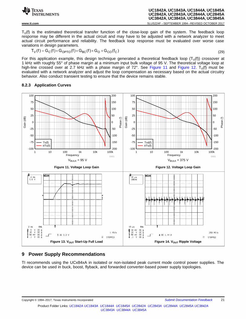
TV(f) is the estimated theoretical transfer function of the close-loop gain of the system. The feedback loopresponse may be different in the actual circuit and may have to be adjusted with a network analyzer to meetactual circuit performance and reliability. The feedback loop response must be evaluated over worse casevariations in design parameters.
(29)
For this application example, this design technique generated a theoretical feedback loop (TV(f)) crossover at1 kHz with roughly 55° of phase margin at a minimum input bulk voltage of 95 V. The theoretical voltage loop athigh-line crossed over at 2.7 kHz with a phase margin of 72°. See Figure 11 and Figure 12. TV(f) must beevaluated with a network analyzer and adjust the loop compensation as necessary based on the actual circuitrybehavior. Also conduct transient testing to ensure that the device remains stable.
8.2.3 Application Curves
VBULK = 95 V
Figure 11. Voltage Loop Gain
VBULK = 375 V
Figure 12. Voltage Loop Gain
Figure 13. VOUT Start-Up Full Load Figure 14. VOUT Ripple Voltage
9 Power Supply RecommendationsTI recommends using the UCx84xA in isolated or non-isolated peak current mode control power supplies. Thedevice can be used in buck, boost, flyback, and forwarded converter-based power supply topologies.

22
UC1842A, UC1843A, UC1844A, UC1845AUC2842A, UC2843A, UC2844A, UC2845AUC3842A, UC3843A, UC3844A, UC3845ASLUS224F –SEPTEMBER 1994–REVISED OCTOBER 2017 www.ti.com
Product Folder Links: UC1842A UC1843A UC1844A UC1845A UC2842A UC2843A UC2844A UC2845A UC3842AUC3843A UC3844A UC3845A
Submit Documentation Feedback Copyright © 1994–2017, Texas Instruments Incorporated
10 Layout
10.1 Layout Guidelines• Star grounding techniques must be used.• Current loops must be kept as short and narrow as possible.• The IC ground and power ground must meet at the return for the input bulk capacitor. Ensure that high
frequency and high current from the power stage does not go through the signal ground paths.• A high-frequency bypass capacitor (CVCC1) must be placed across VCC and GND pins as close as possible to
the pins.• Resistor RS2 and capacitor CF form a low-pass filter for the current sense signal. CF must be as close to CS
and GND pins as possible.• Capacitor CVREF must be as close to VREF and GND pins as possible.• Figure 15 shows the SMD components arranged for wave-solder on a single-layer board. If multiple layers
are used, some components may be rearranged for easier interconnection and reduced current-loop areas. Ifthe solder process allows, placing the SMD components in perpendicular orientations may improveinterconnections and loop areas.

TO-220FP Bottom View
REF
OUT
GND
COMP
CS
FB
RC
VCCUC2842A
RT
CT
CREF
RG
RCS1
RCS2Track To
Transformer =>
Track To
<= �µol�����5
MOSFET Heatsink
S
D
G
Wav
e S
olde
r D
irect
ion
==>
Track To
<= Bulk Cap +
TR
AN
SF
OR
ME
R
6
4
1
2
AU
X W
inding½
PR
I Winding
½ P
RI W
inding
22AWG
Jumper
Wire
22AWG Jumper Wires
PCB Bottom-side View
K
AC
E
OPTO-ISOLATOR
0O�
RCL1
RCL2
CCL
DCL
RS2
CF
RS1
CS1
CV
CC
2
CVCC1
RS
2
DB
RP RB
RA
CA
23
UC1842A, UC1843A, UC1844A, UC1845AUC2842A, UC2843A, UC2844A, UC2845AUC3842A, UC3843A, UC3844A, UC3845A
www.ti.com SLUS224F –SEPTEMBER 1994–REVISED OCTOBER 2017
Product Folder Links: UC1842A UC1843A UC1844A UC1845A UC2842A UC2843A UC2844A UC2845A UC3842AUC3843A UC3844A UC3845A
Submit Documentation FeedbackCopyright © 1994–2017, Texas Instruments Incorporated
10.2 Layout Example
Figure 15. Layout Diagram
24
UC1842A, UC1843A, UC1844A, UC1845AUC2842A, UC2843A, UC2844A, UC2845AUC3842A, UC3843A, UC3844A, UC3845ASLUS224F –SEPTEMBER 1994–REVISED OCTOBER 2017 www.ti.com
Product Folder Links: UC1842A UC1843A UC1844A UC1845A UC2842A UC2843A UC2844A UC2845A UC3842AUC3843A UC3844A UC3845A
Submit Documentation Feedback Copyright © 1994–2017, Texas Instruments Incorporated
11 Device and Documentation Support
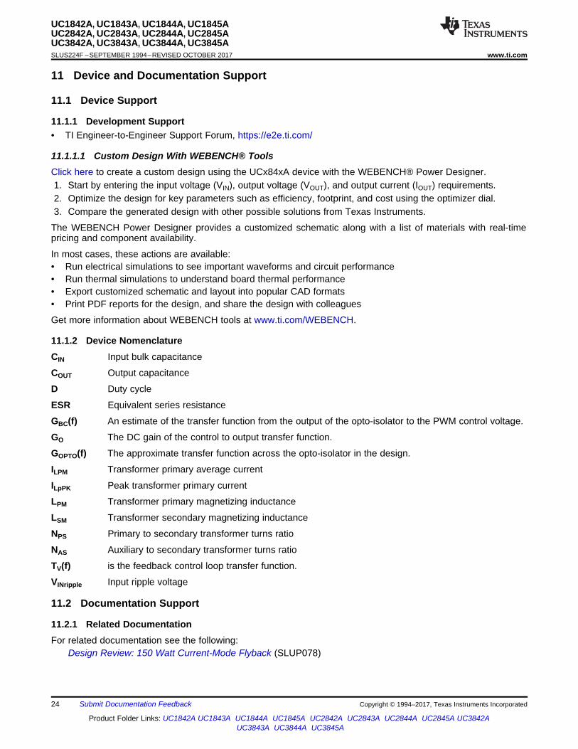
11.1 Device Support
11.1.1 Development Support• TI Engineer-to-Engineer Support Forum, https://e2e.ti.com/
11.1.1.1 Custom Design With WEBENCH® ToolsClick here to create a custom design using the UCx84xA device with the WEBENCH® Power Designer.1. Start by entering the input voltage (VIN), output voltage (VOUT), and output current (IOUT) requirements.2. Optimize the design for key parameters such as efficiency, footprint, and cost using the optimizer dial.3. Compare the generated design with other possible solutions from Texas Instruments.
The WEBENCH Power Designer provides a customized schematic along with a list of materials with real-timepricing and component availability.
In most cases, these actions are available:• Run electrical simulations to see important waveforms and circuit performance• Run thermal simulations to understand board thermal performance• Export customized schematic and layout into popular CAD formats• Print PDF reports for the design, and share the design with colleagues
Get more information about WEBENCH tools at www.ti.com/WEBENCH.
11.1.2 Device NomenclatureCIN Input bulk capacitance
COUT Output capacitance
D Duty cycle
ESR Equivalent series resistance
GBC(f) An estimate of the transfer function from the output of the opto-isolator to the PWM control voltage.
GO The DC gain of the control to output transfer function.
GOPTO(f) The approximate transfer function across the opto-isolator in the design.
ILPM Transformer primary average current
ILpPK Peak transformer primary current
LPM Transformer primary magnetizing inductance
LSM Transformer secondary magnetizing inductance
NPS Primary to secondary transformer turns ratio
NAS Auxiliary to secondary transformer turns ratio
TV(f) is the feedback control loop transfer function.
VINripple Input ripple voltage
11.2 Documentation Support
11.2.1 Related DocumentationFor related documentation see the following:
Design Review: 150 Watt Current-Mode Flyback (SLUP078)

25
UC1842A, UC1843A, UC1844A, UC1845AUC2842A, UC2843A, UC2844A, UC2845AUC3842A, UC3843A, UC3844A, UC3845A
www.ti.com SLUS224F –SEPTEMBER 1994–REVISED OCTOBER 2017
Product Folder Links: UC1842A UC1843A UC1844A UC1845A UC2842A UC2843A UC2844A UC2845A UC3842AUC3843A UC3844A UC3845A
Submit Documentation FeedbackCopyright © 1994–2017, Texas Instruments Incorporated
11.3 Related LinksThe table below lists quick access links. Categories include technical documents, support and communityresources, tools and software, and quick access to sample or buy.
Table 2. Related Links
PARTS PRODUCT FOLDER SAMPLE & BUY TECHNICALDOCUMENTS
TOOLS &SOFTWARE
SUPPORT &COMMUNITY
UC1842A Click here Click here Click here Click here Click hereUC1843A Click here Click here Click here Click here Click hereUC1844A Click here Click here Click here Click here Click hereUC1845A Click here Click here Click here Click here Click hereUC2842A Click here Click here Click here Click here Click hereUC2843A Click here Click here Click here Click here Click hereUC2844A Click here Click here Click here Click here Click hereUC2845A Click here Click here Click here Click here Click hereUC3842A Click here Click here Click here Click here Click hereUC3843A Click here Click here Click here Click here Click hereUC3844A Click here Click here Click here Click here Click hereUC3845A Click here Click here Click here Click here Click here
11.4 Receiving Notification of Documentation UpdatesTo receive notification of documentation updates, navigate to the device product folder on ti.com. In the upperright corner, click on Alert me to register and receive a weekly digest of any product information that haschanged. For change details, review the revision history included in any revised document.
11.5 Community ResourcesThe following links connect to TI community resources. Linked contents are provided "AS IS" by the respectivecontributors. They do not constitute TI specifications and do not necessarily reflect TI's views; see TI's Terms ofUse.
TI E2E™ Online Community TI's Engineer-to-Engineer (E2E) Community. Created to foster collaborationamong engineers. At e2e.ti.com, you can ask questions, share knowledge, explore ideas and helpsolve problems with fellow engineers.
Design Support TI's Design Support Quickly find helpful E2E forums along with design support tools andcontact information for technical support.
11.6 TrademarksE2E is a trademark of Texas Instruments.WEBENCH is a registered trademark of Texas Instruments.All other trademarks are the property of their respective owners.
11.7 Electrostatic Discharge CautionThis integrated circuit can be damaged by ESD. Texas Instruments recommends that all integrated circuits be handled withappropriate precautions. Failure to observe proper handling and installation procedures can cause damage.
ESD damage can range from subtle performance degradation to complete device failure. Precision integrated circuits may be moresusceptible to damage because very small parametric changes could cause the device not to meet its published specifications.
11.8 GlossarySLYZ022 — TI Glossary.
This glossary lists and explains terms, acronyms, and definitions.

26
UC1842A, UC1843A, UC1844A, UC1845AUC2842A, UC2843A, UC2844A, UC2845AUC3842A, UC3843A, UC3844A, UC3845ASLUS224F –SEPTEMBER 1994–REVISED OCTOBER 2017 www.ti.com
Product Folder Links: UC1842A UC1843A UC1844A UC1845A UC2842A UC2843A UC2844A UC2845A UC3842AUC3843A UC3844A UC3845A
Submit Documentation Feedback Copyright © 1994–2017, Texas Instruments Incorporated
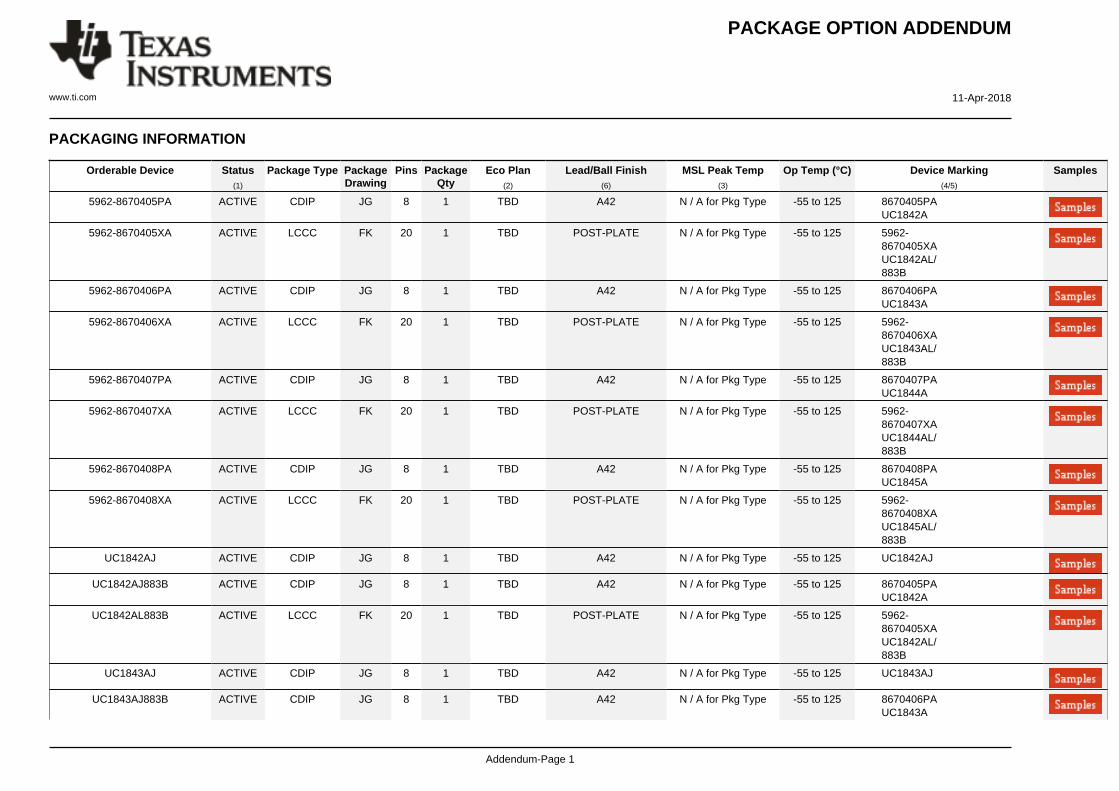
12 Mechanical, Packaging, and Orderable InformationThe following pages include mechanical, packaging, and orderable information. This information is the mostcurrent data available for the designated devices. This data is subject to change without notice and revision ofthis document. For browser-based versions of this data sheet, refer to the left-hand navigation.
PACKAGE OPTION ADDENDUM
www.ti.com 11-Apr-2018
Addendum-Page 1
PACKAGING INFORMATION
Orderable Device Status(1)
Package Type PackageDrawing
Pins PackageQty
Eco Plan(2)
Lead/Ball Finish(6)
MSL Peak Temp(3)
Op Temp (°C) Device Marking(4/5)
Samples
5962-8670405PA ACTIVE CDIP JG 8 1 TBD A42 N / A for Pkg Type -55 to 125 8670405PAUC1842A
5962-8670405XA ACTIVE LCCC FK 20 1 TBD POST-PLATE N / A for Pkg Type -55 to 125 5962-8670405XAUC1842AL/883B
5962-8670406PA ACTIVE CDIP JG 8 1 TBD A42 N / A for Pkg Type -55 to 125 8670406PAUC1843A
5962-8670406XA ACTIVE LCCC FK 20 1 TBD POST-PLATE N / A for Pkg Type -55 to 125 5962-8670406XAUC1843AL/883B
5962-8670407PA ACTIVE CDIP JG 8 1 TBD A42 N / A for Pkg Type -55 to 125 8670407PAUC1844A
5962-8670407XA ACTIVE LCCC FK 20 1 TBD POST-PLATE N / A for Pkg Type -55 to 125 5962-8670407XAUC1844AL/883B
5962-8670408PA ACTIVE CDIP JG 8 1 TBD A42 N / A for Pkg Type -55 to 125 8670408PAUC1845A
5962-8670408XA ACTIVE LCCC FK 20 1 TBD POST-PLATE N / A for Pkg Type -55 to 125 5962-8670408XAUC1845AL/883B
UC1842AJ ACTIVE CDIP JG 8 1 TBD A42 N / A for Pkg Type -55 to 125 UC1842AJ
UC1842AJ883B ACTIVE CDIP JG 8 1 TBD A42 N / A for Pkg Type -55 to 125 8670405PAUC1842A
UC1842AL883B ACTIVE LCCC FK 20 1 TBD POST-PLATE N / A for Pkg Type -55 to 125 5962-8670405XAUC1842AL/883B
UC1843AJ ACTIVE CDIP JG 8 1 TBD A42 N / A for Pkg Type -55 to 125 UC1843AJ
UC1843AJ883B ACTIVE CDIP JG 8 1 TBD A42 N / A for Pkg Type -55 to 125 8670406PAUC1843A

PACKAGE OPTION ADDENDUM
www.ti.com 11-Apr-2018
Addendum-Page 2
Orderable Device Status(1)
Package Type PackageDrawing
Pins PackageQty
Eco Plan(2)
Lead/Ball Finish(6)
MSL Peak Temp(3)
Op Temp (°C) Device Marking(4/5)
Samples
UC1843AL883B ACTIVE LCCC FK 20 1 TBD POST-PLATE N / A for Pkg Type -55 to 125 5962-8670406XAUC1843AL/883B
UC1844AJ ACTIVE CDIP JG 8 1 TBD A42 N / A for Pkg Type -55 to 125 UC1844AJ
UC1844AJ883B ACTIVE CDIP JG 8 1 TBD A42 N / A for Pkg Type -55 to 125 8670407PAUC1844A
UC1844AL883B ACTIVE LCCC FK 20 1 TBD POST-PLATE N / A for Pkg Type -55 to 125 5962-8670407XAUC1844AL/883B
UC1845AJ ACTIVE CDIP JG 8 1 TBD A42 N / A for Pkg Type -55 to 125 UC1845AJ
UC1845AJ883B ACTIVE CDIP JG 8 1 TBD A42 N / A for Pkg Type -55 to 125 8670408PAUC1845A
UC1845AL883B ACTIVE LCCC FK 20 1 TBD POST-PLATE N / A for Pkg Type -55 to 125 5962-8670408XAUC1845AL/883B
UC2842AD ACTIVE SOIC D 14 50 Green (RoHS& no Sb/Br)
CU NIPDAU Level-1-260C-UNLIM -40 to 85 UC2842AD
UC2842AD8 ACTIVE SOIC D 8 75 Green (RoHS& no Sb/Br)
CU NIPDAU Level-1-260C-UNLIM -40 to 85 UC2842AUC2842AD8
UC2842AD8G4 ACTIVE SOIC D 8 75 Green (RoHS& no Sb/Br)
CU NIPDAU Level-1-260C-UNLIM -40 to 85 UC2842AUC2842AD8
UC2842AD8TR ACTIVE SOIC D 8 2500 Green (RoHS& no Sb/Br)
CU NIPDAU Level-1-260C-UNLIM -40 to 85 UC2842AUC2842AD8
UC2842AD8TRG4 ACTIVE SOIC D 8 2500 Green (RoHS& no Sb/Br)
CU NIPDAU Level-1-260C-UNLIM -40 to 85 UC2842AUC2842AD8
UC2842ADG4 ACTIVE SOIC D 14 50 Green (RoHS& no Sb/Br)
CU NIPDAU Level-1-260C-UNLIM -40 to 85 UC2842AD
UC2842ADTR ACTIVE SOIC D 14 2500 Green (RoHS& no Sb/Br)
CU NIPDAU Level-1-260C-UNLIM -40 to 85 UC2842AD

PACKAGE OPTION ADDENDUM
www.ti.com 11-Apr-2018
Addendum-Page 3
Orderable Device Status(1)
Package Type PackageDrawing
Pins PackageQty
Eco Plan(2)
Lead/Ball Finish(6)
MSL Peak Temp(3)
Op Temp (°C) Device Marking(4/5)
Samples
UC2842ADW ACTIVE SOIC DW 16 40 Green (RoHS& no Sb/Br)
CU NIPDAU Level-2-260C-1 YEAR -40 to 85 UC2842ADW
UC2842ADWTR ACTIVE SOIC DW 16 2000 Green (RoHS& no Sb/Br)
CU NIPDAU Level-2-260C-1 YEAR -40 to 85 UC2842ADW
UC2842ADWTRG4 ACTIVE SOIC DW 16 2000 Green (RoHS& no Sb/Br)
CU NIPDAU Level-2-260C-1 YEAR -40 to 85 UC2842ADW
UC2842AN ACTIVE PDIP P 8 50 Green (RoHS& no Sb/Br)
CU NIPDAU | Call TI N / A for Pkg Type -40 to 85 UC2842AN
UC2842ANG4 ACTIVE PDIP P 8 50 Green (RoHS& no Sb/Br)
Call TI N / A for Pkg Type -40 to 85 UC2842AN
UC2843AD ACTIVE SOIC D 14 50 Green (RoHS& no Sb/Br)
CU NIPDAU Level-1-260C-UNLIM -40 to 85 UC2843AD
UC2843AD8 ACTIVE SOIC D 8 75 Green (RoHS& no Sb/Br)
CU NIPDAU Level-1-260C-UNLIM -40 to 85 UC2843AUC2843AD8
UC2843AD8G4 ACTIVE SOIC D 8 75 Green (RoHS& no Sb/Br)
CU NIPDAU Level-1-260C-UNLIM -40 to 85 UC2843AUC2843AD8
UC2843AD8TR ACTIVE SOIC D 8 2500 Green (RoHS& no Sb/Br)
CU NIPDAU Level-1-260C-UNLIM -40 to 85 UC2843AUC2843AD8
UC2843AD8TRG4 ACTIVE SOIC D 8 2500 Green (RoHS& no Sb/Br)
CU NIPDAU Level-1-260C-UNLIM -40 to 85 UC2843AUC2843AD8
UC2843ADG4 ACTIVE SOIC D 14 50 Green (RoHS& no Sb/Br)
CU NIPDAU Level-1-260C-UNLIM -40 to 85 UC2843AD
UC2843ADTR ACTIVE SOIC D 14 2500 Green (RoHS& no Sb/Br)
CU NIPDAU Level-1-260C-UNLIM -40 to 85 UC2843AD
UC2843AN ACTIVE PDIP P 8 50 Green (RoHS& no Sb/Br)
CU NIPDAU | Call TI N / A for Pkg Type -40 to 85 UC2843AN
UC2843ANG4 ACTIVE PDIP P 8 50 Green (RoHS& no Sb/Br)
Call TI N / A for Pkg Type -40 to 85 UC2843AN
UC2843AQ NRND PLCC FN 20 46 Green (RoHS& no Sb/Br)
CU SN Level-2-260C-1 YEAR -40 to 85 UC2843AQ
UC2844AD ACTIVE SOIC D 14 50 Green (RoHS& no Sb/Br)
CU NIPDAU Level-1-260C-UNLIM -40 to 85 UC2844AD

PACKAGE OPTION ADDENDUM
www.ti.com 11-Apr-2018
Addendum-Page 4
Orderable Device Status(1)
Package Type PackageDrawing
Pins PackageQty
Eco Plan(2)
Lead/Ball Finish(6)
MSL Peak Temp(3)
Op Temp (°C) Device Marking(4/5)
Samples
UC2844AD8 ACTIVE SOIC D 8 75 Green (RoHS& no Sb/Br)
CU NIPDAU Level-1-260C-UNLIM -40 to 85 UC2844AUC2844AD8
UC2844AD8G4 ACTIVE SOIC D 8 75 Green (RoHS& no Sb/Br)
CU NIPDAU Level-1-260C-UNLIM -40 to 85 UC2844AUC2844AD8
UC2844AD8TR ACTIVE SOIC D 8 2500 Green (RoHS& no Sb/Br)
CU NIPDAU Level-1-260C-UNLIM -40 to 85 UC2844AUC2844AD8
UC2844AD8TRG4 ACTIVE SOIC D 8 2500 Green (RoHS& no Sb/Br)
CU NIPDAU Level-1-260C-UNLIM -40 to 85 UC2844AUC2844AD8
UC2844ADG4 ACTIVE SOIC D 14 50 Green (RoHS& no Sb/Br)
CU NIPDAU Level-1-260C-UNLIM -40 to 85 UC2844AD
UC2844ADTR ACTIVE SOIC D 14 2500 Green (RoHS& no Sb/Br)
CU NIPDAU Level-1-260C-UNLIM -40 to 85 UC2844AD
UC2844ADTRG4 ACTIVE SOIC D 14 2500 Green (RoHS& no Sb/Br)
CU NIPDAU Level-1-260C-UNLIM -40 to 85 UC2844AD
UC2844AN ACTIVE PDIP P 8 50 Green (RoHS& no Sb/Br)
CU NIPDAU | Call TI N / A for Pkg Type -40 to 85 UC2844AN
UC2844ANG4 ACTIVE PDIP P 8 50 Green (RoHS& no Sb/Br)
Call TI N / A for Pkg Type -40 to 85 UC2844AN
UC2844AQD8 ACTIVE SOIC D 8 75 Green (RoHS& no Sb/Br)
CU NIPDAU Level-1-260C-UNLIM -40 to 125 (2844AQ, UC2844AQ)
UC2844AQD8R ACTIVE SOIC D 8 2500 Green (RoHS& no Sb/Br)
CU NIPDAU Level-1-260C-UNLIM -40 to 125 (2844AQ, UC2844AQ)
UC2844AQDR ACTIVE SOIC D 14 2500 Green (RoHS& no Sb/Br)
CU NIPDAU Level-1-260C-UNLIM -40 to 125 (2844AQ, UC2844AQ)
UC2845AD ACTIVE SOIC D 14 50 Green (RoHS& no Sb/Br)
CU NIPDAU Level-1-260C-UNLIM -40 to 85 UC2845AD
UC2845AD8 ACTIVE SOIC D 8 75 Green (RoHS& no Sb/Br)
CU NIPDAU Level-1-260C-UNLIM -40 to 85 UC2845AUC2845AD8
UC2845AD8G4 ACTIVE SOIC D 8 75 Green (RoHS& no Sb/Br)
CU NIPDAU Level-1-260C-UNLIM -40 to 85 UC2845AUC2845AD8

PACKAGE OPTION ADDENDUM
www.ti.com 11-Apr-2018
Addendum-Page 5
Orderable Device Status(1)
Package Type PackageDrawing
Pins PackageQty
Eco Plan(2)
Lead/Ball Finish(6)
MSL Peak Temp(3)
Op Temp (°C) Device Marking(4/5)
Samples
UC2845AD8TR ACTIVE SOIC D 8 2500 Green (RoHS& no Sb/Br)
CU NIPDAU Level-1-260C-UNLIM -40 to 85 UC2845AUC2845AD8
UC2845AD8TRG4 ACTIVE SOIC D 8 2500 Green (RoHS& no Sb/Br)
CU NIPDAU Level-1-260C-UNLIM -40 to 85 UC2845AUC2845AD8
UC2845ADG4 ACTIVE SOIC D 14 50 Green (RoHS& no Sb/Br)
CU NIPDAU Level-1-260C-UNLIM -40 to 85 UC2845AD
UC2845ADTR ACTIVE SOIC D 14 2500 Green (RoHS& no Sb/Br)
CU NIPDAU Level-1-260C-UNLIM -40 to 85 UC2845AD
UC2845ADTRG4 ACTIVE SOIC D 14 2500 Green (RoHS& no Sb/Br)
CU NIPDAU Level-1-260C-UNLIM -40 to 85 UC2845AD
UC2845ADW ACTIVE SOIC DW 16 40 Green (RoHS& no Sb/Br)
CU NIPDAU Level-2-260C-1 YEAR -40 to 85 UC2845ADW
UC2845AN ACTIVE PDIP P 8 50 Green (RoHS& no Sb/Br)
CU NIPDAU | Call TI N / A for Pkg Type -40 to 85 UC2845AN
UC2845ANG4 ACTIVE PDIP P 8 50 Green (RoHS& no Sb/Br)
Call TI N / A for Pkg Type -40 to 85 UC2845AN
UC3842AD ACTIVE SOIC D 14 50 Green (RoHS& no Sb/Br)
CU NIPDAU Level-1-260C-UNLIM 0 to 70 UC3842AD
UC3842AD8 ACTIVE SOIC D 8 75 Green (RoHS& no Sb/Br)
CU NIPDAU Level-1-260C-UNLIM 0 to 70 UC3842AUC3842AD8
UC3842AD8G4 ACTIVE SOIC D 8 75 Green (RoHS& no Sb/Br)
CU NIPDAU Level-1-260C-UNLIM 0 to 70 UC3842AUC3842AD8
UC3842AD8TR ACTIVE SOIC D 8 2500 Green (RoHS& no Sb/Br)
CU NIPDAU Level-1-260C-UNLIM 0 to 70 UC3842AUC3842AD8
UC3842AD8TRG4 ACTIVE SOIC D 8 2500 Green (RoHS& no Sb/Br)
CU NIPDAU Level-1-260C-UNLIM 0 to 70 UC3842AUC3842AD8
UC3842ADG4 ACTIVE SOIC D 14 50 Green (RoHS& no Sb/Br)
CU NIPDAU Level-1-260C-UNLIM 0 to 70 UC3842AD
UC3842ADTR ACTIVE SOIC D 14 2500 Green (RoHS& no Sb/Br)
CU NIPDAU Level-1-260C-UNLIM 0 to 70 UC3842AD

PACKAGE OPTION ADDENDUM
www.ti.com 11-Apr-2018
Addendum-Page 6
Orderable Device Status(1)
Package Type PackageDrawing
Pins PackageQty
Eco Plan(2)
Lead/Ball Finish(6)
MSL Peak Temp(3)
Op Temp (°C) Device Marking(4/5)
Samples
UC3842ADW ACTIVE SOIC DW 16 40 Green (RoHS& no Sb/Br)
CU NIPDAU Level-2-260C-1 YEAR 0 to 70 UC3842ADW
UC3842ADWG4 ACTIVE SOIC DW 16 40 Green (RoHS& no Sb/Br)
CU NIPDAU Level-2-260C-1 YEAR 0 to 70 UC3842ADW
UC3842AN ACTIVE PDIP P 8 50 Green (RoHS& no Sb/Br)
CU NIPDAU | Call TI N / A for Pkg Type 0 to 70 UC3842AN
UC3842ANG4 ACTIVE PDIP P 8 50 Green (RoHS& no Sb/Br)
Call TI N / A for Pkg Type 0 to 70 UC3842AN
UC3842J ACTIVE CDIP JG 8 1 TBD A42 N / A for Pkg Type -40 to 85 UC3842J
UC3843AD ACTIVE SOIC D 14 50 Green (RoHS& no Sb/Br)
CU NIPDAU Level-1-260C-UNLIM 0 to 70 UC3843AD
UC3843AD8 ACTIVE SOIC D 8 75 Green (RoHS& no Sb/Br)
CU NIPDAU Level-1-260C-UNLIM 0 to 70 UC3843AUC3843AD8
UC3843AD8G4 ACTIVE SOIC D 8 75 Green (RoHS& no Sb/Br)
CU NIPDAU Level-1-260C-UNLIM 0 to 70 UC3843AUC3843AD8
UC3843AD8TR ACTIVE SOIC D 8 2500 Green (RoHS& no Sb/Br)
CU NIPDAU Level-1-260C-UNLIM 0 to 70 UC3843AUC3843AD8
UC3843AD8TRG4 ACTIVE SOIC D 8 2500 Green (RoHS& no Sb/Br)
CU NIPDAU Level-1-260C-UNLIM 0 to 70 UC3843AUC3843AD8
UC3843ADG4 ACTIVE SOIC D 14 50 Green (RoHS& no Sb/Br)
CU NIPDAU Level-1-260C-UNLIM 0 to 70 UC3843AD
UC3843ADTR ACTIVE SOIC D 14 2500 Green (RoHS& no Sb/Br)
CU NIPDAU Level-1-260C-UNLIM 0 to 70 UC3843AD
UC3843ADTRG4 ACTIVE SOIC D 14 2500 Green (RoHS& no Sb/Br)
CU NIPDAU Level-1-260C-UNLIM 0 to 70 UC3843AD
UC3843AN ACTIVE PDIP P 8 50 Green (RoHS& no Sb/Br)
CU NIPDAU | Call TI N / A for Pkg Type 0 to 70 UC3843AN
UC3843ANG4 ACTIVE PDIP P 8 50 Green (RoHS& no Sb/Br)
Call TI N / A for Pkg Type 0 to 70 UC3843AN
UC3844AD ACTIVE SOIC D 14 50 Green (RoHS& no Sb/Br)
CU NIPDAU Level-1-260C-UNLIM 0 to 70 UC3844AD

PACKAGE OPTION ADDENDUM
www.ti.com 11-Apr-2018
Addendum-Page 7
Orderable Device Status(1)
Package Type PackageDrawing
Pins PackageQty
Eco Plan(2)
Lead/Ball Finish(6)
MSL Peak Temp(3)
Op Temp (°C) Device Marking(4/5)
Samples
UC3844AD8 ACTIVE SOIC D 8 75 Green (RoHS& no Sb/Br)
CU NIPDAU Level-1-260C-UNLIM 0 to 70 UC3844AUC3844AD8
UC3844AD8G4 ACTIVE SOIC D 8 75 Green (RoHS& no Sb/Br)
CU NIPDAU Level-1-260C-UNLIM 0 to 70 UC3844AUC3844AD8
UC3844AD8TR ACTIVE SOIC D 8 2500 Green (RoHS& no Sb/Br)
CU NIPDAU Level-1-260C-UNLIM 0 to 70 UC3844AUC3844AD8
UC3844AD8TRG4 ACTIVE SOIC D 8 2500 Green (RoHS& no Sb/Br)
CU NIPDAU Level-1-260C-UNLIM 0 to 70 UC3844AUC3844AD8
UC3844ADG4 ACTIVE SOIC D 14 50 Green (RoHS& no Sb/Br)
CU NIPDAU Level-1-260C-UNLIM 0 to 70 UC3844AD
UC3844ADTR ACTIVE SOIC D 14 2500 Green (RoHS& no Sb/Br)
CU NIPDAU Level-1-260C-UNLIM 0 to 70 UC3844AD
UC3844ADTRG4 ACTIVE SOIC D 14 2500 Green (RoHS& no Sb/Br)
CU NIPDAU Level-1-260C-UNLIM 0 to 70 UC3844AD
UC3844AN ACTIVE PDIP P 8 50 Green (RoHS& no Sb/Br)
CU NIPDAU | Call TI N / A for Pkg Type 0 to 70 UC3844AN
UC3844ANG4 ACTIVE PDIP P 8 50 Green (RoHS& no Sb/Br)
Call TI N / A for Pkg Type 0 to 70 UC3844AN
UC3845AD ACTIVE SOIC D 14 50 Green (RoHS& no Sb/Br)
CU NIPDAU Level-1-260C-UNLIM 0 to 70 UC3845AD
UC3845AD8 ACTIVE SOIC D 8 75 Green (RoHS& no Sb/Br)
CU NIPDAU Level-1-260C-UNLIM 0 to 70 UC3845AUC3845AD8
UC3845AD8G4 ACTIVE SOIC D 8 75 Green (RoHS& no Sb/Br)
CU NIPDAU Level-1-260C-UNLIM 0 to 70 UC3845AUC3845AD8
UC3845AD8TR ACTIVE SOIC D 8 2500 Green (RoHS& no Sb/Br)
CU NIPDAU Level-1-260C-UNLIM 0 to 70 UC3845AUC3845AD8
UC3845AD8TRG4 ACTIVE SOIC D 8 2500 Green (RoHS& no Sb/Br)
CU NIPDAU Level-1-260C-UNLIM 0 to 70 UC3845AUC3845AD8

PACKAGE OPTION ADDENDUM
www.ti.com 11-Apr-2018
Addendum-Page 8
Orderable Device Status(1)
Package Type PackageDrawing
Pins PackageQty
Eco Plan(2)
Lead/Ball Finish(6)
MSL Peak Temp(3)
Op Temp (°C) Device Marking(4/5)
Samples
UC3845ADG4 ACTIVE SOIC D 14 50 Green (RoHS& no Sb/Br)
CU NIPDAU Level-1-260C-UNLIM 0 to 70 UC3845AD
UC3845ADTR ACTIVE SOIC D 14 2500 Green (RoHS& no Sb/Br)
CU NIPDAU Level-1-260C-UNLIM 0 to 70 UC3845AD
UC3845ADTRG4 ACTIVE SOIC D 14 2500 Green (RoHS& no Sb/Br)
CU NIPDAU Level-1-260C-UNLIM 0 to 70 UC3845AD
UC3845AN ACTIVE PDIP P 8 50 Green (RoHS& no Sb/Br)
CU NIPDAU | Call TI N / A for Pkg Type 0 to 70 UC3845AN
UC3845ANG4 ACTIVE PDIP P 8 50 Green (RoHS& no Sb/Br)
Call TI N / A for Pkg Type 0 to 70 UC3845AN
(1) The marketing status values are defined as follows:ACTIVE: Product device recommended for new designs.LIFEBUY: TI has announced that the device will be discontinued, and a lifetime-buy period is in effect.NRND: Not recommended for new designs. Device is in production to support existing customers, but TI does not recommend using this part in a new design.PREVIEW: Device has been announced but is not in production. Samples may or may not be available.OBSOLETE: TI has discontinued the production of the device.
(2) RoHS: TI defines "RoHS" to mean semiconductor products that are compliant with the current EU RoHS requirements for all 10 RoHS substances, including the requirement that RoHS substancedo not exceed 0.1% by weight in homogeneous materials. Where designed to be soldered at high temperatures, "RoHS" products are suitable for use in specified lead-free processes. TI mayreference these types of products as "Pb-Free".RoHS Exempt: TI defines "RoHS Exempt" to mean products that contain lead but are compliant with EU RoHS pursuant to a specific EU RoHS exemption.Green: TI defines "Green" to mean the content of Chlorine (Cl) and Bromine (Br) based flame retardants meet JS709B low halogen requirements of <=1000ppm threshold. Antimony trioxide basedflame retardants must also meet the <=1000ppm threshold requirement.
(3) MSL, Peak Temp. - The Moisture Sensitivity Level rating according to the JEDEC industry standard classifications, and peak solder temperature.
(4) There may be additional marking, which relates to the logo, the lot trace code information, or the environmental category on the device.
(5) Multiple Device Markings will be inside parentheses. Only one Device Marking contained in parentheses and separated by a "~" will appear on a device. If a line is indented then it is a continuationof the previous line and the two combined represent the entire Device Marking for that device.
(6) Lead/Ball Finish - Orderable Devices may have multiple material finish options. Finish options are separated by a vertical ruled line. Lead/Ball Finish values may wrap to two lines if the finishvalue exceeds the maximum column width.
Important Information and Disclaimer:The information provided on this page represents TI's knowledge and belief as of the date that it is provided. TI bases its knowledge and belief on informationprovided by third parties, and makes no representation or warranty as to the accuracy of such information. Efforts are underway to better integrate information from third parties. TI has taken and

PACKAGE OPTION ADDENDUM
www.ti.com 11-Apr-2018
Addendum-Page 9
continues to take reasonable steps to provide representative and accurate information but may not have conducted destructive testing or chemical analysis on incoming materials and chemicals.TI and TI suppliers consider certain information to be proprietary, and thus CAS numbers and other limited information may not be available for release.
In no event shall TI's liability arising out of such information exceed the total purchase price of the TI part(s) at issue in this document sold by TI to Customer on an annual basis.
OTHER QUALIFIED VERSIONS OF UC1842A, UC1843A, UC1844A, UC1845A, UC2843A, UC3842A, UC3842M, UC3843A, UC3844A, UC3845A :
• Catalog: UC3842A, UC3843A, UC3844A, UC3845A, UC3842, UC3845AM
• Automotive: UC2843A-Q1
• Enhanced Product: UC1842A-EP, UC1843A-EP, UC1844A-EP, UC1845A-EP, UC1842A-EP, UC1843A-EP, UC1844A-EP, UC1845A-EP
• Military: UC1842A, UC1843A, UC1844A, UC1845A
• Space: UC1842A-SP, UC1843A-SP, UC1844A-SP, UC1845A-SP, UC1842A-SP, UC1843A-SP, UC1844A-SP, UC1845A-SP
NOTE: Qualified Version Definitions:
• Catalog - TI's standard catalog product
• Automotive - Q100 devices qualified for high-reliability automotive applications targeting zero defects
• Enhanced Product - Supports Defense, Aerospace and Medical Applications
• Military - QML certified for Military and Defense Applications
• Space - Radiation tolerant, ceramic packaging and qualified for use in Space-based application

TAPE AND REEL INFORMATION
*All dimensions are nominal
Device PackageType
PackageDrawing
Pins SPQ ReelDiameter
(mm)
ReelWidth
W1 (mm)
A0(mm)
B0(mm)
K0(mm)
P1(mm)
W(mm)
Pin1Quadrant
UC2842AD8TR SOIC D 8 2500 330.0 12.4 6.4 5.2 2.1 8.0 12.0 Q1
UC2842ADTR SOIC D 14 2500 330.0 16.4 6.5 9.0 2.1 8.0 16.0 Q1
UC2842ADWTR SOIC DW 16 2000 330.0 16.4 10.75 10.7 2.7 12.0 16.0 Q1
UC2843AD8TR SOIC D 8 2500 330.0 12.4 6.4 5.2 2.1 8.0 12.0 Q1
UC2843ADTR SOIC D 14 2500 330.0 16.4 6.5 9.0 2.1 8.0 16.0 Q1
UC2844AD8TR SOIC D 8 2500 330.0 12.4 6.4 5.2 2.1 8.0 12.0 Q1
UC2844ADTR SOIC D 14 2500 330.0 16.4 6.5 9.0 2.1 8.0 16.0 Q1
UC2844AQD8R SOIC D 8 2500 330.0 12.4 6.4 5.2 2.1 8.0 12.0 Q1
UC2844AQDR SOIC D 14 2500 330.0 16.4 6.5 9.0 2.1 8.0 16.0 Q1
UC2845AD8TR SOIC D 8 2500 330.0 12.4 6.4 5.2 2.1 8.0 12.0 Q1
UC2845ADTR SOIC D 14 2500 330.0 16.4 6.5 9.0 2.1 8.0 16.0 Q1
UC3842AD8TR SOIC D 8 2500 330.0 12.4 6.4 5.2 2.1 8.0 12.0 Q1
UC3842ADTR SOIC D 14 2500 330.0 16.4 6.5 9.0 2.1 8.0 16.0 Q1
UC3843AD8TR SOIC D 8 2500 330.0 12.4 6.4 5.2 2.1 8.0 12.0 Q1
UC3843ADTR SOIC D 14 2500 330.0 16.4 6.5 9.0 2.1 8.0 16.0 Q1
UC3844AD8TR SOIC D 8 2500 330.0 12.4 6.4 5.2 2.1 8.0 12.0 Q1
UC3844ADTR SOIC D 14 2500 330.0 16.4 6.5 9.0 2.1 8.0 16.0 Q1
UC3845AD8TR SOIC D 8 2500 330.0 12.4 6.4 5.2 2.1 8.0 12.0 Q1
PACKAGE MATERIALS INFORMATION
www.ti.com 6-Jan-2017
Pack Materials-Page 1

Device PackageType
PackageDrawing
Pins SPQ ReelDiameter
(mm)
ReelWidth
W1 (mm)
A0(mm)
B0(mm)
K0(mm)
P1(mm)
W(mm)
Pin1Quadrant
UC3845ADTR SOIC D 14 2500 330.0 16.4 6.5 9.0 2.1 8.0 16.0 Q1
*All dimensions are nominal
Device Package Type Package Drawing Pins SPQ Length (mm) Width (mm) Height (mm)
UC2842AD8TR SOIC D 8 2500 340.5 338.1 20.6
UC2842ADTR SOIC D 14 2500 333.2 345.9 28.6
UC2842ADWTR SOIC DW 16 2000 367.0 367.0 38.0
UC2843AD8TR SOIC D 8 2500 340.5 338.1 20.6
UC2843ADTR SOIC D 14 2500 333.2 345.9 28.6
UC2844AD8TR SOIC D 8 2500 340.5 338.1 20.6
UC2844ADTR SOIC D 14 2500 333.2 345.9 28.6
UC2844AQD8R SOIC D 8 2500 367.0 367.0 35.0
UC2844AQDR SOIC D 14 2500 367.0 367.0 38.0
UC2845AD8TR SOIC D 8 2500 340.5 338.1 20.6
UC2845ADTR SOIC D 14 2500 333.2 345.9 28.6
UC3842AD8TR SOIC D 8 2500 340.5 338.1 20.6
UC3842ADTR SOIC D 14 2500 333.2 345.9 28.6
UC3843AD8TR SOIC D 8 2500 340.5 338.1 20.6
UC3843ADTR SOIC D 14 2500 333.2 345.9 28.6
UC3844AD8TR SOIC D 8 2500 340.5 338.1 20.6
PACKAGE MATERIALS INFORMATION
www.ti.com 6-Jan-2017
Pack Materials-Page 2

Device Package Type Package Drawing Pins SPQ Length (mm) Width (mm) Height (mm)
UC3844ADTR SOIC D 14 2500 333.2 345.9 28.6
UC3845AD8TR SOIC D 8 2500 340.5 338.1 20.6
UC3845ADTR SOIC D 14 2500 333.2 345.9 28.6
PACKAGE MATERIALS INFORMATION
www.ti.com 6-Jan-2017
Pack Materials-Page 3


www.ti.com
PACKAGE OUTLINE
C
20X -.021.013-0.530.33[ ]
20X -.032.026-0.810.66[ ]
TYP
-.395.385-10.039.78[ ]
16X .050[1.27]
-.339.283-8.617.19[ ]
(.008)[0.2]
TYP-.120.090-3.042.29[ ]
.180 MAX[4.57]
.020 MIN[0.51]
B
NOTE 3
-.356.350-9.048.89[ ]
A
NOTE 3
-.356.350-9.048.89[ ]
4215152/B 04/2017
4215152/B 04/2017
PLCC - 4.57 mm max heightFN0020APLASTIC CHIP CARRIER
NOTES: 1. All linear dimensions are in inches. Any dimensions in brackets are in millimeters. Any dimensions in parenthesis are for reference only. Controlling dimensions are in inches. Dimensioning and tolerancing per ASME Y14.5M. 2. This drawing is subject to change without notice.3. Dimension does not include mold protrusion. Maximum allowable mold protrusion .01 in [0.25 mm] per side.4. Reference JEDEC registration MS-018.
PIN 1 ID(OPTIONAL)
1 203
9 13
14
184
8
.004 [0.1] C
.007 [0.18] C A B
SEATING PLANE
SCALE 1.300

www.ti.com
EXAMPLE BOARD LAYOUT
.002 MAX[0.05]
ALL AROUND
.002 MIN[0.05]
ALL AROUND
20X (.096 )[2.45]
20X (.025 )[0.64]
16X (.050 )[1.27]
(.327)[8.3]
(.327)[8.3]
(R.002 ) TYP[0.05]
4215152/B 04/2017
4215152/B 04/2017
PLCC - 4.57 mm max heightFN0020APLASTIC CHIP CARRIER
NOTES: (continued) 5. Publication IPC-7351 may have alternate designs.6. Solder mask tolerances between and around signal pads can vary based on board fabrication site.
LAND PATTERN EXAMPLEEXPOSED METAL SHOWN
SCALE:6X
SYMM
SYMM
1 203
9 13
14
184
8
METAL SOLDER MASKOPENING
NON SOLDER MASKDEFINED
(PREFERRED)SOLDER MASK DETAILS
EXPOSED METAL
SOLDER MASKOPENING
METAL UNDERSOLDER MASK
SOLDER MASKDEFINED
EXPOSED METAL

www.ti.com
EXAMPLE STENCIL DESIGN
20X (.025 )[0.64]
20X (.096 )[2.45]
(.327)[8.3]
(.327)[8.3]
16X (.050 )[1.27]
(R.002 ) TYP[0.05]
PLCC - 4.57 mm max heightFN0020APLASTIC CHIP CARRIER
4215152/B 04/2017
PLCC - 4.57 mm max heightFN0020APLASTIC CHIP CARRIER
NOTES: (continued) 7. Laser cutting apertures with trapezoidal walls and rounded corners may offer better paste release. IPC-7525 may have alternate design recommendations.8. Board assembly site may have different recommendations for stencil design.
SOLDER PASTE EXAMPLEBASED ON 0.125 mm THICK STENCIL
SCALE:6X
SYMM
SYMM
1 203
9 13
14
184
8


GENERIC PACKAGE VIEW
Images above are just a representation of the package family, actual package may vary.Refer to the product data sheet for package details.
DW 16 SOIC - 2.65 mm max heightSMALL OUTLINE INTEGRATED CIRCUIT
4040000-2/H

www.ti.com
PACKAGE OUTLINE
C
TYP10.639.97
2.65 MAX
14X 1.27
16X 0.510.31
2X8.89
TYP0.330.10
0 - 80.30.1
(1.4)
0.25GAGE PLANE
1.270.40
A
NOTE 3
10.510.1
BNOTE 4
7.67.4
4220721/A 07/2016
SOIC - 2.65 mm max heightDW0016ASOIC
NOTES: 1. All linear dimensions are in millimeters. Dimensions in parenthesis are for reference only. Dimensioning and tolerancing per ASME Y14.5M. 2. This drawing is subject to change without notice. 3. This dimension does not include mold flash, protrusions, or gate burrs. Mold flash, protrusions, or gate burrs shall not exceed 0.15 mm, per side. 4. This dimension does not include interlead flash. Interlead flash shall not exceed 0.25 mm, per side.5. Reference JEDEC registration MS-013.
1 16
0.25 C A B
98
PIN 1 IDAREA
SEATING PLANE
0.1 C
SEE DETAIL A
DETAIL ATYPICAL
SCALE 1.500

www.ti.com
EXAMPLE BOARD LAYOUT
0.07 MAXALL AROUND
0.07 MINALL AROUND
(9.3)
14X (1.27)
R0.05 TYP
16X (2)
16X (0.6)
4220721/A 07/2016
SOIC - 2.65 mm max heightDW0016ASOIC
NOTES: (continued) 6. Publication IPC-7351 may have alternate designs. 7. Solder mask tolerances between and around signal pads can vary based on board fabrication site.
METAL SOLDER MASKOPENING
NON SOLDER MASKDEFINED
SOLDER MASK DETAILS
OPENINGSOLDER MASK METAL
SOLDER MASKDEFINED
LAND PATTERN EXAMPLESCALE:7X
SYMM
1
8 9
16
SEEDETAILS
SYMM

www.ti.com
EXAMPLE STENCIL DESIGN
R0.05 TYP
16X (2)
16X (0.6)
14X (1.27)
(9.3)
4220721/A 07/2016
SOIC - 2.65 mm max heightDW0016ASOIC
NOTES: (continued) 8. Laser cutting apertures with trapezoidal walls and rounded corners may offer better paste release. IPC-7525 may have alternate design recommendations. 9. Board assembly site may have different recommendations for stencil design.
SOLDER PASTE EXAMPLEBASED ON 0.125 mm THICK STENCIL
SCALE:7X
SYMM
SYMM
1
8 9
16

MECHANICAL DATA
MCER001A – JANUARY 1995 – REVISED JANUARY 1997
POST OFFICE BOX 655303 • DALLAS, TEXAS 75265
JG (R-GDIP-T8) CERAMIC DUAL-IN-LINE
0.310 (7,87)0.290 (7,37)
0.014 (0,36)0.008 (0,20)
Seating Plane
4040107/C 08/96
5
40.065 (1,65)0.045 (1,14)
8
1
0.020 (0,51) MIN
0.400 (10,16)0.355 (9,00)
0.015 (0,38)0.023 (0,58)
0.063 (1,60)0.015 (0,38)
0.200 (5,08) MAX
0.130 (3,30) MIN
0.245 (6,22)0.280 (7,11)
0.100 (2,54)
0°–15°
NOTES: A. All linear dimensions are in inches (millimeters).B. This drawing is subject to change without notice.C. This package can be hermetically sealed with a ceramic lid using glass frit.D. Index point is provided on cap for terminal identification.E. Falls within MIL STD 1835 GDIP1-T8


IMPORTANT NOTICE
Texas Instruments Incorporated (TI) reserves the right to make corrections, enhancements, improvements and other changes to itssemiconductor products and services per JESD46, latest issue, and to discontinue any product or service per JESD48, latest issue. Buyersshould obtain the latest relevant information before placing orders and should verify that such information is current and complete.TI’s published terms of sale for semiconductor products (http://www.ti.com/sc/docs/stdterms.htm) apply to the sale of packaged integratedcircuit products that TI has qualified and released to market. Additional terms may apply to the use or sale of other types of TI products andservices.Reproduction of significant portions of TI information in TI data sheets is permissible only if reproduction is without alteration and isaccompanied by all associated warranties, conditions, limitations, and notices. TI is not responsible or liable for such reproduceddocumentation. Information of third parties may be subject to additional restrictions. Resale of TI products or services with statementsdifferent from or beyond the parameters stated by TI for that product or service voids all express and any implied warranties for theassociated TI product or service and is an unfair and deceptive business practice. TI is not responsible or liable for any such statements.Buyers and others who are developing systems that incorporate TI products (collectively, “Designers”) understand and agree that Designersremain responsible for using their independent analysis, evaluation and judgment in designing their applications and that Designers havefull and exclusive responsibility to assure the safety of Designers' applications and compliance of their applications (and of all TI productsused in or for Designers’ applications) with all applicable regulations, laws and other applicable requirements. Designer represents that, withrespect to their applications, Designer has all the necessary expertise to create and implement safeguards that (1) anticipate dangerousconsequences of failures, (2) monitor failures and their consequences, and (3) lessen the likelihood of failures that might cause harm andtake appropriate actions. Designer agrees that prior to using or distributing any applications that include TI products, Designer willthoroughly test such applications and the functionality of such TI products as used in such applications.TI’s provision of technical, application or other design advice, quality characterization, reliability data or other services or information,including, but not limited to, reference designs and materials relating to evaluation modules, (collectively, “TI Resources”) are intended toassist designers who are developing applications that incorporate TI products; by downloading, accessing or using TI Resources in anyway, Designer (individually or, if Designer is acting on behalf of a company, Designer’s company) agrees to use any particular TI Resourcesolely for this purpose and subject to the terms of this Notice.TI’s provision of TI Resources does not expand or otherwise alter TI’s applicable published warranties or warranty disclaimers for TIproducts, and no additional obligations or liabilities arise from TI providing such TI Resources. TI reserves the right to make corrections,enhancements, improvements and other changes to its TI Resources. TI has not conducted any testing other than that specificallydescribed in the published documentation for a particular TI Resource.Designer is authorized to use, copy and modify any individual TI Resource only in connection with the development of applications thatinclude the TI product(s) identified in such TI Resource. NO OTHER LICENSE, EXPRESS OR IMPLIED, BY ESTOPPEL OR OTHERWISETO ANY OTHER TI INTELLECTUAL PROPERTY RIGHT, AND NO LICENSE TO ANY TECHNOLOGY OR INTELLECTUAL PROPERTYRIGHT OF TI OR ANY THIRD PARTY IS GRANTED HEREIN, including but not limited to any patent right, copyright, mask work right, orother intellectual property right relating to any combination, machine, or process in which TI products or services are used. Informationregarding or referencing third-party products or services does not constitute a license to use such products or services, or a warranty orendorsement thereof. Use of TI Resources may require a license from a third party under the patents or other intellectual property of thethird party, or a license from TI under the patents or other intellectual property of TI.TI RESOURCES ARE PROVIDED “AS IS” AND WITH ALL FAULTS. TI DISCLAIMS ALL OTHER WARRANTIES ORREPRESENTATIONS, EXPRESS OR IMPLIED, REGARDING RESOURCES OR USE THEREOF, INCLUDING BUT NOT LIMITED TOACCURACY OR COMPLETENESS, TITLE, ANY EPIDEMIC FAILURE WARRANTY AND ANY IMPLIED WARRANTIES OFMERCHANTABILITY, FITNESS FOR A PARTICULAR PURPOSE, AND NON-INFRINGEMENT OF ANY THIRD PARTY INTELLECTUALPROPERTY RIGHTS. TI SHALL NOT BE LIABLE FOR AND SHALL NOT DEFEND OR INDEMNIFY DESIGNER AGAINST ANY CLAIM,INCLUDING BUT NOT LIMITED TO ANY INFRINGEMENT CLAIM THAT RELATES TO OR IS BASED ON ANY COMBINATION OFPRODUCTS EVEN IF DESCRIBED IN TI RESOURCES OR OTHERWISE. IN NO EVENT SHALL TI BE LIABLE FOR ANY ACTUAL,DIRECT, SPECIAL, COLLATERAL, INDIRECT, PUNITIVE, INCIDENTAL, CONSEQUENTIAL OR EXEMPLARY DAMAGES INCONNECTION WITH OR ARISING OUT OF TI RESOURCES OR USE THEREOF, AND REGARDLESS OF WHETHER TI HAS BEENADVISED OF THE POSSIBILITY OF SUCH DAMAGES.Unless TI has explicitly designated an individual product as meeting the requirements of a particular industry standard (e.g., ISO/TS 16949and ISO 26262), TI is not responsible for any failure to meet such industry standard requirements.Where TI specifically promotes products as facilitating functional safety or as compliant with industry functional safety standards, suchproducts are intended to help enable customers to design and create their own applications that meet applicable functional safety standardsand requirements. Using products in an application does not by itself establish any safety features in the application. Designers mustensure compliance with safety-related requirements and standards applicable to their applications. Designer may not use any TI products inlife-critical medical equipment unless authorized officers of the parties have executed a special contract specifically governing such use.Life-critical medical equipment is medical equipment where failure of such equipment would cause serious bodily injury or death (e.g., lifesupport, pacemakers, defibrillators, heart pumps, neurostimulators, and implantables). Such equipment includes, without limitation, allmedical devices identified by the U.S. Food and Drug Administration as Class III devices and equivalent classifications outside the U.S.TI may expressly designate certain products as completing a particular qualification (e.g., Q100, Military Grade, or Enhanced Product).Designers agree that it has the necessary expertise to select the product with the appropriate qualification designation for their applicationsand that proper product selection is at Designers’ own risk. Designers are solely responsible for compliance with all legal and regulatoryrequirements in connection with such selection.Designer will fully indemnify TI and its representatives against any damages, costs, losses, and/or liabilities arising out of Designer’s non-compliance with the terms and provisions of this Notice.
Mailing Address: Texas Instruments, Post Office Box 655303, Dallas, Texas 75265Copyright © 2018, Texas Instruments Incorporated