Embed Size (px)
Citation preview
SLCFxxxJ(T2)(I)
Document Part Number 61000-02805-111 March 2005 Page 1
FEATURES• CFA 2.0 and ATA-4 Compatibility
• Support for PCMCIA I/O, Memory and True-IDEInterfaces
• 128MB to 8GB Capacities
• Form Factors: CompactFlash Type I (SLCFxxxJ(I)) andCompactFlash Type II (SLCFxxxJT2(I))
• Endurance Guarantee of 2,000,000 Write/Erase Cycles
• CIS (Card Information Structure) Programmed into 256Bytes of Internal Memory
• Compatible with PC Card and Socket Services(Release 2.1 or later)
• 5V or 3.3V Power Supply
• Completely Solid-State (No Moving Parts)
• Available in Commercial and Industrial OperatingTemperature Ranges
• Standard ECC Engine
• 7 Year Warranty
128 MB to 8 GB CompactFlash Cards
GENERAL DESCRIPTIONThe SimpleTech SLCFxxxJ(T2)(I) are CompactFlash Cardswith 128MB to 8GB of nonvolatile storage. The SLCFxxxJ(I)cards are Type I CompactFlash Cards, and the SLCFxxxJT2(I)cards are Type II CompactFlash Cards. The cards use a flashmemory controller that provides a fully compatibleCompactFlash interface for the flash memory.
SimpleTech OEM CompactFlash cards are the product ofchoice in applications requiring high reliability and hightolerance to shock, vibration, humidity, altitude, andtemperature. Because there are no moving parts to service ormaintain, CompactFlash cards are reliable alternatives tomechanical hard disk drives for high availability and missioncritical applications.
While the inherent ruggedness and reliability of solid statestorage relative to rotating hard drives is intuitive, newapplications for OEM CompactFlash cards are emerging dueto the low cost per usable megabyte. Most applications usingembedded operating systems such as VxWorks™, WindowsXP/embedded™, and Linux™ don’t have multi-gigabytedata storage requirements, and therefore a cost savings canbe realized when using this robust media.
Web: www.simpletech.com
ORDERING INFORMATIONCompactFlash
Part Number* CF Form Factor Capacity• SLCF128J(I) ........................Type I ....................... 128 MBytes• SLCF256J(I) ........................Type I ....................... 256 MBytes• SLCF512J(I) ........................Type I ....................... 512 MBytes
• SLCF1GBJ(I) .......................Type I ........................... 1 GBytes• SLCF2GBJ(I) .......................Type I ........................... 2 GBytes• SLCF3GBJ(I) .......................Type I ........................... 3 GBytes• SLCF4GBJ(I) .......................Type I ........................... 4 GBytes• SLCF5GBJ(I) .......................Type I ........................... 5 GBytes• SLCF6GBJT2(I) ................. Type II .......................... 6 GBytes• SLCF7GBJT2(I) ................. Type II .......................... 7 GBytes• SLCF8GBJT2(I) ................. Type II ........................ 8 GBytesII
AdaptersPart Number CF Form Factor PC Card Form Factor• SLCFAD ...................Type I .......................................... Type II• SLCFADII ...... Type I or Type II ................................... Type* Custom capacities available.
An “I” suffix added to the part number selects theIndustrial Operating Temperature range option. A partnumber without the “I” suffix selects the CommercialOperating Temperature range option.
An “-F” suffix, that is SLCFxxxJ(T2)(I)-F, provides themedia set to fixed storage for non-removable IDEapplications. Some operating systems, such as WindowsXP, require the storage media to be identified as a fixeddrive before the storage media can be used as a bootabledrive. SimpleTech offers the “-F” cards for theseapplications.

SLCFxxxJ(T2)(I) COMPACTFLASH
Document Part Number 61000-02805-111 March 2005 Page 2
PACKAGE DIMENSIONS AND PIN LOCATIONS
(continued)
Length .......................................... 1.433±.006 in (36.4±0.15 mm)
Width .......................................... 1.685±.004 in (42.80±0.10 mm)
Thickness (Type I) ........................... .130±.004 in (3.3±0.10 mm) (including Label Area)
50
251
26
.039±.002
.040±.003.040±.003
.063±.002
.130±.004
2X 1
.015
±.00
3
2X .4
72±.
004
1.43
3±.0
06
2X .1
18±.
003
.096±.003
.030±.003
.025±.0031.640±.005
1.685±.004
TOP
CompactFlash Type I

SLCFxxxJ(T2)(I) COMPACTFLASH
Document Part Number 61000-02805-111 March 2005 Page 3
PACKAGE DIMENSIONS AND PIN LOCATIONS (continued)
Length .......................................... 1.433±.006 in (36.4±0.15 mm)
Width .......................................... 1.685±.004 in (42.80±0.10 mm)
Thickness (Type II) ................................. .197 in (5.00 mm) max (including Label Area)
50
251
26
.039±.002
.040±.003.040±.003
.063±.002
.197 MAX
2X 1
.015
±.00
3
1.43
3±.0
06
1.640±.005
1.685±.004
TOP
(continued)
CompactFlash Type II
SLCFxxxJ(T2)(I) COMPACTFLASH
Document Part Number 61000-02805-111 March 2005 Page 4
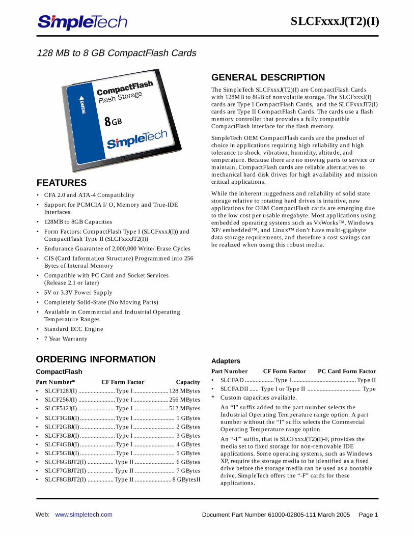
PACKAGE DIMENSIONS AND PIN LOCATIONS (continued)
Length .................. 3.370±.008 in (85.6±0.20 mm)
Width .................... 2.126±.004 in (54.0±0.10 mm)
Thickness ............ .1968 in max. (5.0 mm max.)
.196 .130
.138
1.738
2.126
3.37
0
Len
gth
of
CF
1.43
3
Adapter for CompactFlash Type I and II to PC Card Type II (Typical)

SLCFxxxJ(T2)(I) COMPACTFLASH
Document Part Number 61000-02805-111 March 2005 Page 5
PIN ASSIGNMENTS
PC Card Memory ModePin Signal Pin
Num Name Type1 GND Ground2 D03 I/O3 D04 I/O4 D05 I/O5 D06 I/O6 D07 I/O7 -CE1 I8 A10 I9 -OE I
10 A09 I11 A08 I12 A07 I13 VCC Power14 A06 I15 A05 I16 A04 I17 A03 I18 A02 I19 A01 I20 A00 I21 D00 I/O22 D01 I/O23 D02 I/O24 WP O25 -CD2 O26 -CD1 O27 D11 I/O28 D12 I/O29 D13 I/O30 D14 I/O31 D15 I/O32 -CE2 I33 -VS1 O34 -IORD I35 -IOWR I36 -WE I37 RDY/-BSY O38 VCC Power39 -CSEL I40 -VS2 O41 RESET I42 -WAIT O43 -INPACK O44 -REG I45 BVD2 I/O46 BVD1 I/O47 D08 I/O48 D09 I/O49 D10 I/O50 GND Ground
PC Card I/O ModePin Signal Pin
Num Name Type1 GND Ground2 D03 I/O3 D04 I/O4 D05 I/O5 D06 I/O6 D07 I/O7 -CE1 I8 A10 I9 -OE I
10 A09 I11 A08 I12 A07 I13 VCC Power14 A06 I15 A05 I16 A04 I17 A03 I18 A02 I19 A01 I20 A00 I21 D00 I/O22 D01 I/O23 D02 I/O24 -IOIS16 O25 -CD2 O26 -CD1 O27 D11 I/O28 D12 I/O29 D13 I/O30 D14 I/O31 D15 I/O32 -CE2 I33 -VS1 O34 -IORD I35 -IOWR I36 -WE I37 IREQ O38 VCC Power39 -CSEL I40 -VS2 O41 RESET I42 -WAIT O43 -INPACK O44 -REG I45 -SPKR I/O46 -STSCHG I/O47 D08 I/O48 D09 I/O49 D10 I/O50 GND Ground
True IDE ModePin Signal Pin
Num Name Type1 GND Ground2 D03 I/O3 D04 I/O4 D05 I/O5 D06 I/O6 D07 I/O7 -CS0 I8 A10 I9 -SELATA I
10 A09* I11 A08* I12 A07* I13 VCC Power14 A06* I15 A05* I16 A04* I17 A03* I18 A02 I19 A01 I20 A00 I21 D00 I/O22 D01 I/O23 D02 I/O24 -IOCS16* O25 -CD2 O26 -CD1 O27 D11 I/O28 D12 I/O29 D13 I/O30 D14 I/O31 D15 I/O32 -CS1 I33 -VS1* O34 -IORD I35 -IOWR I36 -WE I37 INTRQ O38 VCC Power39 -CSEL I40 -VS2* O41 -RESET I42 IORDY O43 Not Used O44 Not Used I45 -DASP I/O46 -PDIAG I/O47 D08 I/O48 D09 I/O49 D10 I/O50 GND Ground
* Signals marked with an asterisk are not used in IDE Mode.

SLCFxxxJ(T2)(I) COMPACTFLASH
Document Part Number 61000-02805-111 March 2005 Page 6
Pin PC Card CF
35 GND -IOWR
36 -CD1 -WE
37 D11 -RDY/-BSY/-IREQ
38 D12 VCC
39 D13 -CSEL
40 D14 -VS2
41 D15 RESET
42 -CE2 -WAIT
43 -VS1 -INPACK
44 -IORD -REG
45 -IOWR BVD2/DASP
46 BVD1/-PDIAG
47 D08
48 D09
49 D10
50 GND
51 VCC
52
53
54
55
56
57 -VS2
58 RESET
59 -WAIT
60 -INPACK
61 -REG
62 BVD2
63 -STSCHG
64 D08
65 D09
66 D10
67 -CD2
68 GND
Pin PC Card CF
1 GND GND
2 D03 D03
3 D04 D04
4 D05 D05
5 D06 D06
6 D07 D07
7 -CE1 -CE1
8 A10 A10
9 -OE -OE
10 A09
11 A09 A08
12 A08 A07
13 VCC
14 A06
15 -WE A05
16 -RDY/-BSY/-IREQ A04
17 VCC A03
18 A02
19 A01
20 A00
21 D00
22 A07 D01
23 A06 D02
24 A05 WP/-IOIS16
25 A04 -CD2
26 A03 -CD1
27 A02 D11
28 A01 D12
29 A00 D13
30 D00 D14
31 D01 D15
32 D02 -CE2
33 WP/-IOIS16 -VS1
34 GND -IORD
PINOUT OF THE PC CARD TO CF ADAPTER

SLCFxxxJ(T2)(I) COMPACTFLASH
Document Part Number 61000-02805-111 March 2005 Page 7
Signal Name
BVD2(PC Card Memory Mode)
-SPKR(PC Card I/O Mode)
-DASP(True IDE Mode)
-CD1, -CD2(PC Card Memory Mode)
-CD1, -CD2(PC Card I/O Mode)
-CD1, -CD2(True IDE Mode)
D15-D00(PC Card Memory Mode)
D15-D00(PC Card I/O Mode
D15-D00(True IDE Mode)
-IOWR(PC Card Memory Mode)
-IOWR(PC Card I/O Mode)
-IOWR(True IDE Mode)
-IORD(PC Card Memory Mode)
-IORD(PC Card I/O Mode)
-IORD(True IDE Mode)
-WE(PC Card Memory Mode)
-WE(PC Card I/O Mode)
-WE(True IDE Mode)
Dir
I/O
○ ○ ○
○ ○ ○
O
○ ○ ○
○ ○ ○
I/O
○ ○ ○
○ ○ ○
I
○ ○ ○
○ ○ ○
○ ○ ○
I
○ ○ ○
I
○ ○ ○
○ ○ ○
Pin
45
○ ○ ○ ○ ○ ○ ○
○ ○ ○ ○ ○ ○ ○
26, 25
○ ○ ○ ○ ○ ○ ○
○ ○ ○ ○ ○ ○ ○
31, 30, 29, 28,27, 49, 48, 47,
6, 5, 4, 3, 2,
○ ○ ○ ○ ○ ○ ○
23, 22, 21
○ ○ ○ ○ ○ ○ ○
35
○ ○ ○ ○ ○ ○ ○
○ ○ ○ ○ ○ ○ ○
○ ○ ○ ○ ○ ○ ○
34
○ ○ ○ ○ ○ ○ ○
36
○ ○ ○ ○ ○ ○ ○
○ ○ ○ ○ ○ ○ ○
Description
This output line is always driven to a high state in Memory Mode since abattery is not required for this product.
This output line is always driven to a high state in I/O Mode since thisproduct produces no audio.
In the True IDE Mode, this input/output is the Disk Active/Slave Presentsignal in the Master/Slave handshake protocol.
These Card Detect pins are connected to ground on the card. They are usedby the host to determine that the card is fully inserted into the socket.
This signal is the same as Memory Mode.
These signals are not used in IDE Mode.
These lines carry the data, commands, and status information between thehost and the controller. D00 is the LSB of the Even Byte of the Word. D08 isthe LSB of the Odd Byte of the Word.
This signal is the same as the PC Card Memory Mode signal.
In True IDE Mode, all Task File operations occur in byte mode on the loworder bus D00-D07 while all data transfers are 16 bit using D00-D15.
This signal is not used in this mode.
The I/O Write strobe pulse is used to clock I/O data onto the data busand into the card controller registers. The clocking occurs on thenegative to positive edge of the signal (trailing edge).
In True IDE Mode, this signal has the same function as in PC Card I/OMode.
This signal is not used in this mode.
This is an I/O Read strobe generated by the host. This signal gates I/Odata onto the bus from the card.
In True IDE Mode, this signal has the same function as in PC Card I/OMode.
This is a signal driven by the host and used for strobing memory write datainto the registers. It is also used for writing the configuration registers.
In PC Card I/O Mode, this signal is used for writing the configurationregisters.
In True IDE Mode, this input signal is not used and should be connected toVCC.
SIGNAL DESCRIPTIONS
(continued)

SLCFxxxJ(T2)(I) COMPACTFLASH
Document Part Number 61000-02805-111 March 2005 Page 8
Dir
I
○ ○ ○
○ ○ ○
O
○ ○ ○
○ ○ ○
I
○ ○ ○
○ ○ ○
I
○ ○ ○
○ ○ ○
Signal Name
-OE(PC Card Memory Mode)
-OE(PC Card I/O Mode)
-OE(True IDE Mode)
RDY/-BSY(PC Card Memory Mode)
-IREQ(PC Card I/O Mode)
INTRQ(True IDE Mode)
A10-A0(PC Card Memory Mode)
A10-A0(PC Card I/O Mode)
A2-A0(True IDE Mode)
-CE1, -CE2(PC Card Memory Mode)Card Enable
-CE1, -CE2(PC Card I/O Mode)Card Enable
-CS0, -CS1(True IDE Mode)
Pin
9
○ ○ ○ ○ ○ ○ ○
○ ○ ○ ○ ○ ○ ○
37
○ ○ ○ ○ ○ ○ ○
○ ○ ○ ○ ○ ○ ○
8, 10, 11, 12,14, 15, 16, 17,
○ ○ ○ ○ ○ ○ ○
18, 19, 20
○ ○ ○ ○ ○ ○ ○
27, 28, 29
7, 32
○ ○ ○ ○ ○ ○ ○
○ ○ ○ ○ ○ ○ ○
Description
This is an Output Enable strobe generated by the host interface. It is usedto read data from the card in Memory Mode and to read the CIS andconfiguration registers.
In PC Card I/O Mode, this signal is used to read the CIS and configurationregisters.
To enable True IDE Mode, this input should be grounded by the host.
In Memory Mode this signal is set high when the card is ready toaccept a new data transfer operation and held low when the card isbusy. The host memory card socket must provide a pull-up resistor. Atpower up and at reset, the RDY/-BSY signal is held low (busy) untilthe card has completed its power up or reset function. No access ofany type should be made to the card during this time. The RDY/-BSYsignal is held high (disabled from being busy) whenever the followingcondition is true: the card has been powered up with RESETcontinuously disconnected or asserted high.
After the card has been configured for I/O operation, this signal is used asthe active low interrupt request. This line is strobed low to generate a pulsemode interrupt or held low for a level mode interrupt.
In True IDE Mode, this signal is the active high interrupt request to thehost.
These address lines along with the -REG signal are used to select thefollowing: the I/O port address registers within the card, the memorymapped port address registers within the card, a byte in the card’sinformation structure and the card’s configuration control and statusregisters.
This signal is the same as the PC Card Memory Mode signal.
In True IDE Mode only, A2:A0 are used to select the one of eight registersin the Task File. The remaining address lines should be grounded.
These input signals are used both to select the card and to indicate to thecard whether a byte or a word operation is being performed. -CE2 alwaysaccesses the odd byte of the word. -CE1 accesses the even byte or the oddbyte of the word depending on A0 and -CE2. A multiplexing scheme basedon A0, -CE1, -CE2 allows 8 bit hosts to access all data on D0-D7.
This signal is the same as the PC Card Memory Mode signal.
In the True IDE Mode, -CS0 is the chip select for the task file registers while-CS2 is used to select the Alternate Status Register and the Device ControlRegister.
SIGNAL DESCRIPTIONS (continued)
(continued)
SLCFxxxJ(T2)(I) COMPACTFLASH
Document Part Number 61000-02805-111 March 2005 Page 9
Dir
I
○ ○ ○
○ ○ ○
I
○ ○ ○
○ ○ ○
O
○ ○ ○
○ ○ ○
O
○ ○ ○
○ ○ ○
I/O
○ ○ ○
○ ○ ○
Pin
39
○ ○ ○ ○ ○ ○ ○
○ ○ ○ ○ ○ ○ ○
44
○ ○ ○ ○ ○ ○ ○
○ ○ ○ ○ ○ ○ ○
24
○ ○ ○ ○ ○ ○ ○
○ ○ ○ ○ ○ ○ ○
43
○ ○ ○ ○ ○ ○ ○
○ ○ ○ ○ ○ ○ ○
46
○ ○ ○ ○ ○ ○ ○
○ ○ ○ ○ ○ ○ ○
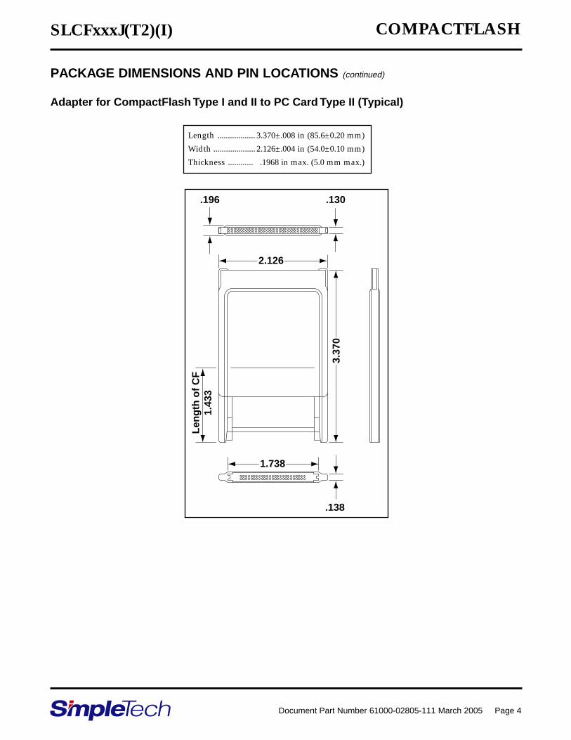
Signal Name
-CSEL(PC Card Memory Mode)
-CSEL(PC Card I/O Mode)
-CSEL(True IDE Mode)
-REG(PC Card Memory Mode)Attribute Memory Select
-REG(PC Card I/O Mode)
Not Used(True IDE Mode)
WP(PC Card Memory Mode)Write Protect
-IOIS16(PC Card I/O Mode)
-IOIS16(True IDE Mode)
-INPACK(PC Card Memory Mode)
-INPACK(PC Card I/O Mode)Input Acknowledge
Not Used(True IDE Mode)
BVD1(PC Card Memory Mode)
-STSCHG(PC Card I/O Mode)Status Changed
-PDIAG(True IDE Mode)
Description
This signal is not used for this mode.
This signal is not used for this mode.
This internally pulled up signal is used to configure the card as a Master ora Slave. When the pin is grounded, the card is configured as a Master.When the pin is open, the card is configured as a Slave.
This signal is distinguishes between accesses to Common Memory (high)and Register Attribute Memory (low).
The signal must also be active (low) during I/O Cycles when the I/Oaddress is on the bus.
This signal is not used in True IDE mode.
The card does not have a write protect switch; therefore, this signal is heldlow after the completion of the reset initialization sequence.
A low signal indicates that a 16 bit or odd byte only operation can beperformed at the addressed port.
Not defined in IDE Mode.
This signal is not used in this mode.
The Input Acknowledge signal is asserted by the card when it is selectedand responding to an I/O read cycle at the address that is on the bus. Thehost uses this signal to control the enable of any input data buffers betweenthe card and the host’s CPU.
This signal is not used in True IDE mode.
This signal is asserted high as since a battery is not used with this product.
This signal is asserted low to alert the host to changes in the RDY/-BSYand Write Protect states. Its use is controlled by the Card Configurationand Status Register.
In True IDE Mode, this input/output signal is the Pass Diagnostic signal inthe Master/Slave handshake protocol.
SIGNAL DESCRIPTIONS (continued)
(continued)

SLCFxxxJ(T2)(I) COMPACTFLASH
Document Part Number 61000-02805-111 March 2005 Page 10
Signal Name
-WAIT(PC Card Memory Mode)
-WAIT(PC Card I/O Mode)
IORDY(True IDE Mode)
GND(PC Card Memory Mode)
GND(PC Card I/O Mode)
GND(True IDE Mode)
VCC(PC Card Memory Mode)
VCC(PC Card I/O Mode)
VCC(True IDE Mode)
RESET(PC Card Memory Mode)
RESET(PC Card I/O Mode)
-RESET(True IDE Mode)
-VS1-VS2(PC Card Memory Mode)
-VS1-VS2(PC Card I/O Mode)
-VS1-VS2(True IDE Mode)
Dir
O
○ ○ ○
○ ○ ○
—
○ ○ ○
○ ○ ○
—
○ ○ ○
○ ○ ○
I
○ ○ ○
○ ○ ○
O
○ ○ ○
○ ○ ○
Pin
42
○ ○ ○ ○ ○ ○ ○
○ ○ ○ ○ ○ ○ ○
1, 50
○ ○ ○ ○ ○ ○ ○
○ ○ ○ ○ ○ ○ ○
13, 38
○ ○ ○ ○ ○ ○ ○
○ ○ ○ ○ ○ ○ ○
41
○ ○ ○ ○ ○ ○ ○
○ ○ ○ ○ ○ ○ ○
3340
○ ○ ○ ○ ○ ○ ○
○ ○ ○ ○ ○ ○ ○
Description
This signal is not used by the card, and is pulled up to VCC through a 4.7Kohm resistor.
This signal is not used by the card, and is pulled up to VCC through a 4.7Kohm resistor.
This signal is not used by the card, and is pulled up to VCC through a 4.7Kohm resistor.
Ground
Ground
Ground
+5 V or 3.3V power
+5 V or 3.3V power
+5 V or 3.3V power
When RESET is high, this signal resets the card. The card is reset only atpower up if this signal is left high or open from power-up. The card canalso be reset when the soft reset bit in the Card Configuration OptionRegister is set.
This signal is the same as the PC Card Memory Mode signal.
In the True IDE Mode this input pin is the active low hardware reset fromthe host.
-VS1 is grounded, and -VS2 is not connected so that the card CIS can beread at either 3.3 volts or 5.0 volts.
This signal is the same for all models.
This signal is not used in IDE Mode.
SIGNAL DESCRIPTIONS (continued)

SLCFxxxJ(T2)(I) COMPACTFLASH
Document Part Number 61000-02805-111 March 2005 Page 11
ABSOLUTE MAXIMUM RATINGS
Parameter Symbol Value UnitVoltage on any pin w.r.t. Vss Vin, Vout -0.5 to VCC+0.5 VStorage Temperature range Tstg -65 to +150 °C
RECOMMENDED OPERATING CONDITIONS
Parameter Symbol Min Typ Max UnitCommercial operating temperature Ta 0 25 70 °CIndustrial operating temperature Ta -40 — 85 °CVCC voltage VCC 4.75 5.0 5.25 V
3.18 3.3 3.465
PERFORMANCE
Item ValueData Write/Erase Endurance 2 million cycles min.Data reliability 1 in 1014 bits, readData retention 10 years
RELIABILITY
ENVIRONMENTAL CHARACTERISTICSItem ValueShock 2K G, half-sine, 0.330 ms to 0.750 ms
(per MIL-STD-202G Method 213B, Condition A)Vibration 30 G 10Hz-2KHz
(per MIL-STD-202G Method 204D 20 min/sweep, 12 sweeps/axis)Humidity 85°C 95% RH, 5.5V, 500 hrs
Item PerformanceData Transfer Rate To/From Host 16.7 MBytes/s (burst)Sustained Read up to 5 MBytes/sSustained Write up to 5 MBytes/s
Capacity C H S128MB 980 8 32256MB 980 16 32512MB 993 16 631GB 1986 16 632GB 3970 16 633GB 6022 16 634GB 7964 16 635GB 10038 16 636GB 12046 16 637GB 14054 16 638GB 16062 16 63
C=cylinders; H=heads; S=sectors/track
CHS PARAMETERS

SLCFxxxJ(T2)(I) COMPACTFLASH
Document Part Number 61000-02805-111 March 2005 Page 12
DC CHARACTERISTICS-1 (Ta=0 to 70°C for commercial temperature parts, -40 to 85°C for industrialtemperature parts; VCC=3.3V +5% or -3.6%)
Symbol Parameter Min Max Units NotesVIL Input LOW Voltage -0.3 +0.8 V
VIH Input HIGH Voltage 2.0 VCC+0.3 V
VOL Output LOW Voltage 0.45 V at 4mA
VOH Output HIGH Voltage 2.4 V at 1mA
ICC Operating CurrentSleep mode 800 µAOperating 30 mA
ILI Input Leakage Current 10 µA
ILO Output Leakage Current 1 µA
CI/O Input/output Capacitance 25 pF

SLCFxxxJ(T2)(I) COMPACTFLASH
Document Part Number 61000-02805-111 March 2005 Page 13
DC CHARACTERISTICS-2 (Ta=0 to 70°C for commercial temperature parts, -40 to 85°C for industrialtemperature parts; VCC=5V±5%)
Symbol Parameter Min Max Units NotesVIL Input LOW Voltage -0.3 +0.8 V
VIH Input HIGH Voltage 2.0 VCC+0.3 V
VOL Output LOW Voltage 0.8 V at 4mA
VOH Output HIGH Voltage 4.0 V at 1mA
ICC Operating Current, VCC=5.0VSleep mode 1200 µAOperating 30 mA
ILI Input Leakage Current 10 µA
ILO Output Leakage Current 2 µA
CI/O Input/output Capacitance 25 pF

SLCFxxxJ(T2)(I) COMPACTFLASH
Document Part Number 61000-02805-111 March 2005 Page 14
Item Symbol IEEE Symbol Min. (ns) Max. (ns)
Read Cycle Time tc(R) tAVAV 250
Address Access Time ta(A) tAVQV 250
Card Enable Access Time ta(CE) tELQV 250
Output Enable Access Time ta(OE) tGLQV 125
Output Disable Time from -CE tdis(CE) tEHQZ 100
Output Disable Time from -OE tdis(OE) tGHQZ 100
Address Setup Time tsu(A) tAVGL 30
Output Enable Time from -CE ten(CE) tELQNZ 5
Output Enable Time from -OE ten(OE) tGLQNZ 5
Data Valid from Address Change tv(A) tAXQX 0
Address Hold Time th(A) — 20
-CE Setup Time tsu(CE) — 0
-CE Hold Time th(CE) — 20
AC CHARACTERISTICS (Ta=0 to 70°C for commercial temperature parts, -40 to 85°C for industrialtemperature parts; VCC=5V±5% or VCC=3.3V +5% or -3.6%)
Attribute Memory Read AC Characteristics
Attribute Memory Read Timings
(continued)
A0-A10
-REG
-CE2/-CE1
-OE
D0-D15
tc(R)
tsu(A)
ta(CE)
ta(A)
tv(A)th(CE)
th(A)
ten(CE)
ta(OE)
ten(OE)
tdis(CE)
tdis(OE)
valid output
-WE, -IOWR, -IORD: High Fix
tsu(CE)
SLCFxxxJ(T2)(I) COMPACTFLASH
Document Part Number 61000-02805-111 March 2005 Page 15
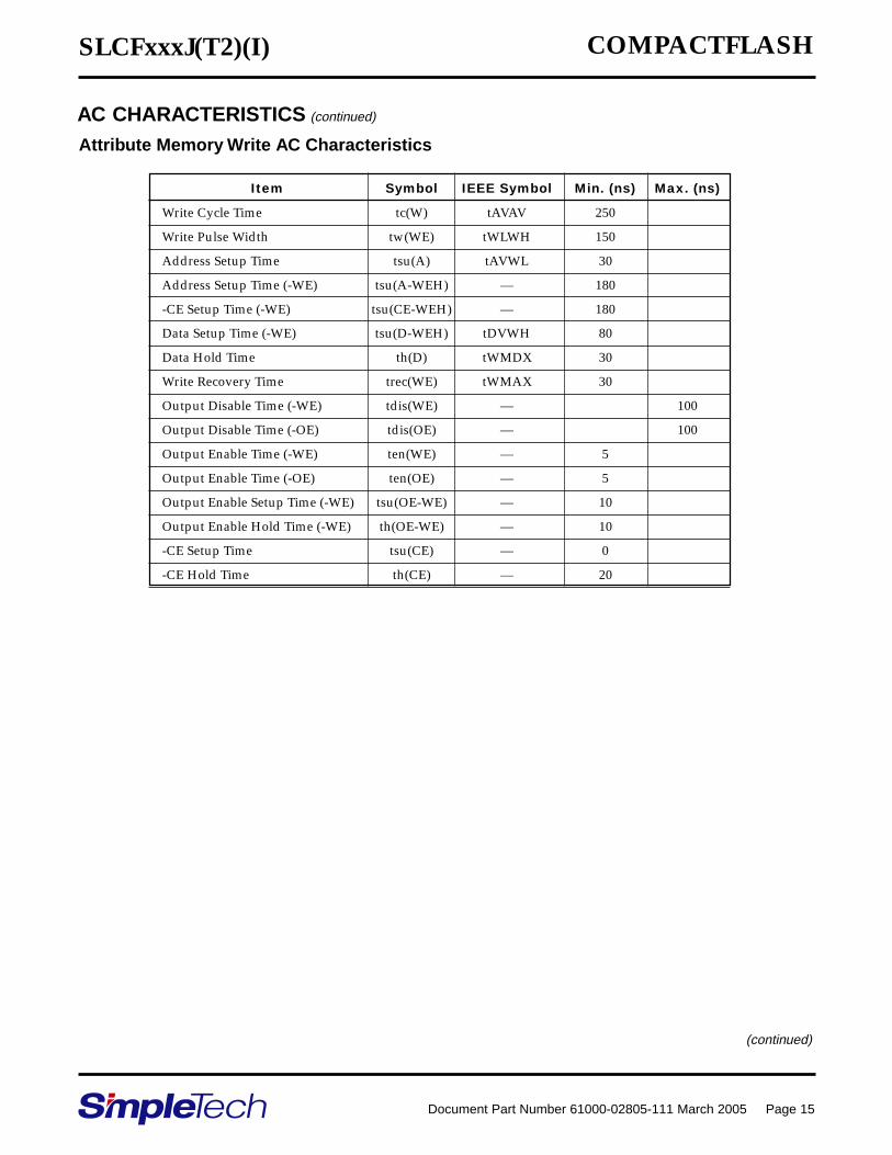
Item Symbol IEEE Symbol Min. (ns) Max. (ns)
Write Cycle Time tc(W) tAVAV 250
Write Pulse Width tw(WE) tWLWH 150
Address Setup Time tsu(A) tAVWL 30
Address Setup Time (-WE) tsu(A-WEH) — 180
-CE Setup Time (-WE) tsu(CE-WEH) — 180
Data Setup Time (-WE) tsu(D-WEH) tDVWH 80
Data Hold Time th(D) tWMDX 30
Write Recovery Time trec(WE) tWMAX 30
Output Disable Time (-WE) tdis(WE) — 100
Output Disable Time (-OE) tdis(OE) — 100
Output Enable Time (-WE) ten(WE) — 5
Output Enable Time (-OE) ten(OE) — 5
Output Enable Setup Time (-WE) tsu(OE-WE) — 10
Output Enable Hold Time (-WE) th(OE-WE) — 10
-CE Setup Time tsu(CE) — 0
-CE Hold Time th(CE) — 20
Attribute Memory Write AC Characteristics
AC CHARACTERISTICS (continued)
(continued)

SLCFxxxJ(T2)(I) COMPACTFLASH
Document Part Number 61000-02805-111 March 2005 Page 16
Attribute Memory Write Timings
AC CHARACTERISTICS (continued)
(continued)
A0 to A10
-REG
-WE
-CE2/-CE1
-OE
Din
tc(W)
tsu(A) trec(WE)
tsu(D-WEH)
Data In Valid
th(D)
tw(WE)

SLCFxxxJ(T2)(I) COMPACTFLASH
Document Part Number 61000-02805-111 March 2005 Page 17
Item Symbol IEEE Symbol Min. (ns) Max. (ns)
Data Delay after -IORD td(IORD) tIGLQV 100
Data Hold following -IORD th(IORD) tIGHQX 0
-IORD Width Time tw(IORD) tIGLIGH 165
Address Setup before -IORD tsuA(IORD) tAVIGL 70
Address Hold following -IORD thA(IORD) tIGHAX 20
-CE Setup before -IORD tsuCE(IORD) tELIGL 5
-CE Hold following -IORD thCE(IORD) tIGHEH 20
-REG Setup before -IORD tsuREG(IORD) tRGLIGL 5
-REG Hold following -IORD thREG(IORD) tIGHRGH 0
-INPACK Delay Falling from -IORD tdfINPACK(IORD) tIGLIAL 0 45
-INPACK Delay Rising from -IORD tdrINPACK(IORD) tIGHIAH 45
-IOIS16 Delay Falling from Address tdfIOIS16(ADR) tAVISL 35
-IOIS16 Delay Rising from Address tdrIOIS16(ADR) tAVISH 35
I/O Access Read AC Characteristics
AC CHARACTERISTICS (continued)
(continued)
SLCFxxxJ(T2)(I) COMPACTFLASH
Document Part Number 61000-02805-111 March 2005 Page 18
I/O Access Read Timings
AC CHARACTERISTICS (continued)
(continued)
A0 to A10
-REG
-CE2/-CE1
-IORD
-INPACK
-IOIS16
D0 to D15
tw(IORD)
td(IORD)
th(IORD)
valid output
-WE, -OE, -IOWR: High Fix
tsuA(IORD)
tdrINPACK(IORD)
tsuREG(IORD)
tsuCE(IORD)
tdfINPACK(IORD)
thA(IORD)
thREG(IORD)
thCE(IORD)
tdrIOIS16(ADR)
tdfIOIS16(ADR)
SLCFxxxJ(T2)(I) COMPACTFLASH
Document Part Number 61000-02805-111 March 2005 Page 19
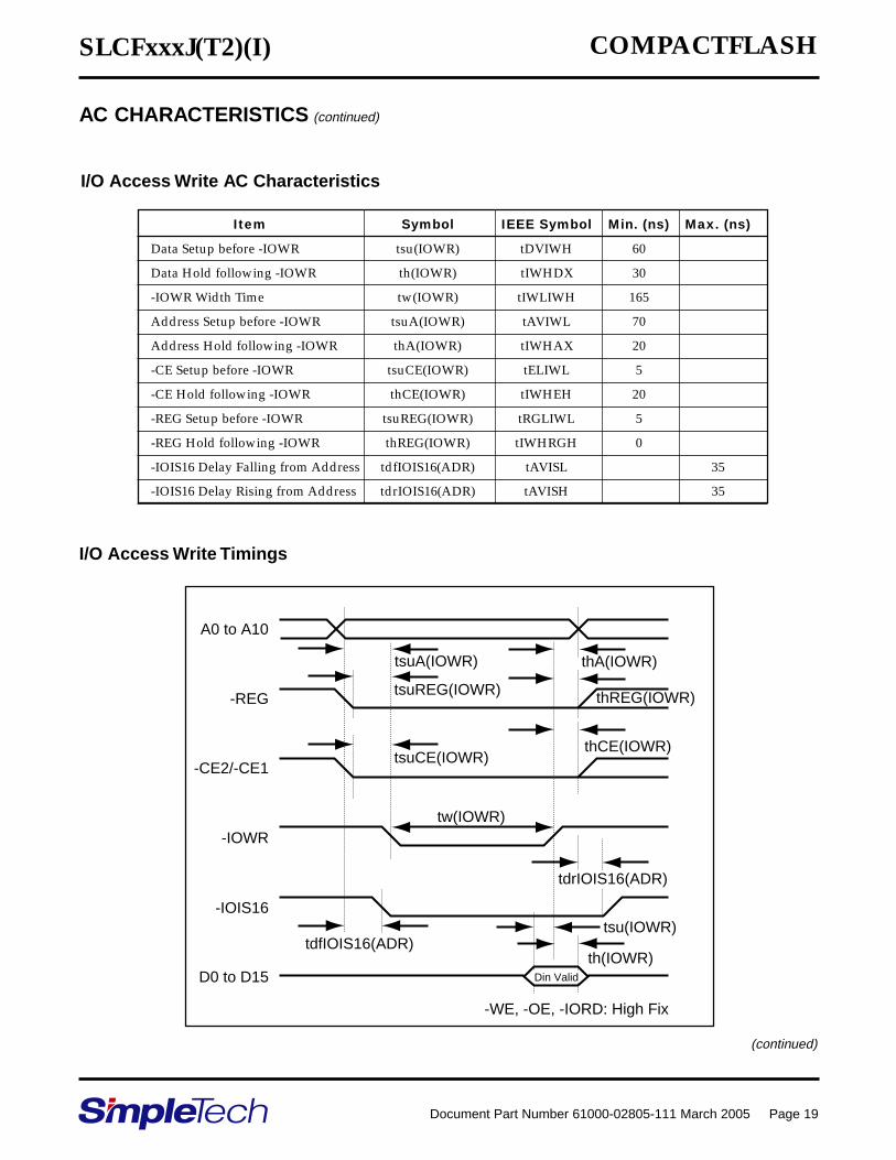
Item Symbol IEEE Symbol Min. (ns) Max. (ns)
Data Setup before -IOWR tsu(IOWR) tDVIWH 60
Data Hold following -IOWR th(IOWR) tIWHDX 30
-IOWR Width Time tw(IOWR) tIWLIWH 165
Address Setup before -IOWR tsuA(IOWR) tAVIWL 70
Address Hold following -IOWR thA(IOWR) tIWHAX 20
-CE Setup before -IOWR tsuCE(IOWR) tELIWL 5
-CE Hold following -IOWR thCE(IOWR) tIWHEH 20
-REG Setup before -IOWR tsuREG(IOWR) tRGLIWL 5
-REG Hold following -IOWR thREG(IOWR) tIWHRGH 0
-IOIS16 Delay Falling from Address tdfIOIS16(ADR) tAVISL 35
-IOIS16 Delay Rising from Address tdrIOIS16(ADR) tAVISH 35
I/O Access Write AC Characteristics
I/O Access Write Timings
AC CHARACTERISTICS (continued)
(continued)
A0 to A10
-REG
-CE2/-CE1
-IOWR
-IOIS16
D0 to D15
tw(IOWR)
tsuA(IOWR)
tsuREG(IOWR)
tsuCE(IOWR)
thA(IOWR)
thREG(IOWR)
thCE(IOWR)
tdrIOIS16(ADR)
tdfIOIS16(ADR)th(IOWR)
-WE, -OE, -IORD: High Fix
tsu(IOWR)
Din Valid

SLCFxxxJ(T2)(I) COMPACTFLASH
Document Part Number 61000-02805-111 March 2005 Page 20
AC CHARACTERISTICS (continued)
(continued)
Register Access AC Characteristics for True IDE
PIO Mode Access AC Characteristics for True IDE
Parameter Symbol Mode0 Mode1 Mode2 Mode3 Mode4 UnitCycle time (min) t0 600 383 330 180 120 nsAddress valid to -IORD/-IOWR (min) t1 70 50 30 30 25 nssetup-IORD/-IOWR pulse width 8bit (min) t2 290 290 290 80 70 ns-IORD/-IOWR recovery time (min) t2i — — — 70 25 ns-IOWR data setup (min) t3 60 45 30 30 20 ns-IOWR data hold (min) t4 30 20 15 10 10 ns-IORD data setup (min) t5 50 35 20 20 20 ns-IORD data hold (min) t6 5 5 5 5 5 ns-IORD data tristate (max) t6z 30 30 30 30 30 nsAddress valid to -IOCS16 assert. (max) t7 90 50 40 n/a n/a nsAddress valid to -IOCS16 release(max) t8 60 45 30 n/a n/a ns-IORD/-IOWR to address valid t9 20 15 10 10 10 nshold
Parameter Symbol Mode0 Mode1 Mode2 Mode3 Mode4 UnitCycle time (min) t0 600 383 240 180 120 nsAddress valid to -IORD/-IOWR (min) t1 70 50 30 30 25 nssetup-IORD/-IOWR pulse width 16bit (min) t2 165 125 100 80 70 ns-IORD/-IOWR recovery time (min) t2i - - - 70 25 ns-IOWR data setup (min) t3 60 45 30 30 20 nsIOWR data hold (min) t4 30 20 15 10 10 ns-IORD data setup (min) t5 50 35 20 20 20 ns-IORD data hold (min) t6 5 5 5 5 5 ns-IORD data tristate (max) t6z 30 30 30 30 30 nsAddress valid to -IOCS16 assert. (max) t7 90 50 40 n/a n/a nsAddress valid to -IOCS16 release(max) t8 60 45 30 n/a n/a ns-IORD/-IOWR to address valid t9 20 15 10 10 10 nshold

SLCFxxxJ(T2)(I) COMPACTFLASH
Document Part Number 61000-02805-111 March 2005 Page 21
AC CHARACTERISTICS (continued)
True IDE Mode Access Read/Write Timings
ADDR valid
-IORD/-IOWR
D15 to D0 (Write)
D15 to D0 (Read)
-IOIS16
IORDY
t0
t1t2
t9
t8
t2i
t3
t5 t6
t6Z
t4
t7
SLCFxxxJ(T2)(I) COMPACTFLASH
Document Part Number 61000-02805-111 March 2005 Page 22
HOST ACCESS SPECIFICATION
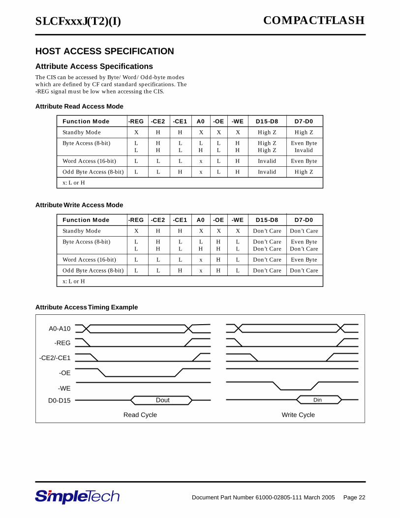
Attribute Access SpecificationsThe CIS can be accessed by Byte/Word/Odd-byte modeswhich are defined by CF card standard specifications. The-REG signal must be low when accessing the CIS.
Attribute Read Access Mode
Function Mode -REG -CE2 -CE1 A0 -OE -WE D15-D8 D7-D0
Standby Mode X H H X X X High Z High Z
Byte Access (8-bit) L H L L L H High Z Even ByteL H L H L H High Z Invalid
Word Access (16-bit) L L L x L H Invalid Even Byte
Odd Byte Access (8-bit) L L H x L H Invalid High Z
x: L or H
Attribute Write Access Mode
Function Mode -REG -CE2 -CE1 A0 -OE -WE D15-D8 D7-D0
Standby Mode X H H X X X Don’t Care Don’t Care
Byte Access (8-bit) L H L L H L Don’t Care Even ByteL H L H H L Don’t Care Don’t Care
Word Access (16-bit) L L L x H L Don’t Care Even Byte
Odd Byte Access (8-bit) L L H x H L Don’t Care Don’t Care
x: L or H
Attribute Access Timing Example
A0-A10
-REG
-CE2/-CE1
-OE
-WE
D0-D15 Dout
Read Cycle Write Cycle
Din
SLCFxxxJ(T2)(I) COMPACTFLASH
Document Part Number 61000-02805-111 March 2005 Page 23
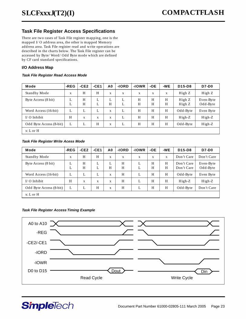
Task File Register Access SpecificationsThere are two cases of Task File register mapping, one is themapped I/O address area, the other is mapped Memoryaddress area. Task File register read and write operations aredescribed in the charts below. The Task File register can beaccessed by Byte/Word/Odd Byte mode which are definedby CF card standard specifications.
I/O Address Map
Task File Register Access Timing Example
Task File Register Read Access Mode
Mode -REG -CE2 -CE1 A0 -IORD -IOWR -OE -WE D15-D8 D7-D0
Standby Mode x H H x x x x x High Z High Z
Byte Access (8 bit) L H L L L H H H High Z Even-ByteL H L H L H H H High Z Odd-Byte
Word Access (16-bit) L L L x L H H H Odd-Byte Even Byte
I/O Inhibit H x x x L H H H High-Z High-Z
Odd Byte Access (8-bit) L L H x L H H H Odd-Byte High-Z
x: L or H
Mode -REG -CE2 -CE1 A0 -IORD -IOWR -OE -WE D15-D8 D7-D0
Standby Mode x H H x x x x x Don’t Care Don’t Care
Byte Access (8 bit) L H L L H L H H Don’t Care Even-ByteL H L H H L H H Don’t Care Odd-Byte
Word Access (16-bit) L L L x H L H H Odd-Byte Even Byte
I/O Inhibit H x x x H L H H High-Z High-Z
Odd Byte Access (8-bit) L L H x H L H H Odd-Byte Don’t Care
x: L or H
A0 to A10
-REG
-CE2/-CE1
-IORD
-IOWR
D0 to D15 Dout Din
Read Cycle Write Cycle
Task File Register Write Acess Mode
SLCFxxxJ(T2)(I) COMPACTFLASH
Document Part Number 61000-02805-111 March 2005 Page 24
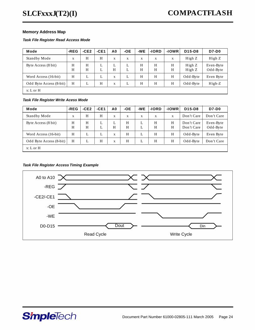
Memory Address Map
Task File Register Write Acess Mode
Task File Register Access Timing Example
Task File Register Read Access Mode
Mode -REG -CE2 -CE1 A0 -OE -WE -IORD -IOWR D15-D8 D7-D0
Standby Mode x H H x x x x x High Z High Z
Byte Access (8 bit) H H L L L H H H High Z Even-ByteH H L H L H H H High Z Odd-Byte
Word Access (16-bit) H L L x L H H H Odd-Byte Even Byte
Odd Byte Access (8-bit) H L H x L H H H Odd-Byte High-Z
x: L or H
Mode -REG -CE2 -CE1 A0 -OE -WE -IORD -IOWR D15-D8 D7-D0
Standby Mode x H H x x x x x Don’t Care Don’t Care
Byte Access (8 bit) H H L L H L H H Don’t Care Even-ByteH H L H H L H H Don’t Care Odd-Byte
Word Access (16-bit) H L L x H L H H Odd-Byte Even Byte
Odd Byte Access (8-bit) H L H x H L H H Odd-Byte Don’t Care
x: L or H
A0 to A10
-REG
-CE2/-CE1
-OE
-WE
D0-D15 Dout
Read Cycle Write Cycle
Din

SLCFxxxJ(T2)(I) COMPACTFLASH
Document Part Number 61000-02805-111 March 2005 Page 25
True IDE ModeThe card is configured in a True IDE mode of operation whenthe -OE input signal is asserted GND by the host at powerup. In the True IDE mode, Attribute Registers are notaccessible from the host. The data register is accessed in word(16-bit) mode at power up. The card permits 8-bit accesses ifthe host issues a Set Feature Command to put the device in 8-bit mode.
True IDE Mode Read I/O Function
Mode -CE2 -CE1 A0 to A2 -IORD -IOWR D15-D8 D7-D0
Invalid Mode L L x x x High Z High Z
Standby Mode H H x x x High Z High Z
Data Register Access H L 0 L H Odd-Byte Even-Byte
Alternate Status Access L H 6h L H High Z Status Out
Other Task File Access H L 1-7h L H High Z Data
x: L or H
True IDE Mode Write I/O Function
Mode -CE2 -CE1 A0 to A2 -IORD -IOWR D15-D8 D7-D0
Invalid Mode L L x x x Don’t Care Don’t Care
Standby Mode H H x x x Don’t Care Don’t Care
Data Register Access H L 0 H L Odd-Byte Even-Byte
Control Register Access L H 6h H L Don’t Care Control In
Other Task File Access H L 1-7h H L Don’t Care Data
x: L or H
True IDE Mode I/O Access Timing Example
A0 to A2
-CE2/-CE1
-IORD
-IOWR
-IOIS16
D0 to D15 Dout
Read Cycle
Din
Write Cycle

SLCFxxxJ(T2)(I) COMPACTFLASH
Document Part Number 61000-02805-111 March 2005 Page 26
CIS INFORMATION (TYPICAL)-------
0000: Code 01, link 03
D9 01 FF
--------
Tuple CISTPL_DEVICE (01), length 3 (03) at offset 0
Device type is FUNCSPEC
Device speed is 250ns
Write protect switch is not in control
Device size is 2K bytes
--------
0005: Code 1C, link 04
03 D9 01 FF
--------
Tuple CISTPL_DEVICE_OC (1C), length 4 (04) at offset 5
Device conditions: minimum cycle with WAIT at Vcc = 3.3V
Device type is FUNCSPEC
Device speed is 250ns
Write protect switch is not in control
Device size is 2K bytes
--------
000B: Code 18, link 02
DF 01
--------
Tuple CISTPL_JEDEC_C (18), length 2 (02) at offset B
Device 0 JEDEC id: Manufacturer DF, ID 01
--------
000F: Code 20, link 04
4D 01 00 01
--------
Tuple CISTPL_MANFID (20), length 4 (04) at offset F
Manufacturer # 0x014D hardware rev 1.00
--------
0015: Code 15, link 13
04 01 53 54 49 00 46 6C 61 73 68 20 37 2E 30 2E
30 00 FF
--------
Tuple CISTPL_VERS_1 (15), length 19 (13) at offset 15
Major version 4, minor version 1
Product Information:
Manufacturer: "STI"
Product name: "Flash X.Y.Z"
--------
002A: Code 21, link 02
04 01
--------
Tuple CISTPL_FUNCID (21), length 2 (02) at offset 2A
Function code 04 (Fixed Disk), system init 01
--------
002E: Code 22, link 02
01 01
--------
Tuple CISTPL_FUNCE (22), length 2 (02) at offset 2E
This is an PC Card ATA Disk
--------
0032: Code 22, link 03
02 0C 0F
--------
Tuple CISTPL_FUNCE (22), length 3 (03) at offset 32
Vpp is not required
This is a silicon device
Identify Drive Model/Serial Number is guaranteed unique
Low-Power Modes supported: Sleep Standby Idle
Drive automatically minimizes power
All modes include 3F7 or 377
Index bit is not supported
-IOIS16 is unspecified in Twin configurations

SLCFxxxJ(T2)(I) COMPACTFLASH
Document Part Number 61000-02805-111 March 2005 Page 27
--------
0037: Code 1A, link 05
01 03 00 02 0F
--------
Tuple CISTPL_CONFIG (1A), length 5 (05) at offset 37
Last valid configuration index is 3
Configuration Register Base Address is 200
Configuration Registers Present:
Configuration Option Register at 200
Card Configuration and Status Register at 202
Pin Replacement Register at 204
Socket and Copy Register at 206
--------
003E: Code 1B, link 08
C0 C0 A1 01 55 08 00 20
--------
Tuple CISTPL_CFTABLE_ENTRY (1B), length 8 (08) at offset 3E
Configuration Table Index is 00 (default)
Interface type is Memory
BVDs not active, WP not active, RdyBsy active
Wait signal support required
Vcc Power Description:
Nom V = 5.0 V
map 2048 bytes of memory to card address 0
Miscellaneous Features:
Max Twins 0, -Audio, -ReadOnly, +PowerDown
--------
0048: Code 1B, link 06
00 01 21 B5 1E 4D
--------
Tuple CISTPL_CFTABLE_ENTRY (1B), length 6 (06) at offset 48
Configuration Table Index is 00
Vcc Power Description:
Nom V = 3.30 V
Peak I = 45.0 mA
--------
0050: Code 1B, link 0A
C1 41 99 01 55 64 F0 FF FF 20
--------
Tuple CISTPL_CFTABLE_ENTRY (1B), length 10 (0A) at offset 50
Configuration Table Index is 01 (default)
Interface type is I/O
BVDs not active, WP not active, RdyBsy active
Wait signal support not required
Vcc Power Description:
Nom V = 5.0 V
Decode 4 I/O lines, bus size 8 or 16
IRQ may be shared, pulse and level mode interrupts are supported
Interrupts in mask FFFF are supported
Miscellaneous Features:
Max Twins 0, -Audio, -ReadOnly, +PowerDown
--------
005C: Code 1B, link 06
01 01 21 B5 1E 4D
--------
Tuple CISTPL_CFTABLE_ENTRY (1B), length 6 (06) at offset 5C
Configuration Table Index is 01
Vcc Power Description:
Nom V = 3.30 V
Peak I = 45.0 mA
--------
SLCFxxxJ(T2)(I) COMPACTFLASH
Document Part Number 61000-02805-111 March 2005 Page 28
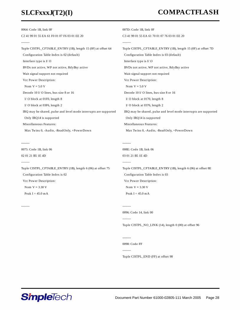
0064: Code 1B, link 0F
C2 41 99 01 55 EA 61 F0 01 07 F6 03 01 EE 20
--------
Tuple CISTPL_CFTABLE_ENTRY (1B), length 15 (0F) at offset 64
Configuration Table Index is 02 (default)
Interface type is I/O
BVDs not active, WP not active, RdyBsy active
Wait signal support not required
Vcc Power Description:
Nom V = 5.0 V
Decode 10 I/O lines, bus size 8 or 16
I/O block at 01F0, length 8
I/O block at 03F6, length 2
IRQ may be shared, pulse and level mode interrupts are supported
Only IRQ14 is supported
Miscellaneous Features:
Max Twins 0, -Audio, -ReadOnly, +PowerDown
--------
0075: Code 1B, link 06
02 01 21 B5 1E 4D
--------
Tuple CISTPL_CFTABLE_ENTRY (1B), length 6 (06) at offset 75
Configuration Table Index is 02
Vcc Power Description:
Nom V = 3.30 V
Peak I = 45.0 mA
--------
007D: Code 1B, link 0F
C3 41 99 01 55 EA 61 70 01 07 76 03 01 EE 20
--------
Tuple CISTPL_CFTABLE_ENTRY (1B), length 15 (0F) at offset 7D
Configuration Table Index is 03 (default)
Interface type is I/O
BVDs not active, WP not active, RdyBsy active
Wait signal support not required
Vcc Power Description:
Nom V = 5.0 V
Decode 10 I/O lines, bus size 8 or 16
I/O block at 0170, length 8
I/O block at 0376, length 2
IRQ may be shared, pulse and level mode interrupts are supported
Only IRQ14 is supported
Miscellaneous Features:
Max Twins 0, -Audio, -ReadOnly, +PowerDown
--------
008E: Code 1B, link 06
03 01 21 B5 1E 4D
--------
Tuple CISTPL_CFTABLE_ENTRY (1B), length 6 (06) at offset 8E
Configuration Table Index is 03
Vcc Power Description:
Nom V = 3.30 V
Peak I = 45.0 mA
--------
0096: Code 14, link 00
--------
Tuple CISTPL_NO_LINK (14), length 0 (00) at offset 96
--------
0098: Code FF
--------
Tuple CISTPL_END (FF) at offset 98
SLCFxxxJ(T2)(I) COMPACTFLASH
Document Part Number 61000-02805-111 March 2005 Page 29
CONFIGURATION REGISTERSPECIFICATIONThis card supports four configuration registers for thepurpose of the configuration and observation of the card.These registers can be used in memory card mode and I/Ocard mode. In True IDE mode, these registers can not beused.
Configuration Option Register(Address 200h)This register is used to configure and observe the status ofthe card, and to issue soft resets to the card.
bit7 bit6 bit5 bit4 bit3 bit2 bit1 bit0
SRESET LevlREQ INDEX (bits 0-5)
Initial Value: 00h
Name R/W Function
SRESET (HOST->) R/W Setting this bit to “1” places the card in the reset state. This operation is equal to a hardreset, except this bit is not cleared.
LevlREQ (HOST->) R/W This bit is set to “0” when pulse mode interrupt is selected, and to “1” when level modeinterupt is selected.
INDEX (HOST->) R/W These bits are used to select the operation mode of the card. (See table below.) At power on,hard reset, and soft reset, this data is “000000” for the purpose of Memory card interfacerecognition, and access to CIS.
INDEX bit5 4 3 2 1 0 Card Mode Task File Register Address Mapping Mode
0 0 0 0 0 0 Memory Card 0h to Fh, 400h to 7FFh Memory Mapped
0 0 0 0 0 1 I/O Card xx0h to xxFh Contiguous I/O Mapped
0 0 0 0 1 0 I/O Card 1F0h to 1F7h, 3F6h to 3F7h Primary I/O Mapped
0 0 0 0 1 1 I/O Card 170h to 177h, 376h to 377h Secondary I/O Mapped

SLCFxxxJ(T2)(I) COMPACTFLASH
Document Part Number 61000-02805-111 March 2005 Page 30
Configuration and Status Register(Address 202h)This register is used for observing the card state.
bit7 bit6 bit5 bit4 bit3 bit2 bit1 bit0
CHGED SIGCHG IOIS8 0 0 PWD INTR 0
Initial Value: 00h
Name R/W Function
CHGED (CARD->) R This bit indicates that CRDY/-BSY bit on Pin Replacement register is set to “1”. When theCHGED bit is set to “1”, the -STSCHG pin is held low if the SIGCHG bit is also set to “1”and the card configured for the I/O interface.
SIGCHG (HOST->) R/W This bit is set or reset by the host for enabling and disabling the status change signal (-STSCHGpin). When the card is configured to I/O card interface and this bit is set to “1”, -STSCHG pinis controlled by CHGED bit. If this bit is set to “0”, -STSCHG pin is kept high when the card isconfigured for I/O.
IOIS8 (HOST->) R/W The host sets this field to “1” when it can provide I/O cycles only with an 8 bit data bus (D7 toD0).
PWD (HOST->) R/W When this bit is set to “1”, the card enters sleep state (power down mode). When this bit is resetto “0”, the card transfers to idle state (active mode).
INTR (CARD->) R This bit indicates the internal state of the interrupt request. The bit is available whether theI/O card interface has been configured or not. This signal remains true until the conditionwhich caused the interrupt request has been serviced. If interrupts are disabled by the -IENbit in the Device Control Register, this bit is a zero.

SLCFxxxJ(T2)(I) COMPACTFLASH
Document Part Number 61000-02805-111 March 2005 Page 31
Pin Replacement Register(Address 204h)This register is used for providing the signal state of -IREQwhen the card is configured as the I/O card interface.
bit7 bit6 bit5 bit4 bit3 bit2 bit1 bit0
0 0 CRDY/-BSY CWProt 1 1 RRDY/-BSY RWProt
Initial Value: 0Ch
Name R/W Function
CRDY/-BSY (HOST->) R/W This bit is set to “1” when the RRDY/-BSY bit changes state. This bit may also bewritten by the host.
CWProt (HOST->) R This bit is set to “1” when the RWProt changes state. This bit may also be written bythe host.
RRDY/-BSY (HOST->) R/W This bit is used to determine the internal state of the RDY/BSY signal. This bit may beused to determine the state of the Ready/Busy as this pin has been reallocated for useas interrupt request on an I/O card.
RWProt (HOST->) R This bit indicates the write protect status. When set, indicates write protect. Whencleared, indicates that write is enabled.
Socket and Copy Register(Address 206h)This read and write register is used to identify the card fromother cards. This register should be set by the host before thiscard’s Configuration Option register is set.
bit7 bit6 bit5 bit4 bit3 bit2 bit1 bit0
0 0 0 DRV# 1 1` 0 0
Initial Value: 00h
Name R/W Function
DRV# (HOST->) R/W These fields are used to configure mulitple cards. When the host configures multiple cards,the card’s copy number is written in this field. In this way, the host can perform the card’smaster/slave organization.

SLCFxxxJ(T2)(I) COMPACTFLASH
Document Part Number 61000-02805-111 March 2005 Page 32
TASK FILE REGISTERSPECIFICATIONThese registers are used for reading and writing data to thecard. These registers are mapped four types by theconfiguration of INDEX in Configuration Option register. Afifth mapping, True IDE, is configured at power up if -OE isheld low.
-REG A10 A9-A4 A3 A2 A1 A0 Offset -OE=L -WE=L
1 0 X 0 0 0 0 0 Data register Data register
1 0 X 0 0 0 1 1 Error register Feature register
1 0 X 0 0 1 0 2 Sector Count register Sector Count register
1 0 X 0 0 1 1 3 Sector No. register Sector No. register
1 0 X 0 1 0 0 4 Cylinder Low register Cylinder Low register
1 0 X 0 1 0 1 5 Cylinder High register Cylinder High register
1 0 X 0 1 1 0 6 Drive Head register Drive Head register
1 0 X 0 1 1 1 7 Status register Command register
1 0 X 1 0 0 0 8 Dup. Even RD Data reg. Dup. Even WR Data reg.
1 0 X 1 0 0 1 9 Dup. Odd RD Data reg. Dup. Odd WR Data reg.
1 0 X 1 1 0 1 D Dup. Error register Dup. Feature register
1 0 X 1 1 1 0 E Alt Status register Device Ctl register
1 0 X 1 1 1 1 F Drive Address register Reserved
1 1 X X X X 0 8 Even Data register Even Data register
1 1 X X X X 1 9 Odd Data register Odd Data register
Memory Map (INDEX=0)
SLCFxxxJ(T2)(I) COMPACTFLASH
Document Part Number 61000-02805-111 March 2005 Page 33
-REG A10-A4 A3 A2 A1 A0 Offset -IORD=L -IOWR=L
0 X 0 0 0 0 0 Data register Data register
0 X 0 0 0 1 1 Error register Feature register
0 X 0 0 1 0 2 Sector Count register Sector Count register
0 X 0 0 1 1 3 Sector No. register Sector No. register
0 X 0 1 0 0 4 Cylinder Low register Cylinder Low register
0 X 0 1 0 1 5 Cylinder High register Cylinder High register
0 X 0 1 1 0 6 Drive Head register Drive Head register
0 X 0 1 1 1 7 Status register Command register
0 X 1 0 0 0 8 Dup. Even RD Data reg. Dup. Even WR Data reg.
0 X 1 0 0 1 9 Dup. Odd RD Data reg. Dup. Odd WR Data reg.
0 X 1 1 0 1 D Dup. Error register Dup. Feature register
0 X 1 1 1 0 E Alt Status register Device Ctl register
0 X 1 1 1 1 F Drive Address register Reserved
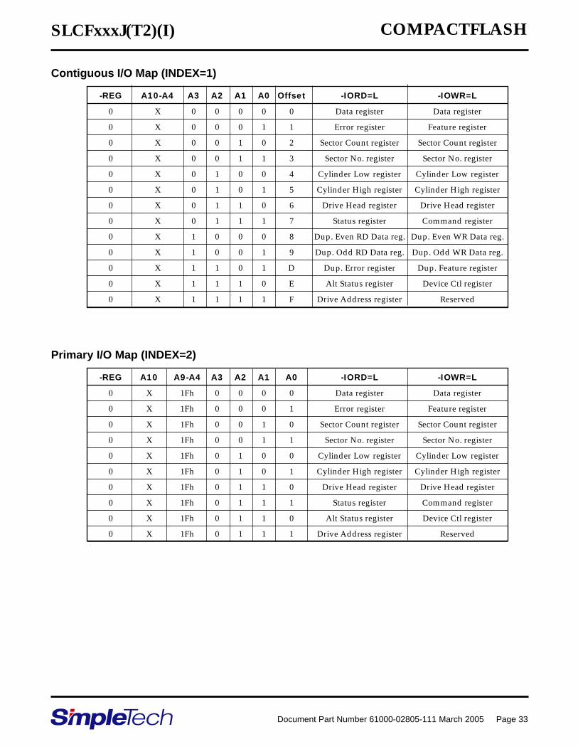
Contiguous I/O Map (INDEX=1)
-REG A10 A9-A4 A3 A2 A1 A0 -IORD=L -IOWR=L
0 X 1Fh 0 0 0 0 Data register Data register
0 X 1Fh 0 0 0 1 Error register Feature register
0 X 1Fh 0 0 1 0 Sector Count register Sector Count register
0 X 1Fh 0 0 1 1 Sector No. register Sector No. register
0 X 1Fh 0 1 0 0 Cylinder Low register Cylinder Low register
0 X 1Fh 0 1 0 1 Cylinder High register Cylinder High register
0 X 1Fh 0 1 1 0 Drive Head register Drive Head register
0 X 1Fh 0 1 1 1 Status register Command register
0 X 1Fh 0 1 1 0 Alt Status register Device Ctl register
0 X 1Fh 0 1 1 1 Drive Address register Reserved
Primary I/O Map (INDEX=2)

SLCFxxxJ(T2)(I) COMPACTFLASH
Document Part Number 61000-02805-111 March 2005 Page 34
-REG A10 A9-A4 A3 A2 A1 A0 -IORD=L -IOWR=L
0 X 17h 0 0 0 0 Data register Data register
0 X 17h 0 0 0 1 Error register Feature register
0 X 17h 0 0 1 0 Sector Count register Sector Count register
0 X 17h 0 0 1 1 Sector No. register Sector No. register
0 X 17h 0 1 0 0 Cylinder Low register Cylinder Low register
0 X 17h 0 1 0 1 Cylinder High register Cylinder High register
0 X 17h 0 1 1 0 Drive Head register Drive Head register
0 X 17h 0 1 1 1 Status register Command register
0 X 37h 0 1 1 0 Alt Status register Device Ctl register
0 X 37h 0 1 1 1 Drive Address register Reserved
Secondary I/O Map (INDEX=3)
-CE2 -CE1 A2 A1 A0 -IORD=0 -IOWR=0
1 0 0 0 0 Data register Data register
1 0 0 0 1 Error register Feature register
1 0 0 1 0 Sector Count register Sector Count register
1 0 0 1 1 Sector No. register Sector No. register
1 0 1 0 0 Cylinder Low register Cylinder Low register
1 0 1 0 1 Cylinder High register Cylinder High register
1 0 1 1 0 Drive Head register Drive Head register
1 0 1 1 1 Status register Command register
0 1 1 1 0 Alt Status register Device Control register
0 1 1 1 1 Drive Address register Reserved
True IDE Mode I/O Map (-OE held low at power up)
SLCFxxxJ(T2)(I) COMPACTFLASH
Document Part Number 61000-02805-111 March 2005 Page 35
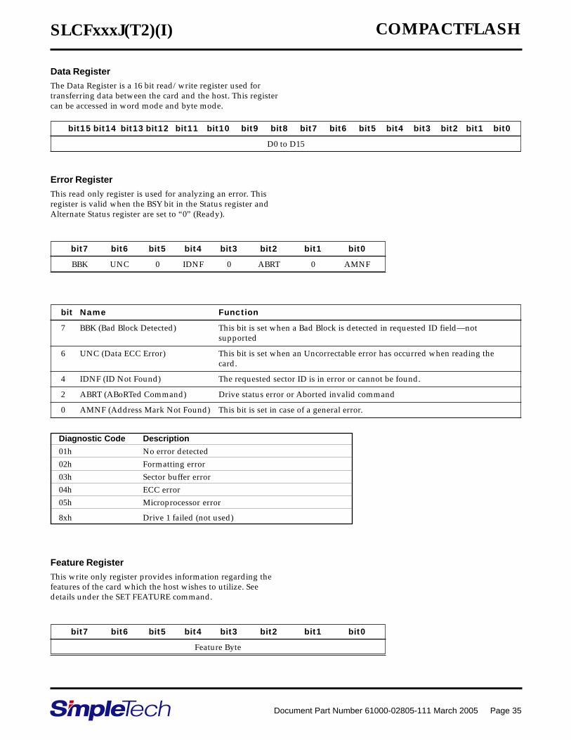
Data RegisterThe Data Register is a 16 bit read/write register used fortransferring data between the card and the host. This registercan be accessed in word mode and byte mode.
bit15 bit14 bit13 bit12 bit11 bit10 bit9 bit8 bit7 bit6 bit5 bit4 bit3 bit2 bit1 bit0
D0 to D15
Error Register
This read only register is used for analyzing an error. Thisregister is valid when the BSY bit in the Status register andAlternate Status register are set to “0” (Ready).
bit7 bit6 bit5 bit4 bit3 bit2 bit1 bit0
BBK UNC 0 IDNF 0 ABRT 0 AMNF
bit Name Function
7 BBK (Bad Block Detected) This bit is set when a Bad Block is detected in requested ID field—notsupported
6 UNC (Data ECC Error) This bit is set when an Uncorrectable error has occurred when reading thecard.
4 IDNF (ID Not Found) The requested sector ID is in error or cannot be found.
2 ABRT (ABoRTed Command) Drive status error or Aborted invalid command
0 AMNF (Address Mark Not Found) This bit is set in case of a general error.
Feature RegisterThis write only register provides information regarding thefeatures of the card which the host wishes to utilize. Seedetails under the SET FEATURE command.
bit7 bit6 bit5 bit4 bit3 bit2 bit1 bit0
Feature Byte
Diagnostic Code Description
01h No error detected
02h Formatting error
03h Sector buffer error
04h ECC error
05h Microprocessor error
8xh Drive 1 failed (not used)

SLCFxxxJ(T2)(I) COMPACTFLASH
Document Part Number 61000-02805-111 March 2005 Page 36
Sector Count RegisterThis register contains the numbers of sectors of datarequested to be transferred on a read or write operationbetween the host and the card. If the value in the register is 0,a count of 256 sectors is indicated.
bit7 bit6 bit5 bit4 bit3 bit2 bit1 bit0
Sector Count Byte
Cylinder Low Register
In CHS mode (LBA=0), this register contains the low orderbits of the starting cylinder address. In LBA mode, it containsbits 15:8 of the LBA.
bit7 bit6 bit5 bit4 bit3 bit2 bit1 bit0
Cylinder Low Byte or bits 15:8 of the LBA
Cylinder High RegisterIn CHS mode (LBA=0), this register contains the high orderbits of the starting cylinder address. In LBA mode, it containsbits 23:16 of the LBA.
bit7 bit6 bit5 bit4 bit3 bit2 bit1 bit0
Cylinder High Byte or bits 23:16 of the LBA
Sector Number Register
When the LBA bit in the Drive/Head register is 0, thisregister contains the starting sector number for any mediaaccess. When the LBA bit is set to 1, this register contains bits7:0 of the LBA for any media access.
bit7 bit6 bit5 bit4 bit3 bit2 bit1 bit0
Sector Number Byte or bits 7:0 of the LBA
SLCFxxxJ(T2)(I) COMPACTFLASH
Document Part Number 61000-02805-111 March 2005 Page 37
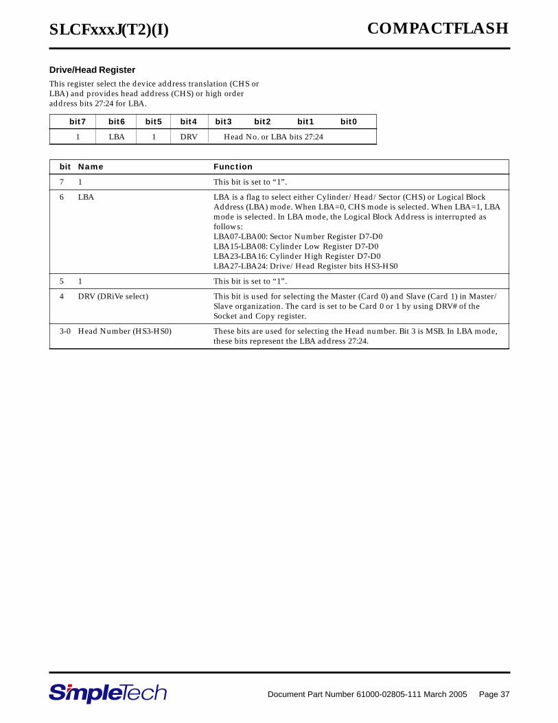
Drive/Head RegisterThis register select the device address translation (CHS orLBA) and provides head address (CHS) or high orderaddress bits 27:24 for LBA.
bit7 bit6 bit5 bit4 bit3 bit2 bit1 bit0
1 LBA 1 DRV Head No. or LBA bits 27:24
bit Name Function
7 1 This bit is set to “1”.
6 LBA LBA is a flag to select either Cylinder/Head/Sector (CHS) or Logical BlockAddress (LBA) mode. When LBA=0, CHS mode is selected. When LBA=1, LBAmode is selected. In LBA mode, the Logical Block Address is interrupted asfollows:LBA07-LBA00: Sector Number Register D7-D0LBA15-LBA08: Cylinder Low Register D7-D0LBA23-LBA16: Cylinder High Register D7-D0LBA27-LBA24: Drive/Head Register bits HS3-HS0
5 1 This bit is set to “1”.
4 DRV (DRiVe select) This bit is used for selecting the Master (Card 0) and Slave (Card 1) in Master/Slave organization. The card is set to be Card 0 or 1 by using DRV# of theSocket and Copy register.
3-0 Head Number (HS3-HS0) These bits are used for selecting the Head number. Bit 3 is MSB. In LBA mode,these bits represent the LBA address 27:24.

SLCFxxxJ(T2)(I) COMPACTFLASH
Document Part Number 61000-02805-111 March 2005 Page 38
bit7 bit6 bit5 bit4 bit3 bit2 bit1 bit0
BSY DRDY DWF DSC DRQ CORR IDX ERR
bit Name Function
7 BSY (BuSY) This bit is set when the card internal operation is executing. When this bit isset to “1”, other bits in this register are invalid.
6 DRDY (Drive ReaDY) If this bit and DSC bit are set to “1”, the card is capable of receiving the readand write or seek requests. If this bit is set to “0”, the card prohibits theserequests. On error, DRDY changes only after the host reads the Status Register.
5 DWF (Drive Write Fault) This bit is set if a fault occurs during the write process.
4 DSC (Drive Seek Complete) This bit is set when the requested sector was found.
3 DRQ (Data ReQuest) This bit is set when information can be transferred between the host and dataregister.
2 CORR (CORRected data) This bit is set when a correctable data error has occurred and the data has beencorrected.
1 IDX (InDeX) This bit is always set to “0”.
0 ERR (ERRor) This bit is set when the previous command has ended in some type of error.The error information is set in the Error register.
Alternate Status RegisterThis register is the same as the Status register except that-IREQ is not negated when data is read.
Status RegisterThis read only register indicates status of a commandexecution. When the BSY bit is “0”, the other bits are valid;when the BSY bit is “1”, the other bits are not valid. Whenthe register is read, the interrupt (-IREQ pin) is cleared.
Command Register
This write only register is used for writing the command thatexecutes the card’s operation. The command code is writtenin the command register after its parameters are written inthe Task File during the card ready state. See details underthe ATA COMMAND SPECIFICATIONS.

SLCFxxxJ(T2)(I) COMPACTFLASH
Document Part Number 61000-02805-111 March 2005 Page 39
Device Control RegisterThis write only register is used for controlling the interruptrequest and issuing an ATA soft reset to the card.
bit7 bit6 bit5 bit4 bit3 bit2 bit1 bit0
x x x x 1 SRST nIEN 0
bit Name Function
7-4 x Don’t care.
3 1 This bit is set to “1”.
2 SRST (Software ReSeT) This bit is set to “1” in order to force the card to perform an AT disk controlsoft reset operation.
1 nIEN (Interrupt ENable) When set to “0”, it enables interrupts to the host (using the -IREQ tri-statepin). When inactive (set to “1”) or drive is not selected, it disables all pendinginterrupts (-IREQ in high-Z). This bit is ignored in memory mode.
0 0 This bit is set to “0”.
Drive Address RegisterThis read only register is used for confirming the card’sstatus. This register is provided for compatibility with the ATdisk drive interface and it is not recommended that thisregister be mapped into the host’s I/O space because ofpotential conflicts on bit 7.
bit7 bit6 bit5 bit4 bit3 bit2 bit1 bit0
High-Z nWTG nHS3 nHS2 nHS1 nHS0 nDS1 nDS0
bit Name Function
7 x This bit is unused.
6 nWTG (WriTing Gate) This bit is unused.
5-2 nHS3-0 (Head Select 3-0) These bits are the negative value of the Head Select bits (bit 3 to 0) in theDrive/Head register
1 nDS1 (Drive Select 1) When set to “0”, drive 1 is active and selected.
0 nDS0 (Drive Select 0) When set to “0”, drive 0 is active and selected.

SLCFxxxJ(T2)(I) COMPACTFLASH
Document Part Number 61000-02805-111 March 2005 Page 40
No. Command set Code FR SC SN CY DR HD LBA
1 Check Power Mode E5h or 98h — Y — — Y — —
2 Execute Drive Diagnostic 90h — — — — Y** — —
3 Erase Sector(s) C0h — Y Y Y Y Y Y
4 Format Track 50h — Y — Y Y Y Y
5 Identify Drive ECh Y — — — Y — —
6 Idle E3h or 97h — Y — — Y — —
7 Idle Immediate E1h or 95h — — — — Y — —
8 Initialize Drive Parameters 91h — Y — — Y Y —
9 Read Buffer E4h — — — — Y — —
10 Read Multiple C4h — Y Y Y Y Y Y
11 Read Long Sector 22h or 23h* — — Y Y Y Y Y
12 Read Sector(s) 20h or 21h* — Y Y Y Y Y Y
13 Read Verify Sector(s) 40h or 41h* — Y Y Y Y Y Y
14 Recalibrate 1Xh — — — — Y — —
15 Request Sense 03h — — — — Y — —
16 Seek 7Xh — — Y Y Y Y Y
17 Set Features EFh — Y Y Y Y Y —
18 Set Multiple Mode C6h — Y — — Y — —
19 Set Sleep Mode E6h or 99h — — — — Y — —
20 Stand By E2h or 96h — Y — — Y — —
21 Stand By Immediate E0h or 94h — — — — Y — —
22 Translate Sector 87h — Y Y Y Y Y Y
23 Wear Level F5h — — — — Y Y —
24 Write Buffer E8h — — — — Y — —
25 Write Long Sector 32h or 33h* — Y Y Y Y Y Y
26 Write Multiple C5h — Y Y Y Y Y Y
27 Write Multiple w/o Erase CDh — Y Y Y Y Y Y
28 Write Sector(s) 30h or 31h* — Y Y Y Y Y Y
29 Write Sector(s) w/o Erase 38h — Y Y Y Y Y Y
30 Write Verify 3Ch — Y Y Y Y Y Y
FR=Features Register, SC=SectorCount Register (00h to FFh),SN=Sector Number Register (01hto 20h), CY=Cylinder Registers,DR=Drive bit of Drive/HeadRegister, HD=Head no. (0 to 3) of
ATA COMMAND SPECIFICATIONSThis table with the following paragraphs summarizes theATA command set.
Drive/Head Register,LBA=Logical Block AddressMode Supported.
Y—Set up.
“—” —Not set up.
* First command code=withretry,Second commandcode=without retry.
** Address to drive 0. Bothdrives execute command

SLCFxxxJ(T2)(I) COMPACTFLASH
Document Part Number 61000-02805-111 March 2005 Page 41
Check Power Mode(code: E5h or 98h)This command checks the power mode.
Execute Drive Diagnostic(code: 90h)This command performs the internal diagnostic testsimplemented by the card. See ERROR register for dianosticcodes.
Erase Sector(s)(code: C0h)This command is used to pre-erase and condition datasectors in advance.
Word Data Total DescriptionAddress Bytes
0 848AH 2 Value fixed by CFA (value=044AH for versions with the -F suffix)1 XXXXH 2 Default number of cylinders2 0000H 2 Reserved3 00XXH 2 Default number of heads4 XXXXH 2 Do not use this word. Before retirement, was number of unformatted bytes per track5 XXXXH 2 Do not use this word. Before retirement, was number of unformatted bytes per sector6 XXXXH 2 Default number of sectors per track
7-8 XXXXH 4 Number of sectors per card (word7=MSW, word 8 = LSW)9 0000H 2 Reserved
10-19 XXXXH 20 Serial Number (see table next page for definition)20 XXXXH 2 Do not use this word. Before retirement, was buffer type21 XXXXH 2 Do not use this word. Before retirement, was buffer size in 512 byte increments22 0004H 2 # of ECC bytes passed on Read/Write Long commands
23-46 XXXXH 48 Firmware revision and model number in ASCII (see table next page for definition)47 0001H 2 Maximum of 1 sector on Read/Write Multiple command48 0000H 2 Double Word not supported49 0200H 2 DMA not supported, LBA supported50 0000H 2 Reserved51 0200H 2 PIO data transfer cycle timing mode52 0000H 2 Single word DMA data transfer cycle timing mode (not supported)53 0003h 2 Words 54 - 58 and 64 - 70 are valid54 XXXXH 2 Number of Current Cylinders55 XXXXH 2 Number of Current Heads56 XXXXH 2 Number of Current Sectors Per Track57 XXXXH 2 LSW of the Current Capacity in Sectors58 XXXXH 2 MSW of the Current Capacity in Sectors59 010XH 2 Current Setting for Block Count=1 for R/W Multiple commands
60-61 XXXXH 4 Total number of sectors addressable in LBA Mode62 0000H 2 Single word DMA transfer not supported63 0000H 2 Multiword DMA modes not supported64 0003H 2 Advanced PIO modes supported (modes 3 and 4)65 0000H 2 Minimum multiword DMA transfer cycle time per word (ns)66 0000H 2 Recommended multiword DMA transfer cycle time per word (ns)67 0078H 2 Minimum PIO transfer without flow control68 0078H 2 Minimum PIO transfer with IORDY flow control
69-255 0000H 388 ReservedXXXXH: These values are dependent upon the the specific card.
Format Track(code: 50h)This command writes the desired head and cylinder of theselected drive with a vender unique data pattern (typically00h or FFh). This card accepts a sector buffer of data from thehost to follow the command with the same protocol as theWrite Sector Command although the information in thebuffer is not used.
Identify Drive(code: ECh)This command enables the host to receive parameterinformation from the card. (See table below.)
Identify Drive Information (Typical)

SLCFxxxJ(T2)(I) COMPACTFLASH
Document Part Number 61000-02805-111 March 2005 Page 42
Idle(code: E3h or 97h)This command causes the card to set BSY, enter the Idlemode, clear BSY, and generate an interrupt. If the sectorcount is non-zero, automatic power down mode is enabled. Ifthe sector count is zero, the automatic power down mode isdisabled.
Idle Immediate(code: E1h or 95h)This command causes the card to set BSY, enter the Idle(Read) mode, clear BSY, and generate an interrupt.
Initialize Drive Parameters(code: 91h)This command enables the host to set the number of sectorsper track and the number of heads per cylinder.
Read Buffer(code: E4h)This command enables the host to read the current contentsof the card’s sector buffer.
Read Multiple(code: C4h)This command performs similarly to the Read Sectorscommand. Interrupts are not generated on each sector, but onthe transfer of a block which contains the number of sectorsdefined by a Set Multiple command.
Read Long Sector(code: 22h or 23h)This command performs similarly to the Read Sector(s)command except that it returns 516 bytes of data instead of512 bytes.
Read Sector(s)(code: 20h or 21h)This command reads from 1 to 256 sectors as specified in theSector Count register. A sector count of 0 requests 256 sectors.The transfer begins at the sector specified in the SectorNumber register.
Read Verify Sector(s)(code: 40h or 41h)This command verifies one or more sectors on the card bytransferring data from the flash media to the data buffer inthe card and verifying that the ECC is correct. Thiscommandis identical to the Read Sectors command, exceptthat DRQ is never set and no data is transferred to the host.This
Recalibrate(code: 1Xh)The ComapactFlash performs only the interface timing andregister operations. When this command is issued, theComapactFlash sets BSY and waits for an appropriate lengthof time after which it clears BSY and issues an interrupt.When this command ends normally, the ComapactFlash isinitialized
Request Sense(code: 03h)This command requests an extended error code after acommand ends with an error. Refer to table below.
Code Description
00H No error detected
01H Self test OK (No error)
09H Miscellaneous Error - N/A
20H Invalid Command
21H Invalid Address (requestedHead or Sector invalid)
2FH Address Overflow (address toolarge)
35H, 36H Supply or generate Voltage Outof Tolerance
11H Uncorrectable ECC Error
18H Correctable ECC Error - N/A
05H, 30H-34H, 37H, 3EH Self Test Diagnostic Failed
10H, 14H ID Not Found - N/A
3AH Spare Sectors Exhausted
1FH Data Transfer Error / AbortedCommand
0CH, 38H, 3BH, 3CH, 3FH Corrupted Media Format - N/A
03H Write / Erase Failed - N/A
22H Power Level 1 Disabled
Serial Number Format (typical): Words 10-19
SimpleTech Proprietary Yr Day Hr Min SecSTI_J13C0 04 224 09 27 50
Firmware Revision: Words 23-26
mm/dd/yy
Model Number: Words 27-46
STI Flash X.Y.Z
Identify Drive Information (continued)(Serial Number, Firmware Revision, and Model Number)
SLCFxxxJ(T2)(I) COMPACTFLASH
Document Part Number 61000-02805-111 March 2005 Page 43
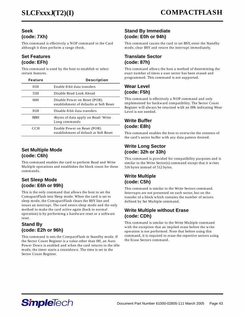
Seek(code: 7Xh)This command is effectively a NOP command to the Cardalthough it does perform a range check.
Set Features(code: EFh)This command is used by the host to establish or selectcertain features.
Feature Description
01H Enable 8-bit data transfers
55H Disable Read Look Ahead
66H Disable Power on Reset (POR)establishment of defaults at Soft Reset
81H Disable 8-bit data transfers
BBH 4bytes of data apply on Read/WriteLong commands
CCH Enable Power on Reset (POR)establishment of default at Soft Reset
Set Multiple Mode(code: C6h)This command enables the card to perform Read and WriteMultiple operations and establishes the block count for thesecommands.
Set Sleep Mode(code: E6h or 99h)This is the only command that allows the host to set theComapactFlash into Sleep mode. When the card is set tosleep mode, the ComapactFlash clears the BSY line andissues an interrupt. The card enters sleep mode and the onlymethod to make the card active again (back to normaloperation) is by performing a hardware reset or a softwarereset.
Stand By(code: E2h or 96h)This command is sets the CompactFlash in Standby mode. Ifthe Sector Count Register is a value other than 0H, an AutoPower Down is enabled and when the card returns to the idlemode, the timer starts a countdown. The time is set in theSector Count Register.
Stand By Immediate(code: E0h or 94h)This command causes the card to set BSY, enter the Standbymode, clear BSY and return the interrupt immediately.
Translate Sector(code: 87h)This command allows the host a method of determining theexact number of times a user sector has been erased andprogrammed. This command is not supported.
Wear Level(code: F5h)This command is effectively a NOP command and onlyimplemented for backward compatibility. The Sector CountRegister will always be returned with an 00h indicating WearLevel is not needed.
Write Buffer(code: E8h)This command enables the host to overwrite the contents ofthe card’s sector buffer with any data pattern desired.
Write Long Sector(code: 32h or 33h)This command is provided for compatibility purposes and issimilar to the Write Sector(s) command except that it writes516 bytes instead of 512 bytes.
Write Multiple(code: C5h)This command is similar to the Write Sectors command.Interrupts are not presented on each sector, but on thetransfer of a block which contains the number of sectorsdefined by Set Multiple command.
Write Multiple without Erase(code: CDh)This command is similar to the Write Multiple commandwith the exception that an implied erase before the writeoperation is not performed. Note that before using thiscommand, it is required to erase the repective sectors usingthe Erase Sectors command.

SLCFxxxJ(T2)(I) COMPACTFLASH
Document Part Number 61000-02805-111 March 2005 Page 44
Write Sector(s)(code: 30h or 31h)This command writes from 1 to 256 sectors as specified in theSector Count register. A sector count of zero requests 256sectors. The transfer begins at the sector specified in theSector Number register.
Write Sector(s) without Erase(code: 38h)This command is similar to the Write Sector(s) commandwith the exception that an implied erase before the writeoperation is not performed. Note that before using thiscommand, it is required to erase the repective sectors usingthe Erase Sectors command.
Write Verify(code: 3Ch)This command is similar to the Write Sector(s) commandexcept each sector is verified immediately after being written.
SLCFxxxJ(T2)(I) COMPACTFLASH
Document Part Number 61000-02805-111 March 2005 Page 45
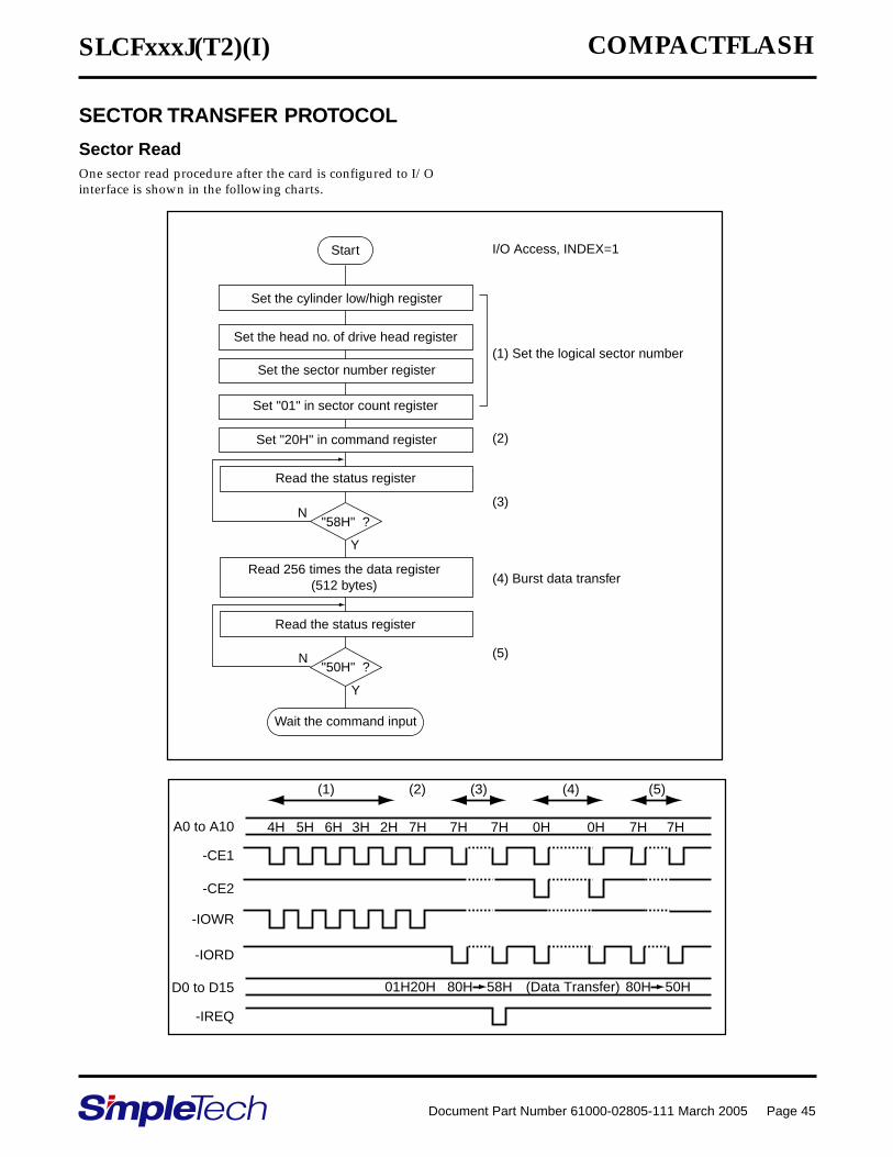
Start I/O Access, INDEX=1
(1) Set the logical sector number
(2)
(3)
(4) Burst data transfer
(5)
N
Y
Set the cylinder low/high register
Set the head no. of drive head register
Set the sector number register
Set "01" in sector count register
Set "20H" in command register
Read the status register
"58H" ?
Read the status register
"50H" ?
Wait the command input
Read 256 times the data register(512 bytes)
N
Y
SECTOR TRANSFER PROTOCOL
Sector ReadOne sector read procedure after the card is configured to I/Ointerface is shown in the following charts.
A0 to A10 4H 5H 6H 3H
(1) (2) (3) (4) (5)
2H 7H 7H 7H 0H 0H 7H 7H
-CE1
-CE2
-IOWR
-IORD
D0 to D15 01H20H 80H 58H 80H 50H(Data Transfer)
-IREQ

SLCFxxxJ(T2)(I) COMPACTFLASH
Document Part Number 61000-02805-111 March 2005 Page 46
Start I/O Access, INDEX=1
(1) Set the logical sector number
(2)
(3)
(4) Burst data transfer
(5)
N
Y
Set the cylinder low/high register
Set the head no. of drive head register
Set the sector number register
Set "01" in sector count register
Set "30H" in command register
Read the status register
"58H" ?
Read the status register
"50H" ?
Wait the command input
Write 256 times the data register(512 bytes)
N
Y
Sector WriteOne sector write procedure after the card is configured toI/O interface is shown in the following charts.
A0 to A10 4H 5H 6H 3H
(1) (2) (3) (4) (5)
2H 7H 7H 7H 0H 0H 7H 7H
-CE1
-CE2
-IOWR
-IORD
D0 to D15 01H30H 80H 58H 80H 50H(Data Transfer)
-IREQ

SLCFxxxJ(T2)(I) COMPACTFLASH
Document Part Number 61000-02805-111 March 2005 Page 47
REVISION HISTORY
Rev. Change Description from Previous Revision-101 1/1/04. Initial Release.-102 2/23/04. Sleep mode current at 3.3V corrected to 80µA
from 80mA. The operating current at 3.3V corrected to30mA from 3mA.
-103 2/23/04. IOL/IOH condition at 5.0V is removed.-104 3/16/04. Showpiece photo replaces Block Diagram.
General Description updated with new marketing copy.R/W speeds updated from 5.4/5.5MB/s to 5/5MB/s.64MB option removed.
-105 5/26/04. CHS Parameter table added. VCC(min)changed to 3.18V from 3.135V. VCC 5V tolerancechanged to 5% from 10%. Preliminary noticedremoved. CIS Information corrected. Disclaimer noticeadded.
-106 6/18/04. Features bullets on page 1 updated. PinAssignments for IDE Mode corrected to indicate whichpins are not used in IDE Mode. Pinout of the PC Cardto CF Adapter corrected to call out DASP and -PDIAG.Pin Description changes: -CD1 and -CD2 not used inIDE mode; -IOIS16 not used in IDE mode; -WAITdescription corrected to not used by card and pulledup by 4.7K ohm resistor. Performance rates for readand write described as sustained read and sustainedwrite. AC Characteristics VCC 3.3V operatingtolerances restated as +5% and -3.6% tolerances.Error register bit 0 Function “not supported” phraseremoved. DMA commands removed (paper only errorindicated that DMA was supported). Identify DriveInformation table updated to reflect DMA notsupported. “-F” p/n suffix selection added to notes ofthe Ordering Information. ATA-4 compatiblility added toFeatures. DC Characterists Sleep Mode valueschanged from 80uA to 800uA for 3.3V power supply,and 120uA to 1200uA for 5V power supply.
-107 7/9/04. Endurance increased from 300,000 cycles minto 2 million cycles min.
-108 7/22/04. “up to” added to sustained read and writedata rate performance.
-109 8/23/04. Definition for Serial #, Firmware Rev., andModel # in the Identify Drive Information table addedin callout. Identify Drive Table words 20, 21, 49, and 63corrected.
-110 10/14/04. Standard ECC, Endurance, and Warrantybullets added to Features on page 1.
-111 2/14/05. Shock parameter changed to 0.330ms to0.750ms from 11ms. 3/8/05. Humidity parameterchanged to 95% from 85%. 3/14/05. CHS valuesupdated.
SimpleTech Inc. reserves the right to make changes to specifications and product descriptions such as but not limited to numbers, parametersand other technical information contained herein without notice. Contact SimpleTech Inc. sales office to obtain the latest specifications.SimpleTech Inc. grants no warranty with respect to this Data Sheet, neither explicit nor implied, and it is not liable for direct or indirectdamages. Some States do not grant the exclusion of incidental damages and as such this statement may not be valid in such states. Theprovisions of this Data Sheet do not convey to the purchaser of the device any license under any patent rights or other intellectual propertyrights of SimpleTech Inc. or others.


![Certificate in Laptop Repairing - maharishiskills.commaharishiskills.com/wp-content/uploads/2019/03/... · • INTEGRATED CIRCUITS [IC] PCMCIA CARD &DVD DRIVE 1. What is pcmcia card?](https://img.dokumen.tips/doc/110x75/60845169f37fcd7f1b44f9e3/certificate-in-laptop-repairing-a-integrated-circuits-ic-pcmcia-card-dvd.jpg)