Embed Size (px)
Citation preview
SiT8921B
High Frequency, -55°C to +125°C Oscillator
Features ◼ Frequencies between 119.342001 MHz to 137 MHz
accurate to 6 decimal places
◼ Operating temperature from -55°C to 125°C
◼ Supply voltage of 1.8 V or 2.5 V to 3.3 V
◼ Excellent total frequency stability as low as ±20 ppm
◼ Low power consumption of 4.9 mA typical at 1.8V
◼ LVCMOS/LVTTL compatible output
◼ Industry-standard packages: 2.0 x 1.6, 2.5 x 2.0,
3.2 x 2.5, 5.0 x 3.2, 7.0 x 5.0 mm x mm
◼ Instant samples with Time Machine II and field
programmable oscillators
◼ RoHS and REACH compliant, Pb-free, Halogen-free and
Antimony-free
Applications ◼ Ruggedized equipment in harsh operating environment
Table 1. Electrical Characteristics
All Min and Max limits are specified over temperature and rated operating voltage with 15 pF output load unless otherwise stated. Typical values are at 25°C and nominal supply voltage.
Parameters Symbol Min. Typ. Max. Unit Condition
Frequency Range
Output Frequency Range f 119.342001 – 137 MHz Refer to Table 13 for the exact list of supported frequencies
Frequency Stability and Aging
Frequency Stability F_stab -20 – +20 ppm Inclusive of Initial tolerance at 25°C, 1st year aging at 25°C, and variations over operating temperature, rated power supply voltage and load (15 pF ± 10%).
-25 – +25 ppm
-30 – +30 ppm
-50 – +50 ppm
Operating Temperature Range
Operating Temperature Range T_use -55 – +125 °C Supply Voltage and Current Consumption
Supply Voltage Vdd 1.62 1.8 1.98 V 2.25 2.5 2.75 V
2.52 2.8 3.08 V
2.7 3.0 3.3 V
2.97 3.3 3.63 V
2.25 – 3.63 V
Current Consumption Idd – 6.2 8 mA No load condition, f = 125 MHz, Vdd = 2.8 V, 3.0 V or 3.3 V
– 5.4 7 mA No load condition, f = 125 MHz, Vdd = 2.5 V
– 4.9 6 mA No load condition, f = 125 MHz, Vdd = 1.8 V
OE Disable Current I_od – – 4.7 mA Vdd = 2.5 V to 3.3 V, OE = Low, Output in high Z state.
– – 4.5 mA Vdd = 1.8 V, OE = Low, Output in high Z state.
Standby Current I_std – 2.6 8.5 A Vdd = 2.8 V to 3.3V, ST = Low, Output is weakly pulled down
– 1.4 5.5 A Vdd = 2.5 V, ST = Low, Output is weakly pulled down
– 0.6 4.0 A Vdd = 1.8 V, ST = Low, Output is weakly pulled down
LVCMOS Output Characteristics
Duty Cycle DC 45 – 55 % All Vdds
Rise/Fall Time Tr, Tf – 1.0 2.0 ns Vdd = 2.5 V, 2.8 V, 3.0 V or 3.3 V, 20% - 80%
– 1.3 2.5 ns Vdd =1.8 V, 20% - 80%
– 1.0 3 ns Vdd = 2.25 V - 3.63 V, 20% - 80%
Output High Voltage VOH 90% – – Vdd IOH = -4 mA (Vdd = 3.0 V or 3.3 V)
IOH = -3 mA (Vdd = 2.8 V or 2.5 V)
IOH = -2 mA (Vdd = 1.8 V)
Output Low Voltage VOL – – 10% Vdd IOL = 4 mA (Vdd = 3.0 V or 3.3 V)
IOL = 3 mA (Vdd = 2.8 V or 2.5 V)
IOL = 2 mA (Vdd = 1.8 V)
Rev 1.02 15 June 2021 www.sitime.com
SiT8921B High Frequency, -55°C to +125°C Oscillator
Rev 1.02 Page 2 of 18 www.sitime.com
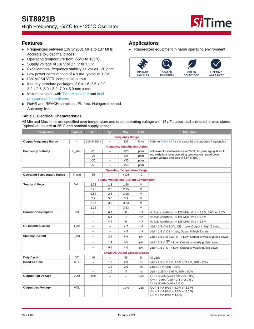
Table 1. Electrical Characteristics (continued)
Parameters Symbol Min. Typ. Max. Unit Condition
Input Characteristics
Input High Voltage VIH 70% – – Vdd Pin 1, OE or ST
Input Low Voltage VIL – – 30% Vdd Pin 1, OE or ST
Input Pull-up Impedance Z_in 50 87 150 k Pin 1, OE logic high or logic low, or ST logic high
2 – – M Pin 1, ST logic low
Startup and Resume Timing
Startup Time T_start – – 5 ms Measured from the time Vdd reaches its rated minimum value
Enable/Disable Time T_oe – – 130 ns
f = 119.342001 MHz. For other frequencies, T_oe = 100 ns + 3 * clock periods
Resume Time T_resume – – 5 ms Measured from the time ST pin crosses 50% threshold
Jitter
RMS Period Jitter T_jitt – 1.6 2.5 ps f = 125 MHz, Vdd = 2.5 V, 2.8 V, 3.0 V or 3.3 V
– 1.8 3 ps f = 125 MHz, Vdd = 1.8 V
Peak-to-peak Period Jitter T_pk – 12 20 ps f = 125 MHz, Vdd = 2.5 V, 2.8 V, 3.0 V or 3.3 V
– 14 25 ps f = 125 MHz, Vdd = 1.8 V
RMS Phase Jitter (random) T_phj – 0.5 0.8 ps f = 125 MHz, Integration bandwidth = 900 kHz to 7.5 MHz
– 1.3 2 ps f = 125 MHz, Integration bandwidth = 12 kHz to 20 MHz
Table 2. Pin Description
Pin Symbol Functionality
1 OE/ ST /NC
Output Enable H[1]: specified frequency output L: output is high impedance. Only output driver is disabled.
Standby
H[1]: specified frequency output
L: output is low (weak pull down). Device goes to sleep mode. Supply current reduces to I_std.
No Connect Any voltage between 0 and Vdd or Open[1]: Specified frequency output. Pin 1 has no function.
2 GND Power Electrical ground
3 OUT Output Oscillator output
4 VDD Power Power supply voltage[2]
Top View
1 4OE/ST/NC VDD
32GND OUT
Figure 1. Pin Assignments
Notes:
1. In OE or ST mode, a pull-up resistor of 10 kΩ or less is recommended if pin 1 is not externally driven. If pin 1 needs to be left floating, use the NC
option. 2. A capacitor of value 0.1 µF or higher between Vdd and GND is required.
SiT8921B High Frequency, -55°C to +125°C Oscillator
Rev 1.02 Page 3 of 18 www.sitime.com
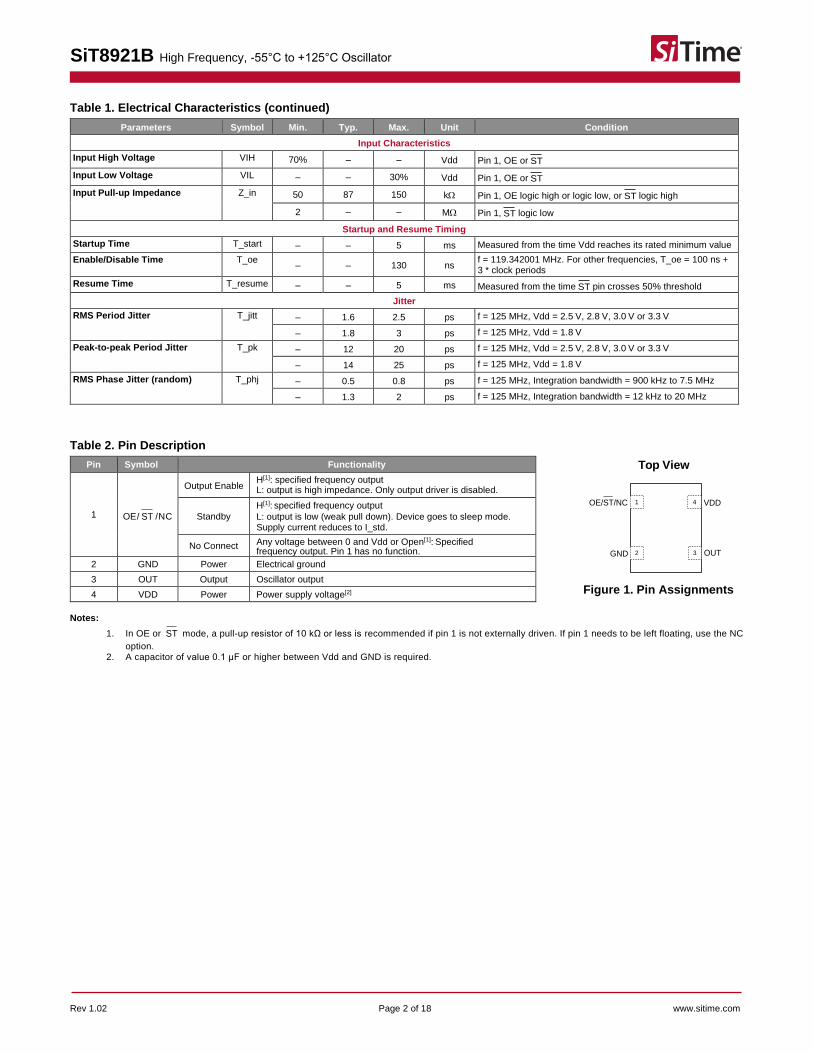
Table 3. Absolute Maximum Limits
Attempted operation outside the absolute maximum ratings of the part may cause permanent damage to the part. Actual performance of the IC is only guaranteed within the operational specifications, not at absolute maximum ratings.
Parameter Min. Max. Unit
Storage Temperature -65 150 °C
VDD -0.5 4 V
Electrostatic Discharge – 2000 V
Soldering Temperature (follow standard Pb free soldering guidelines) – 260 °C
Junction Temperature[3] – 150 °C
Note: 3. Exceeding this temperature for extended period of time may damage the device.
Table 4. Thermal Consideration[4]
Package JA, 4 Layer Board (°C/W) JA, 2 Layer Board (°C/W) JC, Bottom (°C/W)
7050 142 273 30
5032 97 199 24
3225 109 212 27
2520 117 222 26
2016 152 252 36
Note:
4. Refer to JESD51-7 for JA and JC definitions, and reference layout used to determine the JA and JC values in the above table.
Table 5. Maximum Operating Junction Temperature[5]
Max Operating Temperature (ambient) Maximum Operating Junction Temperature
125°C 135°C
Note: 5. Datasheet specifications are not guaranteed if junction temperature exceeds the maximum operating junction temperature.
Table 6. Environmental Compliance
Parameter Condition/Test Method
Mechanical Shock MIL-STD-883F, Method 2002
Mechanical Vibration MIL-STD-883F, Method 2007
Temperature Cycle JESD22, Method A104
Solderability MIL-STD-883F, Method 2003
Moisture Sensitivity Level MSL1 @ 260°C
SiT8921B High Frequency, -55°C to +125°C Oscillator
Rev 1.02 Page 4 of 18 www.sitime.com
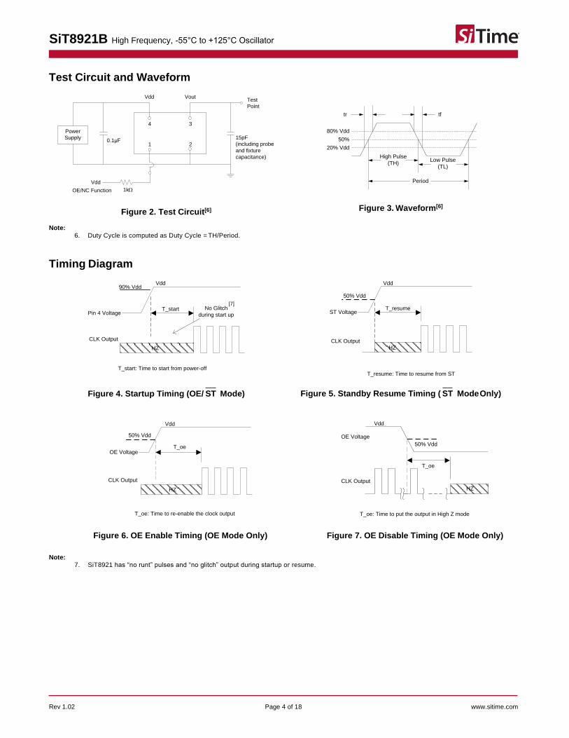
Test Circuit and Waveform
4
1
3
20.1µF
Power
Supply
OE/NC Function
Test
Point
15pF
(including probe
and fixture
capacitance)
Vdd Vout
Vdd
1k
Figure 2. Test Circuit[6]
80% Vdd
High Pulse
(TH)
50%
20% Vdd
Period
tftr
Low Pulse
(TL)
Figure 3. Waveform[6]
Note: 6. Duty Cycle is computed as Duty Cycle = TH/Period.
Timing Diagram
90% VddVdd
Pin 4 Voltage
CLK Output
T_start
T_start: Time to start from power-off
No Glitch
during start up
[7]
HZ
Figure 4. Startup Timing (OE/ ST Mode)
50% Vdd
Vdd
ST Voltage
CLK Output
T_resume
T_resume: Time to resume from ST
HZ
Figure 5. Standby Resume Timing ( ST Mode Only)
50% Vdd
Vdd
OE Voltage
CLK Output
T_oe
T_oe: Time to re-enable the clock output
HZ
Figure 6. OE Enable Timing (OE Mode Only)
50% Vdd
Vdd
OE Voltage
CLK Output
T_oe: Time to put the output in High Z mode
HZ
T_oe
Figure 7. OE Disable Timing (OE Mode Only)
Note:
7. SiT8921 has “no runt” pulses and “no glitch” output during startup or resume.
SiT8921B High Frequency, -55°C to +125°C Oscillator
Rev 1.02 Page 5 of 18 www.sitime.com
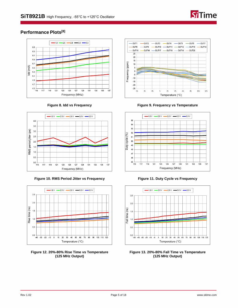
Performance Plots[8]
Figure 8. Idd vs Frequency
Figure 9. Frequency vs Temperature
Figure 10. RMS Period Jitter vs Frequency
Figure 11. Duty Cycle vs Frequency
Figure 12. 20%-80% Rise Time vs Temperature (125 MHz Output)
Figure 13. 20%-80% Fall Time vs Temperature (125 MHz Output)
SiT8921B High Frequency, -55°C to +125°C Oscillator
Rev 1.02 Page 6 of 18 www.sitime.com
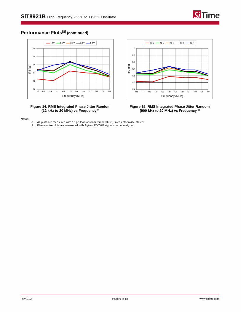
Performance Plots[8] (continued)
Figure 14. RMS Integrated Phase Jitter Random (12 kHz to 20 MHz) vs Frequency[9]
Figure 15. RMS Integrated Phase Jitter Random (900 kHz to 20 MHz) vs Frequency[9]
Notes: 8. All plots are measured with 15 pF load at room temperature, unless otherwise stated. 9. Phase noise plots are measured with Agilent E5052B signal source analyzer.
SiT8921B High Frequency, -55°C to +125°C Oscillator
Rev 1.02 Page 7 of 18 www.sitime.com
Programmable Drive Strength The SiT8921 includes a programmable drive strength feature to provide a simple, flexible tool to optimize the clock rise/fall time for specific applications. Benefits from the programmable drive strength feature are:
◼ Improves system radiated electromagnetic interference (EMI) by slowing down the clock rise/fall time
◼ Improves the downstream clock receiver’s (RX) jitter by decreasing (speeding up) the clock rise/fall time.
◼ Ability to drive large capacitive loads while maintaining full swing with sharp edge rates.
For more detailed information about rise/fall time control and drive strength selection, see the SiTime Application Notes section.
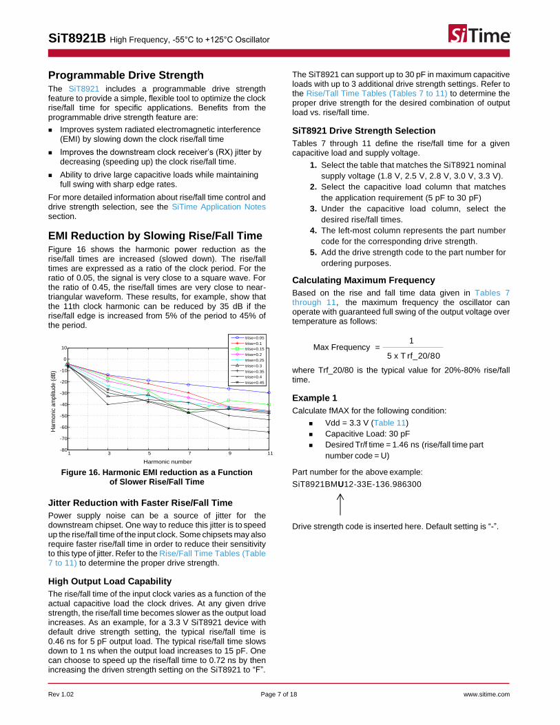
EMI Reduction by Slowing Rise/Fall Time Figure 16 shows the harmonic power reduction as the rise/fall times are increased (slowed down). The rise/fall times are expressed as a ratio of the clock period. For the ratio of 0.05, the signal is very close to a square wave. For the ratio of 0.45, the rise/fall times are very close to near-triangular waveform. These results, for example, show that the 11th clock harmonic can be reduced by 35 dB if the rise/fall edge is increased from 5% of the period to 45% of the period.
1 3 5 7 9 11-80
-70
-60
-50
-40
-30
-20
-10
0
10
Harmonic number
Ha
rmo
nic
am
plit
ud
e (
dB
)
trise=0.05
trise=0.1
trise=0.15
trise=0.2
trise=0.25
trise=0.3
trise=0.35
trise=0.4
trise=0.45
Figure 16. Harmonic EMI reduction as a Function of Slower Rise/Fall Time
Jitter Reduction with Faster Rise/Fall Time
Power supply noise can be a source of jitter for the downstream chipset. One way to reduce this jitter is to speed up the rise/fall time of the input clock. Some chipsets may also require faster rise/fall time in order to reduce their sensitivity to this type of jitter. Refer to the Rise/Fall Time Tables (Table 7 to 11) to determine the proper drive strength.
High Output Load Capability
The rise/fall time of the input clock varies as a function of the actual capacitive load the clock drives. At any given drive strength, the rise/fall time becomes slower as the output load increases. As an example, for a 3.3 V SiT8921 device with default drive strength setting, the typical rise/fall time is 0.46 ns for 5 pF output load. The typical rise/fall time slows down to 1 ns when the output load increases to 15 pF. One can choose to speed up the rise/fall time to 0.72 ns by then increasing the driven strength setting on the SiT8921 to “F”.
The SiT8921 can support up to 30 pF in maximum capacitive loads with up to 3 additional drive strength settings. Refer to the Rise/Tall Time Tables (Tables 7 to 11) to determine the proper drive strength for the desired combination of output load vs. rise/fall time.
SiT8921 Drive Strength Selection
Tables 7 through 11 define the rise/fall time for a given capacitive load and supply voltage.
1. Select the table that matches the SiT8921 nominal
supply voltage (1.8 V, 2.5 V, 2.8 V, 3.0 V, 3.3 V).
2. Select the capacitive load column that matches
the application requirement (5 pF to 30 pF)
3. Under the capacitive load column, select the
desired rise/fall times.
4. The left-most column represents the part number
code for the corresponding drive strength.
5. Add the drive strength code to the part number for
ordering purposes.
Calculating Maximum Frequency
Based on the rise and fall time data given in Tables 7 through 11, the maximum frequency the oscillator can operate with guaranteed full swing of the output voltage over temperature as follows:
where Trf_20/80 is the typical value for 20%-80% rise/fall time.
Example 1
Calculate fMAX for the following condition:
◼ Vdd = 3.3 V (Table 11)
◼ Capacitive Load: 30 pF
◼ Desired Tr/f time = 1.46 ns (rise/fall time part
number code = U)
Part number for the above example:
SiT8921BMU12-33E-136.986300
Drive strength code is inserted here. Default setting is “-”.
1
5 x T rf_20/80 = Max Frequency
SiT8921B High Frequency, -55°C to +125°C Oscillator
Rev 1.02 Page 8 of 18 www.sitime.com
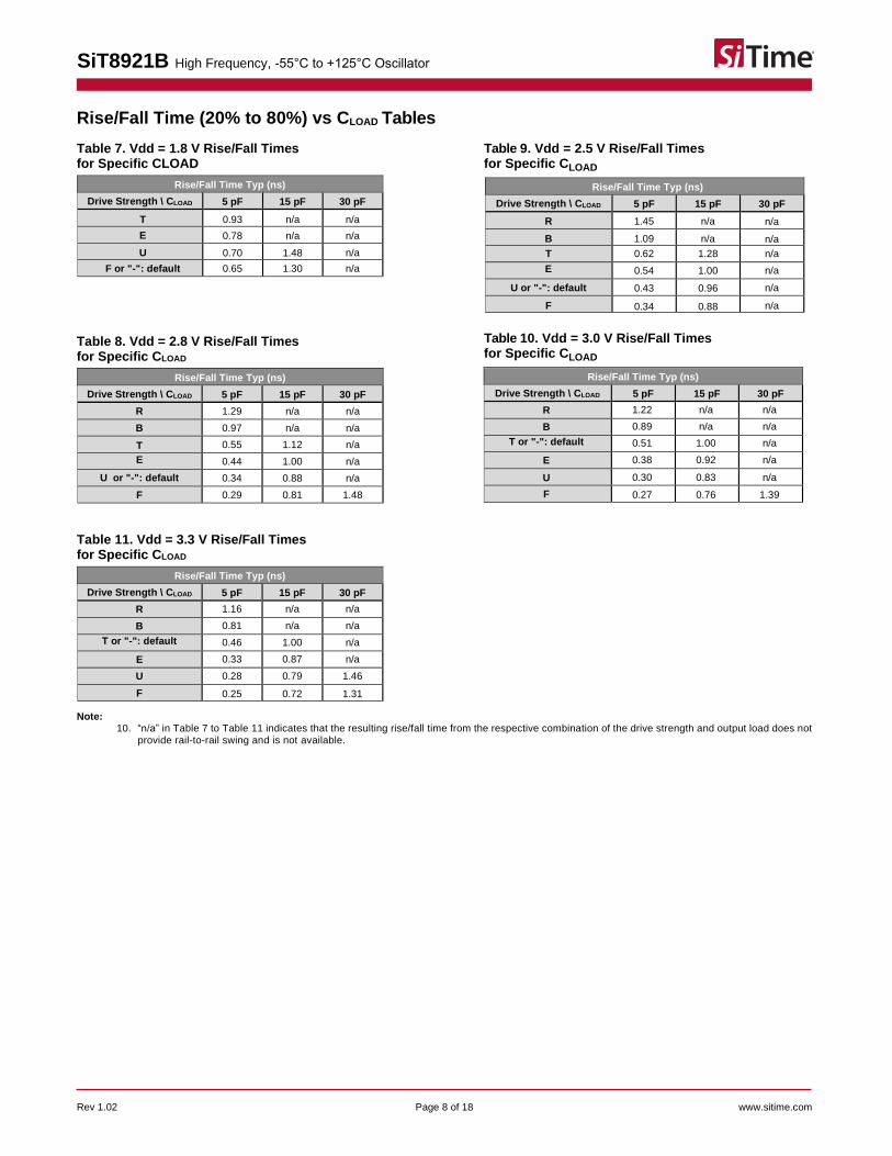
Rise/Fall Time (20% to 80%) vs CLOAD Tables
Table 7. Vdd = 1.8 V Rise/Fall Times for Specific CLOAD
Rise/Fall Time Typ (ns)
Drive Strength \ CLOAD 5 pF 15 pF 30 pF
T 0.93 n/a n/a
E 0.78 n/a n/a
U 0.70 1.48 n/a
F or "-": default 0.65 1.30 n/a
Table 8. Vdd = 2.8 V Rise/Fall Times for Specific CLOAD
Rise/Fall Time Typ (ns)
Drive Strength \ CLOAD 5 pF 15 pF 30 pF
R 1.29 n/a n/a
B 0.97 n/a n/a
T 0.55 1.12 n/a
E 0.44 1.00 n/a
U or "-": default 0.34 0.88 n/a
F 0.29 0.81 1.48
Table 9. Vdd = 2.5 V Rise/Fall Times for Specific CLOAD
Rise/Fall Time Typ (ns)
Drive Strength \ CLOAD 5 pF 15 pF 30 pF
R 1.45 n/a n/a
B 1.09 n/a n/a
T 0.62 1.28 n/a
E 0.54 1.00 n/a
U or "-": default 0.43 0.96 n/a
F 0.34 0.88 n/a
Table 10. Vdd = 3.0 V Rise/Fall Times for Specific CLOAD
Rise/Fall Time Typ (ns)
Drive Strength \ CLOAD 5 pF 15 pF 30 pF
R 1.22 n/a n/a
B 0.89 n/a n/a
T or "-": default 0.51 1.00 n/a
E 0.38 0.92 n/a
U 0.30 0.83 n/a
F 0.27 0.76 1.39
Table 11. Vdd = 3.3 V Rise/Fall Times for Specific CLOAD
Rise/Fall Time Typ (ns)
Drive Strength \ CLOAD 5 pF 15 pF 30 pF
R 1.16 n/a n/a
B 0.81 n/a n/a
T or "-": default 0.46 1.00 n/a
E 0.33 0.87 n/a
U 0.28 0.79 1.46
F 0.25 0.72 1.31
Note: 10. “n/a” in Table 7 to Table 11 indicates that the resulting rise/fall time from the respective combination of the drive strength and output load does not
provide rail-to-rail swing and is not available.
SiT8921B High Frequency, -55°C to +125°C Oscillator
Rev 1.02 Page 9 of 18 www.sitime.com
Pin 1 Configuration Options
(OE, ST , or NC)
Pin 1 of the SiT8921 can be factory-programmed to support three modes: Output enable (OE), standby (ST ̅ ̅ ̅ ) or No Connect (NC). These modes can also be programmed with the Time Machine using field programmable devices.
Output Enable (OE) Mode
In the OE mode, applying logic Low to the OE pin only disables the output driver and puts it in Hi-Z mode. The core of the device continues to operate normally. Power consumption is reduced due to the inactivity of the output. When the OE pin is pulled High, the output is typically enabled in <1 µs.
Standby ( ST ) Mode
In the ST ̅ ̅ ̅ mode, a device enters into the standby mode when Pin 1 pulled Low. All internal circuits of the device are turned off. The current is reduced to a standby current, typically in the range of a few µA. When ST ̅ ̅ ̅ is pulled High, the device goes through the “resume” process, which can take up to 5 ms.
No Connect (NC) Mode
In the NC mode, the device always operates in its normal mode and output the specified frequency regardless of the logic level on pin 1.
Table 12 below summarizes the key relevant parameters in the operation of the device in OE, ST ̅ ̅ ̅ , or NC mode.
Table 12. OE vs. ST ̅ ̅ ̅ vs. NC
OE ST NC
Active current 125 MHz (max, 1.8 V) 6 mA 6 mA 6 mA
OE disable current (max. 1.8 V) 4.5 mA N/A N/A
Standby current (typical 1.8 V) N/A 0.6 uA N/A
OE enable time at 125 MHz (max) 130 ns N/A N/A
Resume time from standby (max, all frequency) N/A 5 ms N/A
Output driver in OE disable/standby mode
High Z Weak
pull-down N/A
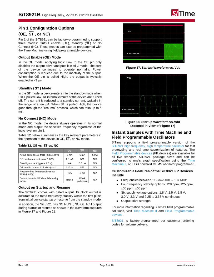
Output on Startup and Resume
The SiT8921 comes with gated output. Its clock output is accurate to the rated frequency stability within the first pulse from initial device startup or resume from the standby mode.
In addition, the SiT8921 has NO RUNT, NO GLITCH output during startup or resume as shown in the waveform captures in Figure 17 and Figure 18.
Figure 17. Startup Waveform vs. Vdd
Figure 18. Startup Waveform vs. Vdd
(Zoomed-in View of Figure 17)
Instant Samples with Time Machine and Field Programmable Oscillators SiTime supports a field programmable version of the SiT8921 high frequency, high temperature oscillator for fast prototyping and real time customization of features. The Field Programmable devices (FP devices) are available for all five standard SiT8921 package sizes and can be configured to one’s exact specification using the Time Machine II, an USB powered MEMS oscillator programmer.
Customizable Features of the SiT8921 FP Devices Include
◼ Frequencies between 119.3420001 – 137 MHz
◼ Four frequency stability options, ±20 ppm, ±25 ppm,
±30 ppm, ±50 ppm
◼ Six supply voltage options, 1.8 V, 2.5 V, 2.8 V,
3.0 V, 3.3 V and 2.25 to 3.63 V continuous
◼ Output drive strength
For more information regarding SiTime’s field programmable
solutions, visit Time Machine II and Field Programmable
devices.
SiT8921 is factory-programmed per customer ordering
codes for volume delivery.
Vdd
Clock Output
Vdd
Clock Output
SiT8921B High Frequency, -55°C to +125°C Oscillator
Rev 1.02 Page 10 of 18 www.sitime.com
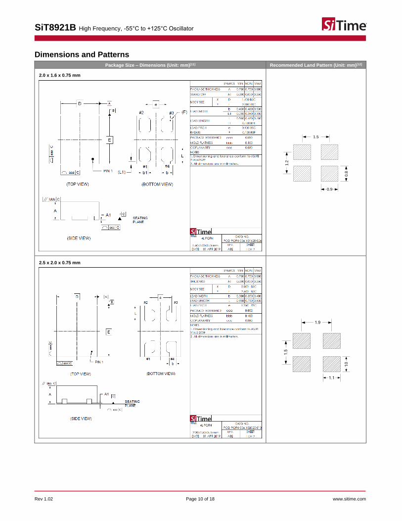
Dimensions and Patterns
Package Size – Dimensions (Unit: mm)[11] Recommended Land Pattern (Unit: mm)[12]
2.0 x 1.6 x 0.75 mm
1.5
0.8
1.2
0.9
2.5 x 2.0 x 0.75 mm
1.9
1.1
1.0
1.5
SiT8921B High Frequency, -55°C to +125°C Oscillator
Rev 1.02 Page 11 of 18 www.sitime.com
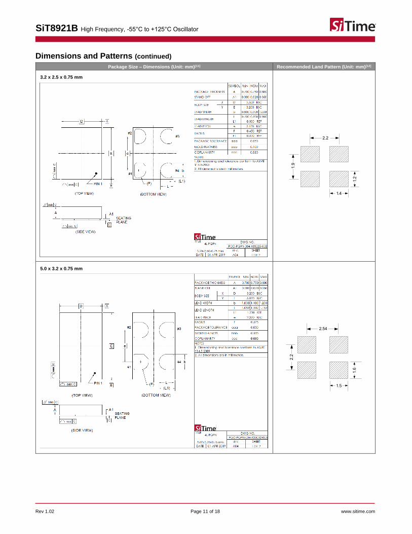
Dimensions and Patterns (continued)
Package Size – Dimensions (Unit: mm)[11] Recommended Land Pattern (Unit: mm)[12]
3.2 x 2.5 x 0.75 mm
2.2
1.9
1.4
1.2
5.0 x 3.2 x 0.75 mm
2.54
1.5
1.6
2.2

SiT8921B High Frequency, -55°C to +125°C Oscillator
Rev 1.02 Page 12 of 18 www.sitime.com
Dimensions and Patterns (continued)
Package Size – Dimensions (Unit: mm)[11] Recommended Land Pattern (Unit: mm)[12]
7.0 x 5.0 x 0.90 mm
5.08
3.8
1
2.2
2.0
Notes: 11. Top marking: Y denotes manufacturing origin and XXXX denotes manufacturing lot number. The value of “Y” will depend on the assembly location
of the device. 12. A capacitor of value 0.1 µF or higher between Vdd and GND is required.
SiT8921B High Frequency, -55°C to +125°C Oscillator
Rev 1.02 Page 13 of 18 www.sitime.com
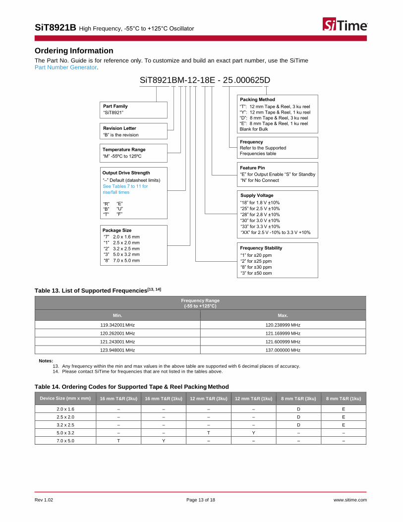
Ordering Information The Part No. Guide is for reference only. To customize and build an exact part number, use the SiTime Part Number Generator.
SiT8921BM-12-18E - 25 .000625D
Table 13. List of Supported Frequencies[13, 14]
Frequency Range
(-55 to +125°C)
Min. Max.
119.342001 MHz 120.238999 MHz
120.262001 MHz 121.169999 MHz
121.243001 MHz 121.600999 MHz
123.948001 MHz 137.000000 MHz
Notes: 13. Any frequency within the min and max values in the above table are supported with 6 decimal places of accuracy. 14. Please contact SiTime for frequencies that are not listed in the tables above.
Table 14. Ordering Codes for Supported Tape & Reel Packing Method
Device Size (mm x mm) 16 mm T&R (3ku) 16 mm T&R (1ku) 12 mm T&R (3ku) 12 mm T&R (1ku) 8 mm T&R (3ku) 8 mm T&R (1ku)
2.0 x 1.6 – – – – D E
2.5 x 2.0 – – – – D E
3.2 x 2.5 – – – – D E
5.0 x 3.2 – – T Y – –
7.0 x 5.0 T Y – – – –
l
S
SiT8921B High Frequency, -55°C to +125°C Oscillator
Rev 1.02 Page 14 of 18 www.sitime.com
Table 15. Additional Information
Document Description Download Link
Time Machine II MEMS oscillator programmer http://www.sitime.com/support/time-machine-oscillator-programmer
Field Programmable
Oscillators Devices that can be programmable in the field by Time Machine II
http://www.sitime.com/products/field-programmable-oscillators
Manufacturing Notes Tape & Reel dimension, reflow profile and other manufacturing related info
https://www.sitime.com/sites/default/files/gated/Manufacturing-Notes-for-SiTime-Products.pdf
Qualification Reports RoHS report, reliability reports, composition reports
http://www.sitime.com/support/quality-and-reliability
Performance Reports Additional performance data such as phase noise, current consumption and jitter for selected frequencies
http://www.sitime.com/support/performance-measurement-report
Termination Techniques Termination design recommendations http://www.sitime.com/support/application-notes
Layout Techniques Layout recommendations http://www.sitime.com/support/application-notes
Table 16. Revision History
Version Release Date Change Summary
1.0 7-May-2015 Final production release
1.01 2-Jan-2017 Added 16 mm T&R information to Table 14 Revised 12 mm T&R information to Table 14
1.02 15-Jun-2021 Updated logo and company address, other page layout changes Updated Dimensions and Patterns package drawings
SiTime Corporation, 5451 Patrick Henry Drive, Santa Clara, CA 95054, USA | Phone: +1-408-328-4400 | Fax: +1-408-328-4439
© SiTime Corporation 2015-2021. The information contained herein is subject to change at any time without notice. SiTime assumes no responsibility or liabi lity for any loss, damage or defect of a Product which is caused in whole or in part by (i) use of any circuitry other than circuitry embodied in a SiTime product, (ii) misuse or abuse including static discharge, neglect or accident, (iii) unauthorized modification or repairs which have been soldered or altered during assembly and are not capable of being tested by SiTime under its normal test conditions, or (iv) improper installation, storage, handling, warehousing or transportation, or (v) being subjected to unusual physical, thermal, or electrical stress. Disclaimer: SiTime makes no warranty of any kind, express or implied, with regard to this material, and specifically disclaims any and all express or implied warranties, either in fact or by operation of law, statutory or otherwise, including the implied warranties of merchantability and fitness for use or a particular purpose, and any implied warranty arising from course of dealing or usage of trade, as well as any common-law duties relating to accuracy or lack of negligence, with respect to this material, any SiTime product and any product documentation. Products sold by SiTime are not suitable or intended to be used in a life support application or component, to operate nuclear facilities, or in other mission critical applications where human life may be involved or at stake. All sales are made conditioned upon compliance with the critical uses policy set forth below. CRITICAL USE EXCLUSION POLICY
BUYER AGREES NOT TO USE SITIME'S PRODUCTS FOR ANY APPLICATION OR IN ANY COMPONENTS USED IN LIFE SUPPORT DEVICES OR TO OPERATE NUCLEAR FACILITIES OR FOR USE IN OTHER MISSION-CRITICAL APPLICATIONS OR COMPONENTS WHERE HUMAN LIFE OR PROPERTY MAY BE AT STAKE. SiTime owns all rights, title and interest to the intellectual property related to SiTime's products, including any software, firmware, copyright, patent, or trademark. The sale of SiTime products does not convey or imply any license under patent or other rights. SiTime retains the copyright and trademark rights in all documents, catalogs and plans supplied pursuant to or ancillary to the sale of products or services by SiTime. Unless otherwise agreed to in writing by SiTime, any reproduction, modification, translation, compilation, or representation of this material shall be strictly prohibited.
Silicon MEMS Outperforms Quartz
Rev 1.02 Page 15 of 18 www.sitime.com
Supplemental Information
The Supplemental Information section is not part of the datasheet and is for informational purposes only.
Silicon MEMS Outperforms Quartz
Rev 1.02 Page 16 of 18 www.sitime.com
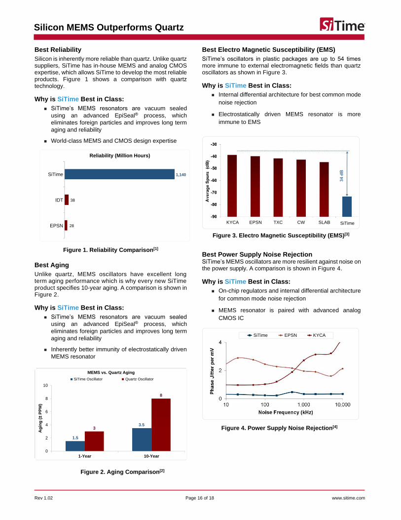
Best Reliability
Silicon is inherently more reliable than quartz. Unlike quartz suppliers, SiTime has in-house MEMS and analog CMOS expertise, which allows SiTime to develop the most reliable products. Figure 1 shows a comparison with quartz technology.
Why is SiTime Best in Class:
◼ SiTime’s MEMS resonators are vacuum sealed
using an advanced EpiSeal® process, which
eliminates foreign particles and improves long term
aging and reliability
◼ World-class MEMS and CMOS design expertise
EPSN
IDT
SiTime
28
38
1,140
Reliability (Million Hours)
Figure 1. Reliability Comparison[1]
Best Aging
Unlike quartz, MEMS oscillators have excellent long term aging performance which is why every new SiTime product specifies 10-year aging. A comparison is shown in Figure 2.
Why is SiTime Best in Class:
◼ SiTime’s MEMS resonators are vacuum sealed
using an advanced EpiSeal® process, which
eliminates foreign particles and improves long term
aging and reliability
◼ Inherently better immunity of electrostatically driven
MEMS resonator
1.5
3.53
8
0
2
4
6
8
10
1-Year 10-Year
Ag
ing
(
PP
M)
MEMS vs. Quartz Aging
EpiSeal MEMS Oscillator Quartz OscillatorQuartz Oscillator
1.5
3.5
SiTime Oscillator
Figure 2. Aging Comparison[2]
Best Electro Magnetic Susceptibility (EMS)
SiTime’s oscillators in plastic packages are up to 54 times more immune to external electromagnetic fields than quartz oscillators as shown in Figure 3.
Why is SiTime Best in Class:
◼ Internal differential architecture for best common mode
noise rejection
◼ Electrostatically driven MEMS resonator is more
immune to EMS
SiTimeSLABKYCA CWEPSN TXC
Figure 3. Electro Magnetic Susceptibility (EMS)[3]
Best Power Supply Noise Rejection SiTime’s MEMS oscillators are more resilient against noise on the power supply. A comparison is shown in Figure 4.
Why is SiTime Best in Class:
◼ On-chip regulators and internal differential architecture
for common mode noise rejection
◼ MEMS resonator is paired with advanced analog
CMOS IC
SiTime KYCAEPSN
Figure 4. Power Supply Noise Rejection[4]
Silicon MEMS Outperforms Quartz
Rev 1.02 Page 17 of 18 www.sitime.com
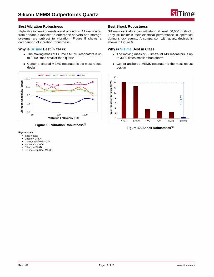
Best Vibration Robustness
High-vibration environments are all around us. All electronics, from handheld devices to enterprise servers and storage systems are subject to vibration. Figure 5 shows a comparison of vibration robustness.
Why is SiTime Best in Class:
◼ The moving mass of SiTime’s MEMS resonators is up
to 3000 times smaller than quartz
◼ Center-anchored MEMS resonator is the most robust
design
0.0
0.1
1.0
10.0
100.0
10 100 1000
Vib
rati
on
Sen
sit
ivit
y (
pp
b/g
)
Vibration Frequency (Hz)
TXC EPS CW KYCA SLAB EpiSeal MEMSSiTimeSLABKYCACWEPSTXC
Figure 16. Vibration Robustness[5]
Figure labels:
▪ TXC = TXC ▪ Epson = EPSN ▪ Connor Winfield = CW ▪ Kyocera = KYCA ▪ SiLabs = SLAB ▪ SiTime = EpiSeal MEMS
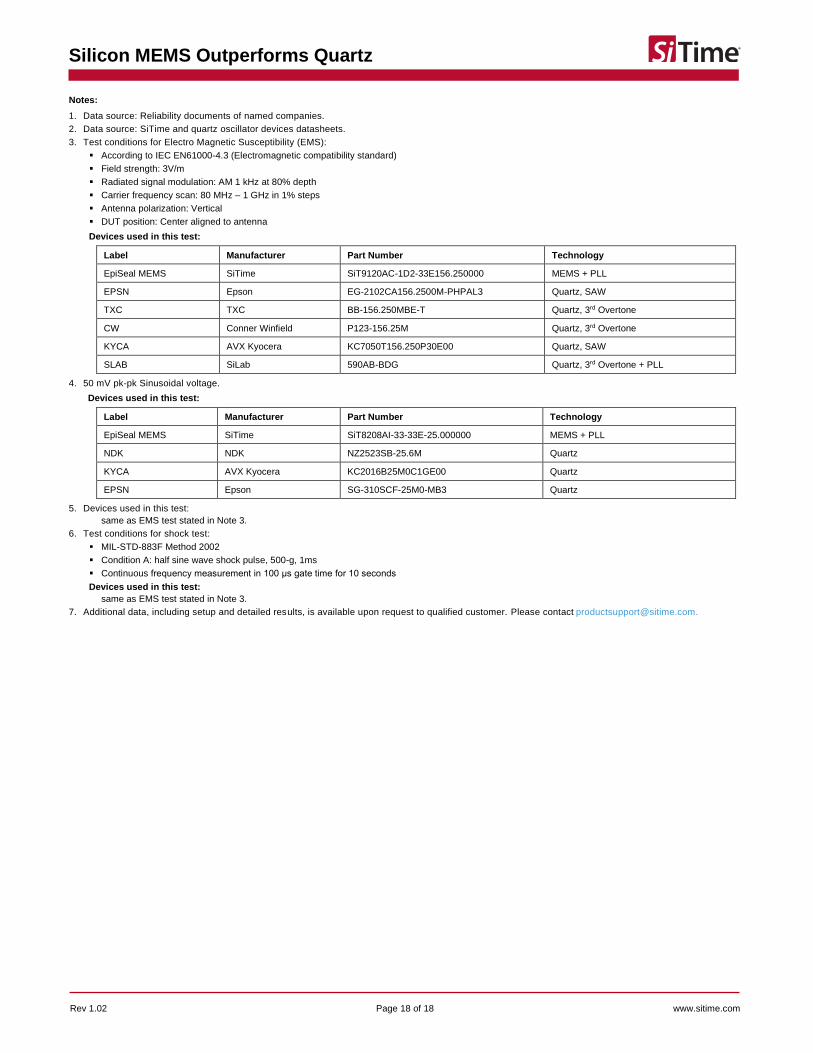
Best Shock Robustness
SiTime’s oscillators can withstand at least 50,000 g shock. They all maintain their electrical performance in operation during shock events. A comparison with quartz devices is shown in Figure 6.
Why is SiTime Best in Class:
◼ The moving mass of SiTime’s MEMS resonators is up
to 3000 times smaller than quartz
◼ Center-anchored MEMS resonator is the most robust
design
SiTimeSLABKYCA CWEPSN TXC
Figure 17. Shock Robustness[6]
Silicon MEMS Outperforms Quartz
Rev 1.02 Page 18 of 18 www.sitime.com
Notes:
1. Data source: Reliability documents of named companies.
2. Data source: SiTime and quartz oscillator devices datasheets.
3. Test conditions for Electro Magnetic Susceptibility (EMS):
▪ According to IEC EN61000-4.3 (Electromagnetic compatibility standard)
▪ Field strength: 3V/m
▪ Radiated signal modulation: AM 1 kHz at 80% depth
▪ Carrier frequency scan: 80 MHz – 1 GHz in 1% steps
▪ Antenna polarization: Vertical
▪ DUT position: Center aligned to antenna
Devices used in this test:
Label Manufacturer Part Number Technology
EpiSeal MEMS SiTime SiT9120AC-1D2-33E156.250000 MEMS + PLL
EPSN Epson EG-2102CA156.2500M-PHPAL3 Quartz, SAW
TXC TXC BB-156.250MBE-T Quartz, 3rd Overtone
CW Conner Winfield P123-156.25M Quartz, 3rd Overtone
KYCA AVX Kyocera KC7050T156.250P30E00 Quartz, SAW
SLAB SiLab 590AB-BDG Quartz, 3rd Overtone + PLL
4. 50 mV pk-pk Sinusoidal voltage.
Devices used in this test:
Label Manufacturer Part Number Technology
EpiSeal MEMS SiTime SiT8208AI-33-33E-25.000000 MEMS + PLL
NDK NDK NZ2523SB-25.6M Quartz
KYCA AVX Kyocera KC2016B25M0C1GE00 Quartz
EPSN Epson SG-310SCF-25M0-MB3 Quartz
5. Devices used in this test:
same as EMS test stated in Note 3.
6. Test conditions for shock test:
▪ MIL-STD-883F Method 2002
▪ Condition A: half sine wave shock pulse, 500-g, 1ms
▪ Continuous frequency measurement in 100 μs gate time for 10 seconds
Devices used in this test:
same as EMS test stated in Note 3.
7. Additional data, including setup and detailed results, is available upon request to qualified customer. Please contact [email protected].