Embed Size (px)
Citation preview

1
Abstract— Renewable energies have become increasingly more
relevant considering the fossil fuels shortage and the fact of being
eco-friendly, with no waste emissions. Photovoltaics, in particular,
has been one of the most required renewable energy, more and
more accessible to the general public, available for self-
-consumption and self-production.
This thesis will be focused on the analysis and design of a single
phase DC-AC converter, often called inverter, using input voltage
and output current control methodologies. Therefore the DC-AC
converter assumes an important role in the photovoltaic to grid
power transmitting process.
The implemented topology consists on a H4 full bridge inverter
since this is the topology that offers the best trade-off between
efficiency and cost. The last advantages have been widely studied
with positive results in several practical applications. The inverter
output current control was assured by a nonlinear control
methodology combined with frequency limiting block, in
alternative to the use of the most popular hysteretic methodologies.
On the other hand the input voltage control consists on a
proportional integral linear compensator, assuring steady-state
zero error performance.
Keywords — Full-Bridge Inverter, DC-AC Converter, Power
Electric Converter, Inverter Control, Photovoltaic System, 3 Level
PWM
I. INTRODUCTION
HE implemented DC-AC converter is part of a photovoltaic
system with two stages of power conversion. According to
figure 1, this is composed by photovoltaic panels, followed by
a DC-DC converter, culminating in a DC-AC converter, also
designated as inverter.
PV Grid
DC-AC Converter
(Inverter)DC-DC ConverterLR
DC
DC
DC
AC
CBCA
Figure 1 – Implemented photovoltaic-system topology
To connect the inverter to the electrical grid a inductor is
used. Between the DC-DC and DC-AC converters there is a
capacitor responsible for keeping a constant voltage in the input
inverter terminals.
The capacitor between the photovoltaic panels and the DC-
DC converter is used to decouple the inverter alternate
component.
In this topology, the continuous voltage imposed by the
photovoltaic panel is applied in the DC-DC converter input. CA
capacitor’s aim is to filter the ripple component of the DC-DC
converter input voltage, which will ideally make the panel to
see only the average value. As the DC-DC converter output
voltage is intended to be higher than the panel’s, this last
converter should be a boost. The established value for the DC-
DC converter output voltage should be as continuous as
possible, with CB reducing the voltage ripple.
II. SINGLE-PHASE INVERTER
The topology of the block relative to the DC-AC converter
will be responsible for converting input continuous power into
alternate power to be injected in the grid. The type of inverter
to be used is the full-bridge, H4 type, as this project aims at
implementing an inverter with high efficiency, reliability and
low cost. The schematic of the implemented topology is
presented in figure 2.
VC
PV Panels
+
DC-DC
Converter
iC
InverterDC-Link
C
T1 T2
T3T4
D2
D3
D1
D4
vAB
A
B
vRede
LRiR
S4S3
S2S1
Figure 2 – DC-AC Converter (H4 inverter)
The block defined by the dashed line let us look through the
DC-AC converter, this study’s object and the 1st order filter
composed by a LR inductor making the coupling between the
grid and the voltage to the inverter terminals.
Single-Phase Inverter for Photovoltaic Panels
with Voltage and Current Control
Filipe Carlos de Oliveira Simões
Instituto de Telecomunicações, Instituto Superior Técnico, 1049-001 Lisboa, Portugal
E-mail: [email protected]
T

2
III. CONTINUOUS CONDUCTION MODE
When analysing the inverter in figure 2, all its constituent
components are taken into account, that is, the T1, T2, T3 and T4
semiconductors, as well as the respective diodes in anti-parallel.
Each group formed by a transistor and the respective diode is
designated as S1, S2, S3 and S4 (switches), respectively. C
capacitor, in the input, may be put close, in a simplified manner
to a continuous voltage source, as the previous stage guarantees
that voltage.
Knowing whether to use a three level sinusoidal pulse with
modulation, the inverter output voltage, vAB, may have three
different values: +VC, zero e –VC. Therefore, the converter
functioning may be as:
𝛾1 = { 1 𝑠𝑒 𝑆1𝑂𝑁 𝑒 𝑆4𝑂𝐹𝐹
0 𝑠𝑒 𝑆4𝑂𝑁 𝑒 𝑆1𝑂𝐹𝐹 , (1)
and
𝛾2 = { 1 𝑠𝑒 𝑆2𝑂𝑁 𝑒 𝑆3𝑂𝐹𝐹
0 𝑠𝑒 𝑆3𝑂𝑁 𝑒 𝑆2𝑂𝐹𝐹 . (2)
From the expression giving the voltage between the two arms
of the inverter, vAB, is as it follows;
𝑣𝐴𝐵 = 𝑉𝐶 (𝛾1 − 𝛾2), (3)
the four possible functioning states for a three-level modulation
are obtained, presented in table 1.
Table 1- Operating states of the semiconductor full- bridge inverter
Name States S1 S2 S3 S4 vAB
S10 𝛾1 = 1 𝛾2 = 0 ON OFF ON OFF +VC
S00 𝛾1 = 0 𝛾2 = 0 OFF OFF ON ON 0
S11 𝛾1 = 1 𝛾2 = 1 ON ON OFF OFF 0
S01 𝛾1 = 0 𝛾2 = 1 OFF ON OFF ON +VC
The behaviour of the circuit variables for each commutation
state of semiconductors is described in table 2.
Table 2 - Behavior of the circuit variables in the various switching states
𝜸𝟏 𝜸𝟐 vAB vRede vLR 𝒅𝒊𝑳𝑹𝒅𝒕
0 0 0 0 0
0 1 -VC 0 0
1 0 +VC 0 0
1 1 0 0 0
0 0 0 0 0
0 1 -VC 0 0
1 0 +VC 0 0
1 1 0 0 0
IV. CONVERTER DESIGN
The implemented inverter was sized according to the
following parameters:
Table 3 - Values for the design of the inverter
Pmáx - Maximum power 15W
VC - Inverter input voltage 30V
VRedeRMS - Effective grid voltage 17,25V
fRede - Grid frequency 50Hz
iR – Current in LR inductor 0,87A
∆iR – Current ripple in LR inductor
bobina LR
5%
A) LR inductor sizing
Getting started by dimensioning the LR inductor, it is known
that differential equation that defines the voltage variation in
the inductor over time is given by:
𝑣𝐿𝑅(𝑡) = 𝐿𝑅𝑑𝑖𝑅 (𝑡)
𝑑𝑡 , (4)
where,
𝑖𝑅(𝑡) = √2 ⋅ 𝐼𝑒𝑓 ⋅ sin (2𝜋𝑓𝑡 + 𝜑) , (5)
deriving the expression (4), obtains the final expression for 𝑣𝐿𝑅,
shown in (5):
𝑣𝐿𝑅(𝑡) = 𝐿𝑅 ⋅ √2 ⋅ 𝑖𝑅 𝑒𝑓 ⋅ cos(𝜔𝑡 + 𝜑) ⋅ 𝜔 (6)
Knowing in advance that the inverter voltage is equal to the
voltage on the input capacitor, VC, or the symmetrical of this, or
zero, it is concluded that the value of 𝑣𝐴𝐵 in the inverter output,
in any moment, it can never exceed the interval [+VC, -VC].
Therefore there is the need to limit the LR voltage of the
inductor, since it takes very high values, with an equally high
voltage drop. This voltage drop, when added to the grid voltage
may lead to higher values of vAB voltage, higher than the voltage
at the input capacitor, which is not possible.
Doing the opposite analysis, it is intended to know the
voltage of the inverter, vAB, for a given value of LR. The value of
LR must be such that fulfills the vAB value range defined in the
expression (7).
Therefore, under this assumption, it can obtain the optimal
inductor value having regard to the following expressions:
𝑣𝐴𝐵[ − 𝑉𝐶 , +𝑉𝐶] (7)
𝑣𝐴𝐵 = 𝑣𝐿𝑅 + 𝑣𝑟𝑒𝑑𝑒 (8)
where,
𝑣𝑟𝑒𝑑𝑒(𝑡) = √2 ⋅ 𝑉𝑒𝑓 ⋅ sin (2𝜋𝑓𝑡 + 𝜑) (9)
then,
𝑣𝐴𝐵 = [𝐿𝑅 ⋅ √2 ⋅ 𝑖𝑅 𝑒𝑓 ⋅ cos(𝜔𝑡) ⋅ 𝜔 + √2 ⋅ 𝑉𝑒𝑓 ⋅ sin (2𝜋𝑓𝑡)] (10)
Thus, starting from equation (10), the voltage was simulated
for various values of LR, having reached the value LR=44mH.

3
Having scaled the inductor, it was calculated the frequency
inverter switching. From differential equation that defines the
voltage variation in the inductor over time given by equation
(4), it is possible to linearize the ripple of current to high
frequencies, by straight sections being rewritten by:
∆𝑖𝑅
∆𝑇𝑆=
𝑣𝐿𝑅
𝐿𝑅 (11)
𝑇𝑆 can then be calculated taking into account a certain current
ripple set based on 𝑖𝑟𝑚á𝑥, being current at the inverter output
for maximum power.
The ripple obtained by the current iR, shown in figure 3, is
essentially defined based on the slope of the current in order to
time.
TS
iR
Figure 3 –Ripple definition
Based on the current setting of the ripple in the inductor, and
using the expression (11) can be obtained the equation for
calculating 𝑇𝑆.
∆𝑇𝑆 =𝐿𝑅⋅∆𝑖𝑅𝑚á𝑥
𝑣𝐿𝑅𝑚á𝑥 , (12)
where 𝑣𝐿𝑅𝑚á𝑥, must be set based on the maximum potential
difference that can be observed to ensure the sizing of the
inductor for the worst case.
Analyzing the scheme in figure 4, it can be seen that the
inverter voltage 𝑣𝐴𝐵 , can take the values +VC, -VC or zero, for
the case of three-level PWM. On the other hand, the grid can
take maximum values in the range [-24,4V to +24,4V].
VC
VC
0
+VC
-VC
vRede
LRiR
vAB
vLR
Figure 4 - Scheme that defines the variation voltage to the inductor terminals
However, since the circuit consists of an inductive load, there
is a mismatch between 𝑣𝐴𝐵 voltage and the 𝑣𝑟𝑒𝑑𝑒 voltage,
whereby there will be times when the 𝑣𝐿𝑅 voltage drop will be
higher than 30V. What happens in this particular case can be
described by the content of the figure 5.
vRede 14V
LRiR
vLRmáx 44VvAB = 30V
Figure 5 - Scheme which defines the worst case voltage to the inductor
terminals LR
The result of the voltage waveform vRede with the vAB voltage
waveform, allows to obtain the waveform of the real vLR,
voltage shown in figure 6, from which can be take the maximum
voltage peak.
Figure 6 - Real vLR voltage with the maximum voltage point
Withdraws from the figure 6 the maximum point value,
𝑣𝐿𝑅𝑚á𝑥 ≈ 44V. this voltage being given analytically by:
𝑣𝐿𝑅𝑚á𝑥 = 𝑣𝐴𝐵 − 𝑣𝑟𝑒𝑑𝑒 (13)
𝑣𝐿𝑅𝑚á𝑥 = 30 − (−14) ≅ 44𝑉 (14)
B) Switching frequency sizing
From this analysis it is possible to calculate the inverter
switching frequency, remaining only set the ripple current
𝑖𝑅𝑚á𝑥 to be considered.
In that case, it is considered a ripple of 5% of the current
𝑖𝑅𝑚á𝑥= √2 ×0,87A and as such, based on the equation (12)
results in:
∆𝑇𝑆 =(45×10−3) ×(0,05 ×0,87× √2)
44≅ 62,9µ𝑠 (15)
The inverter switching frequency is given by:
𝑓𝑆 = 1
𝑇𝑆= 15,9𝑘𝐻𝑧, (16)
C) C capacitor sizing
Starting from the scheme on figure 7 can begin to analyze the
variables affecting the input capacitor behavior of the inverter,
which ensures low voltage ripple.
DC
AC
DC-AC Converter
(Inverter)LR
ppainel pin prede
PV Panels
+
DC-DC
ConverterC
iD ii
iC
vRede
Figure 7 - Scheme for sizing the capacitor C
The power from the photovoltaic panels is defined as ppainel
and the power in the inverter input is defined as pin. pC is the
capacitor instantaneous power given by the expression (17)
𝑝𝐶 = 𝑝𝑝𝑎𝑖𝑛𝑒𝑙 − 𝑝𝑖𝑛 (17)
where ppainel may be approximately continuous and equal to the
average value of the Prede=<prede> power, considering the

4
system’s efficiency is close to the unit. On the other hand, pin
will correspond to the instantaneous power in the grid, prede, as
in the DC-AC converter there is no element to store energy.
For a given grid voltage, in phase with voltage, with an
effective IR, obtains:
𝑃𝑟𝑒𝑑𝑒 = 𝑉𝑅 ⋅ 𝐼𝑅 ⋅ cos (0) (18)
The instantaneous power of the AC side, prede, will then be
described according to the product between the voltage and the
grid voltage:
𝑝𝑟𝑒𝑑𝑒(𝑡) = 𝑣𝑟𝑒𝑑𝑒(𝑡) ⋅ 𝑖𝑟𝑒𝑑𝑒(𝑡) (19)
Knowing that the capacitor instantaneous power, pcondensador,
is given by:
𝑝𝐶(𝑡) = 𝑣𝑐(𝑡) ⋅ 𝑖𝑐(𝑡) = 𝐶 ⋅ 𝑣𝑐(𝑡)𝑑𝑣𝐶(𝑡)
𝑑𝑡 (20)
From equation (20), it is possible to develop it using the
special case described by (21):
𝑓(𝑡) = 𝑘 ⋅ 𝑥(𝑡)𝑑𝑥(𝑡)
𝑑𝑡 . (21)
Solving in terms of x and replacing the required variables can
get:
𝑣𝐶(𝑡) = √𝑘𝑎 ∫ 𝑝𝐶(𝑡) 𝑑𝑡 + 𝑡
0𝑘𝑏 , (22)
To calculate the 𝑘𝑎, values it is used the relation defined by
the equation (22), to rewrite the expression (20), getting:
𝑝𝐶(𝑡) = 𝐶√𝑘𝑎 ∫ 𝑝𝐶(𝑡) 𝑑𝑡 + 𝑡
0𝑘𝑏 ⋅
𝑘𝑎.𝑝𝐶(𝑡)
2√𝑘𝑎 ∫ 𝑝𝐶(𝑡) 𝑑𝑡+ 𝑡0 𝑘𝑏
, (23)
Solving in terms of 𝑘𝑎, can get:
𝑘𝑎 =2
𝐶 , (24)
To get the 𝑘𝑏, it is used the expression (22) to t = 0, getting:
𝑘𝑏 = 𝑣𝐶(0)2 (25)
From the equations defined in (18) and (19) results:
𝑝𝐶(𝑡) = 𝑃𝑟𝑒𝑑𝑒 − 𝑝𝑟𝑒𝑑𝑒(𝑡)
𝑝𝐶(𝑡) = 𝑉𝑒𝑓 . 𝐼𝑒𝑓 . sin (2𝜔𝑡) (26)
By integrating both parts of (26) obtains:
∫ 𝑝𝐶 𝑑𝑡𝑡
0= ∫ 𝑉𝑒𝑓 ⋅ 𝐼𝑒𝑓 ⋅ sin (2𝜔𝑡)
𝑡
0 𝑑𝑡 =
𝑉𝑒𝑓⋅𝐼𝑒𝑓⋅−cos (2𝜔𝑡)
2𝜔 (27)
By using the expression (22), the capacitor voltage will be
given by:
𝑣𝐶(𝑡) = √2
𝐶
𝑉𝑒𝑓⋅𝐼𝑒𝑓⋅(− cos(2𝜔𝑡))
2𝜔+ 𝑣𝐶(0)
2 (28)
Through equation (23) it was possible to calculate the
capacitor value which leads to a 𝑣𝐶 ripple equal to 4% of the
maximum value of that voltage (∆𝑣𝐶 = 4%).
The C value suiting that requirement is C = 660F .
V. INVERTER CONTROL
It is necessary to control the following variables in the
inverter:
Voltage in C capacitor, named VC, ensuring the energetic
balance of the circuit and keeping a constant voltage in the
capacitor.
Current injected in the grid, named iR, allowing the control of
the power to be injected in the grid.
The full schematic of the control system to be implemented
in the studied converter is shown in figure 8.
DC
AC
DC-AC Converter
(Inverter)LR
PV Panels
+
DC-DC
ConverterC
iD ii
iC
VC
T1 T2 T3 T4
γ1 γ2
iR
Gain αv
vC voltage
controlo
iR current
control
sin(ωt)
-
+PI
iRiRref
VCref
vRede
Figure 8 - Schematic converter control system
Figure 9 shows the blocks diagram in Matlab of the
implemented control.
Figure 9 –Inverter’s block diagram in Matlab
The “Inverter” block was implemented in Matlab based on
its model study, coming up to the equations ruling its
functioning, as:
𝑣𝐴 = 𝛾1 ⋅ 𝑉𝐶 𝑣𝐵 = 𝛾2 ⋅ 𝑉𝐶 (29)
Thus, vAB is represented by:
𝑣𝐴𝐵 = 𝑣𝐴 − 𝑣𝐵 = 𝑉𝐶(𝛾1 − 𝛾2) (30)

5
the equation ruling the inverter model. To simulate the circuit
currents it was necessary to determine the equation leading to
the definition of the ii inverter input current, which is obtained
by analysing the currents in each diode plus transistor cells.
𝑖𝑆1 = { 𝑖𝑅 𝑠𝑒 𝛾1 = 1
0 𝑠𝑒 𝛾1= 0
𝑖𝑆4 = {−𝑖𝑅 𝑠𝑒 𝛾1 = 0
0 𝑠𝑒 𝛾1= 1
(31)
𝑖𝑆2 = {−𝑖𝑅 𝑠𝑒 𝛾2 = 1
0 𝑠𝑒 𝛾2= 0
𝑖𝑆3 = { 𝑖𝑅 𝑠𝑒 𝛾2 = 0
0 𝑠𝑒 𝛾2= 1
(32)
The input current is, then, given by:
𝑖𝑖 = 𝑖𝑆1 + 𝑖𝑆2 = 𝑖𝑆3 + 𝑖𝑆4 = 𝑖𝑅( 𝛾1 − 𝛾2) (33)
Figure 10 illustrates the inverter block diagram in Matlab.
Figure 10 – Inverter’s block diagram (see equation (32))
A) iR current control
In this study it is used a nonlinear control with a frequency
limitation to control iR current. This control system in based on
the following criteria:
If the iR current iRref, then vLR must be 0, in so much that
the iR current must increase,
If the iR current iRref, then vLR must be 0, so much that the
iR current must diminish.
From figure 11 where the operation areas are presented as
well as the comparison limits, it is known, a priori, the error is
given by:
𝑒𝑟𝑟𝑜𝑟 = 𝑖𝑅𝑟𝑒𝑓 − 𝑖𝑅 (34)
With iRref as the reference current and iR the real circuit output
current, being the first a sinusoidal wave without ripple, the
second, due to the discrete character of the inverter voltage,
assumes a line sections behavior associated to a given ripple,
with a sinusoidal form.
Thus, the error will come out as a result from the subtraction
of the iRref waveform to the iR waveform, as shown in figure 11,
where the operation areas and the comparison limits are also
presented.
errormáx
ZA
errormin
error
ZB
ZC
ZA
0
Figure 11 – Waveform of the error, comparing the different error zones
It may be assumed that the three control functioning areas
are given by:
𝐴 𝑍𝑜𝑛𝑒 𝑒𝑟𝑟𝑜𝑟 𝑒𝑟𝑟𝑜𝑟𝑚á𝑥 𝑣𝐴𝐵 = +𝑉𝐶 (35)
𝐶 𝑍𝑜𝑛𝑒 𝑒𝑟𝑟𝑜𝑟 𝑒𝑟𝑟𝑜𝑟𝑚𝑖𝑛 𝑣𝐴𝐵 = −𝑉𝐶 (36)
𝐵 𝑍𝑜𝑛𝑒 𝑒𝑟𝑟𝑜𝑟𝑚𝑖𝑛 𝑒𝑟𝑟𝑜𝑟 𝑒𝑟𝑟𝑜𝑟𝑚á𝑥 𝑣𝐴𝐵 = 0 (37)
To better understand the responsible circuit for the output
power control, the corresponding blocks diagram in Matlab is
presented in figure 12.
Figure 12 – Block diagram of the non-linear control circuit with frequency
limitation
The error is then compared with the defined errormáx and
errormin, reaching the signals entering the logical table,
responsible for defining the 𝛾1and 𝛾2 states.
The g1 and g2 flip-flops connected to the logical table exit
have the function of limiting the commutation frequency. The
flip-flop flag will cause, in the inverter free-wheel states (S00 e
S11), alternation between the superior and inferior
semiconductors of each arm, ensuring the semiconductors
balance to conduction. The states alternation is updated by the
output of the XNOR gate used, which detects the S00 and S11
states. The use of this logical gate comes from the analysis of
table 4. Table 4 – Truth table of the implemented logical circuit
C1 C2 Flag 𝟏 𝟐 VAB
0 0 0
0 0
0 0 1
0 1 N.A 0 1 -VC
1 0 N.A 1 0 +VC
1 1 N.A N.A. N.A. N.A.
Where the C1 and C2signals correspond to the comparators
used. The corresponding equations to each gamma variable may

6
be found, which allows to find the logical circuit implementing
the required function.
1= C1. C2̅̅̅̅ + C1̅̅̅̅ . C2̅̅̅̅ . 𝐹𝑙𝑎𝑔 (38)
2= C1̅̅̅̅ . C2 + C1̅̅̅̅ . C2̅̅̅̅ . 𝐹𝑙𝑎𝑔 (39)
The logical circuit which allows controlling the transistors is
then implemented, preventing the simultaneous conduction of
the transistors in the same inverter arm. This circuit concerns
the “tabela lógica” block in figure 12, the same as the following
presented in figure 13.
Figure 13 – Logic circuit for transistors drive
The flag signal comes from the flip-flop flag, which is
updated by the output signal of the XNOR logical gate.
Regarding the flag signal is only used in the circuit free-wheel
states, it is necessary a logical signal 1 when 1e 2are equal, as
it can be seen in the truth table 5.
Table 5 – Truth table for XNOR gate
𝟏 𝟐 XNORout
0 0 0
0 1 1
1 0 1
1 1 0
The flip-flop flag clock signal will only be activated when the
g1 and g2 flip-flops have the same output signal, thus allowing
to alternate the free-wheel stage between the inverter’s superior
and inferior transistors.
B) VC voltage control
The VC voltage control allows the average voltage applied to
the capacitor’s terminal to be constant with no sudden
variations, regardless the power coming from the DC-DC
converter. The type of controller to be used in this case will be
proportional-integral, as a null error is intended when steady,
this being the main problem of the proportional controller.
Starts by presenting the blocks diagram of the control system
in figure 14.
VCref
αv
C(s)1
1 + sTd-
+
iD
iC
+- 1
sC
vCGi
Figure 14 – Control’s system block diagram
With C(s) defining the controller transfer function and v, it
is a gain which allows reducing the VC voltage so as to be
compared with the VCref reference voltage. In this project, VCref
≈ 10V, so the gain will be v ≈ 0,333 so as to have the same
magnitude in VC with an average value of 30V.
The inverter transfer function is given by:
1
1+𝑠𝑇𝑑 (40)
Wherein the Td delay is half the grid’s period, obtaining
Td=0,01s.
The controller to be used was the proportional-integral, that
is, 𝐶(𝑠) = 𝐾𝑝 +𝐾𝑖
𝑠. With a disturbance in the DC stage caused
by the iD current, the voltage response may be defined as:
𝑉𝐶(𝑠)
𝑖𝐷(𝑠)=
1
𝑠𝐶
1+(𝐾𝑝+𝐾𝑖𝑠)⋅(
1
1+𝑠𝑇𝑑)⋅(
1
𝑠𝐶)⋅𝑉⋅𝐺𝑖
(41)
By writing the equation (40) canonically, obtains:
𝑉𝐶(𝑠)
𝑖𝐷(𝑠)=
𝑠(𝑠𝑇𝑑+1)
𝑇𝑑.𝐶
𝑠3+1
𝑠𝑇𝑑𝑠2+
𝐾𝑝.𝑉.𝐺𝑖𝑇𝑑.𝐶
𝑠+𝐾𝑖.𝑉.𝐺𝑖𝑇𝑑.𝐶
(42)
Thus, to obtain the controller gains, considering it is a 3rd
order system, the equation (42) denominator should be
compared to the 3rd order polynomial presented in equation
(43).
𝑠3 + 𝑠21,75𝜔𝑛 + 𝑠2,15𝜔𝑛2 +𝜔𝑛
3 (43)
By comparing polynomial (42) and (43) results:
{
1,75𝜔𝑛 =
1
𝑇𝑑
2,15𝜔𝑛2 =
𝐾𝑝⋅𝑉⋅𝐺𝑖
𝑇𝑑⋅𝐶
𝜔𝑛3 =
𝐾𝑖⋅𝑉⋅𝐺𝑖
𝑇𝑑⋅𝐶
(44)
By solving equation (44) in terms of Kp proportional and Ki
integral gains, the following gains are obtained:
{𝐾𝑝 = 1,39
𝐾𝑖 = 36,98 (45)
The system was then analysed calculating the Kp and Ki
gains, in order to see its response. The analysis method was the
damping factor, as well as the overshoot, given by:

7
𝑂𝑣𝑒𝑟𝑠ℎ𝑜𝑜𝑡 = 100𝑒
−.𝜋
√1−2 = 100 ×𝑉𝐶𝑚á𝑥−𝑉𝐶𝑓𝑖𝑛𝑎𝑙
𝑉𝐶𝑓𝑖𝑛𝑎𝑙 , (46)
Wherein the desirable damping factor is given by = √2
2 =
0,707, allowing both a fast response and with less variations. In
table 6, the overshoot variations and the settling time are
presented for the calculated gains in (45) and for the final used
gains, Kp=1,96 e Ki=11,79.
Table 6 – Overshoot and settling time according to the Kp and Ki gains and
damping factor
Ki Kp Overshoot Settling Time
11,79 1,96 15% 0,4s 0,52
36,98 1,39 18% 0,35s 0,48
The calculated gains present a high overshoot, reaching a
peak of over 18% of the desired voltage, as shown in figure 15.
Nevertheless, there is still a light variation between 0 and 3,5s,
which is undesirable.
Figure 15 - System response for a gain of Kp=1,39 and Ki=36,98
It was decided to use a mid-term, that is, use gains allowing
a fast response of the system with a low settling time, little
overshoot and no variation. Therefore the implemented gains
are Kp=1,96 and Ki=11,79. These gains response is presented in
figure 16.
Figure 16 – System response for a gain of Kp=1,96 and Ki=11,79
VI. CONTROL CIRCUIT
The implemented control circuit is based on the schematic in
figure 17.
DC
AC
DC-AC Converter
(Inverter)LR
PV Panels
+
DC-DC
ConverterC
iD ii
iC
vC
γ1 γ2
VCref
vRede
57
+Vcc
-Vcc
VAmostr agem
corr ente saída iR
RM
iR
+
-
R1 R2
R3 R4
Amostra vC
V1
vC
+15V
-15V
Output iR current
sample
Input vC voltage sample
+
-
R1 R2
R3 R4
OutSubtr ac tor
vc-Vcre f
+15V
-15V
Subtractor of vC voltage to
VCref voltage
+
-
R1
R2
V2
+15V
-15V
+
-
R5
R6
V1
+15V
-15V
C
+
-
+15V
-15V
R4
R3
R7
PI out
Proportional Integral Controller Circuit
vRede
R1
R2
R1
vR
edeR
ef
Grid voltage sample circuit
+
-
R1R2
R3R4
+15V
-15V
Subtractor of iRef current to
VAmostr agem corre nte saída iR current
iRef
VAmostr agem corre nte saída iR
Logic Table + Flip-Flops
+
-
R3
R4
errormin
errormáx
+15V
-15V
+15V
R1
R2
errormáx and errormin circuit
Comparator
Comparator
C1 C2
erro
Multiplier
Figure 17 – Control circuit full scheme
A) Output current sample
Regarding the output voltage sample, a LA55-P current
transducer was used, which functions based on the hall effect,
presented in figure 18.
57
+Vcc
-Vcc
Vout
RM
iR
iout
Figure 18 - Current transducer circuit
The proportionality of this transducer is given by a 1:1000
relation, so, the expression defining the output and input
current, with the number of output and input turns is given by:
𝑖𝑅
𝑖𝑜𝑢𝑡=
1000
𝑁 (47)
The nominal current in the secondary is of 50mA, being:
𝑁 =1000∗ 𝑖𝑜𝑢𝑡
𝑖𝑅=
1000× 50×10−3
0,87= 57 𝑒𝑠𝑝𝑖𝑟𝑎𝑠 (48)
It is wanted a transducer output voltage of approximately
11,5V. That voltage is given by:
𝑅𝑀 =𝑉𝑜𝑢𝑡
𝑖𝑜𝑢𝑡=
11,5
50×10−3= 230 (49)

8
B) Input Voltage Sample
To obtain the input voltage sample, a differentiator circuit
was used, presented in figure 19.
+
-
R1 R2
R3 R4
Amostra VC
V1
VC
+15V
-15V
Figure 19 - Differentiating circuit assembly to perform the sampling of
voltage VC
That is, the output voltage of this differentiator assembly is
given by the following equation:
𝐴𝑚𝑜𝑠𝑡𝑟𝑎 𝑉𝐶 = (1 +𝑅2
𝑅1) (
𝑅4
𝑅3+𝑅4) 𝑉𝐶 (50)
By manipulating the previous equation it is possible to
determine the resistance values to use to obtain the desired gain,
and those get the following values:
𝑅1 = 𝑅2 = 𝑅4 = 100𝑘 e 𝑅3 = 490𝑘 (51)
C) Subtractors
This assembly circuit is shown in figure 20, both for the
“Amostra vC” with “VCref” voltage subtraction, and for
“VAmostragem corrente saída iR” with “iRef”.
Amostra vC
(V2)
+
-
R1 R2
R3 R4
OutSubtr ac tor
vc-Vcre f
(Vout)+15V
-15V
+
-
R1 R2
R3 R4
+15V
-15ViRef (V2)
VAmostr agem
corr ente saída iR
(V1) erro
(Vout)
VCref (V1)
Figure 20 – Subtractors assembly circuit
That is, if 𝑅1 = 𝑅2 = 𝑅3 = 𝑅4, or 𝑅1 = 𝑅3 𝑅2 = 𝑅4, the
output voltage of the subtractor assembly is given by the
following equation:
𝑉𝑜𝑢𝑡 = (𝑅2
𝑅1) (𝑉2 − 𝑉1) (52)
On both implemented subtractors the resistances had the
following value:
𝑅1 = 𝑅2 = 𝑅2 = 𝑅4 = 390𝑘 (53)
D) errormáx e errormin circuit
So as to obtain the errormáx and errormin, defining the constant
intervals to compare with the error, a voltage divider was used
followed by an operational amplifier in inverter assembly,
shown in figure 21, allowing getting the two desired voltage
levels, a positive and a negative one, with the same magnitude.
+
-
R3
R4
errormin
errormáx
+15V
-15V
+15V
R1
R2
Figure 21 - errormáx e errormin circuit
Must be aware that resistances R3 e R4 have the same value,
and this must be over 200k, as with lower values the input
voltage is reduced, not supporting the desired magnitude of the
signal.
E) Proportional-Integral Controller Circuit
The proportional-integral controller was implemented
considering the circuit presented in figure 22, composed by
three operational amplifiers, one in integrator assembly, another
in inverter assembly and, finally, the output opamp, in inverter
summing assembly.
+
-
R1
R2
V2
+15V
-15V
+
-
R5
R6
V1
+15V
-15V
C
+
-
+15V
-15V
R4
R3
R7
Integrator Amplifier
(Integral Gain)
Inverter Amplifier
(Proportional Gain)
Inverting Summing
Amplifier
OutSubtr ac tor
vc-Vcre f
PI out
Figure 22 – Proportional-integral controller circuit
So as to obtain the Kp proportional gain, an inverter summing
assembly was used, wherein the relation is given by the
following equation:
𝑉𝑜𝑢𝑡 = −𝑉𝑖𝑛𝑅2
𝑅1 (54)
Thus, considering a desired gain of Kp=1,96, then the
resistances chosen must have the following values:
𝑅1 = 51 𝑘 (55)
𝑅2 = 100 𝑘 (56)
Regarding the Ki integral gain, an integrator assembly was
used, defined by the following expression.
𝑉𝑜𝑢𝑡 = −1
𝑅5.𝐶𝑉𝑖𝑛 𝑑𝑡 (57)

9
The resulting transfer function of the previous equation is
given by: 𝑉𝑜𝑢𝑡
𝑉𝑖𝑛= −
1
𝑠𝐶.𝑅5 (58)
Thus, considering the gain Ki=11,79, using the previous
equation and defining a value for the capacity of C=1F, which
will define the circuit time constant, have a value of R5 = 85 𝑘,
though in practice a resistance with 91 𝑘.has been used.
Regarding the resistance R6, in parallel to capacitor, this is
used to limit gains in low frequencies. Otherwise it will tend to
integrate components with long integration times.
Thus, a criterion to size R6 resistance is to multiply the value
of the integrator assembly gain by the R5 resistance value,
resulting in a value of R6=1 𝑀.
Finally, in the controller circuit output, there is an opamp
operating as an inverter adder, which will sum the two signals
coming from the opamps.
Considering that both the inverter assembly, where the Kp
gain is inserted, and the integrator assembly, where the Ki gain
in included, invert the signal, the output adder assembly must
invert those signals, and as such this adder assembly will have
no gains, being used only to add and invert the negative signal,
so as to obtain an output positive signal.
The equation regarding this assembly is as it follows, as its
sizing:
𝑉𝑜𝑢𝑡 = −𝑅4 (𝑉1
𝑅7+
𝑉2
𝑅3) (59)
Regarding sizing, as this assembly will not have gains, all the
resistances must have the same value, wherein this case
𝑅3 = 𝑅4 = 𝑅7 = 100 𝑘, a value chosen to obtain low
voltages in the opamp.
VII. RESULTS
In this chapter, the practical results of the implemented
control are presented, starting with figure 23 showing the
results of the VC voltage overshoot, after the converter is turned
on.
Figure 23 - Overshoot and settling time waveforms of VC voltage with
500mV/div
Analyzing the waveform of figure 23 it is noticed that the
imposed overshoot is approximately 2.5V or approximately 9%
of the circuit operation voltage, thus fulfilling the objectives
imposed. For the setting time it denotes that it takes about
500ms, which is greater than the simulated value. This may be
due to the gain of the integrator is not high enough to fast
compensate the overshoot, and may even saturate
Having connected the circuit, it was performed another test,
where it was studied the circuit dynamic response, up sharply
varying the inverter input current to lower values than the
desired average current, and vice versa.
Figure 24 - Overshoot and settling time waveforms of VC voltage, in case of
abrupt changes of iD current with 500mV/div.
In the case of the current variations iD is now possible to
properly observe the circuit settling time, taking about 250ms.
From the waveform of figure 24, it is concluded that when
there is a decrease of input current iD, the upheaval is less than
1V. In case of an increasing in this current, the uplift is
approximately 2V.
The settling time is identical in both cases, being higher than
the theoretical definition, for the same reasons that have been
explained to the figure 23.
The waveforms in figure 25 corresponds to the reference grid
voltage VRedeRef in blue and the inverter’s output voltage vAB in
green.
Figure 25 – Waveforms of the reference grid voltage VRedeRef in blue with
5V/div, and vAB voltage in green with 25V/div
The first conclusion to be drawn from the analysis of
waveforms of figure 25 is that VRedeRef voltage is in phase with
the voltage vAB. Nevertheless, the voltage vAB has the desired the
desired pulse width modulation behaviour.
In figure 26 presents the waveforms of the reference current
iRef in blue, the current iR in pink, and the vAB voltage in green.
10
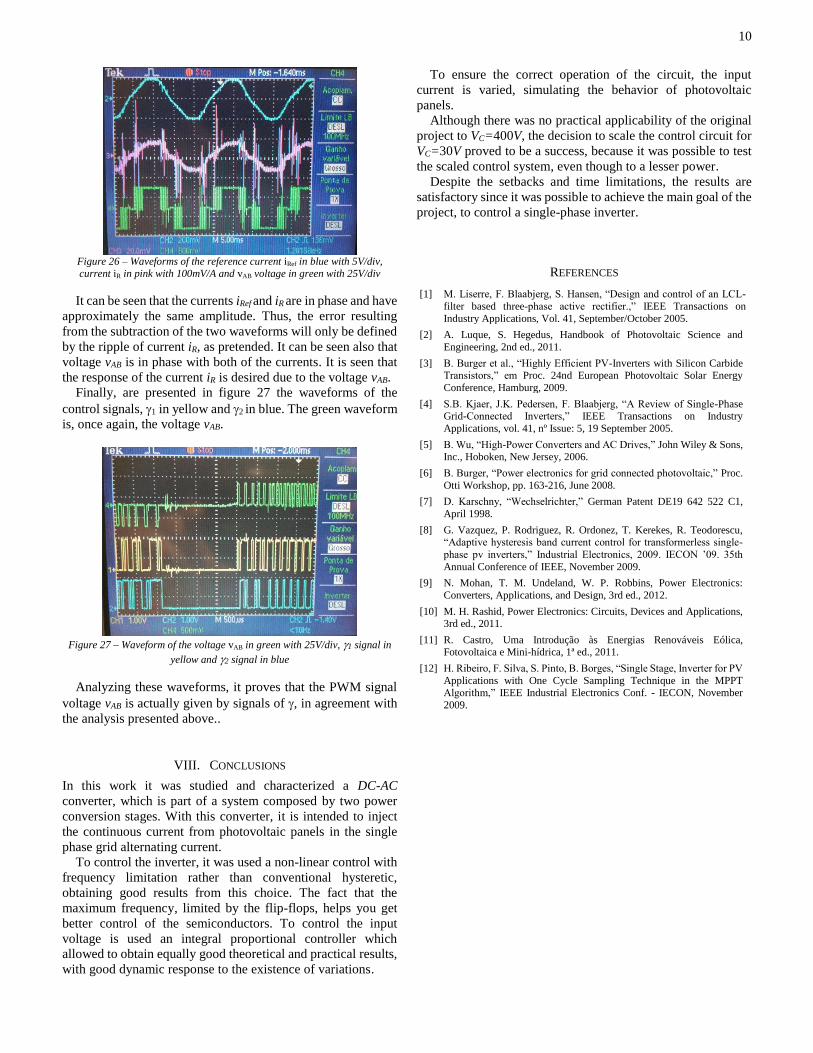
Figure 26 – Waveforms of the reference current iRef in blue with 5V/div, current iR in pink with 100mV/A and vAB voltage in green with 25V/div
It can be seen that the currents iRef and iR are in phase and have
approximately the same amplitude. Thus, the error resulting
from the subtraction of the two waveforms will only be defined
by the ripple of current iR, as pretended. It can be seen also that
voltage vAB is in phase with both of the currents. It is seen that
the response of the current iR is desired due to the voltage vAB.
Finally, are presented in figure 27 the waveforms of the
control signals, 1 in yellow and 2 in blue. The green waveform
is, once again, the voltage vAB.
Figure 27 – Waveform of the voltage vAB in green with 25V/div, 1 signal in
yellow and 2 signal in blue
Analyzing these waveforms, it proves that the PWM signal
voltage vAB is actually given by signals of , in agreement with
the analysis presented above..
VIII. CONCLUSIONS
In this work it was studied and characterized a DC-AC
converter, which is part of a system composed by two power
conversion stages. With this converter, it is intended to inject
the continuous current from photovoltaic panels in the single
phase grid alternating current.
To control the inverter, it was used a non-linear control with
frequency limitation rather than conventional hysteretic,
obtaining good results from this choice. The fact that the
maximum frequency, limited by the flip-flops, helps you get
better control of the semiconductors. To control the input
voltage is used an integral proportional controller which
allowed to obtain equally good theoretical and practical results,
with good dynamic response to the existence of variations.
To ensure the correct operation of the circuit, the input
current is varied, simulating the behavior of photovoltaic
panels.
Although there was no practical applicability of the original
project to VC=400V, the decision to scale the control circuit for
VC=30V proved to be a success, because it was possible to test
the scaled control system, even though to a lesser power.
Despite the setbacks and time limitations, the results are
satisfactory since it was possible to achieve the main goal of the
project, to control a single-phase inverter.
REFERENCES
[1] M. Liserre, F. Blaabjerg, S. Hansen, “Design and control of an LCL-
filter based three-phase active rectifier.,” IEEE Transactions on
Industry Applications, Vol. 41, September/October 2005.
[2] A. Luque, S. Hegedus, Handbook of Photovoltaic Science and
Engineering, 2nd ed., 2011.
[3] B. Burger et al., “Highly Efficient PV-Inverters with Silicon Carbide Transistors,” em Proc. 24nd European Photovoltaic Solar Energy
Conference, Hamburg, 2009.
[4] S.B. Kjaer, J.K. Pedersen, F. Blaabjerg, “A Review of Single-Phase Grid-Connected Inverters,” IEEE Transactions on Industry
Applications, vol. 41, nº Issue: 5, 19 September 2005.
[5] B. Wu, “High-Power Converters and AC Drives,” John Wiley & Sons, Inc., Hoboken, New Jersey, 2006.
[6] B. Burger, “Power electronics for grid connected photovoltaic,” Proc.
Otti Workshop, pp. 163-216, June 2008.
[7] D. Karschny, “Wechselrichter,” German Patent DE19 642 522 C1,
April 1998.
[8] G. Vazquez, P. Rodriguez, R. Ordonez, T. Kerekes, R. Teodorescu, “Adaptive hysteresis band current control for transformerless single-
phase pv inverters,” Industrial Electronics, 2009. IECON ’09. 35th
Annual Conference of IEEE, November 2009.
[9] N. Mohan, T. M. Undeland, W. P. Robbins, Power Electronics:
Converters, Applications, and Design, 3rd ed., 2012.
[10] M. H. Rashid, Power Electronics: Circuits, Devices and Applications, 3rd ed., 2011.
[11] R. Castro, Uma Introdução às Energias Renováveis Eólica, Fotovoltaica e Mini-hídrica, 1ª ed., 2011.
[12] H. Ribeiro, F. Silva, S. Pinto, B. Borges, “Single Stage, Inverter for PV
Applications with One Cycle Sampling Technique in the MPPT Algorithm,” IEEE Industrial Electronics Conf. - IECON, November
2009.