Embed Size (px)
Citation preview

RT5047A
Copyright © 2016 Richtek Technology Corporation. All rights reserved. is a registered trademark of Richtek Technology Corporation.
DS5047A-01 November 2016 www.richtek.com 1
Single Output LNB Supply and Control Voltage Regulator
General Description
The RT5047A is a highly integrated voltage regulator
and interface IC, specifically design for supplying
power and control signals from advanced satellite
set-top box (STB) modules to the LNB down-converter
in the antenna dish or to the multi-switch box.
The device is consists of the independent current-mode
boost controller and low dropout linear regulator along
with the circuitry required for 22KHz tone shaping to
support DiSEqCTM1.x communications.
The RT5047A has fault protection (over-current,
over-temperature and under-voltage lockout).
The RT5047A are available in a SOP-8 (Exposed Pad)
package to achieve optimized solution for thermal
dissipation.
Ordering Information
RT5047A
Package Type
SP : SOP-8 (Exposed Pad-Option 2)
Lead Plating System
G : Green (Halogen Free and Pb Free)
Note :
Richtek products are :
RoHS compliant and compatible with the current
requirements of IPC/JEDEC J-STD-020.
Suitable for use in SnPb or Pb-free soldering
processes.
Features Wide Input Supply Voltage Range : 8V to 16V
Output Current Limit of 550mA with 45ms timer
Low Noise LNB Output Voltage (13.3V and 18.3V
by SEL Pin)
3% High Accuracy for 0mA to 500mA Current
Output
Push-Pull Output Stage minimizes 13.3V to
18.3V and 18.3V to 13.3V Output Transition Time
External 22kHz Tone Input
Meet DiSEqCTM1.x Protocol
Output Short Circuit Protection
Over-Temperature Protection
Applications LNB Power Supply and Control for Satellite Set-Top
Box
Analog and Digital Satellite Receivers/Satellite TV,
Satellite PC cards
Pin Configurations
(TOP VIEW)
LNB
BOOST
LX
VIN
TONE
FAULT
EN
SELGND
2
3
4 5
6
7
8
9
SOP-8 (Exposed Pad)
Simplified Application Circuit
VIN
CBST
VIN
RT5047A
L1
LX
SEL
TONE
GND
LNB
CLNB
Max. 550mA
CIN2
CIN1
BOOST
EN
VLNB
D1
D2 D4
D3
D5

RT5047A
Copyright © 2016 Richtek Technology Corporation. All rights reserved. is a registered trademark of Richtek Technology Corporation.
www.richtek.com DS5047A-01 November 2016 2
Marking Informaton
RT5047A
GSPYMDNN
RT5047AGSP : Product Number
YMDNN : Date Code
Functional Pin Description Pin No. Pin Name Pin Function
1 LNB Output voltage for LNB.
2 BOOST Boost output and tracking supply voltage to LNB.
3 LX Switching node of DC-DC boost converter.
4 VIN Power supply input.
5 EN LNB output enable.
6 SEL LNB output voltage selection pin (Low is for 13.3V, high is for 18.3V).
7 FAULT Fault detection pin. Pull to 3.3V by 4.7k resistor.
8 TONE 22kHz TONE input.
9 (Exposed Pad) GND Ground. The exposed pad must be soldered to a large PCB and connected
to GND for maximum power dissipation.
Function Block Diagram
Oscillator
2-steps
Voltage
Setting
GND
VIN
Reference
Voltage
VR1
Bandgap
Reference
VD2Dynamic
Dropout
Control
BOOST
OSC
VUD
VFB1
VR1
PWM
Controller
DA
C
VD1
LX
Error
Amp
RF1 RF2
LNBLinear
Regulator
OCP2
Logic
OCP1
UVLO
OTP
SEL
EN
FAULT
22kHz Tone ShapeTONE VFB2

RT5047A
Copyright © 2016 Richtek Technology Corporation. All rights reserved. is a registered trademark of Richtek Technology Corporation.
DS5047A-01 November 2016 www.richtek.com 3
Operation
The RT5047A integrates a current mode boost
converter and linear regulator. Use the SEL pin to
control the LNB voltage and the boost converter track is
at least greater 850mV than LNB voltage. The boost
converter is the high efficiency PWM architecture with
700kHz operation frequency. The linear regulator has
the capability to source current up to 550mA during
continuous operation. All the loop compensation,
current sensing, and slope compensation functions are
provided internally.
OCP
Both the boost converter and the linear regulator have
independent current limit. In the boost converter
(OCP1), this is achieved through cycle-by-cycle
internal current limit (typ. 3A). In the linear regulator
(OCP2), when the linear regulator exceeds OCP more
than 48ms, the LNB output will be disabled and re-start
after 1.8s.
Tone Circuit
This circuit is used for tone generation. Use the TONE
pin to control output amplitude of LNB.
OTP
When the junction temperature reaches the critical
temperature (typically 150C), the boost converter and
the linear regulator are immediately disabled.
UVLO
The UVLO circuit compares the VIN with the UVLO
threshold (7.7V rising typically) to ensure that the input
voltage is high enough for reliable operation. The
350mV (typ.) hysteresis prevents supply transients
from causing a shutdown.
PWM Controller
The loop compensation, current sensing, and slope
compensation functions are provided internally.

RT5047A
Copyright © 2016 Richtek Technology Corporation. All rights reserved. is a registered trademark of Richtek Technology Corporation.
www.richtek.com DS5047A-01 November 2016 4
Absolute Maximum Ratings (Note 1)
Supply Input Voltage, VIN ------------------------------------------------------------------------------------------- 0.3V to 28V
Output Voltage LNB, LX and BOOST Pins --------------------------------------------------------------------- 0.3V to 30V
Others Pin to GND ---------------------------------------------------------------------------------------------------- 0.3V to 6V
Power Dissipation, PD @ TA = 25C
SOP-8 (Exposed pad) ------------------------------------------------------------------------------------------------ 3.44W
Package Thermal Resistance (Note 2)
SOP-8 (Exposed pad), JA ------------------------------------------------------------------------------------------ 29C/W
SOP-8 (Exposed pad), JC ------------------------------------------------------------------------------------------ 2C/W
Lead Temperature (Soldering, 10 sec.) -------------------------------------------------------------------------- 260C
Junction Temperature ------------------------------------------------------------------------------------------------ 150C
Storage Temperature Range --------------------------------------------------------------------------------------- 65C to 150C
ESD Susceptibility (Note 3)
HBM (Human Body Model)----------------------------------------------------------------------------------- 2kV
Recommended Operating Conditions (Note 4)
Supply Input Voltage ------------------------------------------------------------------------------------------------- 8V to 16V
Ambient Temperature Range--------------------------------------------------------------------------------------- 40C to 85C
Junction Temperature Range -------------------------------------------------------------------------------------- 40C to 125C
Electrical Characteristics (VIN (typ.) = 12V, VIN = 8V to 16V, TA = 25C, unless otherwise specified)
Parameter Symbol Test Conditions Min Typ Max Unit
General
LNB Output Accuracy,
Load and Line Regulation ERR
Relative to selected VLNB target level,
ILNB = 0 to 450mA 3 -- 3 %
Supply Current
IIN_OFF EN = 0, LNB output disabled -- 0.3 0.5 mA
IIN_ON EN = 1, VLNB = 18.3V, Tone = 0V -- 10 18 mA
IIN_ON EN = 1, VLNB = 18.3V, 22kHz TONE
Input -- 16 28 mA
Boost Switch On
Resistance RDS(ON) ILNB = 450mA -- 150 300 m
Switching Frequency fSW 600 700 800 kHz
Switch Current Limit ILIMSW VIN = 10V, VLNB = 20.5V -- 3 -- A
Linear Regulator Voltage
Drop VDROP VBOOST-VLNB, ILNB = 450mA -- 0.85 -- V
Output Voltage Rise Time TR_LNB For VLNB = 13.3V18.3V,
CLNB = 100nF, ILNB = 450mA -- 3 10 ms
Output Voltage Pull-Down
Time TF_LNB
For VLNB = 18.3V13.3V,
CLNB = 100nF, ILNB = 0mA -- 3 10 ms

RT5047A
Copyright © 2016 Richtek Technology Corporation. All rights reserved. is a registered trademark of Richtek Technology Corporation.
DS5047A-01 November 2016 www.richtek.com 5
Parameter Symbol Test Conditions Min Typ Max Unit
Ripple and Noise on LNB
Output VRIP_PP 20MHz bandwidth limit (GBD) -- 20 -- mVPP
Load Regulation VOUT_LOAD VLNB = 13.3V, ILNB = 50mA to 450mA -- 38 76
mV VLNB = 18.3V, ILNB = 50mA to 450mA -- 45 90
Line Regulation VOUT_LINE
VIN = 9 to 14V, VLNB = 13.3V,
ILNB = 50mA 10 -- 10
mV VIN = 9 to 14V, VLNB = 18.3V,
ILNB = 50mA 10 -- 10
Protection
Output Over-Current Limit ILIM_LNB1 VLNB = 13.3V/18.3V 500 550 650 mA
Output Over-Current
Disable Time TDIS_ON VLNB short to GND -- 45 -- ms
Output Over-Current
Disable Time TDIS_OFF VLNB short to GND (GBD) -- 1800 -- ms
VIN Under-Voltage Lockout
Threshold VUVLO VIN Fflling -- 7.35 -- V
VIN Turn On Threshold VIN_TH VIN rising -- 7.7 8 V
VIN Under-Voltage Lockout
Hysteresis VUVLOHYS -- 350 -- mV
OTP Threshold TOTP -- 140 -- oC
OTP Hysteresis TOTPHYS -- 15 -- oC
TONE
TONE Frequency FTONE 20 22 24 kHz
TONE Amplitude, Peak to
Peak VTONE_PP ILNB = 50 to 450mA, CLNB = 200nF 550 700 900 mVPP
TONE Duty Cycle DCTONE ILNB = 0 to 450mA, CLNB = 570nF 40 50 60 %
TONE Rise Time TRTONE ILNB = 0 to 450mA, CLNB = 570nF 5 10 15 s
TONE Fall Time TFTONE ILNB = 0 to 450mA, CLNB = 570nF 5 10 15 s
TONE Logic Input VTONE_H 1.2 -- -- V
VTONE_L -- -- 0.4 V
TONE Input Leakage ITONELKG -- 5 10 A
ENABLE, SEL Pins
EN Logic Input VEN_H 1.2 -- -- V
VEN_L -- -- 0.4 V
EN Input Leakage IENLKG -- 5 10 A
SEL Logic Input VSEL_H 1.2 -- -- V
VSEL_L -- -- 0.4 V
SEL Input Leakage ISELLKG -- 5 10 A

RT5047A
Copyright © 2016 Richtek Technology Corporation. All rights reserved. is a registered trademark of Richtek Technology Corporation.
www.richtek.com DS5047A-01 November 2016 6
Note 1. Stresses beyond those listed “Absolute Maximum Ratings” may cause permanent damage to the device. These are
stress ratings only, and functional operation of the device at these or any other conditions beyond those indicated in the
operational sections of the specifications is not implied. Exposure to absolute maximum rating conditions may affect
device reliability.
Note 2. JA is measured at TA = 25C on a high effective thermal conductivity four-layer test board per JEDEC 51-7. JC is
measured at the exposed pad of the package.
Note 3. Devices are ESD sensitive. Handling precaution is recommended.
Note 4. The device is not guaranteed to function outside its operating conditions.
Note 5. Operation at VIN = 16V may be limited by power loss in the linear regulator.

RT5047A
Copyright © 2016 Richtek Technology Corporation. All rights reserved. is a registered trademark of Richtek Technology Corporation.
DS5047A-01 November 2016 www.richtek.com 7
Typical Application Circuit
VINCBST
20μF/30μF
VIN
RT5047A
L1
10μF
LX
SEL
TONE
GND
LNB
CLNB
0.1μF
Max. 550mA
CIN2
1μF
CIN1
2x10μF
BOOST
EN
VLNB
D1
SS14
D2
SS14
D4
SMDJ20A
D3
SS14
D5
SS141
23
4
5
8
6
9 (Exposed Pad)
Note :
1. D2, D3, D4, D5 are used for surge protection.
2. The capacitor C3 should not be less than 1F for the power stability.
3. EN, TONE and SEL are connected to microcontroller directly.

RT5047A
Copyright © 2016 Richtek Technology Corporation. All rights reserved. is a registered trademark of Richtek Technology Corporation.
www.richtek.com DS5047A-01 November 2016 8
Typical Operating Characteristics
Boost Efficiency vs. Output Current
60
65
70
75
80
85
90
95
100
0.00 0.10 0.20 0.30 0.40 0.50 0.60
Output Current (A)
Effic
ien
cy (
%)
VIN = 12V, VBOOST = 14.3V
System Efficiency vs. Output Current
60
65
70
75
80
85
90
95
100
0.00 0.10 0.20 0.30 0.40 0.50 0.60
Output Current (A)
Effic
ien
cy (
%)
VIN = 12V, VBOOST = 14.3V, VLNB = 13.3V
Tone Amplitude vs. Temperature
0.55
0.60
0.65
0.70
0.75
0.80
0.85
0.90
-50 -25 0 25 50 75 100 125
Temperature (°C)
To
ne
Am
plit
ud
e (
V)
VIN = 12V, VLNB = 13.3V, TONE enable
Tone Amplitude vs. Output Current
0.55
0.60
0.65
0.70
0.75
0.80
0.85
0.90
0 0.1 0.2 0.3 0.4 0.5 0.6
Output Current (A)
To
ne
Am
plit
ud
e (
V)
VIN = 12V, VLNB = 13.3V, TONE enable
Output Voltage vs. Temperature
12
13
14
15
16
17
18
19
-50 -25 0 25 50 75 100 125
Temperature (°C)
Ou
tpu
t V
olta
ge
(V
)
VIN = 12V
VLNB_18.3V
VLNB_13.3V
Output Voltage vs. Output Current
12
13
14
15
16
17
18
19
0.00 0.10 0.20 0.30 0.40 0.50 0.60
Output Current (A)
Ou
tpu
t V
olta
ge
(V
)
VLNB_13.3V
VIN = 12V
VLNB_ 18.3V

RT5047A
Copyright © 2016 Richtek Technology Corporation. All rights reserved. is a registered trademark of Richtek Technology Corporation.
DS5047A-01 November 2016 www.richtek.com 9
Over Current Protect vs. Temperature
0.50
0.55
0.60
0.65
0.70
-25 0 25 50 75 100 125
Temperature (°C)
Cu
rre
nt (A
)
VIN = 12V, VLNB = 13.3V
Under Voltage Lockout vs. Temperature
7.00
7.20
7.40
7.60
7.80
8.00
-50 -25 0 25 50 75 100 125
Temperature (°C)
Un
de
r V
olta
ge
Lo
cko
ut (V
) 1
VIN = 12V
VLNB_ac
(200mV/Div)
Time (50s/Div)
Tone Output
VIN = 12V VSEL from 0V to 3.3V,
CLNB = 0.1F, VLNB from 13V to 18V
VLNB
(5V/Div)
VSEL
(2V/Div)
Time (500s/Div)
Output Voltage Transition Rising
VIN = 12V, VSEL from 3.3V to 0V,
CLNB = 1F, VLNB from 18V to 13V
VLNB
(5V/Div)
VSEL
(2V/Div)
Time (500s/Div)
Output Voltage Transition Falling
VIN = 12V
VIN
(10V/Div)
VBOOST
(10V/Div)
VLNB
(10V/Div)
Time (5ms/Div)
Power On Sequence
RT5047A
Copyright © 2016 Richtek Technology Corporation. All rights reserved. is a registered trademark of Richtek Technology Corporation.
www.richtek.com DS5047A-01 November 2016 10
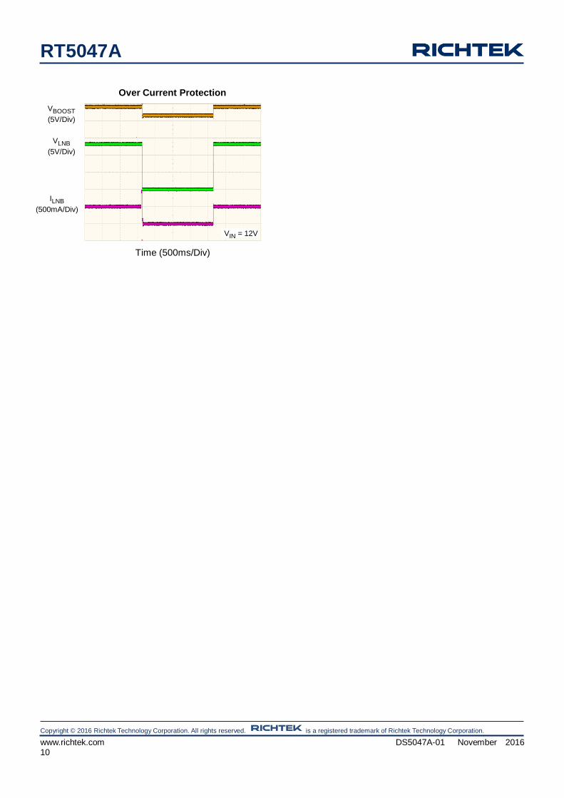
VIN = 12V
VBOOST
(5V/Div)
VLNB
(5V/Div)
ILNB
(500mA/Div)
Time (500ms/Div)
Over Current Protection

RT5047A
Copyright © 2016 Richtek Technology Corporation. All rights reserved. is a registered trademark of Richtek Technology Corporation.
DS5047A-01 November 2016 www.richtek.com 11
Application Information
Boost Converter/Linear Regulator
The 5047A integrates a current-mode boost converter
and linear regulator. Use the SEL pin to control the
LNB voltage and the boost converter track is at least
greater 800mV than the LNB voltage. The boost
converter is high efficiency PWM architecture with
700kHz operation frequency. The linear regulator has
the capability to source current up to 550mA during
continuous operation. All the loop compensation,
current sensing, and slope compensation functions are
provided internally.
The RT5047A has current limiting on the boost
converter and the LNB output to protect the IC against
short circuits. The internal MOSFET will turn off when
the LX current is higher than 3A cycle-by-cycle. The
LNB output will turn off when the output current higher
than the 550mA and 45ms and turn-on after 1800ms
automatically.
Input Capacitor Selection
The input capacitor reduces voltage spikes from the
input supply and minimizes noise injection to the
converter. A 30F capacitance is sufficient for most
applications. Nevertheless, a higher or lower value may
be used depending on the noise level from the input
supply and the input current to the converter. Note that
the voltage rating of the input capacitor must be greater
than the maximum input voltage.
Inductor Selection
The inductance depends on the maximum input current.
As a general rule, the inductor ripple current range is
20% to 40% of the maximum input current. If 40% is
selected as an example, the inductor ripple current can
be calculated according to the following equations :
OUT OUT(MAX)IN(MAX)
IN
RIPPLE IN(MAX)
V II =
V
I = 0.4 I
where η is the efficiency of the converter, IIN(MAX) is
the maximum input current, and IRIPPLE is the
inductor ripple current. The input peak current can
then be obtained by adding the maximum input current
with half of the inductor ripple current as shown in the
following equation :
IPEAK = 1.2 x IIN(MAX)
note that the saturated current of the inductor must be
greater than IPEAK. The inductance can eventually be
determined according to the following equation :
2
2
IN OUT IN
OUT OUT(MAX) OSC
η V V VL
0.4 V I f
where fOSC is the switching frequency. For better
system performance, a shielded inductor is preferred to
avoid EMI problems.
Boost Output Capacitor Selection
The RT5047A boost regulator is internally
compensated and relies on the inductor and output
capacitor value for overall loop stability. The output
capacitor is in the 30F to 50F range with a low ESR,
as strongly recommended. The voltage rating on this
capacitor should be in the 25V to 35V range since it is
connected to the boost VOUT rail.
The output ripple voltage is an important index for
estimating chip performance. This portion consists of
two parts. One is the product of the inductor current
with the ESR of the output capacitor, while the other
part is formed by the charging and discharging process
of the output capacitor. As shown in Figure 1, VOUT1
can be evaluated based on the ideal energy
equalization. According to the definition of Q, the Q
value can be calculated as the following equation :
IN L OUT IN L OUT
INOUT OUT1
OUT OSC
1 1 1Q = I I I I I I
2 2 2
V 1 = C V
V f
where fOSC is the switching frequency and IL is the
inductor ripple current. Bring COUT to the left side to
estimate the value of VOUT1 according to the following
equation :
OUTOUT1
OUT OSC
D IV =
C f

RT5047A
Copyright © 2016 Richtek Technology Corporation. All rights reserved. is a registered trademark of Richtek Technology Corporation.
www.richtek.com DS5047A-01 November 2016 12
where D is the duty cycle and η is the boost converter
efficiency. Finally, take ESR into consideration, the
overall output ripple voltage can be determined by the
following equation :
OUTOUT IN
OUT OSC
D IV = I ESR
C f
The output capacitor, COUT, should be selected
accordingly.
Time
Time
Inductor Current
Output Current
Output Ripple
Voltage (ac)
(1-D)TS
ΔVOUT1
ΔIL
Input Current
Figure 1. The Output Ripple Voltage without the
Contribution of ESR
Schottky Diode Selection
Schottky diodes are chosen for their low
forward-voltage drop and fast switching speed.
However, when making a selection, important
parameters such as power dissipation, reverse voltage
rating, and pulsating peak current should all be taken
into consideration. A suitable Schottky diode’s reverse
voltage rating must be greater than the maximum
output voltage and its average current rating must
exceed the average output current. The chosen diode
should also have a sufficiently low leakage current level,
since it increases with temperature.
Under-Voltage Lockout (UVLO)
The UVLO circuit compares the input voltage at VIN
with the UVLO threshold (7.7V rising typically) to
ensure that the input voltage is high enough for reliable
operation. The 350mV (typ.) hysteresis prevents supply
transients from causing a shutdown. Once the input
voltage exceeds the UVLO rising threshold, start-up
begins. When the input voltage falls below the UVLO
falling threshold, all IC internal functions will be turned
off by the controller.
Over-Current Protection
The RT5047A features an over-current protection
function to prevent chip damage from high peak
currents. Both the boost converter and the linear
regulator have independent current limit. In the boost
converter, this is achieved through cycle-by-cycle
internal current limit. During the ON-period, the chip
senses the inductor current that is flowing into the LX
pin. The internal NMOS will be turned off if the peak
inductor current reaches the current-limit value of 3A
(typ.).When the linear regulator exceeds 550mA (typ.)
more than 45ms, the LNB output will be disabled.
During this period of time, if the current limit condition
disappears, the OCP will be cleared and the part
restarts. If the part is still in current limit after this time
period, the linear regulator and boost converter will
automatically disable to prevent the part from
overheating.
Short Circuit Protection
If the LNB output is shorted to ground, and more than
45ms, the RT5047A will be disabled 1.8s then enable
automatically.
Over-Temperature Protection
When the junction temperature reaches the critical
temperature (typically 140 oC), the boost converter and
the linear regulator are immediately disabled. When the
junction temperature cools down to a lower
temperature threshold specified, the RT5047A will be
allowed to restart by normal start operation.
LNB Output Voltage
The RT5047A has voltage control function on the LNB
output. This function provides 4 levels for the common
standards and compensation if the cable line has
voltage drop. These voltage levels are defined in table
1. The rise time and fall time of the VLNB is 3mS (typ.).

RT5047A
Copyright © 2016 Richtek Technology Corporation. All rights reserved. is a registered trademark of Richtek Technology Corporation.
DS5047A-01 November 2016 www.richtek.com 13
Table 1
SEL Pin Status LNB Output Voltage
0 13.3V
1 18.3V
Tone Generation
The RT5047A provides the tone generation function, please refer to the Figure 2. Set the TONE pin with 22kHz logic
signal, the LNB linear regulator output will carry a 22kHz, 700mV peak to peak signal for DiSEqC 1.x communication.
It can meet base-band timings of 500s (±100s) for a one-third bit PWK coded signal period on a nominal 22kHz
(±20 %).
TONE
signal0V
3.3V
13.3V or
18.3V700m
V
LNB
TONE signal
detect time
VLNB close
TONE after
TONE signal
detect time
VLNB output
TONE when
TONE signal
rise up
Figure 2. Tone Generation Options
Pull-Down Rate Control
The output linear stage provides approximately 40mA
of pull-down capability. This ensures that the output
volts are ramped from 18.3V to 13.3V in a reasonable
amount of time.
Over-Current Disable Time
If the LNB output current exceeds 550mA, typical, for
more than 45ms, then the LNB output will be disabled
and device enters a TON = 45ms/TOFF = 1800ms
routine. It will be returned to normal operation after a
successful soft-start process.
Inrush Current
At start-up or during a LNB reconfiguration event, a
transient surge current above the normal DC operating
level can be provided by the IC. This current increase
can be as high as 550mA, typical, for as long as
required, up to a maximum of 45ms.
OCP1=1000mA
25msOCP2=550mA
20ms
If loading is 1000mA
1800ms
OCP1=1000mA
25msOCP2=550mA
20ms
OCP1=250mA
25msOCP2=138mA
20ms
If LNB is shorted to GND
1800ms
OCP1=250mA
25msOCP2=138mA
20ms

RT5047A
Copyright © 2016 Richtek Technology Corporation. All rights reserved. is a registered trademark of Richtek Technology Corporation.
www.richtek.com DS5047A-01 November 2016 14
DC Current
The RT5047A can handle up to 500mA during
continuous operation.
Thermal Considerations
For continuous operation, do not exceed absolute
maximum junction temperature. The maximum power
dissipation depends on the thermal resistance of the IC
package, PCB layout, rate of surrounding airflow, and
difference between junction and ambient temperature.
The maximum power dissipation can be calculated by
the following formula :
PD(MAX) = (TJ(MAX) TA) / JA
where TJ(MAX) is the maximum junction temperature,
TA is the ambient temperature, and JA is the junction to
ambient thermal resistance.
For recommended operating condition specifications,
the maximum junction temperature is 125C. The
junction to ambient thermal resistance, JA, is layout
dependent. For SOP-8 (Exposed Pad) package, the
thermal resistance, JA, is 29C/W on a standard
JEDEC 51-7 four-layer thermal test board. The
maximum power dissipation at TA = 25C can be
calculated by the following formula :
PD(MAX) = (125C 25C) / (29C/W) = 3.44W for
SOP-8 (Exposed Pad) package
The maximum power dissipation depends on the
operating ambient temperature for fixed TJ(MAX) and
thermal resistance, JA. The derating curve in Figure 3
allows the designer to see the effect of rising ambient
temperature on the maximum power dissipation.
Figure 3. Derating Curve of Maximum Power
Dissipation
0.0
0.5
1.0
1.5
2.0
2.5
3.0
3.5
4.0
4.5
5.0
0 25 50 75 100 125
Ambient Temperature (°C)
Ma
xim
um
Po
we
r D
issip
atio
n (
W) 1 Four-Layer PCB

RT5047A
Copyright © 2016 Richtek Technology Corporation. All rights reserved. is a registered trademark of Richtek Technology Corporation.
DS5047A-01 November 2016 www.richtek.com 15
Layout Consideration
For high frequency switching power supplies, the PCB layout is important to get good regulation, high efficiency and
stability. The following descriptions are the guidelines for better PCB layout.
For good regulation, place the power components as close as possible. The traces should be wide and short
enough especially for the high-current loop.
Minimize the size of the LX node and keep it wide and shorter.
The exposed pad of the chip should be connected to a strong ground plane for maximum thermal consideration.
LNB
BOOST
LX
VIN
TONE
FAULT
SEL
EN
GND
VIN
L1
VOUT
D3 and D4 should be placed
as closed as possible to
VOUT for surge protection.
The inductor should be placed as close as possible to the LX pin to minimize the
noise coupling into other circuits.
LX node copper area should be minimized for reducing EMI
Place the power components as close as possible. The traces should be wide and
short especially for the high-current loop.
The CIN, CBST and CLNB
should be placed as closed
as possible to RT5047 for
good filter.
CIN1 CIN2
D1
D2
D3
D4
CBST1 CBST3CBST2
CLNB1
The exposed pad of the chip
s h o u l d b e c o n n e c t e d t o
ana log g round p lane fo r
thermal consideration.
The TONE, SEL and EN pin
should be connected to MCU
or GND. Do not floating these
pins.
Figure 4. PCB Layout Guide

RT5047A
Copyright © 2016 Richtek Technology Corporation. All rights reserved. is a registered trademark of Richtek Technology Corporation.
www.richtek.com DS5047A-01 November 2016 16
Outline Dimension
Symbol Dimensions In Millimeters Dimensions In Inches
Min Max Min Max
A 4.801 5.004 0.189 0.197
B 3.810 4.000 0.150 0.157
C 1.346 1.753 0.053 0.069
D 0.330 0.510 0.013 0.020
F 1.194 1.346 0.047 0.053
H 0.170 0.254 0.007 0.010
I 0.000 0.152 0.000 0.006
J 5.791 6.200 0.228 0.244
M 0.406 1.270 0.016 0.050
Option 1 X 2.000 2.300 0.079 0.091
Y 2.000 2.300 0.079 0.091
Option 2 X 2.100 2.500 0.083 0.098
Y 3.000 3.500 0.118 0.138
8-Lead SOP (Exposed Pad) Plastic Package
Richtek Technology Corporation
14F, No. 8, Tai Yuen 1st Street, Chupei City
Hsinchu, Taiwan, R.O.C.
Tel: (8863)5526789 Richtek products are sold by description only. Richtek reserves the right to change the circuitry and/or specifications without notice at any time. Customers should obtain the latest relevant information and data sheets before placing orders and should verify that such information is current and complete. Richtek cannot assume responsibility for use of any circuitry other than circuitry entirely embodied in a Richtek product. Information furnished by Richtek is believed to be accurate and reliable. However, no responsibility is assumed by Richtek or its subsidiaries for its use; nor for any infringements of patents or other rights of third parties which may result from its use. No license is granted by implication or otherwise under any patent or patent rights of Richtek or its subsidiaries.