Embed Size (px)
Citation preview

IEEE JOURNAL OF SOLID-STATE CIRCUITS, VOL. 38, NO. 1, JANUARY 2003 89
Single-Inductor Multiple-Output SwitchingConverters With Time-Multiplexing Control
in Discontinuous Conduction ModeDongsheng Ma, Student Member, IEEE, Wing-Hung Ki, Member, IEEE, Chi-Ying Tsui, Member, IEEE, and
Philip K. T. Mok, Senior Member, IEEE
Abstract—An integrated single-inductor dual-output boost con-verter is presented. This converter adopts time-multiplexing con-trol in providing two independent supply voltages (3.0 and 3.6 V)using only one 1- H off-chip inductor and a single control loop.This converter is analyzed and compared with existing counter-parts in the aspects of integration, architecture, control scheme,and system stability. Implementation of the power stage, the con-troller, and the peripheral functional blocks is discussed. The de-sign was fabricated with a standard 0.5- m CMOS n-well process.At an oscillator frequency of 1 MHz, the power conversion effi-ciency reaches 88.4% at a total output power of 350 mW. Thistopology can be extended to have multiple outputs and can be ap-plied to buck, flyback, and other kinds of converters.
Index Terms—Cross regulation, discontinuous conductionmode (DCM), pulsewidth modulation (PWM), single-inductordual-output (SIDO) converter, single-inductor multiple-output(SIMO) converter, time-multiplexing (TM) control.
I. INTRODUCTION
W ITH THE proliferation of battery-operated portable ap-plications such as personal digital assistants and mobile
phones, minimizing power consumption becomes one of themost important design criteria. It has been shown that voltagescaling and effective power management are the most effectiveways in reducing the power consumption for digital systems[1]. Recent works showed that having multiple supply voltagescan further reduce the power consumption at different designabstraction levels [2]–[7]. In [3], an energy-efficient high-levelscheduling and allocation algorithm exploiting multiple supplyvoltages was proposed. In [4], system-level memory power op-timization technique using multiple supply voltages was dis-cussed. Gate- and system-level power reduction techniques uti-lizing multiple supply voltages were presented in [5], [6], and[7]. In these works, it is assumed that multiple supply voltagesare available on-chip. Yet, details of the supply voltage gener-ation were not discussed. Traditional on-chip dc–dc convertersonly provide one supply voltage for the core of the chip [8].These designs cannot be directly adapted to systems that require
Manuscript received March 12, 2002; revised August 6, 2002. This work wassupported in part by the Hong Kong Research Grant Council under Grant CERGHKUST 6209/01E.
The authors are with the Department of Electrical and Electronic Engineering,The Hong Kong University of Science and Technology, Hong Kong, China(e-mail: [email protected]).
Digital Object Identifier 10.1109/JSSC.2002.806279
(a)
(b)
Fig. 1. Isolated multiple-output converters. (a) Forward converter. (b) Flybackconverter.
multiple supply voltages. To reduce the number of power andground pins and to have a clean power supply, an on-chip dc–dcconverter that can provide multiple output voltages is desirablefor these applications. In this paper, we address the issues ofdesigning an on-chip single-inductor multiple-output (SIMO)dc–dc converter.
Conventional implementation of a dc–dc converter that hasoutput voltages may consist of independent converters,
or employ a transformer that has secondary windingsto distribute energy into the various outputs (isolated mul-tiple-output converter) [Fig. 1(a) and 1(b)] [9], [10]. The firstmethod requires too many components, including controllersand power devices, and this will increase the system cost.The second method does not allow individual outputs to be
0018-9200/03$17.00 © 2003 IEEE

90 IEEE JOURNAL OF SOLID-STATE CIRCUITS, VOL. 38, NO. 1, JANUARY 2003
Fig. 2. Two boost converters with interleaving inductor currents in DCM.
precisely controlled and has a big limitation for the applica-tions of multiple voltage supply scaling. In addition, leakageinductance and cross coupling among windings cause a seriouscross-regulation problem. Moreover, both methods require atleast inductors or windings, which may be too bulky andcostly. In [11], a multiple-output architecture was proposedwhich combines the control loops of converters into a singleone. Multiple inductors are still needed and the reduction inexternal components is very small.
In this paper, we introduce a new single-inductor dual-output(SIDO) dc–dc converter [12]. Only a single inductor is requiredfor providing two different output voltages. Using a novel time-multiplexing (TM) control scheme, the converter only needs onecontroller to regulate all the outputs. Compared with other de-signs, both on-chip and off-chip components are reduced sig-nificantly. Implementation issues such as synchronous rectifica-tion, controller design, current detection, dead-time buffer, andringing suppression techniques are also addressed. The designof a SIDO boost converter has been fabricated using a standard0.5- m CMOS n-well process. Experimental results verify thevalidity of the design. The topology can easily be extended togive multiple outputs and to implement buck and flyback con-verter architectures. The remainder of the paper is organized asfollows. Section II describes the basic architecture and controlstrategy of the proposed converter. Section III discusses the im-plementation details of the design. Section IV presents experi-mental results and Section V concludes our research efforts.
II. SIMO BOOSTCONVERTER
A. Architecture and Control Strategy
Consider two conventional boost converters A and B workingat the same switching frequency. If both converters are workingin the discontinuous conduction mode (DCM), a possiblescheme of their inductor currents could be as shown in Fig. 2.For Converter A, during , the inductor current rampsup and the inductor is charged with a voltage of ,where is the duty ratio, is the switching period andis the voltage of the source. During , ramps downwith , and during , stays zero.A similar scheme also applies to Converter B. Obviously, if
and , the two inductorcurrents can be alternately assigned to occupy different partsof the switching cycle without affecting each other. Hence, aSIDO converter can be obtained as shown in Fig. 3.
The subconverters A and B of the SIDO converter share theinductor and the switch . The working principle is best de-
Fig. 3. Proposed SIDO converter.
Fig. 4. Timing diagram of the SIDO converter.
Fig. 5. Converter presented in [13].
scribed with reference to the timing diagram shown in Fig. 4.Let and be the complementary phases of the same dura-tion. During , is opened and no current flows into theoutput . Then, is closed first. The inductor current in-creases until expires, which is determined by the output ofan error amplifier. During , is opened and is closedto divert the inductor current into the output . A zero currentdetector senses the inductor current, and when it goes to zero,the converter enters , and is opened again. The inductorcurrent stays zero until . Here, , and satisfythe requirements that
(1)
(2)
During , the inductor current is multiplexed into theoutput . Similar switching action repeats for subconverter Band the two outputs are regulated alternately.
Similar switching converter topologies have also been re-ported [13]–[16]. However, in [13] and [14], power diodes areadded in series with and to prevent the inductor currentfrom going negative (Fig. 5). Besides almost doubling thenumber of power devices, the addition of the diodes lowers the

MA et al.: SIMO SWITCHING CONVERTERS WITH TM CONTROL IN DCM 91
efficiency significantly, which is unacceptable for low-voltageapplications. The converter in [13] works at the boundaryof continuous conduction mode (CCM) and DCM and theconverter in [15] works in CCM. Both of the converters sufferserious cross regulation (Section II-C). [14] shows three controlschemes, all of which employ hysteretic control. For the firstscheme, if both outputs drop at the same time, only one outputcould be charged up immediately, while the other has to waituntil the first output surpasses its upper bound voltage. If a largeload change occurs at the second output during this “dead-time”period, its voltage drop could be tremendous and lead to a verylarge ripple voltage. In the worst case, the converter may fail tobe regulated. For the second and third schemes, if the converteroperates in CCM, cross-regulation problem occurs as in [13]and [15]. The design in [16] is, in fact, a special case of [14].Therefore, it suffers similar problems on large load changesand cross regulation. In addition, since the error signals areextracted based on the differential and common mode voltagesof the two outputs, the converter requires two control loops.
B. Design Considerations
Next, our proposed converter is considered. Let the conver-sion ratio of subconverter A be . Volt-second bal-ance of subconverter A gives
(3)
The conversion ratio is thus given by
(4)
For a boost converter, the load current is equal to the averageddiode current. Hence, from Fig. 4, a routine analysis gives
(5)
where is the switching frequency. The average power of sub-converter A is given by
(6)
Maximum power occurs when , and subcon-verter A works at the boundary of DCM and CCM. The max-imum duty ratio, maximum load current, and maximum powerare then given by
(7)
(8)
(9)
Similar results apply to subconverter B. The total output poweris less than , where
(10)
(a)
(b)
Fig. 6. (a) Inductor current in the first scheme of [13]. (b) Inductor current inthe second scheme of [13].
C. Cross Regulation
For a multiple-output converter with stable outputs, eachoutput should be independently regulated. If the output voltageof a subconverter is affected by the change of load of anothersubconverter, cross regulation occurs. In the worst case, theoverall converter could become unstable. The following dis-cussion compares the performance of the control schemes in[13] with our suggested scheme.
The two control schemes in [13] require the converter tooperate at the boundary of CCM and DCM (Fig. 6). For thefirst scheme, the inductor current assumes the form as shownin Fig. 6(a), with . Depending on the load,in general, is not equal to , and the converter does notoperate with a fixed switching frequency. Moreover, analysisshows that
(11)
while and are the equivalent load resistances at the twooutputs, respectively. This means that and , as well as
and , are interdependent. The consequence is that a loadchange at the output will affect not only , but also atthe same time, and, thus, cross regulation occurs.
For the second scheme, the inductor current is charged to apeak value. It is then discharged into for a duration of ,before the inductor current reaches zero. The remaining chargeis then transferred to during until the inductor current iszero. The relationship betweenand is given by
(12)
Again, the subconverters run at a variable switching frequencyaccording to the loads, and the interdependence ofand
causes severe cross regulation between the two outputs.Analysis on the design in [14] gives similar results.
Different from the above, the proposed SIDO converteremploys TM control and works in the DCM. The converterswitches at a fixed frequency and the inductor current goes tozero after discharging into each output. A load change atwill change both and , but as long as ,

92 IEEE JOURNAL OF SOLID-STATE CIRCUITS, VOL. 38, NO. 1, JANUARY 2003
Fig. 7. Error amplifier with pole-zero compensation.
the energy transfer for will remain unaffected. In fact,is given by
(13)
which depends only on and not on . Hence, the con-verter does not exhibit cross regulation.
D. Loop Gain Analysis and Compensation
Since subconverters A and B are decoupled from each other,they can be considered as two independent converters. Withoutgoing into the arguments of modeling, we make use of the resultderived in [17]–[19], which is accurate enough for our purpose.The loop gain of subconverter, with is given by
(14)
where is the gain of the error amplifier, which consistsof the op-amp and the compensation network, is the con-trol-to-output transfer function, is the scaling factor,
, is the peak-to-peak voltage of the oscillatorramp, is the filtering capacitance, is the equivalentseries resistance (ESR) of , and is the equivalent loadresistance.
The low-frequency pole atmoves as changes. The strategy of compensation is to ensurethat the converter would be stable for all possible load changes.By using the pole-zero compensation network shown in Fig. 7,the corresponding transfer function, assuming an infinity gainof the op-amp, is
(15)
which has a first pole at 0, a zero at , and a secondpole at . The zero is at a lower frequency inmagnitude than the second pole, and the Bode plot of is
Fig. 8. Frequency responses of the converter with pole-zero compensation.
Fig. 9. Simulated frequency responses of the proposed converter.
shown in Fig. 8. The control-to-output transfer functionchanges as changes (Fig. 8), and combines with togive the overall loop gain (Fig. 8). To en-sure stability in the worst case, the zero introduced by
and is placed at the lowest possible pole frequency of) in (14), which
corresponds to the lightest load, i.e., when the load resistance isthe largest. The high-frequency pole of the compensationnetwork caused by and is placed at the frequency of thezero in the control-to-outputresponse curve caused by the ESR of the filtering capacitor.Hence, the values of the components are given by
(16)
(17)

MA et al.: SIMO SWITCHING CONVERTERS WITH TM CONTROL IN DCM 93
(a)
(b)
Fig. 10. (a) SIMO converter withN outputs. (b) Timing diagram of the converter withN outputs having unbalanced loads.
TABLE ICOMPARISON OFMULTIPLE-OUTPUT CONVERTERARCHITECTURES
(18)
where is the gain of the compensation network at thecrossover frequency of the loop gain, and is the crossoverfrequency which is related to the bandwidth of the converter.Fig. 9 shows the simulated loop gain with compensation of thisdesign.
E. Topological Extensions
With TM control, this converter can be extended to haveoutputs [Fig. 10(a)], when nonoverlapping phases are
Fig. 11. SIDO flyback converter.
assigned to the corresponding outputs accordingly. Also, thesephases do not need to have equal duty ratios [Fig. 10(b)].

94 IEEE JOURNAL OF SOLID-STATE CIRCUITS, VOL. 38, NO. 1, JANUARY 2003
Fig. 12. Block diagram of the proposed SIDO converter.
Fig. 13. Schematic of CMOS current detector using transistor scaling.
Their duty ratios could be assigned according to correspondingload requirements at their outputs.
As a summary, Table I compares the architectural featuresof the converters discussed above. To achieveoutputs, theproposed SIMO converter needs only one inductor, one con-trol loop and the minimum number of power devices. Hence,it is a cost-effective topology for power management systems.Moreover, this design can be extended to realize SIMO con-verters with buck and/or flyback subconverters to fulfill dif-ferent system requirements [20], [21]. As an example, Fig. 11shows the power stage of a SIDO flyback converter.
III. SYSTEM IMPLEMENTATION
A. Controller
Fig. 12 shows the block diagram of the SIDO converter. Theswitches , , and are implemented by power transistors
, , and , respectively. The two output voltagesand are scaled and fed into their respective error ampli-fiers. During , the switch is closed and the output
Fig. 14. MeasuredV with reference to the inductor current.
voltage of the error amplifier is sampled by the pulsewidthmodulation (PWM) generator to determine the duty ratiofor the output . During , the switch is on and

MA et al.: SIMO SWITCHING CONVERTERS WITH TM CONTROL IN DCM 95
(a)
(b)
Fig. 15. (a) Block diagram of dead-time control buffer. (b) Currents in the inverter without delay elements.
the switch is off. The duty ratio for is determinedin a similar fashion. Note that many of the functional blocks inthe control loop are time shared, which reduces the complexityof the controller.
B. Synchronous Rectification and Zero-Current Sensing
For a switching converter, one of the switches is usually im-plemented as a diode to simplify the control circuitry and toautomatically block the reverse current. Now, let the switches
and of Fig. 3 be replaced by diodes with the anodes con-nected to the inductor. Without using switches, the inductor cur-rent cannot differentiate between and and will charge upboth outputs at the same time and gives in the steady
state. This is the reason why a transistor is added in series to eachof the diode in [13]. However, for low-voltage applications, theturn-on voltages of the diodes seriously degrade the efficiency.
To improve the efficiency, synchronous rectification isadopted. Freewheeling diodes are replaced by transistorsand with low on-resistance (Fig. 12). Two zero-currentsensors A and B sense the currents flowing into the outputs
and , respectively. They are implemented by voltagecomparators. Consider the case for . Because theconverter works in DCM, the inductor current tends to gonegative at the end of . The bidirectional switchcannot block reverse current as a diode does, and when currentsensor A detects a zero inductor current, the power transistor
96 IEEE JOURNAL OF SOLID-STATE CIRCUITS, VOL. 38, NO. 1, JANUARY 2003
(a)
(b)
Fig. 16. (a) Ringing suppression circuit. (b) Simulated results on node X without/with ringing suppression circuit.
is then turned off to prevent the current from flowingback to the source. Similar action applies to the switch .The present design uses PMOS power transistors to replace thediodes. For a boost converter, the two output voltages are bothlarger than the supply voltage. Let . The substrate ofthe switches and the supply voltage of the dead-time controlbuffer should be connected to the highest voltage of the system
so that the switches can be fully turned on and off to avoidleakage currents.
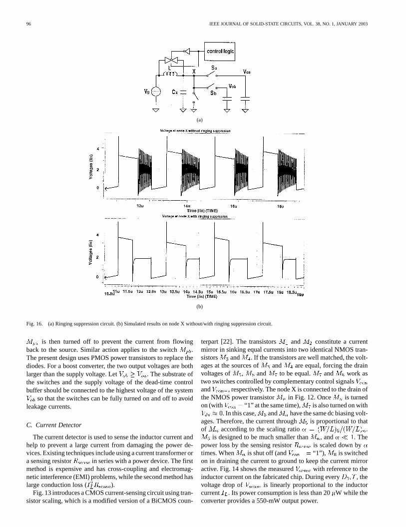
C. Current Detector
The current detector is used to sense the inductor current andhelp to prevent a large current from damaging the power de-vices. Existing techniques include using a current transformer ora sensing resistor in series with a power device. The firstmethod is expensive and has cross-coupling and electromag-netic interference (EMI) problems, while the second method haslarge conduction loss ( ).
Fig. 13 introduces a CMOS current-sensing circuit using tran-sistor scaling, which is a modified version of a BiCMOS coun-
terpart [22]. The transistors and constitute a currentmirror in sinking equal currents into two identical NMOS tran-sistors and . If the transistors are well matched, the volt-ages at the sources of and are equal, forcing the drainvoltages of , and to be equal. and work astwo switches controlled by complementary control signalsand , respectively. The node X is connected to the drain ofthe NMOS power transistor in Fig. 12. Once is turnedon (with “1” at the same time), is also turned on with
. In this case, and have the same dc biasing volt-ages. Therefore, the current through is proportional to thatof according to the scaling ratio .
is designed to be much smaller than , and . Thepower loss by the sensing resistor is scaled down bytimes. When is shut off (and “1”), is switchedon in draining the current to ground to keep the current mirroractive. Fig. 14 shows the measured with reference to theinductor current on the fabricated chip. During every , thevoltage drop of is linearly proportional to the inductorcurrent . Its power consumption is less than 20W while theconverter provides a 550-mW output power.

MA et al.: SIMO SWITCHING CONVERTERS WITH TM CONTROL IN DCM 97
Fig. 17. Chip micrograph.
D. Dead-Time Control
To achieve low on-resistances, the power transistors of theconverter are large. Hence, in Fig. 12 should not be turnedon when either or is conducting to avoid large shoot-through current that would greatly degrade the efficiency andcause large glitches in the inductor current and output voltages.A dead-time control circuitry is, thus, needed [Fig. 15(a)]. Thepower transistors are driven by large buffers. By adding a re-sistor in the driving inverter, the PMOS ( ) of the driven in-verter can be turned off prior to the turn-on of the NMOS ()during a “1” to “0” transition, and shoot-through current of thebuffer can also be avoided. A similar mechanism applies to the“0” to “1” transition. The resistor is realized by and asshown in Fig. 15(a). Fig. 15(b) shows the currents of the invertersimulated by Hspice with and without these delay elements.With the delay elements, only one transistor (NMOS or PMOS)is conducting during logic transitions and no shoot-through cur-rents occurs.
E. Ringing Suppression
Since the converter works in DCM, there are time intervalsthat all power transistors are off. The inductor and theparasitic capacitor then form an oscillatory circuit as shownin Fig. 16(a). Large ringing occurs at node X, causing largeswitching noise and EMI. The present design incorporates aringing suppression circuit [Fig. 16(a)] similar to that discussedin [23]. When all power transistors are off, the inductor isshorted to break the oscillation loop. The voltages at node Xwith and without ringing suppression circuitry are shown inFig. 16(b).
IV. EXPERIMENTAL RESULTS
The SIDO boost converter was fabricated with a standard0.5- m CMOS n-well process. Fig. 17 shows the chip mi-crograph of the converter. Power transistors are connected tomultiple pads in parallel to achieve low parasitic resistance.The NMOS transistor is split into two parts for easyrouting. Fig. 18 shows the inductor current of the converter
Fig. 18. Inductor current of the converter in the steady state.
Fig. 19. Voltage at node X.
Fig. 20. The two outputs with reference to the inductor current.
in the steady state, which correlates well with our simulatedwaveform. Fig. 19 shows the waveform at Node X of theconverter. The duty ratios at alternate cycles are those of theindividual subconverters. When all the switches are off, Node X

98 IEEE JOURNAL OF SOLID-STATE CIRCUITS, VOL. 38, NO. 1, JANUARY 2003
(a)
(b)
Fig. 21. (a) The two outputs with a dynamic load atV . (b) The two outputswith a dynamic load atV .
settles to or quickly and smoothly, demonstrating thatringing due to DCM operation has been effectively suppressed.The two output voltages, 3 and 3.6 V, are shown in Fig. 20with reference to the inductor current. Fig. 21 illustrates thatthe converter is not susceptible to cross regulation. The outputcurrent of subconverter A is 75 mA, and that of subconverterB is 25 mA. An electronic load provided by HP6063B isconnected to the output of subconverter B. The load currentsteps from 0 to 50 mA at a frequency of 1 KHz and a duty ratioof 0.5. The slew rate of the load current is set at 0.083 A/s.Measurement results show that the load change in subconverterB has little effect on the output of subconverter A, and viceversa, thus verifying the analysis in Section II-C. Fig. 21 alsoshows that both outputs could recover to the steady-state valueswithin 250 s. Fig. 22(a) shows that when changes, theinductor current of subconverter A (the lower side of) risesaccordingly, while that of subconverter B (the higher side of
) remains unchanged. The close-up view of Fig. 22(a) isshown in Fig. 22(b) in revealing the changes of the inductorcurrent in detail. A similar testing setup can be used to measureload regulation. Fig. 23 shows the efficiency of the converterversus the two output loads. Although the parasitic resistanceof the inductor is 125 m and the capacitor ESRs are 80 mormore, the converter achieves high efficiency over a wide range.The maximum efficiency 88.4% is measured at mWand mW. As load currents increase, conduction loss
(a)
(b)
Fig. 22. (a) The inductor current with a dynamic load at one output. (b)Close-up view of (a).
Fig. 23. Efficiency of the proposed SIDO converter.
dominates. As load currents decrease, switching loss domi-nates. In both cases, the efficiency drops. Table II summarizesthe performance of the converter.

MA et al.: SIMO SWITCHING CONVERTERS WITH TM CONTROL IN DCM 99
TABLE IIPERFORMANCESUMMARY
V. CONCLUSION
A SIDO boost converter with TM control was presented.Compared to existing designs, the converter requires fewerinductors, power devices, and control loops, which is suitablefor portable applications and system-on-chips (SOCs). Systemimplementation issues were discussed. Experimental resultsdemonstrate the functionality and show good performanceof the design on voltage regulation, power efficiency, andcross-regulation suppression. The SIDO converter provides acost-effective solution in designing on-chip power managementsystems and realizing voltage scheduling techniques.
REFERENCES
[1] J. Rabaey and M. Pedram,Low Power Design Methodologies. Boston,MA: Kluwer, 1996.
[2] Y.-H. Lu and G. De Micheli, “Comparing system level power manage-ment policies,”IEEE Des. Test Comput., vol. 18, pp. 53–60, Mar. 2001.
[3] J.-M. Chang and M. Pedram, “Energy minimization using multiplesupply voltages,”IEEE Trans. VLSI Syst., vol. 5, pp. 436–443, Dec.1997.
[4] T. Ishihara and K. Asada, “A system level memory power optimizationtechnique using multiple supply and threshold voltages,” inProc. Asianand South Pacific Design Automation Conf., Jan. 2001, pp. 456–461.
[5] Y.-J. Yeh, S. Y. Kuo, and J. Y. Jou, “Converter-free multiple-voltagescaling techniques for low-power CMOS digital design,”IEEE Trans.Computer-Aided Design, vol. 20, pp. 172–176, Jan. 2001.
[6] K. Usami, M. Igarashi, F. Minami, T. Ishikawa, M. Kanazawa, M. Ichida,and K. Nogami, “Automated low-power technique exploiting multiplesupply voltages applied to a media processor,”IEEE J. Solid-State Cir-cuits, vol. 33, pp. 463–472, Mar. 1998.
[7] M. Johnson and K. Roy, “Scheduling and optimal voltage selection forlow power multi-voltage DSP datapaths,” inProc. IEEE Int. Symp. Cir-cuits and Systems, vol. 3, May 1997, pp. 2152–2155.
[8] J. Goodman, A. P. Dancy, and A. P. Chandrakasan, “An energy/secu-rity scalable encryption processor using an embedded variable voltageDC/DC converter,”IEEE J. Solid-State Circuits, vol. 33, pp. 1799–1809,Nov. 1998.
[9] M. Brown, Practical Switching Power Supply Design. San Diego, CA:Academic, 1990.
[10] R. W. Erickson,Fundamentals of Power Electronics. Boston, MA:Kluwer, 1999.
[11] A. P. Dancy, R. Amirtharajah, and A. P. Chandrakasan, “High-efficiencymultiple-output dc-dc conversion for low-voltage systems,”IEEE Trans.VLSI Syst., vol. 8, pp. 252–263, June 2000.
[12] D. Ma, W.-H. Ki, C.-Y. Tsui, and P. K. T. Mok, “A 1.8 V single-inductordual-output switching converter for power reduction techniques,” inDig.Tech. Papers IEEE VLSI Symp. Circuits, June 2001, pp. 137–140.
[13] T. Li, “Single inductor multiple output boost regulator,” U.S. Patent6 075 295, June 2000.
[14] D. Goder and H. Santo, “Multiple output regulator with time se-quencing,” U.S. Patent 5 617 015, Apr. 1997.
[15] Y. Ma and K. M. Smedley, “Switching flow-graph nonlinear modelingmethod for multistate-switching converters,”IEEE Trans. Power Elec-tron., vol. 12, pp. 854–861, Sept. 1997.
[16] M. W. May, M. R. May, and J. E. Willis, “A synchronous dual-outputswitching dc-dc converter using multibit noise-shaped switch control,”in Dig. Tech. Papers IEEE Int. Soild-State Circuits Conf., Feb. 2001, pp.358–359.
[17] R. D. Middlebrook and S. Cuk, “A general unified approach to modelingdc-to-dc converters in discontinuous conduction mode,” inProc. IEEEPESC’77, 1977, pp. 36–57.
[18] J. Sun, D. M. Mitchell, M. F. Greuel, P. T. Krein, and R. M. Bass, “Mod-eling of PWM converters in discontinous conduction mode—A reexam-ination,” in Proc. IEEE PESC’98, 1998, pp. 615–622.
[19] V. Tam, “Loop gain simulation and measurement of PWM switchingconverters,” M. Phil. thesis, The Hong Kong Univ. Sci. Technol., HongKong, China, 1999.
[20] D. Ma, W.-H. Ki, C. Y. Tsui, and P. K. T. Mok, “A family of single-in-ductor multiple-output switching converters with bipolar outputs,” inProc. IEEE Int. Symp. Circuits and Systems, vol. 3, May 2001, pp.301–304.
[21] W.-H. Ki and D. Ma, “Single-inductor multiple-output switching con-verters,” inProc. IEEE PESC, vol. 1, June 2001, pp. 226–231.
[22] W.-H. Ki, “Current sensing technique using MOS transistors scalingwith matched bipolar current sources,” U.S. Patent 5 757 174, May 26,1998.
[23] S.-H. Jung, N.-S. Jung, J.-T. Hwang, and G.-H. Cho, “An integratedCMOS DC-DC converter for battery-operated systems,” inProc. IEEEPESC’99, 1999, pp. 43–47.
Dongsheng Ma (S’00) received the B.Sc. degreewith highest honors as an Excellent GraduateStudent and the M.Sc. degree, both in electronicscience, from Nan Kai University, Tianjin, China,in 1995 and 1998, respectively. He is currentlyworking toward the Ph.D. degree at The Hong KongUniversity of Science and Technology, Hong Kong,China.
His research interests include integrated powermanagement system designs, low-voltage analogand mixed-signal integrated circuit designs, control
methodology, and modeling of power electronics systems.Mr. Ma is a recipient of an STMicroelectronics Ltd. Scholarship, Motorola
Ltd. Scholarship, Guang Hua Foundation Scholarship, and Hua Wei Scholarshipfor academic and research excellence. He also won a Distinguished Paper Awardin the IEEE (Hong Kong) 2000 Student Paper Contest.

100 IEEE JOURNAL OF SOLID-STATE CIRCUITS, VOL. 38, NO. 1, JANUARY 2003
Wing-Hung Ki (S’86–M’92) received the B.Sc. de-gree from the University of California, San Diego, in1984, the M.Sc. degree from the California Instituteof Technology, Pasadena, in 1985, and the Engineerand Ph.D. degrees from the University of California,Los Angeles, in 1990 and 1995, respectively, all inelectrical engineering.
He joined Micro Linear Corporation, San Jose,CA, in 1992, as a Senior Design Engineer in theDepartment of Power and Battery Management,working on the design of power converter con-
trollers. He then joined The Hong Kong University of Science and Technology,Hong Kong, China, in 1995, where he is currently an Associate Professor inthe Department of Electrical and Electronic Engineering. His research interestsinclude design and modeling of switch-mode power converters, charge pumps,low dropout regulators, switched-capacitor circuits, and analog decodingcircuits.
Dr. Ki was the recipient of the Asia Innovator Award of the Year 1997–1998granted by EDN Asia.
Chi-Ying Tsui (M’95) received the B.S. degree inelectrical engineering from the University of HongKong, Hong Kong, China, in 1982, and the Ph.D. de-gree in computer engineering from the University ofSouthern California, Los Angeles, in 1994.
In 1994, he joined the Department of Electricaland Electronic Engineering, The Hong KongUniversity of Science and Technology, Hong Kong,China, where he is currently an Associate Professor.His research interests focus on designing VLSI ar-chitectures for high-speed networks and low-power
multimedia and wireless applications, designing power management circuitsand techniques for embedded portable devices, and developing VLSI CADalgorithms for low-power applications.
Dr. Tsui received the Best Paper Award from the IEEE TRANSACTIONS ON
VERY LARGE SCALE INTEGRATION (VLSI) SYSTEMS in 1995 and supervisedthe Best Student Paper Award of the 1999 IEEE ISCAS. He has served on thetechnical program committee of a number of conferences and symposiums, in-cluding ILSPED, ASP-DAC, and the IEEE VLSI Symposium.
Philip K. T. Mok (S’86–M’95–SM’02) received theB.A.Sc., M.A.Sc., and Ph.D. degrees in electricaland computer engineering from the University ofToronto, Toronto, ON, Canada, in 1986, 1989, and1995, respectively.
While at the University of Toronto, he was aTeaching Assistant in both the Electrical Engineeringand Industrial Engineering Departments from 1986to 1992. He taught courses in circuit theory, ICengineering, and engineering economics. He wasalso a Research Assistant in the Integrated Circuit
Laboratory, University of Toronto, from 1992 to 1994. In January 1995, hejoined the Department of Electrical and Electronic Engineering, The HongKong University of Science and Technology, Hong Kong, China, as an AssistantProfessor. His research interests include semiconductor devices, processingtechnologies and circuit designs for power electronics and telecommunicationsapplications, with current emphasis on power integrated circuits, low-voltageanalog integrated circuits, and RF integrated circuits design.
Dr. Mok received the Henry G. Acres Medal, the W.S. Wilson Medal, and aTeaching Assistant Award from the University of Toronto, and the Teaching Ex-cellence Appreciation Award twice from The Hong Kong University of Scienceand Technology.