Embed Size (px)
Citation preview

Simulation Researches on Feed Method of GSM Microstrip Antenna
for Impedance Match
Abstract—In present work, the feed method of GSM
microstrip antenna for impedance match was studied. Firstly,
Transmission Line Model (TLM) and impedance theory were
introduced. Using three-dimensional electromagnetic
simulation software ANSYS Ansoft HFSS, the effects of
different feed points on the E-plane and H-plane pattern were
studied for the GSM probe-fed microstrip antenna. Moreover,
the variation tendency of the reflection coefficient of antenna
with the frequency varying from 900 to 1000 MHz was
discussed. The simulation results could not merely present
directive significance to the suitable match between microstrip
antenna and feed lines, but also contribute to the improvement
of transmission efficiency and the acceleration of design cycle.
Keywords-microstrip antenna; input impedance; feed method
I. INTRODUCTION
As a major medium for information transmission, antennas were vital and indispensable parts in the field of wireless communication. Portable wireless communication devices, such as codeless telephone, personal communica-tion service (PCS), cellular telephone, radio modem, etc., usually were quite close to human body when working, and therefore some requirements were put forward on antenna, i.e., the imposed effects and the absorbed radiation should be minimized as much as possible, both of which could be satisfied to the fullest extent by the microstrip antenna, mainly owing toits good integration properties, specifically, the capability to be assembled internally. Microstrip antenna could be integrated to printed circuit board (PCB) or the case without any increase of device dimension, with the obtained built-in antenna being of high mechanical strength, good fracture resistance performance, little imposed impacts of human activities and no need to be pulled out when used. Moreover, the transresistance could be reduced to the greatest degree with the employment of high-level shielding technology. In the 21-st century, the worldwide rapid development of personal communications have largely motivated the boom of studies on microstrip antenna, in which analysis on the impedance characteristics remained as one of the key problems. For a specially-selected communication antenna, the perception of impedance characteristics within the working frequency band was
indispensable, by which the proper design of matching circuits or the favorable feed method could be obtained with the purpose to solve the matching problem between the antenna and feed line, and finally effective transmissions and emissions were achieved.
Due to it slight weight, small volume and flimsy section, microstrip patch antenna could be produced together with feed line and matching circuits simultaneously, which also could be integrated with the PCB in the communication system. The microstrip patch could be produced following designed process, with low cost and easy in mass production, making them widely adopted in GSM communication system. In present work, using the antenna simulation software, the effects of different feed points on the pattern and corresponding impedance characteristics of antenna were investigated for the probe-fed microstrip antenna, by which the matching feed and effective emission were achieved.
II. PRINCIPLE AND RADIATION FIELD OF MICROSTRIP
ANTENNA
In spite of the short history, the microstrip antenna has attracted great attentions on account of its several advantages, and a lot of works have been carried out by researchers, by which various theories and analytic techniques on microstrip antenna were proposed. In general, three theoretical models were adopted, which would be elaborated as follows. In Transmission Line Model (TLM) theory, rectangular microstrip patch antenna was taken as a length of microstrip transmission lines, with both two ends loaded by the equivalent admittance of radiating slot. However, TLM theory was only applicable to thin rectangular patch antenna basically. As proposed by Prof. Luo, the lower space of thin microstrip antenna in Cavity Model (CM) theory could be regarded as a resonator cavity, which was composed of upper and bottom electric walls and peripheral magnetic wall. With the employment of CM theory, an in-depth perception on the performance characteristics of microstrip antenna could be obtained, and the input impedance of the antenna with the thickness
ranging from 0.005 g ~ 0.02 g could be calculated. CM
theory could be used in the discussion of patch antennas with different shapes; however, the model was restricted to the situation that far less antenna thickness compared with
Ye Jian-wei
PLA South China Service Center for
Computer Technology
Guangzhou 510502, China
e-mail:[email protected]
Ye Jiang-fang
College of Information Science and
Technology
Donghua University, No. 2999 North
Remin Road,
Shanghai 201620, China
e-mail:[email protected]
Tu Jia-le
PLA South China Service Center for
Computer Technology
Guangzhou 510502, China
e-mail:[email protected]
International Conference on Computer Science and Service System (CSSS 2014)
© 2014. The authors - Published by Atlantis Press 573

the wavelength. IEM-Integral Equation Method (IEM) theory, also known as Full Wave theory, was a numerical solution problem based on the electromagnetic boundary conditions. In principle, IEM theory could be applicable to the microstrip antennas with different structures and thicknesses; nevertheless, it would suffer many limitations in practical, such as calculated models and time.
For the rectangular patch adopted in present work, TLM could be considered as the ground mode in CM theory. The calculated field distribution and related parameters approached the practical results at around the resonant frequency, which could meet the engineering accuracy on the whole. In TLM theory, the fundamental ideas were that the rectangular patch was considered as a section of low-resistance transmission lines and the two equivalent slots for two ends of patch were considered as the physical model displayed in Fig. 1.
As shown in Fig. 1, the dimension of rectangular microstrip patch was L*W, with the thickness of substrate
being h; specifically, 0 , where 0 represented the wave
length in free space. The patch mentioned above could be considered as a section of microstrip communication line, with the length and width being L and W, respectively. Open circuit appeared near the terminal end along L side, and therefore the voltage antinode formed. In general, L could
be set as 2
gL approximately, while another antinode
appeared at the other terminal end along L side. The radiation of antenna could be corresponding to a dual-slot radiation, and the equivalent magnetic current across the slot was uniform, by which the radiation field of antenna could be calculated
E =Acos cos 0[ sin cos ]2
K L
F1(θ, ) F2(θ, ) (1)
in which F 1 (θ, )=
0
0
sin[ sin sin ]2
sin sin2
K W
K W,
F2(θ, )=
0
0
sin[ sin cos ]2
sin cos2
K h
K h, A= 0 '
'
2
jk r
g
VWj e
r, and
'r
was the distance between a certain point in field and the central point of patch.
As mentioned before, h<< g , F2(θ, ) were
approximately to be 1 and Eq. (1) could be rewritten as
E =Acosθsin cos 0[ sin cos ]2
K L
F 1 (θ, ).
It could be deduced from above two equations that: (i) if
=0°,E component existed, which could be considered
as E plane, including the propagation direction of
quasi-TEM wave and z axis; (ii) if =0°, E was zero and
only E component existed, which also known as H plane,
being perpendicular to the direction of propagation. Accordingly, the normalized pattern of E plane when
=0° could be described as: 0( ) cos[ sin ]2
E
Lf k ; while
the normalized pattern of H plane when =90° could be
described as0
0
sin [ sin ]cos2( )
sin2
H
Wk
fW
k
.
The corresponding radiation power could be expressed as:
*1
2
s
P E H r ds (2)
III. RESEARCHES ON FEED METHOD AND IMPEDANCE
CHARACTERISTICS OF MICROSTRIP ANTENNA
As one kind of energy converters, transmitting antenna converted the high frequency current (HFC) into the radiation electromagnetic field energy, i.e., spatial electromagnetic wave, while receiving antenna performed are verse procedure. Either the connection between transmitter and antenna or the connection between antenna and receiver were implemented by feed lines, which implied that matching performance between antenna and feed lines would directly affect the effectiveness of transmitting and receiving of antenna. Only when matched with the input impedance of antenna acceptably, the feed lines worked in the traveling wave regime and yielded efficient transmission and emission of current. Consequently, studies on the feed method and impedance characteristics of antenna were necessary and significant.
Fig. 1 The schematic diagrams for the structure of rectangular microstrip patch antenna and physical model of TLM theory.
574
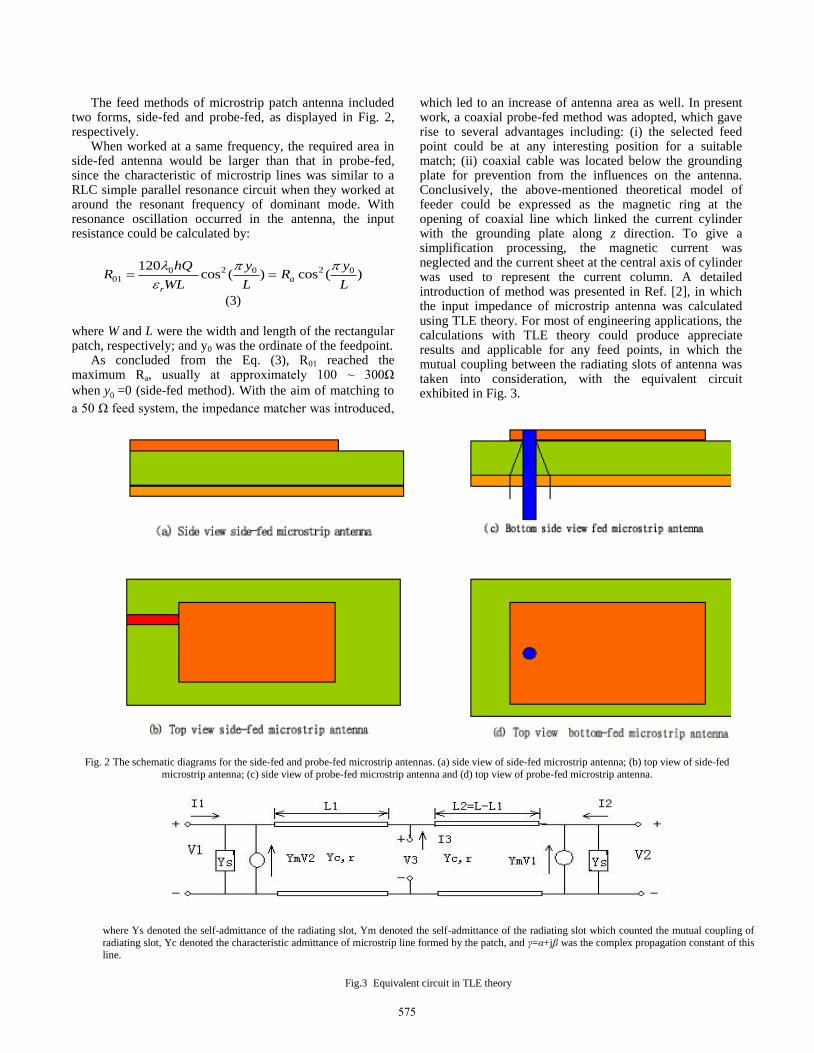
The feed methods of microstrip patch antenna included two forms, side-fed and probe-fed, as displayed in Fig. 2, respectively.
When worked at a same frequency, the required area in side-fed antenna would be larger than that in probe-fed, since the characteristic of microstrip lines was similar to a RLC simple parallel resonance circuit when they worked at around the resonant frequency of dominant mode. With resonance oscillation occurred in the antenna, the input resistance could be calculated by:
2 20 0 001
120cos ( ) cos ( )
a
r
hQ y yR R
WL L L
(3)
where W and L were the width and length of the rectangular patch, respectively; and y0 was the ordinate of the feedpoint.
As concluded from the Eq. (3), R01 reached the maximum Ra, usually at approximately 100 ~ 300Ω
when 0y =0 (side-fed method). With the aim of matching to
a 50 Ω feed system, the impedance matcher was introduced,
which led to an increase of antenna area as well. In present work, a coaxial probe-fed method was adopted, which gave rise to several advantages including: (i) the selected feed point could be at any interesting position for a suitable match; (ii) coaxial cable was located below the grounding plate for prevention from the influences on the antenna. Conclusively, the above-mentioned theoretical model of feeder could be expressed as the magnetic ring at the opening of coaxial line which linked the current cylinder with the grounding plate along z direction. To give a simplification processing, the magnetic current was neglected and the current sheet at the central axis of cylinder was used to represent the current column. A detailed introduction of method was presented in Ref. [2], in which the input impedance of microstrip antenna was calculated using TLE theory. For most of engineering applications, the calculations with TLE theory could produce appreciate results and applicable for any feed points, in which the mutual coupling between the radiating slots of antenna was taken into consideration, with the equivalent circuit exhibited in Fig. 3.
Fig. 2 The schematic diagrams for the side-fed and probe-fed microstrip antennas. (a) side view of side-fed microstrip antenna; (b) top view of side-fed
microstrip antenna; (c) side view of probe-fed microstrip antenna and (d) top view of probe-fed microstrip antenna.
where Ys denoted the self-admittance of the radiating slot, Ym denoted the self-admittance of the radiating slot which counted the mutual coupling of
radiating slot, Yc denoted the characteristic admittance of microstrip line formed by the patch, and γ=α+jβ was the complex propagation constant of this
line.
Fig.3 Equivalent circuit in TLE theory
575

As displayed in Fig. 3, the admittance matrix of three-port network could be described as:
With the regard to the system fed by radiation side, i.e.,
I 2 =I 3 =0, L 3 =0, and then
21
1
[ csc ( )]coth( )
coth( )
m cin s c
s c
Y Y h LIY Y Y L
V Y Y L
2 2 21
1
2 coth( ) 2 csc ( )
coth( )
c s m c s c min
s c
Y Y Y Y Y L Y Y h LIY
V Y Y L
For the systemfed by any feed points, the ports were adopted as the feed point, and then
21
1
[ csc ( )]coth( )
coth( )
m cin s c
s c
Y Y h LIY Y Y L
V Y Y L
2 2 21
1
2 coth( ) 2 csc ( )
coth( )
c s m c s c min
s c
Y Y Y Y Y L Y Y h LIY
V Y Y L
When fed by probe, the inductance of lead wire should be added to the input impedance, which could be calculated approximately by the probe reactance of the dielectric-filled parallel-plate waveguide. Assumed that the thickness of probe was d0, and then
X L = 0
0 0
377ln
r
h
d (5)
where Z c = 0
ee
h
W; = 0
2
g
k e , g = 0
e
,
α=0.5βtane , 0 =120 , representing the wave impedance
in free space; 0k = 2 / 0 , representing the wave number in
free space; 1/21 10[ 1 ( 1)(1 ) ]
2 e r r
h
W, representing
the corresponding dielectric constant; tan e was the
equivalent tangent value of losses; eW was the equivalent
width, i.e., eW =W+ l , W was the actual width and l
could be calculated by Hamosita’s empirical formula:
l
h=0.412
( 0.3)( / 0.264)
( 0.258)( / 0.8)
e
e
W h
W h (6)
The relationship between the calculation of parameters in admittance matrix and the above-described radiation field of antenna was depicted minutely in Ref. [4].
IV. ANALYSES ON THE FUNDAMENTAL
CHARACTERISTICS OF PROBE-FED MICROSTRIP ANTENNA
WITH ANSOFT HFSS
Taken a fan-beam base station antenna for example, the effects of the variation of feed point on the input impedance and pattern of antenna were studied using three-dimensional electromagnetic simulation software ANSYS Ansoft HFSS, by which the feed point would be selected properly to produce a satisfactory match between microstrip antenna and feed lines.
The related parameters in the system were listed as follows. The dimension of antenna was 46 mm * 50 mm * 2.5 mm, and the substrate was composed of PTEE glass fiber, with the dielectric constant εr being 2.55 and
conductivity C being 104 s/mm. The antenna worked in
the TM01 mode, and the field exhibited an even distribution along X direction and a varied distribution along Y direction meanwhile. Along the Y direction, the feed point was shifted at about 5, 15, 20 and 25 mm, and the corresponding variation tendency of input impedance and pattern of antenna would be discussed deeply in the following.
As illustrated in Figs. 5-8, the E-plane and H-plane patterns
with the selection of different feed points were displayed in
(a) and (b), respectively; and the variations of reflection
coefficient of antenna with the change of frequency at
different feed points, with the frequency varying from 900
to 1000 MHz were given in (c). As a single-port network,
the reflection coefficient of antenna presented a one-to-one
correspondence relationship with the input impedance: _
11
11
1
1
SZ
S.
Fig. 4 The schematic diagram of the feed-point position.
(1)X=21mm, Y=0.1L =5mm
(2)X=21mm, Y=0.3L=15mm
(3)X=21mm, Y=0.4L=20mm
(4)X=21mm, Y=0.5L=25mm
576

(a) (b) (c)
Fig. 5 The variations of pattern and reflection coefficient 11S whenY=0.1L=5mm.
(a) (b) (c)
Fig. 6 The variations of pattern and reflection coefficient 11S whenY=0.3L=15mm.
(a) (b) (c)
Fig. 7 The variations of pattern and reflection coefficient 11S whenY=0.4 L= 20 mm.
(a) (b) (c)
Fig. 8 The variations of pattern and reflection coefficient 11S whenY=0.5 L= 25mm.
577

V. CONCLUSIONS
From the simulation results in Figs. 5-8, some main conclusions could be drawn and listed as follows:
(i) As shown in (c) of Figs. 5-8, the input impedance of antenna presented a variation to a large degree with the shift of feed point along Y direction. The reflection coefficient in Fig. 7 (c) almost approached the circle of pure reactance, resulting in a severe mismatch. It could be found in Fig. 6 (c) that frequency range located in the circle of equal standing wave was the biggest, which implied that an excellent match state was obtained and therefore provided theoretical basis for the suitable selection of feed point.
(ii) The pattern of antenna mainly depended on the dominant mode field, which remained almost invariable with the change of feed-point position, as shown in the (a) and (b) of Figs. 5-7. Nevertheless, the feed point could not be selected at around Y = 0.5 L, since the related reflection
coefficient would be at the unit circle, i.e., 11 1s , implying
a serious mismatch. Meanwhile, the pattern displayed an awful distortion, which could not meet the requirements in normal communications.
In summary, using Ansoft HFSS simulation software, the pattern and reflection characteristics of GSM microstrip antenna with the selection of different feed points were investigated, and the degree of impedance match in a specified range of working frequency was studied, which would provide directive significance to the achievement of the match between GSM microstrip antenna and feed lines, the improvement of transmission efficiency and reduction of the design circle of antenna.
REFERENCES
[1] J. Zhang, K. C. Liu, C. J. Hao, Theory and Engineerings of Microstrip Antenna, 1988, National Defense Industry Press, Beijing.
[2] S. S. Zhong, Theory and Application of Microstrip Antenna, 1991, pp. 128-230. Xidian University Press, Xi’an.
[3] I.J.Garg Ramesh and P. Bhartia ,Microstrip Antenna Design Handbook, 2001,Artech House ,Boston.London.
[4] H. Pues and A. Van de Capelle. Accurate Transmission-line Model for the Rectangualr Microstrip Antenna [J]. IEE Proc. H, Vol.131, Dec. 1984, 334-340
[5] W. L. Stutzman and G. A. Thiele, Antenna Theory and Design, Post & Telecom Press, Beijing, 2006.
AUTHORS’ DESCRIPTION
Ye Jian-wei, was born in Lanxi City, Zhejiang Province, China, in 1963. As a Master of Engineering, he is a senior engineer. His research interests are focused on the system structure of communication and computers, whose research projects have received the scientific and technology progress awards several times.
Ye Jian-fang, was born in Shanghai City, China, in 1964. As a master of science, she is an associate professor. Her research interests are focused on the wireless communica-tion and network technology of RF circuit, whose research projects have received the teaching achievements and scientific and technology progress awards several times.
TuJia-le, was born in Changsha City, Hunan Province, China, in 1981. As a Master of Engineering, he is a lecturer. With the research interests being focused on the software engineering of communication and computers, he has taken part in many scientific research projects at provincial and ministerial level.
578