Embed Size (px)
Citation preview

SIMD Microprocessor for Image Processing
Timothy Forrest - 20515848
School of Electrical, Electronic and Computer Engineering University of Western Australia
Supervisor Prof. Thomas Bräunl
Professor of School of Electrical, Electronic and Computer Engineering University of Western Australia
30 May 2014

Abstract Digital images are merely matrices, with each element representing a single pixel. There are
many image processing routines that consist of performing the same operation on each pixel
of an image, such as brightness adjustments and edge detection. Performing the same
operation on large sets of data is exactly what parallel processing is great for, allowing huge
increases in performance. This project examined the use of a Single Instruction Multiple Data
(SIMD) microprocessor for the parallel processing of images. The SIMD microprocessor as
the name suggests is designed to perform a single instruction on any amount of data (for each
pixel in this case) in a single operation cycle.
The design and preliminary simulation of the SIMD microprocessor was done using Retro, a
graphical circuit design tool. Retro had to first be further developed and improved to allow
the simulation of an SIMD microprocessor. The circuit was then developed and simulated, a
number of image processing routines were simulated to show the performance gains over a
non-parallelised processor. Retro was also extended to allow the generation of VHDL from
the graphical circuit. VHDL stands for VHSIC Hardware Description Language and is a
coding language used for electronics design. The VHDL for a single Processing Element has
been generated and tested, however the VHDL generation for the entire SIMD system still
requires further work. Once the VHDL generation is complete the full circuit can be
synthesised and simulated and finally implemented on a Field-programmable gate array
(FPGA) in the future.

Acknowledgements I would like to acknowledge and thank the following persons for their contributions and guidance in completing this project:
Prof. Thomas Braunl, my supervisor - for making this project possible, the guidance he gave and his input into the direction of this project.
Adrian Boeing, my temporary supervisor for the second half of my project, for his suggestions and support.
Zhiqiang Qiu, my project partner - for all his contributions to this project.

Contents Abstract ...................................................................................................................................... 3
Acknowledgements .................................................................................................................... 4
Nomenclature ............................................................................................................................. 7
1. Introduction ............................................................................................................................ 8
1.1 Motivation ........................................................................................................................ 8
1.2 Objective .......................................................................................................................... 9
1.3 Outline.............................................................................................................................. 9
2. Background & Related Work............................................................................................... 10
2.1 Digital Images ................................................................................................................ 10
2.2 SIMD.............................................................................................................................. 12
2.3 Retro ............................................................................................................................... 13
2.4 Related Work ................................................................................................................. 14
3. Retro ..................................................................................................................................... 16
3.1 Retro Overview .............................................................................................................. 16
3.2 Retro ............................................................................................................................... 17
3.2.1 Interface .................................................................................................................. 17
3.2.2 Circuit Files ............................................................................................................. 18
3.2.3 Components ............................................................................................................ 18
3.2.4 Simulation ............................................................................................................... 19
3.3 Modular Design ............................................................................................................. 20
3.3.1 Module Concept & Components ............................................................................ 20
3.3.2 Module Simulation.................................................................................................. 22
3.3.3 VHDL Generation ................................................................................................... 23
4. SIMD Image Microprocessor Design .................................................................................. 25
4.1 SIMD Design Overview ................................................................................................ 25
4.2 Sequencer CPU .............................................................................................................. 27
4.2.1 Sequencer CPU - ALU............................................................................................ 29
4.2.2 Sequencer CPU - Control Unit ............................................................................... 30
4.2.3 Instructions & Sequencer Op Codes ....................................................................... 31
4.2.4 Status Register ........................................................................................................ 33
4.2.5 Clock ....................................................................................................................... 34
4.2.6 Memory ................................................................................................................... 34

4.2.7 Program Flow.......................................................................................................... 35
4.3 Processing Element Design............................................................................................ 36
4.3.1 PE Design - ALU .................................................................................................... 40
4.3.2 PE Design - Status Register .................................................................................... 41
4.3.3 PE Design - Activity Register ................................................................................. 42
4.3.4 PE Design - Memory .............................................................................................. 47
4.3.5 PE Design - Interconnections.................................................................................. 47
4.3.6 PE Design - PE Instruction Set ............................................................................... 48
5. SIMD Image Processing ...................................................................................................... 49
5.1 Summation ..................................................................................................................... 50
5.2 Thresholding .................................................................................................................. 52
5.3 Nested-If ........................................................................................................................ 54
5.4 While Loop .................................................................................................................... 56
5.5 Increase Image Brightness ............................................................................................. 58
5.6 Sobel Edge Detection ..................................................................................................... 60
6. VHDL Simulation ................................................................................................................ 64
6.1 PE Simulation ................................................................................................................ 64
6.1.1 Addition .................................................................................................................. 65
6.1.2 Activity Register ..................................................................................................... 66
6.1.3 Load from Memory ..................................................................................................... 66
7. Conclusion ........................................................................................................................... 68
7.1 Future Work ................................................................................................................... 69
References ................................................................................................................................ 70
Appendices ............................................................................................................................... 71
Appendix 1.0 - SimulationEngine Class Excerpt ................................................................ 71
Appendix 1.1 - Module Drawing ......................................................................................... 71
Appendix 1.2 - Module Setup & Loading ........................................................................... 73
Appendix 2.0 - VHDL for PE .............................................................................................. 80

Nomenclature SIMD Single Instruction Multiple Data
VHDL VHSIC Hardware Description Language
FPGA Field-programmable gate array
SISD Single Instruction Single Data
MISD Multiple Instructions Single Data
MIMD Multiple Instructions Multiple Data
AWT Abstract Window Toolkit
PE Processing Elements
CPU Central Processing Unit
ALU Arithmetical Logic Unit
ACCU Accumulator
PC Program Counter
LSB Least Significant Bit
HEX Hexadecimal
BRR Branch on Ready
Retro Register-Transfer Object Hardware Simulation

1. Introduction
1.1 Motivation Image processing is a very large field with endless real world applications. Face recognition,
object tracking and image restoration are all examples of image processing applications. The
majority of image processing applications are however based on relatively simple operations
performed on a large amount of data. The amount of data is ever increasing as the resolution
(size) of images capable of being captured by modern digital cameras is always increasing.
The hardware required to process images from modern cameras does exist. However there are
many applications that require the use of a microprocessor to perform image processing. The
main advantage of microprocessors is the mobility they provide due to their reduced size and
power consumption compared with standard processing units. There are modern
microprocessors that can already handle some image processing. However the current
generation of general purpose microprocessors do not offer the performance required to
process large images quickly. Therefore there is a need for a dedicated image microprocessor
capable of processing large images very quickly. Fast processing of larger (higher resolution)
images allows increased accuracy in applications such as object tracking and facial
recognition, as well as enabling the use of real-time image processing.
A dedicated image microprocessor can be much simpler than a general purpose
microprocessor while having the processing power necessary for fast image processing.
There are many ways of increasing processing power however the most efficient for image
processing is the addition of parallel processing. Image processing relies on performing the
same operation on a large number of data elements, hence it is highly parallelisable. One
approach to parallelisation is Single Instruction Multiple Data (SIMD) architecture. This
architecture allows any number of parallel processing elements to be harnessed to vastly
increase the performance of image processing routines.
Using a graphical logic simulator to design the SIMD system offers great usability and
flexibility. The system can be quickly prototyped and modified to perform as needed. The
additional challenge when simulating an SIMD system is that the simulator software has to be
able to handle modular design. There are a number of commercial products that are capable
of these tasks however these are generally expensive and unnecessarily complex for the
design of relatively simple systems. Retro is a logic simulator developed at the University of
Western Australia (UWA). It was not originally developed to handle SIMD systems however

the source code is freely available to allow extensions. Retro is used as a teaching tool at
UWA so any extensions made would also benefit future student users. This was the main
reason for choosing to extend Retro as opposed to using existing software packages.
1.2 Objective This project has two main focuses; the design of an SIMD microprocessor for image
processing and, the improvement and extension of Retro. The SIMD microprocessor was
designed to meet two primary goals, provide highly parallelised computational power for
high performance image processing and be as simple as possible to minimise the number of
gates needed (hence minimising size). The SIMD design was achieved by utilising the
additions made to Retro.
The extensions made to Retro revolved around two major additions. Firstly was the ability to
modularise designs, this would allow existing circuits to be represented as 'modules' in
another circuit. Secondly was the ability to generate VHDL from the graphical circuit in
Retro. The main goal for the VHDL was to have the behavioural simulation of the generated
VHDL to be as close as possible to matching the logical simulation performed within Retro.
This would ensure the design in Retro was translated into VHDL correctly. Synthesising the
generated VHDL would require platform-dependent changes and hence was not a primary
objective in the VHDL generation. The changes required to synthesis the generated VHDL
have to be implemented by the user. Along with these changes a number of fixes and
improvements were required for Retro.
1.3 Outline The project was broken down into the following stages:
1. Retro - addition of modular design capabilities
2. SIMD - design & simulation of the SIMD microprocessor in Retro
3. Retro - addition of VHDL generation capabilities
4. SIMD - behavioural simulation of VHDL generated for SIMD microprocessor
Further background and a look into related work already carried out in this area will be
provided in Chapter 2. The Retro additions, covering stages 1 & 3 above will be examined in
Chapter 3. Chapters 4 & 5 will look at the design of the SIMD microprocessor and its
simulation (both in Retro and VHDL) respectively. Finally the results of the SIMD design
and the Retro additions will be summarised in Chapter 6.

2. Background & Related Work
2.1 Digital Images Digital images are essentially a simple 2D matrix of constant values. Each element in this
matrix is simply a numerical constant indicating the intensity, for example 0 - 255 when
using an 8-bit intensity. Colour images simply have 3 matrices, one for each colour channel,
for example RGB has a red, green and blue matrix again containing intensities in each matrix
element. The combination of these three separate matrices allows for a possible 24 million
different colours to be produced using 8-bit intensities.
Original Image
8x Magnification
Red Green Blue
Figure 1 - Digital Image Breakdown
Figure 1 shows the breakdown of a digital image. The original image can be seen at the top,
this is then put under 800% magnification which allows each individual pixel to be
distinguished. This is then split into the three separate RGB channels. Each of the three RGB
matrices is a matrix with a 0-255 value in each cell as mentioned before, with 0 represented
by black and 255 represented by white. Having established that digital images are simple
matrices this now leads into why parallel processing is so powerful for image processing.

The majority of image processing routines consist of performing a few simple operations on
each pixel value in the image matrix. The key is that we are performing the same operation
over and over for each pixel. This is where parallel processing excels. By using multiple
processing elements to perform the same operation in parallel, the time taken to process a
large set of data (in this case pixels) can be drastically reduced.
Figure 2 shows a 11x11 8-bit greyscale image, the power of parallel processing can be shown
by examining the number of operations required to brighten this image using an SIMD
microprocessor and a traditional single core processing unit.
Figure 2 - Brightening Example
For a traditional processor with a single execution thread, the operations have to be done
sequentially, for simplicity assume a single operation is carried out for each pixel. This
equates to 121 operation cycles. Taking an SIMD microprocessor with 11 processing
elements, the number of operation cycles for the same procedure is only 11. Although this a
very simplified example the huge reduction in operation cycles required can be seen. Most
SIMD microprocessors will have many more processing elements than demonstrated in this
example, thus will have a significant improvement in performance.
2.2 SIMD SIMD architecture is one of the four computer architectures under the classification known as Flynn's taxonomy [1]. The four architectures are:
Single Instruction Single Data (SISD) - All instructions are carried out sequentially with a single control unit and single processing element.
Single Instruction Multiple Data (SIMD) - Single control unit provides same instructions to any number of processing elements, which then carry out the operations in parallel.
Multiple Instructions Single Data (MISD) - Multiple instructions carried out on a single data element.
Multiple Instructions Multiple Data (MIMD) - Multiple different instructions carried on multiple data elements in parallel.
Single Instruction Multiple Instruction Single Data SISD MISD
Multiple Data SIMD MIMD Figure 3 - Flynn's taxonomy
Image processing is about performing the same operation on a large number of data elements, as mentioned before. SIMD is therefore the perfect architecture for the task. Figure 4 gives an overview of how SIMD works.
Processing Element
DATA
INSTRUCTIONSINSTRUCTIONS
Processing Element
.......Processing
Element
Figure 4 - SIMD Overview
There are two main components to the SIMD system; the Control Unit which provides the
instructions and the Processing Elements that carry out the instructions. The design of both is
important to maximise performance and there has already been a number of SIMD
microprocessors designed for image processing which will be examined in section 2.4.

2.3 Retro Retro is an open source graphical logic simulator that was originally developed in 1999 at
UWA. It is a powerful teaching tool as it is quick and easy to use. Logic gates (and, or etc)
and more complex devices (multiplexors, registers etc) are placed using a drag-and-drop
interface, as shown in Figure 5.
Figure 5 - Retro Interface
Once the designs are laid out in Retro they can be simulated using a simple time-step
simulation. The propagation of signals can be viewed at any user chosen time and are
displayed visually within the circuit, with single bit lines using colours to display their
relative value and a simple display component being used to display the value of buses as
shown in Figure 6.
Figure 6 - Retro Simulation

2.4 Related Work The concept of SIMD has been around for a long time and nearly all modern processors have
some variation of SIMD capability. There has been a lot of research into SIMD over the
years. SIMD was used in some of the first attempts at building massively parallel
supercomputers. The ILLIAC IV was the first attempt at creating a supercomputer using
SIMD technology[2]. The ILLIAC IV was however unfortunately not a great success, with
cost blowouts, it ended up only having 64 processing elements versus the original 256 it was
planned to have[3]. It did however show the potential of parallel processing and helped spark
more research into this field. There were a few more SIMD supercomputers built such as the
Connection Machine which saw some degree of success [4]. However with the rise of
inexpensive MIMD processors, supercomputers moved away from SIMD architecture.
SIMD was still being utilised, however now for more specific applications. Intel began
including SIMD technology in their Pentium® processors in 1997 when they introduced the
MMX™ technology [5]. This was an example of an SIMD unit attached to a general purpose
processor to enable high performance multimedia processing. There has also been a number
of SIMD microprocessors designed for image processing dating back to 1990 and even
earlier. In 1990, Athertorn proposed the use of multiple SIMD 'clusters' to form a MIMD
array for real-time image processing [6]. Since then there have been many more SIMD based
image processors designed for various purposes.
One point of differentiation between the proposed designs over the recent years is how the
processing elements (PEs) were designed. Some designs revolve around having small PEs
meaning a large number could fit on a single chip, for example Kurafuji et al. proposed the
MX-2 Core with up to 2048 4-bit PEs per unit [7]. Whereas more general purpose SIMD-
based machines with large PEs have also been shown to provide good performance such as
the Ambric parallel processing array with 336 32-bit processors examined by Osorio et al in
2009 [8]. This project looked at designing processing elements with a select number of
advanced features that have not been implemented in previous work, such as the ability for
PEs to handle nested conditional statements and conditional loops while striving to keep each
PE as small as possible.

The network layout of the PEs is important to how the system works. There has been some
research into different layouts. The two dimensional mesh network, also known as a NEWS
grid, seen in figure 7 is the most common. Other networks such as shuffle-exchange networks
and binary n-cubes offer performance gains in some applications [9]. The two dimensional
mesh was the chosen network layout for this project.
Figure 7 - 2D Mesh Network
The NEWS grid allows each PE to transfer data between its North, East, West and South
neighbours [10]. This again allows for gains in performance for image processing and will be
explained in detail in Chapter 4.

3. Retro
3.1 Retro Overview Retro is a Java based open-source graphical logic simulator as mentioned in Chapter 2. It uses
a drag-and-drop interface to place components, which are contained within a 'Library'. Each
component contains information on its simulation model, connections and how to display it.
Once components are placed, they are joined by wires (a single bit) or buses (collection of
bits). Finally the circuit can be simulated using the simulation controls which consist of Stop,
Go, Step and Pause functions. Throughout the simulation the signals are shown graphically
on the circuit.
Retro was suited well to the creation of a relatively simple system such as the SIMD
microprocessor. However it did lack features necessary for the design to be completed
efficiently and effectively. The addition of the ability to modularise designs was required and
is discussed in Section 3.3. The other major addition was the ability to generate VHDL
directly from the graphical circuit in Retro, this is discussed in detail in Section 3.4. Firstly
however it is necessary to look at how the code behind Retro works, this can be split up into
the Interface, Circuit files, Components & Simulation.
3.2 Retro
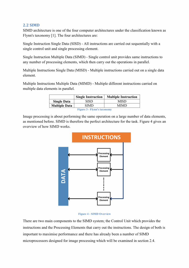
3.2.1 Interface The Retro interface is implemented using the Java Abstract Window Toolkit (AWT)
framework [11]. It consists of a Menu bar, a Tool bar, Component Selection bar and the
Working area.
Figure 8 - Retro Interface
The interface was first designed in 1999 so there are many features expected in modern
software that are not present, such as keyboard shortcuts and Undo/Redo. The main issue
with the current interface is that the AWT framework has been deprecated for the new Java
Swing framework. The Java Swing framework offers simpler and more streamlined dialogs
and one of the recommendations for future work is the porting of Retro from the AWT
framework to the Swing framework, which will be discussed more in Chapter 5. There were a
few small issues with getting the interface to work on Java 7 however apart from that the
interface was sufficient for this project.
Component Bar
Tool Bar
Menu Bar
Work Area

3.2.2 Circuit Files Retro has its own very simple file format - named the 'toy' format. It stores properties of each
component that is placed in the circuit. The string below shows the format of the information
for a single component.
sim.lib.gates.GateAND|null|4|6|45|66|90|true|0.0|2|false|00|
The above example is of a AND gate, it begins with the class name (sim.lib.gates.GateAND),
then the component name which is currently unused (null), then the basic properties that are
common for the majority of components - size, position, angle and whether it is flipped
([4,6],[45,66],90,true respectively). Finally are the component specific properties for the
AND gate these are the propagation delay, number of inputs, whether the output is inverted
and whether any of the inputs are inverted (0.0,2,false,00 respectively).
A single .toy file has a single string for each component (including wires and buses) each
separated by # character. The beginning of the .toy file has properties about the version of
Retro, grid and simulation properties and the total number of components. This format is
simple and works well hence no changes were made during the course of this project.
3.2.3 Components All components in Retro have their own Java class in the source code. Some extend a more
general class, such as the MultiInputGate class which is extended by all the single bit logic
gates (AND, NAND, OR etc). Each components class has to implement the following
important methods (and a number of others that won't be discussed here):
x evaluateOutput x paint (variations for angle and flipped) x createEnginePeer
The evaluateOutput and creatEnginePeer methods will be explained further in section 3.2.4.
The paint method is simply how the component is drawn. All the drawing for the existing
components was fine, apart from a few small tweaks that were made to the size & labelling of
a couple of components.

3.2.4 Simulation The simulation of the current circuit is handled by the SimulationEngine class. The
SimulationEngine keeps track of a number of objects (see Appendix 1.0) throughout the
simulation. These are:
� components - EnginePeerList object, this is a list of all the EnginePeer objects for
each of the components in the current circuit.
� nodes - NodeList object, a list of all Node objects in the current circuit.
� currentTime - double object, holds the current simulation time.
� currentAffected - EnginePeerList object, this is a list of all the EnginePeer objects that
have changed during the current time step.
� mostRecent - NodeList object, contains list of all Node objects that have changed in
the current time step.
� displaymods - EnginePeerList object, list of all Modules in the circuit - used for
updating the displays of Modules, will be discussed further in Section 3.3.
There are main classes of objects used in the simulation then - Nodes and EnginePeers.
Section 3.2.2 discussed that each component implements the createEnginePeer method. At
the beginning of the simulation this method is called for each component in the current
circuit. The returned EnginePeer objects are added to an EnginePeerList and then passed to
the SimulationEngine.
The EnginePeer class contains references to NodeList objects inputPins & outputPins,
representing the input and output connections of the component, a reference to its
corresponding EngineModule parent class which is the component class (e.g. GateAND) and
a double value named the wakeUpTime. This refers to the time which this EnginePeer will
signal a change in its outputs - this is only used in components that has outputs that change
without input changes, namely the Clock component.
The Node class contains references to the Wires and Junctions that are connected at this node,
an EnginePeerList of the components connected at this node, as well as Signal objects for the
past and future signals at this node. Finally each Node also has a unique integer ID, this is
used in the VHDL generation and will be discussed in Section 3.4.

There a three modes of simulation, Step, SlowPlay and Play. Step goes to the next time when
there is a change in at least one signal in the system. SlowPlay advances by the time specified
in the simulation properties. Play is a continuous simulation and will go on until the user
stops the simulation.
When a signal changes, each EnginePeer connected to the relevant Node has its
simulateComponent method called, this in turns passes the current time and inputs to the
evaluateOutput method for the corresponding component. The evaluateOutput sets the new
values (if they are changed) of the Nodes that are attached to the output of that component.
To simulate Modules that contain another circuit it was then required to have the
EnginePeers and Nodes loaded for each Modules internal circuit and connected correctly the
existing circuit. This will be discussed in the next section.
3.3 Modular Design
3.3.1 Module Concept & Components To design an SIMD system we need to be able to simulate multiple PEs executing
simultaneously. This would require having many copies of the PE circuit, making the entire
circuit very hard to read and cumbersome to work with within Retro. To tackle this, the
ability to modularise circuits within Retro was added.
The concept to modularise designs in Retro was to take an existing circuit and represent it as
a 'black box' inside another circuit. The 'black box' is a representation of the circuit where the
inputs are fed into the black box, these then stimulate a function (in this case the internal
circuit) which generates an output that is then received from the black box [12].
Figure 9 - Black Box
To do this within Retro required a number of additions. Firstly a Pin component would need
to be added which would enable communication between the circuit inside the black box and
the external environment. Secondly a Module component was required to represent the black
box and have the relevant input/output buses correlating to the Pin components of the internal
black box circuit. Finally the way Retro simulates components was altered to allow for the
Input Output Black Box

modules to load their respective internal circuits and make the connections corresponding to
the Pins.
Figure 10 - Pin Component
The Pin component was fairly simple to design. It has a single input and is displayed as
shown in Figure 10. The label above the Pin is displayed on the Module as in Figure 11.
There can be any number of pins in a circuit.
Figure 11 - Module Component
The Module component is more complex. Each time a Module is selected from the menu, it
opens a load dialog. From this dialog, the user chooses the file that the Module is
representing. Retro then looks at the file, checks if it is valid and then loads the relative Pin
components. The Pin components are loaded and then the corresponding connections are
displayed around the Module as shown in Figure 11. Each Pin has a number, which can be
edited in the internal circuits design. This number corresponds to its position on the Module
representation. Starting at the left pin (WEST in Figure 11) is Pin 1, Pins 2, 3 etc. are
displayed in a clockwise pattern. If the internal circuit has more than 4 pins all the remaining
pins are lumped together in the diagonal bus seen at the bottom left of Figure 11.
Additionally there is a special single bit line which can be accessed by using a Pin number of
99. This is displayed as a single bit line extending diagonally from the top right corner as
shown in Figure 11.
The Module has a shortened version of the filename of the circuit it represents, PE00 in
Figure 11. This label is replaced when the circuit is simulated. The user can choose for the
label to show the current value of any Register within the internal circuit. Additionally there
is the option to have this value represented as an 8-bit greyscale colour (00 - FF) which

colours the whole face of the Module when it is being simulated. The module drawing code
can be found in Appendix 1.1.
Figure 12 - Module Colour Simulation
3.3.2 Module Simulation Section 3.2.4 discussed that the simulation consists of EnginePeers and Nodes which are
loaded from the current circuit. To simulate modules, the internal circuit for each module has
to be loaded and the EnginePeers and Nodes from that circuit created and added to the parent
circuits SimulationEngine. There are a number of ways to do this, however the chosen
method tried to use the already developed code for loading circuits & generating the
EnginePeers & Nodes as much as possible.
The first stage was to load in the internal circuit for each module. The approach to this was
relatively simple, whenever the simulation begins it goes through each component and
generates the EnginePeer. When a Module component is found firstly the current circuit is
saved to a temporary file. The generateEnginePeer method is then called for the Module
component and this starts the loading of the internal circuit. The EnginePeerList and
NodeList for the internal circuit is then loaded using the standard load methods. Then the task
of connecting the Pin components in the internal circuit to the correct Nodes in the parent
circuit begins. Each EnginePeer in the internal circuit is looped through and checked to see if
it has a Pin component connected to its input or output. If a Pin component is found, the
connection is replaced with a connection to the relevant port on the Module component in the
parent circuit. The EnginePeers for the Register components in the internal circuit are also
stored, to enable the reading of their value for the Module component displays during
simulation. After all the connections are setup correctly, the EnginePeers and Nodes from the
internal circuit are added to the SimulationEngine. The parent circuit which was saved
temporarily is then re-loaded and displayed. The full module loading & setup code can be
found in Appendix 1.2.

3.3.3 VHDL Generation VHSIC Hardware Description Language (VHDL) is a language used to describe electronic
hardware designs. It has a fairly basic structure, beginning with library and use statements for
importing libraries, then there are components which each have an entity which defines the
ports of the component and the architecture which defines the components behaviour.
To enable automatic generation of VHDL, the use of port mapping within VHDL was
utilised. This allows a single component to be defined and then an instance of it be created
and signals mapped to its input/output ports. Figure 13 shows the definition of a simple
single-bit 2-input AND gate as generated from Retro.
Figure 13 - VHDL for AND gate
The approach to generating VHDL was straight forward. Each component was given an extra
method writeVHDLEntity. This method writes the VHDL entity & architecture for the
component. This method also checks if the entity for this component has already been
written, due to the use of port mapping only one VHDL entity for a specific component needs
to be written as multiple instances with different connections can be created. Excerpts of the
main VHDL generation code can be found in Appendix 2.0.
There are a number of variables within the VHDL for each component that had to be
programmed in. These included the number of inputs and whether any input/output is
inverted. Depending on these and other properties the VHDL would be different so the logic
had to be coded into Retro to allow all permutations of components and their respective
properties generate the correct VHDL. Figure 13 shows one of the simplest examples of gates
library IEEE; use IEEE.STD_LOGIC_1164.ALL; entity AND_ent_2 is port( x0: in std_logic; x1: in std_logic; F: out std_logic); end AND_ent_2; architecture behav of AND_ent_2 is begin F<=x0 and x1; end behav;

in Retro, other components such as the Multiplexer, RAM had much more complex VHDL
and hence a considerable portion of the project was dedicated to VHDL generation.
The port mapping of signals to each entity was complicated by the use of buses, bus-splitters
inside Retro. Instead of trying to use std_logic_vectors (vectors of single bit std_logic signals
in VHDL) to mirror the representation of buses and deal with splitting etc. each single bit line
was pulled from Retro and used in the VHDL. This was done by giving each Node a unique
ID. A Node can, for this purpose just be seen as a single bit signal. By simply using the
unique ID to create a corresponding std_logic signal in the VHDL this can then be directly
used in the port mapping and will exactly match the connections in Retro. Figure 14 shows
the port mapping of a simple AND gate.
Figure 14 - VHDL Port Mapping
The VHDL is written to two files - main.vhd contains the Main entity and the port mapping
of all the components, gates.vhd contains the generated entities for all the components in the
Retro circuit. The file output is handled by VHDLExporter which calls the writeVHDLEntity
for each component and generates the port mapping VHDL. The VHDL export is accessed
from the VHDL menu in the Menu bar as seen in Figure 8. Appendix 3.0 shows the VHDL
generated for a complete SIMD Processing Element.
architecture struct of main is signal temp1: std_logic; signal temp2: std_logic; signal temp3: std_logic; begin comp_1 : entity work.AND_ent_2 port map (temp1,temp2,temp3); end struct;

4. SIMD Image Microprocessor Design
4.1 SIMD Design Overview SIMD systems have two main components as introduced in Section 2.2. These are the
Control Unit, also known as the Sequencer CPU and the Processing Elements (PEs). The
Sequencer CPU controls the flow of the SIMD system, including the passing of instructions
to the PE network and storing and stepping through the main program. The PEs is where the
bulk of the computations are carried out. The system can be seen as a standard CPU with the
Control Unit being the Sequencer CPU and the Arithmetical Logic Unit (ALU) being the PE
network. However this isn't completely accurate as the sequencer CPU has basic ALU
functions and the PEs have some control functions. The connections between Sequencer CPU
and the PE network are laid out in Figure 15.
Figure 15 - SIMD Structure
There is a single instruction bus connecting the Sequencer CPU to all the PEs. Each PE
receives the same instruction from the Sequencer CPU each operation cycle. The PEs in
Figure 15 are connected in a 2D grid network, each PE has access to its immediate
neighbours. The reason behind this arrangement will be further explained in Section 4.2.
There are three main factors to consider when designing a SIMD system [13]:
� Processing Element Design (Simplicity vs. Cost)
� PE network topology
� Instruction flow

With any electronic system there is the trade off between simplicity and cost. This is very
important in the design of the PEs in an SIMD system. The more complex the PEs are, the
more operations they can perform, however complexity adds cost in SIMD bearing in mind
the major cost is the size of each PE. The larger each PE is, the fewer PEs can fit on a single
chip. There is then the trade-off between having less PEs capable of more advanced
operations or more PEs with less capability allowing increased parallelisation of operations.
This project focussed on adding a number of advanced features to the PE design (explained in
detail in section 4.3), without adding any unnecessary gates.

4.2 Sequencer CPU The design of the Sequencer CPU was based of one of the CPU design examples provided for
Retro [14]. It is a relatively simple standard CPU design, with a few notable tweaks. It
contains the following major features:
� ALU � Control Unit
� Status Register
Figure 16 shows the Sequencer CPU design as it appears in Retro.

Figure 16 - Sequencer CPU Design

4.2.1 Sequencer CPU - ALU
Figure 17 - Sequencer CPU - ALU
The ALU for the Sequencer CPU contains the following basic functions:
� OR � AND
� NOT � ADD
The ALU is limited to these basic arithmetic & logical operations as all the operations to be
carried out on the input data will be performed by the PEs. Additional to these basic
functions, the ALU also has the standard operations for loading values (constants or from
RAM) into the accumulator (ACCU) and writing values from the accumulator to the RAM.

4.2.2 Sequencer CPU - Control Unit
Figure 18 - Sequencer CPU - Control Unit
The Control Unit is the focus of the Sequencer CPU. It contains standard control unit
features, handling the loading of operations and operands from the program RAM. The
control unit also has the capability to branch on various conditions.
The branch operations are:
� Branch Ahead � Branch on Ready � Branch on Carry
� Branch on Zero � Branch on Negative

The Branch Ahead operation is an unconditional branch which moves the Program Counter
(PC) (the pointer to the current instruction) ahead a number of operations specified in the
branch instructions operand. Branch on Carry, Zero & Negative are conditional branches to a
specific PC position using the corresponding flags in the Status Register. The Branch on
Ready is used to branch when all the PEs indicate they are 'Ready', this will be explained
further in Section 4.3.
The Control Unit also handles the communication between the Sequencer CPU and the PEs.
Figure 16 shows the highlighted interconnection buses, these being the two data buses
connected to the bottom-right and top-left PE in the PE grid (marked green on Figure 16) and
the instruction bus that connects to all the PEs (marked red on Figure 16). The data bus is a
simple 8-bit bus in this design. The instruction bus is an 18-bit bus, is it made up of the 7-bit
operation code, 8-bit operand and the clock signals for the PEs, as shown in Figure 19 below.
0 1 2 3 4 5 6 7 8 9 10 11 12 13 14 15 16 17
Figure 19 - Sequencer CPU - Instruction Bus Bits
4.2.3 Instructions & Sequencer Op Codes The PE Op code is the last 7 bits of the full 8-bit instructions that the Sequencer CPU
receives from the program in memory. The 8-bit instruction is split up further as shown in
Figure 20 below.
0 1 2 3 4 5 6 7
Figure 20 - Sequencer CPU - Instruction Breakdown
Bit 0 Sequencer/PE - this bit indicates whether the instruction is for the Sequencer CPU or
for the PE, as per the following:
0 - Sequencer
1 - PE
PE Instruction
Operand
Clock
Sequencer / PE PE Op Code
Sequencer Op Code Input Type

Bit 1-2 Input Type - these two bits are used to set the input type for the instruction. The
following input types are possible:
00 - Constant (Compatible with Sequencer & PE Instructions)
01 - Memory (Compatible with Sequencer & PE Instructions)
10 - Neighbour (Compatible with PE only)
11 - Neighbour + Sequencer (Compatible with PE only)
Constant simply implies the operands value should be used directly, Memory uses the
operand as the memory address to get the corresponding value from the RAM. The
Neighbour input type is only available for PE instructions and uses the PEs
Neighbour's current accumulator value as the input for the instruction. The operand
for Neighbour input type instruction is used to indicate which neighbour is to be
accessed. This is corresponding operands are as below:
00 - Right
01 - Left
02 - Down
03 - Up
Bit 3-7 PE Op Code - bit 3 to 7 are the Op code, for PE the Op code is 5 bits (using all 3-7
bits) however for the Sequencer, the Op code is only 4 bits (using bits 4-7). The
possible Op codes for the PEs will be detailed in Section 4.3. The possible Op codes
for the sequencer are shown in Figure 21. All of the Sequencer Op codes are
compatible with constant or memory input types.

OPCODE INSTRUCTION INPUT DESCRIPTION OPERATION 0 NOP - No Operation - 1 STORE imm Store ACCU at input
address RAM(imm) <- ACCU
2 LOAD imm Load constant from memory address into ACCU
ACCU <- RAM(imm)
3 ADD imm or addr ADD to ACCU (without Carry in)
ACCU <- ACCU + <data>
4 NOT - Invert ACCU ACCU <- ACCUതതതതതതത 5 AND imm or addr AND with ACCU ACCU <- $&&8�Â��GDWD! 6 OR imm or addr OR with ACCU ACCU <- ACCU + <data> 7 BRA imm Branch Ahead pc <- pc + K 8 NOP - No Operation - 9 NOP - No Operation - A NOP - No Operation - B BRR imm Branch on Ready
IF (rdy==1) pc <- K
C BRC imm Branch on Carry IF (C==1) pc <- K
D BR? imm Currently unused flag - E BRZ imm Branch on zero IF (Z==1)
pc <- K F BRN imm Branch on negative IF (N==1)
pc <- K
Figure 21 - Sequencer CPU - Op Codes
4.2.4 Status Register
Figure 22 - Sequencer CPU - Status Register
The status register for the Sequencer CPU stores the following flags:
� Zero (Z) � Negative (N) � Carry (C)
Each of these flags has a corresponding branch statement.

4.2.5 Clock The Sequencer CPU also contains the clock and pulse generator for the system. This is fed to
components in the Sequencer CPU itself and also fed through the instruction bus to the PEs.
This ensures all PEs receive the same synchronous clock.
Figure 23 - Sequencer CPU - Clock
4.2.6 Memory The Sequencer CPU has a single memory chip which stores the main program, and can be
written to during operation. The RAM chip is shown below in Figure 24, however is not
included in the Sequencer CPU overview in Figure 16 as it is modularised to allow quick
swapping of programs during simulation runs in Retro.
Figure 24 - Sequencer CPU - Memory

4.2.7 Program Flow The main program is stored in a single memory chip. Each execution cycle consists of the
following:
� Read Op code from memory at address (PC)
� Write Op code to Code Register
� Increment PC by 1
� Read Operand from memory at address (PC)
� Write Operand to Address Register
� Perform Operation
� Increment PC by 1
This is all completed in a single clock cycle. The Op code and its corresponding Operand are
hence stored one after the other, that is memory address 00 is an Op code and 01 is the
corresponding Operand. 02 & 03 are Op code and Operand respectively and so on. There is
enough address space for large programs as an 8-bit address is used. Due to the large address
space there is no set address range for the main program (although it has to start at 00).
Therefore the writer of the program is responsible for not overwriting memory containing the
main program etc.

4.3 Processing Element Design The design of the Processing Elements was based on providing all the basic arithmetical and
logical operations required as well as building in some more advanced functionality. The
advanced functions that were developed were the capability for PEs to handle nested
conditional statements as well as conditional looping.
The ability to perform nested conditional statements can be useful in a number of image
processing routines. One such example is colour object tracking. The true condition of a
nested IF statement can also be thought of a single IF with an AND between the conditions.
For colour tracking we may for example want to find pixels that have a blue intensity more
than 50 and are also greater than twice the green intensity in an RGB image. This can be
accomplished via the following program:
if (blue) > 50 { if (blue) > (2 * green) { ACTION } }
To perform this without nested statements would require the following operations:
� Compute IF statement (blue > 50) result � STORE operation to write the result to memory � Compute second IF statement (blue > 2 * green) result � AND the stored result with the current result � SET the logic register with the ANDed result � Perform Action
To perform this on the PEs designed in this project require far fewer operations as many of
the above operations are built directly into the circuit. This means there are far fewer
operation cycles required to perform the two IF statements. The statements required on the
designed PE are:
� Compute IF statement (blue > 50) result � SHIFT Activity register left � Compute second IF statement (blue > 2 * green) result � Perform Action
This is a relatively simple and specific example. The nested conditional statements however
have a large range of possible uses, allowing more complex logic to be carried out on the
PEs.

The PE design also allows the use of conditional loops. This can be used in many image
processing routines to simplify programs. The ability to perform While loops enables the PEs
to easily perform image processing functions such as searching for an object and thinning.
Thinning is a morphological operation used to remove additional pixels in a binary image to
'thin' groups of white (or black) pixels, while not removing any pixels that would split a
group of pixels [15]. Thinning is performed in an iterative fashion, the two 'structuring
elements' shown in Figure 25 are applied at every pixel.
0 0 0 0 0
1 1 1 0
1 1 1 1
Figure 25 - Structuring elements for Thinning
If the pixel and its surrounding pixels exactly match the 'structuring element' it is set to 0
(black), otherwise it is not changed. The two 'structuring elements' and all 90ƕ rotations of
each are applied at each pixel for each iteration. The application of the above structuring
elements can be used for 'skeletonisation' as shown in Figure 26.
Figure 26 - Skeletonisation using Thinning Example [15]
The following is an overview of how this procedure could be implemented using the SIMD
system:
� STORE current pixel value (from Accumulator) in PE Memory � Apply each of the structuring elements (and their rotations) at each pixel (done in
parallel for each pixel) and result stored in Accumulator
� IF (accumulator value) != (pixel value from PE Memory): BRANCH back to step 2

This is equivalent to the following Do-While loop:
Do { //apply structuring elements } While(new value != old value)
There are many more applications of conditional looping. It is also useful for simply making
programs much shorter. The conditional loop and nesting are both made possible by the
inclusion of an Activity register within the PE design. This register will be examined in detail
in Section 4.3.
The Processing Element design contains the following major features:
� ALU
� Status Register
� Activity Register
� Memory
� Interconnections
Figure 27 shows the complete PE design in Retro.

Figure 27 - Processing Element Design

4.3.1 PE Design - ALU
Figure 28 - PE Design - ALU
The ALU for the PEs contain more functions than the Sequencer CPU as they are responsible
for the major computations. The functions included are:
� EQUAL � LESS THAN � OR � NOT � AND � ADD
The ALU also contains standard operations for loading values into the Accumulator, and
storing current Accumulator values in Memory. The ld (Load/Set) signal for the Accumulator
in the as shown in Figure 28 is driven by the AND of a clock signal and one other signal.
This other signal is the 'Enable' bit, it is the set to '1' only when all the bits in the Activity
register are '1'. This will be further explained in Section 4.3.3.

4.3.2 PE Design - Status Register
Figure 29 - PE Design - Status Register
The PEs have a Status Register with the same flags as the Sequencer CPU, that is Zero,
Negative and Carry. These flags can be accessed from the Activity register to perform
conditional statements based on the status of the flags.

4.3.3 PE Design - Activity Register
Figure 30 - PE Design - Activity Register
The Activity register was the main variation from existing PE designs. The Activity register
is connected to a multiplexer which loads the result from the selected conditional statement -
this can be from logical compares from the ALU (EQUAL, LESS THAN) or flags from the
Status register. The multiplexer also has the inverted value of the current least significant bit
(LSB) in the Activity register as an input. Note that only the LSB of the Activity register is
written during a load from the multiplexer. The other bits are unchanged during a load. The
Activity register has two other operations available apart from the load. These are SHIFT
LEFT and SHIFT RIGHT, these operations simply shift all the bits in the register one place
in the corresponding direction. The Input bit for both the left and right shift is a '1' which is
the default value for all the bits in the Activity register.
The PE is considered 'Active' when all the bits within the Activity register are '1'. This
'Active' state enables writing to the Accumulator. If a PE is 'Inactive', all operations will not
write to the Accumulator. This is the basis for how conditional statements are handled.

The operations used to perform conditional statements are best explained through an
example. The example below is a simple two-level nested IF statement, it is performing a
version of data binning - which is essentially the grouping of a range of data to a singular
value [16].
IF (ACCU < 7F) { IF (ACCU < 40) { ACCU = 00 } ELSE ACCU = 55 } } ELSE { IF (ACUU < C0) { ACCU = AA } ELSE ACCU = FF }
The above code can be executed on the 3x3 PE grid in Figure 31 by using the following operations.
F0 88 65
45 38 2F
20 15 05
Figure 31 - PE If Example

LESSTHAN C0 - The first operation setups up the outside IF condition, this sets the PEs with Accumulators values greater than C0 to 'Inactive'. That is, the LSB of the Activity register is set to 0 if ACCU > C0 otherwise it is set to 1. Figure 32 shows which PEs are now inactive.
F0 88 65
45 38 2F
20 15 05
Figure 32 - PE If - LESSTHAN C0
The Activity register for the inactive PEs is shown below.
1 1 1 1 1 1 1 0
ACTIV_SHIFTLEFT - The second operation shifts the Activity register for all PEs one place to the left. The new shifted in value is a '1'. This shift represents the move into another level of conditional statement. The Activity register for the PEs marked inactive in the first operation now become:
1 1 1 1 1 1 0 1 The state of all PEs is still the same as in Figure 32.
LESSTHAN 40 - Now the first nested IF is carried out, an 'Inactive' PE corresponds to a PE whose Activity register is not equal to FF (all 8 bits equal to 1). The result of these operations marks the PEs shown in Figure 33 inactive.
F0 88 65
45 38 2F
20 15 05
Figure 33 - PE If - LESSTHAN 40

LOAD 00 (CONSTANT) - The first LOAD operation is now performed, only the 'Active' PEs as shown in Figure 33 will write the value to their Accumulator. The result is shown in Figure 34.
F0 88 65
45 00 00
00 00 00
Figure 34 - PE If - LOAD 00
ACTIV_INVERT - The INVERT operation inverts the LSB of the Activity register. This is moving to the ELSE in an IF statement. The result of this invert causes the Activity register of the active PEs to now be:
1 1 1 1 1 1 1 0 The PEs that were marked 'Inactive' in nested loop are now 'Active' (Activity register value equal to FF). The PEs that were marked 'Inactive' in the parent IF statement are still inactive as there Activity registers are now as below:
1 1 1 1 1 1 0 1 The '0' bit that resulted from that first LESSTHAN statement is still present and hence the PE is still marked inactive. The active PEs are now shown in Figure 35.
F0 88 65
45 00 00
00 00 00
Figure 35 - PE If - ACTIV_INVERT
LOAD 55 (CONSTANT) - Another LOAD operation is again performed on the active PEs.

ACTIV_SHIFTRIGHT - The Activity register is now shifted right, returning to the upper level of conditional statement.
ACTIV_INVERT - The Activity register is then inverted, entering the ELSE of the original IF statement. The active PEs are now shown in Figure 36.
F0 88 55
55 00 00
00 00 00
Figure 36 - PE If - ACTIV_INVERT
The nested IF..ELSE inside the parent ELSE statement is then performed, using the same operations as used for the first nested IF..ELSE.
The remaining operations are: ACTIV_SHIFTLEFT LESSTHAN C0 LOAD AA ACTIV_INVERT LOAD FF The final PE grid is shown in Figure 37.
FF AA 55
55 00 00
00 00 00
Figure 37 - PE If - Final Result
The Activity register thus provides some very powerful capabilities for performing a large number of various conditional operations.

4.3.4 PE Design - Memory
Figure 38 - PE Design - Memory
Each PE has its own Memory chip for writing and reading temporary data.
4.3.5 PE Design - Interconnections
Figure 39 - PE Design - Interconnections
The design of the interconnections between each PE was important. The main design
requirement was to have two-way communication on each interconnection. This could either
be achieved using two buses for each connection, one for each direction of data flow or using
tri-state gates to control the flow of data. The use of tri-state gates was the chosen approach
as this allows the use of a single bus for each connection. Figure 39 shows the final design
using the tri-state gates. When the tri-state gates are off (disconnected) the connection is
acting as an input, all 4 neighbour connections go into a single multiplexer that is controlled
from the Input Type argument in the current instruction as explained in Section 4.3.2. When
the tri-state gates are on (connected), the current Accumulator value is fed through the
relevant connection. All the shift operations (LEFT,RIGHT,DOWN & UP) enable input from
the opposite direction to the shift and enable output for the direction of the shift, i.e. LEFT
shift enables the right (East) input connection and the left (West) output connection.
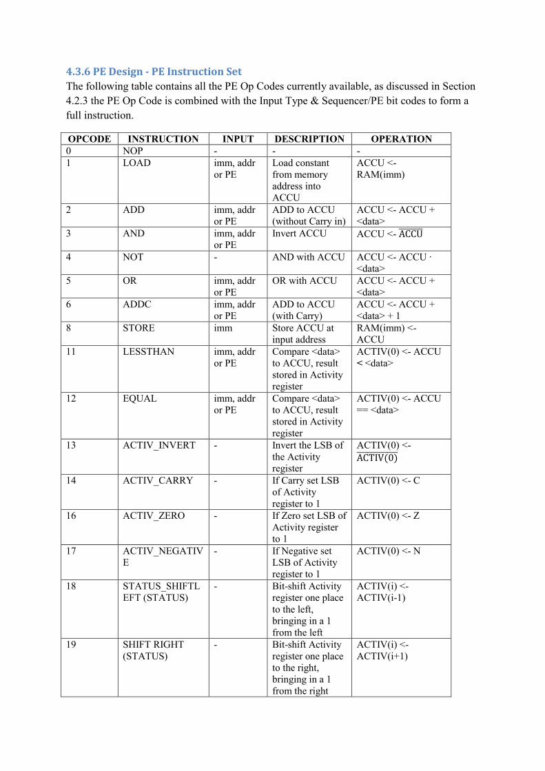
4.3.6 PE Design - PE Instruction Set The following table contains all the PE Op Codes currently available, as discussed in Section 4.2.3 the PE Op Code is combined with the Input Type & Sequencer/PE bit codes to form a full instruction.
OPCODE INSTRUCTION INPUT DESCRIPTION OPERATION 0 NOP - - - 1 LOAD imm, addr
or PE Load constant from memory address into ACCU
ACCU <- RAM(imm)
2 ADD imm, addr or PE
ADD to ACCU (without Carry in)
ACCU <- ACCU + <data>
3 AND imm, addr or PE
Invert ACCU ACCU <- ACCUതതതതതതത
4 NOT - AND with ACCU ACCU <- $&&8��<data>
5 OR imm, addr or PE
OR with ACCU ACCU <- ACCU + <data>
6 ADDC imm, addr or PE
ADD to ACCU (with Carry)
ACCU <- ACCU + <data> + 1
8 STORE imm Store ACCU at input address
RAM(imm) <- ACCU
11 LESSTHAN imm, addr or PE
Compare <data> to ACCU, result stored in Activity register
ACTIV(0) <- ACCU < <data>
12 EQUAL imm, addr or PE
Compare <data> to ACCU, result stored in Activity register
ACTIV(0) <- ACCU == <data>
13 ACTIV_INVERT - Invert the LSB of the Activity register
ACTIV(0) <- ACTIV(0)തതതതതതതതതതതത
14 ACTIV_CARRY - If Carry set LSB of Activity register to 1
ACTIV(0) <- C
16 ACTIV_ZERO - If Zero set LSB of Activity register to 1
ACTIV(0) <- Z
17 ACTIV_NEGATIVE
- If Negative set LSB of Activity register to 1
ACTIV(0) <- N
18 STATUS_SHIFTLEFT (STATUS)
- Bit-shift Activity register one place to the left, bringing in a 1 from the left
ACTIV(i) <- ACTIV(i-1)
19 SHIFT RIGHT (STATUS)
- Bit-shift Activity register one place to the right, bringing in a 1 from the right
ACTIV(i) <- ACTIV(i+1)

5. SIMD Image Processing This chapter will examine the application of the complete SIMD system design to a number
of various different routines useful in Image Processing. The Retro simulation results will be
provided, along with the expected results. The performance increase over a sequential (SISD)
system will also be examined for each routine.
A 5x5 PE grid will be used for all the following examples. For simplicity, the examples will
not cover the loading of data into each PE. All values shown on the PEs are in HEX. Note
that the value "--" is shown on a number of PEs, this is what Retro defines as an 'undefined'
value that comes from taking data from a wire which isn't driven by any source, in reality
these wires would simply be connected to ground and the value would be a '0'.

5.1 Summation Summation is important in a wide range of image processing routines, such as mean and sum
of absolute differences calculations[17]. Summation is a great example of the benefit of a
parallel system over a sequential system. Summing all 25 values in the following example on
a sequential system would take 25 separate ADD operations, that is MxN operations for a
MxN sized image. Compare this to the M+N-2 operations required using the designed SIMD
microprocessor, the difference is staggering for large amounts of data.
Figure 40 - Summation - Input
The above is the example input, with each PE having a value of 01. The values are summed
by first summing up each row and then summing the last column, which now contains the
row sums. The final output is held in the top-left PE, which can then be shifted into the
Sequencer CPU. The following is the complete instruction set required to complete the
summation:
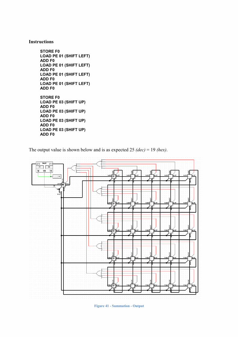
Instructions
STORE F0 LOAD PE 01 (SHIFT LEFT) ADD F0 LOAD PE 01 (SHIFT LEFT) ADD F0 LOAD PE 01 (SHIFT LEFT) ADD F0 LOAD PE 01 (SHIFT LEFT) ADD F0
STORE F0 LOAD PE 03 (SHIFT UP) ADD F0 LOAD PE 03 (SHIFT UP) ADD F0 LOAD PE 03 (SHIFT UP) ADD F0 LOAD PE 03 (SHIFT UP) ADD F0
The output value is shown below and is as expected 25 (dec) = 19 (hex).
Figure 41 - Summation - Output

5.2 Thresholding Thresholding is a simple example of using the PEs ability to compute IF statements.
Thresholding is used to convert greyscale images into binary images, based on a specific
threshold value. For this example, a threshold value of 80(hex) was used, this means all
values below 80 will be set to 00 and all above or equal to 80 will be set to FF.
Figure 42 - Thresholding - Input
Performing Thresholding on the designed PEs is very simple due to the inbuilt conditional
logic handling each PE has. The instructions are simply:
Instructions
LESSTHAN 80 LOAD 00 STATUS_INVERT LOAD FF

The output can be seen in below, as expected values less than 80 became 00 and values above
or equal to 80 became FF.
Figure 43 - Thresholding - Output
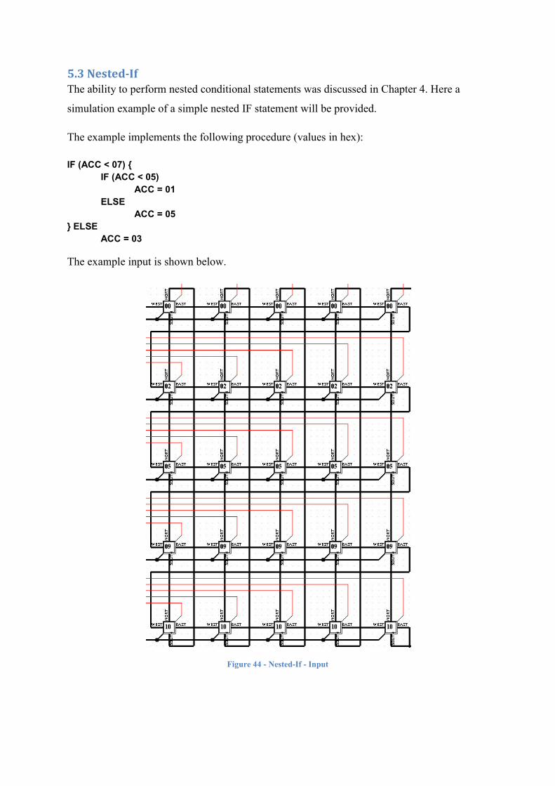
5.3 Nested-If The ability to perform nested conditional statements was discussed in Chapter 4. Here a
simulation example of a simple nested IF statement will be provided.
The example implements the following procedure (values in hex):
IF (ACC < 07) { IF (ACC < 05) ACC = 01 ELSE ACC = 05 } ELSE ACC = 03
The example input is shown below.
Figure 44 - Nested-If - Input
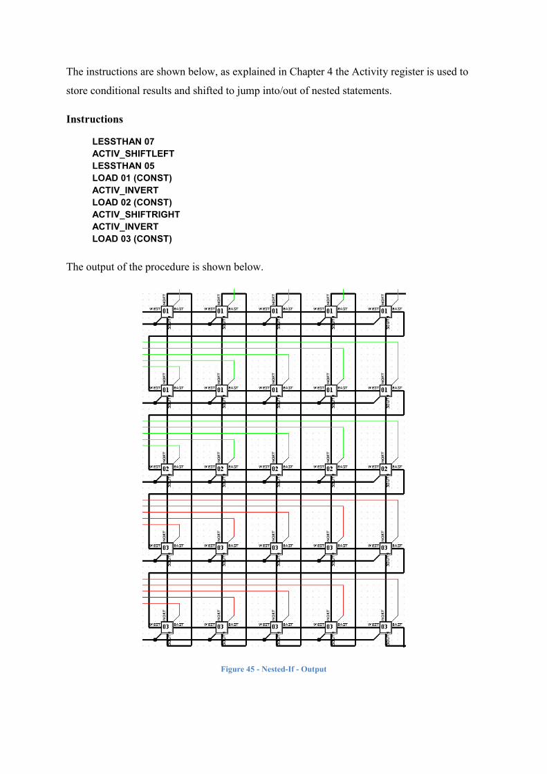
The instructions are shown below, as explained in Chapter 4 the Activity register is used to
store conditional results and shifted to jump into/out of nested statements.
Instructions
LESSTHAN 07 ACTIV_SHIFTLEFT LESSTHAN 05 LOAD 01 (CONST) ACTIV_INVERT LOAD 02 (CONST) ACTIV_SHIFTRIGHT ACTIV_INVERT LOAD 03 (CONST)
The output of the procedure is shown below.
Figure 45 - Nested-If - Output

5.4 While Loop Conditional looping was again discussed in Chapter 4, here a simple While loop was
implemented and simulated on the designed system. The procedure that was implemented
and the required instructions are below:
WHILE ( ACCU < 0F) { ACCU = ACUU + 1 }
Instructions
[00] LESSTHAN 0F [01] ADD 01 [02] BRR 00
Note that for Branch statements (BRR) it branches to the specified address, the address has
been shown to the left of each instruction. The Branch in this example simply goes back to
the LESSTHAN statement (address 00). The input for this example is shown below.
Figure 46 - While - Input

The output is shown below, as expected all the PEs values are now 0F except for the last row
whose values were already above 0F at the beginning.
Figure 47 - While - Output

5.5 Increase Image Brightness Increasing the brightness of an image is a very common image processing task. This is
usually done by a simple addition, there is however the issue of overflow if a value goes
above the maximum value. In digital logic, overflow has to be detected and acted upon as it
will usually not cause any errors so it can easily go undetected. This is done by having the
Overflow flag in the Status Register of each PE as discussed in Chapter 4.
In this example, the current Accumulator value will be doubled and if Overflow occurs the
Accumulator will be set to FF. Take note that all values are in HEX again. The instructions
required are:
Instructions
STORE F0 ADD F0 (ADDR) STATUS_CARRY LOAD FF (CONST)
The input for example shown below:
Figure 48 - Image Brightness - Input

To double the ACCU value the current value is first stored and then added to the current
value. The Overflow flag is then checked, disabling any PEs which had no overflow from the
previous addition and enabling any that did. The LOAD FF is then carried out on all active
PEs (those which had Overflow). The result and image representation are shown below:
Figure 49 - Image Brightness - Output
Input Image Output Image

5.6 Sobel Edge Detection The previous examples show the basic functionality of the SIMD system and some basic
image processing applications. This example looks at a complex image processing routine -
Sobel Edge Detection. Sobel edge detection is used to find edges in an image by using the
Sobel operator [18]. The Sobel operator is the following matrices:
-1 0 1 1 2 1
-2 0 2 0 0 0
-1 0 1 -1 -2 -1 Gx Gy
The first matrix is for detecting vertical edges and the second is for detecting horizontal
edges. The combination of the results of applying these matrices then gives the final Sobel
values using the following equation.
|ܩ| = ටܩ௫ଶ + ௬ଶܩ
The above equation is hard to compute in discrete logic so the following approximation is used:
|ܩ| = ௫ܩ| | + ௬ܩ| |
The matrices are applied by positioning the middle element (highlighted in red above) at the
current pixel and then multiplying the surrounding pixels by the values in the matrices and
finally summing all those values together to give the Sobel value at that pixel.
The parallelisation of the SIMD system and the PE grid shine in this example. 25 Sobel
operations can be carried out in parallel in a 5x5 PE grid, which greatly increases
performance. This is made possible by having the PEs connected in a NEWS grid as
discussed in Chapter 4. The grid matches the matrices so we can simply shift and store each
neighbouring value and then add the required multiples of each neighbour. This means for
any number of PE elements the number of instructions required to apply the Sobel operators
is exactly the same. The required instructions are shown on the next page.
The majority of the instructions have already been explained. Of note is the use of the
STATUS_NEGATIVE operation to check if the Negative flag is set, if it is the magnitude of
each PE with a negative value is computed by inverting the current bits and then
incrementing the result by one.

Instructions
STORE ff SHIFT UP STORE c1 SHIFT LEFT STORE c2 LOAD ff SHIFT UP SHIFT RIGHT STORE c0 LOAD ff SHIFT DOWN STORE a1 SHIFT LEFT STORE a2 LOAD ff SHIFT DOWN SHIFT RIGHT STORE a0 LOAD ff SHIFT LEFT STORE b2 LOAD ff SHIFT RIGHT STORE b0 LOAD 00 (CNST) ADD c0 ADD c1 ADD c1 ADD c2 STORE 10 LOAD 00 (CNST) ADD a0 ADD a1 ADD a1 ADD a2 INVERT ADD_WITHCARRY ADDR 10 STATUS_NEGATIVE
INVERT ADD 01 (CNST) ACTIV_SHIFTRIGHT STORE F0 LOAD 00 (CNST) ADD a0 ADD b0 ADD b0 ADD c0 STORE 20 LOAD 00 (CNST) ADD a2 ADD b2 ADD b2 ADD c2 INVERT ADD_WITHCARRY ADDR 10 STATUS_NEGATIVE INVERT ADD 01 (CNST) ACTIV_SHIFTRIGHT STORE f1 ADD f0 (ADDR)

The input for the Sobel operation is shown below.
Figure 50 - Sobel - Input
These input values represent the following image.
Input Image

The output after the Sobel operation is shown below.
Figure 51 - Sobel - Output
The Sobel operator works better on larger images where the boundaries have much less effect on the output image. The outer edge of pixels after the application of the Sobel operator is usually discarded as the boundary produces values that are not useful. The image representation of the above output values is shown below.
Output Image

6. VHDL Simulation Once the Retro simulations were completed and the design finalised the VHDL generation
began. This included the time consuming job of implementing all the Retro components in
VHDL and allowing the Java code that generated the VHDL to handle each component and
its respective properties as explained in Section 3.3.3. Due to this, the full SIMD system was
unable to have its VHDL simulated. However the VHDL generated for each PE has been
checked and simulated successfully.
6.1 PE Simulation To simulate the VHDL, the free version of Vivado Design Suite by Xilinx was used [19].
Vivado Design Suite is a very powerful tool for digital system design, for this project it was
used only for the behavioural simulation of the VHDL generated from Retro.
It is difficult to fully show the functionality of the VHDL as the simulation is now a lower
level, looking at each signal rather than the high level graphical overview Retro produced.
However the following examples show the major features of the PEs were simulating
successfully using the generated VHDL. The full VHDL generated for the PE can be seen in
Appendix 3.0.

6.1.1 Addition The following example shows a simple incremental addition. The operand is set to 01
(CONSTANT) and the PE Op Code for addition (02) is given. The simulation results are
shown below.
Figure 52 - VHDL Simulation - Addition
The above waveforms show the addition of 01 to the Accumulator value each time the clock
(signal 'clk') pulses. The clock begins at 100ns and from there ACCU value can be seen to
increase by 1 each clock cycle. The input operand and Op Code can also be seen on the above
waveform view.
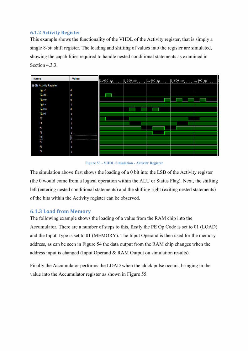
6.1.2 Activity Register This example shows the functionality of the VHDL of the Activity register, that is simply a
single 8-bit shift register. The loading and shifting of values into the register are simulated,
showing the capabilities required to handle nested conditional statements as examined in
Section 4.3.3.
Figure 53 - VHDL Simulation - Activity Register
The simulation above first shows the loading of a 0 bit into the LSB of the Activity register
(the 0 would come from a logical operation within the ALU or Status Flag). Next, the shifting
left (entering nested conditional statements) and the shifting right (exiting nested statements)
of the bits within the Activity register can be observed.
6.1.3 Load from Memory The following example shows the loading of a value from the RAM chip into the
Accumulator. There are a number of steps to this, firstly the PE Op Code is set to 01 (LOAD)
and the Input Type is set to 01 (MEMORY). The Input Operand is then used for the memory
address, as can be seen in Figure 54 the data output from the RAM chip changes when the
address input is changed (Input Operand & RAM Output on simulation results).
Finally the Accumulator performs the LOAD when the clock pulse occurs, bringing in the
value into the Accumulator register as shown in Figure 55.

Figure 54 - VHDL Simulation - Load (RAM)
Figure 55 - VHDL Simulation - Load (ACCU)

7. Conclusion This project had two focuses; the SIMD system design and further developing Retro for
modular design, and VHDL generation. The design was ultimately successful with the
potential performance and functionality of the final system exhibited from Retro simulations.
The simulations proved that there is still a place for SIMD architecture devices in specialised
parallel processing applications, specifically multimedia processing.
The Retro extensions and debugging was a major part of this project. The main extensions
were adding the ability to modularise designs (allowing the simulation of the SIMD system)
and the addition of automatic VHDL generation. Throughout the development of Retro,
numerous bug fixes and small user interface changes were made. The VHDL generation was
a substantial project in of itself, having to account for a wide variety of components and their
respective properties within Retro. Due to this, the VHDL generation was focussed on getting
the VHDL behavioural simulation to mirror the functionality of the circuit as it was in Retro.
Apart from a few minor logic components, the VHDL generation development is now
complete.
The SIMD system was designed from the ground up, with the Sequencer CPU and PEs both
being designed with image processing in mind. The system was created in Retro and
simulations of various image processing were implemented on the system to assess its
performance and functionality. The simulations showed that the design has vast performance
increases over a sequential processing unit and PE design enabled a different approach to
handling conditional procedures in an SIMD system.
The SIMD design included a number of features not seen usually seen in SIMD image
processing devices. The main additional feature was the ability for each PE to handle nested
conditional statements and loops. The basis of both these functions was the addition of an
Activity register in the PE design. The ability to handle conditional looping and nested
conditional statements allows better performance and simpler programming of a number of
image processing routines.
7.1 Future Work Due to the time taken to implement VHDL generation within Retro, the VHDL of the
complete SIMD system was unable to be tested. The final step in this project is simulating the
VHDL and then putting it onto an FPGA for physical testing.
There is still also some work to be done on the VHDL generation in Retro as some
components that were not used in the SIMD design were omitted from the VHDL generation
due to the time required to implement each component. The VHDL generation code was done
through a single method for each component so adding the extra generation code is not overly
complex, simply more time consuming than this project allowed. Additional features that
could further improve the VHDL generation, is firstly using a naming convention for the
wires (currently each wire is simply called 'temp(id)' where id is the wire's unique ID). The
register and RAM components could also use the label set in Retro as the component name in
the VHDL to further improve usability of the VHDL, this could also be done for the other
components although the majority of components do not have labels that could be used so
another naming convention would have to be employed.
Retro itself is still based on the old Java AWT framework which has been deprecated in
newer versions of Java. There are therefore a number of issues with Retro still using the
AWT framework. In this project, a number of workarounds were implemented to allow the
use of Retro with Java 7. However redesigning Retro using the Java Swing framework would
be very beneficial to the continued use of Retro for teaching at UWA.
References
[1] C. Ozdogan. (2010, 15/04/2014). Flynn's Taxonomy. Available: http://siber.cankaya.edu.tr/ParallelComputing/ceng471/node14.html
[2] W. J. Bouknight, S. A. Denenberg, D. E. McIntyre, J. M. Randall, A. H. Sameh, and D. L. Slotnick, "The Illiac IV system," Proceedings of the IEEE, vol. 60, pp. 369-388, 1972.
[3] H. Falk, "What went wrong V: Reaching for a gigaflop: The fate of the famed Illiac IV was shaped by both research brilliance and real-world disasters," Spectrum, IEEE, vol. 13, pp. 65-70, 1976.
[4] W. D. Hillis, The Connection Machine: Cambridge, 1989. [5] I. Corporation, "PENTIUM® PROCESSOR WITH MMX™ TECHNOLOGY," I.
Corporation, Ed., ed. Mt. Prospec: Intel Corporation, 1997. [6] A. T.J., N. G.R., F. N.D., K. D.J., P. R.A., and V. G.J.B, "A Scalable Multiple-SIMD
Architecture for Real-Time Image Understanding," 1990. [7] T. Kurafuji, M. Haraguchi, M. Nakajima, T. Nishijima, T. Tanizaki, H. Yamasaki, et
al., "A Scalable Massively Parallel Processor for Real-Time Image Processing," IEEE Journal of Solid-State Circuits, vol. 46, 2011.
[8] O. R. e. al, "Highly Parallel Image Processing on a Massively Parallel Processor Array," 2009.
[9] B. Svensson, "SIMD Architectures," 1992. [10] R. M. Hord, Parallel Supercomputing in SIMD Architectures, 1990. [11] O. Corporation. (2011, 19 Jul 2013). Abstract Window Toolkit (AWT). Available:
http://docs.oracle.com/javase/6/docs/technotes/guides/awt/ [12] M. Bunge, "A General Black Box Theory," Philosophy of Science, vol. 30, pp. 346-
358, 1963. [13] M. Sung, "SIMD Parallel Processing," Massachusetts Institute of Technology,
Cambridge2000. [14] T. Bräunl. (2014). Retro Example: CPU 4. Available:
http://robotics.ee.uwa.edu.au/retro/examples/cpu4.html [15] R. Fisher, S. Perkins, A. Walker, and E. Wolfart. (2003, 21/05/2014). Morphology -
Thinning. Available: http://homepages.inf.ed.ac.uk/rbf/HIPR2/thin.htm [16] R. Lerman, D. S. Raicu, and J. D. Furst, "Contrast enhancement of soft tissues in
Computed Tomography images," School of Computer Science, Telecommunications, and Information Systems, DePaul University, Chicago, IL 60604, USA, 2006.
[17] J. Olivares, J. Hormigo, J. Villalba, and I. Benavides, "Minimum Sum of Absolute Differences implementation in a single FPGA device," Dept. of Electrotechnics and Electronics, University of C¶ordoba, 2004.
[18] R. Fisher, S. Perkins, A. Walker, and E. Wolfart. (2003, 24/05/2014). Feature Detectors - Sobel Operator. Available: http://homepages.inf.ed.ac.uk/rbf/HIPR2/sobel.htm
[19] Xilinx. (2014, 10/12/2013). Vivado Design Suite Evaluation and WEBPACK. Available: http://www.xilinx.com/products/design_tools/vivado/vivado-webpack.htm

Appendices
Appendix 1.0 - SimulationEngine Class Excerpt public class SimulationEngine { private EnginePeerList components; // list of all components private NodeList nodes; // list of data at each node private double currentTime; private EnginePeerList currentAffected; private NodeList mostRecent; private EnginePeerList displaymods; public SimulationEngine(EnginePeerList gates, NodeList connection) { this.components = gates; this.displaymods = new EnginePeerList(); for (int k = 0; k < gates.getSize(); k++) { if(gates.getItemAt(k).getParent() instanceof sim.lib.others.Module) this.displaymods.insertDistinctItem(gates.getItemAt(k)); } this.nodes = connection; this.currentTime = 0; this.currentAffected = new EnginePeerList(); this.mostRecent = new NodeList(); }
}
Appendix 1.1 - Module Drawing public void paint(Graphics g) { // draw if visible if (this.isVisible()) { int gridGap = CentralPanel.ACTIVE_GRID.getCurrentGridGap(); int increment = gridGap / 4; int offset = 2 * gridGap; g.setColor(Color.WHITE); g.fillRect(2 * gridGap + increment / 2, 2 * gridGap + increment / 2, offset - increment, offset - increment); g.setColor(this.brush); g.drawRect(2 * gridGap, 2 * gridGap, offset, offset); g.drawRect(2 * gridGap + increment / 2, 2 * gridGap + increment / 2, offset - increment, offset - increment); int start = 3 * gridGap; int end = 5 * gridGap; offset = 2 * gridGap; g.setFont(new Font(Wrapper.FONT_NAME, Font.BOLD, gridGap * 2 / 3)); Font f = new Font(Wrapper.FONT_NAME, Font.PLAIN, 3 * increment); String name; if (modLabel == null) { String parts[] = this.modpath.split("\\\\");

name = parts[parts.length - 1]; name = name.substring(0, name.length() - 4); this.modLabel = name; } else { name = modLabel; } int col = 0; if (this.regOut != null) { if (this.regOut instanceof sim.lib.memory.Register) { name = ((sim.lib.memory.Register)this.regOut).getValue(); col = Integer.decode("0x" + name); }else if (this.regOut instanceof sim.lib.memory.ShiftRegister) { name = ((sim.lib.memory.ShiftRegister)this.regOut).getValue(); col = Integer.decode("0x" + name); } if (this.colour) { g.setColor(new Color(col,col,col)); g.fillRect(2 * gridGap + increment / 2, 2 * gridGap + increment / 2, offset-increment, offset-increment); name = ""; g.setColor(Color.BLACK); }else{ g.setFont(new Font(Wrapper.FONT_NAME, Font.BOLD, gridGap)); } } g.drawString(name, 2 * gridGap + increment + 1, gridGap * 2 + 5 * increment); offset = offset + gridGap; //**********Draw ports based on number of pins in input file********** g.setFont(new Font(Wrapper.FONT_NAME, Font.PLAIN, gridGap * 2 / 3)); if(this.pin99){ g.drawLine(4 *gridGap, 2 * gridGap, 5 * gridGap, 1 * gridGap); //portF (DIAGONAL) } if (this.numPin > 0) { g.drawString(this.labels[0].substring(0, Math.min(5, this.labels[0].length())), gridGap / 8, gridGap * 5 / 2 + increment); //GET PIN NAMES FROM INPUT FILE g.fillRect(0, 3 * gridGap - 1, 2 * gridGap, 3); //portA (LEFT) } if (this.numPin > 1) { AffineTransform tmp = f.getTransform(); AffineTransform at = new AffineTransform(); at.rotate(-90 * java.lang.Math.PI / 180); Font tf = f.deriveFont(at); g.setFont(tf.deriveFont((float) (gridGap * 2 / 3))); g.drawString(this.labels[1].substring(0, Math.min(5, this.labels[1].length())), gridGap * 11 / 4, gridGap * 2 - gridGap / 8);

g.fillRect(3 * gridGap - 1, 0, 3, 2 * gridGap); //portB (TOP) } if (this.numPin > 2) { g.setFont(new Font(Wrapper.FONT_NAME, Font.PLAIN, gridGap * 2 / 3)); g.drawString(this.labels[2].substring(0, Math.min(5, this.labels[2].length())), gridGap * 4 + gridGap / 8, gridGap * 5 / 2 + increment); g.fillRect(4 * gridGap, 3 * gridGap - 1, 2 * gridGap, 3); //portC (RIGHT) } if (this.numPin > 3) { AffineTransform tmp = f.getTransform(); AffineTransform at = new AffineTransform(); at.rotate(-90 * java.lang.Math.PI / 180); Font tf = f.deriveFont(at); g.setFont(tf.deriveFont((float) (gridGap * 2 / 3))); g.drawString(this.labels[3].substring(0, Math.min(5, this.labels[3].length())), gridGap * 7 / 2 + gridGap / 8, gridGap * 6 - gridGap / 8); g.fillRect(3 * gridGap - 1, 4 * gridGap, 3, 2 * gridGap); //portD (BOTTOM) } if (this.numPin > 4) { g.drawLine(gridGap, 5 * gridGap, 2 * gridGap, 4 * gridGap); //portE (DIAGONAL) g.drawLine(gridGap, 5 * gridGap - 1, 2 * gridGap, 4 * gridGap - 1); //portE (DIAGONAL) g.drawLine(gridGap, 5 * gridGap + 1, 2 * gridGap, 4 * gridGap + 1); //portE (DIAGONAL) } } }
Appendix 1.2 - Module Setup & Loading Setup
public void setPath(String file) { this.modpath = file; //LOAD numPin = number of pin components from file //get names for pins into string array this.numPin = 0; Grid g = new Grid(); String[] basics, specifics; String className, componentName, readIn; BufferedReader inStream; Wrapper created; int z = 0; try { inStream = new BufferedReader(new FileReader(file)); readIn = SaveLoadShortcut.GUI_FILE_LINK.extractParameter(inStream);
SaveLoadShortcut.GUI_FILE_LINK.readBlank(inStream); SaveLoadShortcut.GUI_FILE_LINK.extractParameters(g.getNumberOfParameters(), inStream); SaveLoadShortcut.GUI_FILE_LINK.readBlank(inStream); int size = Integer.valueOf(SaveLoadShortcut.GUI_FILE_LINK.extractParameter(inStream)).intValue(); for (int index = 0; index < size; index++) { SaveLoadShortcut.GUI_FILE_LINK.readBlank(inStream); className = SaveLoadShortcut.GUI_FILE_LINK.extractParameter(inStream); componentName = SaveLoadShortcut.GUI_FILE_LINK.extractParameter(inStream); created = SaveLoadShortcut.GUI_FILE_LINK.getWrapper(className); basics = SaveLoadShortcut.GUI_FILE_LINK.extractParameters(created.getNumberOfBasicParameters(), inStream); specifics = SaveLoadShortcut.GUI_FILE_LINK.extractParameters(created.getNumberOfSpecificParameters(), inStream); if (className.equals("sim.lib.outputs.Pin")) { if(Integer.valueOf(specifics[1]) == 99) this.pin99 = true; else this.numPin++; this.busSizes[Integer.valueOf(specifics[1]) - 1] = Integer.valueOf(specifics[0]); //get bus size for each pin this.labels[Integer.valueOf(specifics[1]) - 1] = specifics[2]; //get label string for each pin } else if (className.equals("sim.lib.memory.Register") || className.equals("sim.lib.memory.ShiftRegister")) { this.regList[z] = specifics[2]; z++; } } lastPath = file; } catch (Exception e) { if (!loadError) { JOptionPane.showMessageDialog(null, "Error loading module file, please correct file paths in Control Center", "ERROR", JOptionPane.ERROR_MESSAGE); loadError = true; } } }

Loading
private Object[] loadModule(String fname) { String inFile = fname; Reader inStream; MainWindow.CENTRAL_PANEL.createGrid(""); CentralPanel.ACTIVE_GRID = new Grid(); try { MainWindow.CENTRAL_PANEL.createGrid("MODULE"); MainWindow.CENTRAL_PANEL.setVisible(false); inStream = new BufferedReader(new FileReader(inFile)); SaveLoadShortcut.GUI_FILE_LINK.loadMod(inStream, CentralPanel.ACTIVE_GRID); inStream.close(); } catch (FileNotFoundException e) { // TODO Auto-generated catch block e.printStackTrace(); } catch (SimException e) { // TODO Auto-generated catch block e.printStackTrace(); } catch (IOException e) { e.printStackTrace(); } //Get EnginePeers from file //insert into input EnginePeerList //connect relevant nodes Grid g = CentralPanel.ACTIVE_GRID; //*******LOAD COMPONENTS FROM FILE****** int loop; int wires = g.getNumberOfWires(); int junctions = g.getNumberOfJunctions(); int splitters = g.getNumberOfSplitters(); int components = g.getNumberOfComponents(); int total; NodeList tempnl = new NodeList(); EnginePeerList tempepl = new EnginePeerList(); for (loop = 0; loop < junctions; loop++) { ((NodeModule) g.getComponent(loop)).createNode(tempnl); } total = junctions + wires + splitters; for (loop = junctions + wires; loop < total; loop++) { ((SplitterModule) g.getComponent(loop)).mergeNodes(tempnl); } total = total + components; for (loop = junctions + wires + splitters; loop < total; loop++) { ((EngineModule) g.getComponent(loop)).createEnginePeer(tempepl); }
Object[] out = new Object[2]; out[0] = tempepl; out[1] = tempnl; return out; } public void createEnginePeer(EnginePeerList epl, NodeList nl) { //ENGINE PEER FOR MODULE this.busSize = 8; Object[] tmp = loadModule(this.modpath); //load EPL and NL from file EnginePeerList tempepl = (EnginePeerList) tmp[0]; NodeList tempnl = (NodeList) tmp[1]; int[] pinpos = new int[this.busSizes.length]; //array to hold current bit position of each pin for (Object o : tempepl) { EnginePeer ept = (EnginePeer) o; if (!ept.getParent().getClass().toString().equals("class sim.lib.outputs.Pin")) { for (int k = 0; k < ept.getInputPins().getSize(); k++) { for (int i = 0; i < ept.getInputPins().getItemAt(k).getConnection().getSize(); i++) { EnginePeer eptt = ept.getInputPins().getItemAt(k).getConnection().getItemAt(i); if (eptt.getParent().getClass().toString().equals("class sim.lib.outputs.Pin")) { //component connected to a pin int n = ((sim.lib.outputs.Pin) eptt.getParent()).getNumber(); if(pinpos[n-1] >= eptt.getInputPins().size()){ pinpos[n-1] = 0; } if (!ept.getInputPins().getItemAt(k).equals(eptt.getInputPins().getItemAt(pinpos[n - 1]))) { //find correct bit position of pin pinpos[n - 1] = 0; while (!ept.getInputPins().getItemAt(k).equals(eptt.getInputPins().getItemAt(pinpos[n - 1]))) { pinpos[n - 1]++; } } switch (n) //connect pins from loaded file to ports on module component { case 1: ept.setInputPin(k, this.portA.getNodes().getItemAt(pinpos[n - 1])); pinpos[n - 1]++; break; case 2: ept.setInputPin(k, this.portB.getNodes().getItemAt(pinpos[n - 1]));

pinpos[n - 1]++; break; case 3: ept.setInputPin(k, this.portC.getNodes().getItemAt(pinpos[n - 1])); pinpos[n - 1]++; break; case 4: ept.setInputPin(k, this.portD.getNodes().getItemAt(pinpos[n - 1])); pinpos[n - 1]++; break; case 99: ept.setInputPin(k, this.portF.getNodes().getItemAt(pinpos[n - 1])); pinpos[n - 1]++; break; default: int base = 0; //n = n - 1; for (int j = 4; j <= (n - 2); j++) { //get correct starting bit position for portE base = base + this.busSizes[j]; } int a = base + pinpos[n - 1]; System.out.println(k + "," + a); ept.setInputPin(k, this.portE.getNodes().getItemAt(base + pinpos[n - 1])); pinpos[n - 1]++; } break; } } } Arrays.fill(pinpos, 0); //reset array to hold current bit position of each pin if (ept.getOutputPins() != null) { for (int k = 0; k < ept.getOutputPins().getSize(); k++) { for (int i = 0; i < ept.getOutputPins().getItemAt(k).getConnection().getSize(); i++) { EnginePeer eptt = ept.getOutputPins().getItemAt(k).getConnection().getItemAt(i); if (eptt.getParent().getClass().toString().equals("class sim.lib.outputs.Pin")) { int n = ((sim.lib.outputs.Pin) eptt.getParent()).getNumber(); if(pinpos[n-1] >= eptt.getInputPins().getSize()){ pinpos[n-1] = 0; } if (!ept.getOutputPins().getItemAt(k).equals(eptt.getInputPins().getItemAt(pinpos[n - 1]))) { //find correct bit position of pin

pinpos[n - 1] = 0; while (!ept.getOutputPins().getItemAt(k).equals(eptt.getInputPins().getItemAt(pinpos[n - 1]))) { pinpos[n - 1]++; } } switch (n) { case 1: ept.setOutputPin(k, this.portA.getNodes().getItemAt(pinpos[n - 1])); pinpos[n - 1]++; break; case 2: ept.setOutputPin(k, this.portB.getNodes().getItemAt(pinpos[n - 1])); pinpos[n - 1]++; break; case 3: ept.setOutputPin(k, this.portC.getNodes().getItemAt(pinpos[n - 1])); pinpos[n - 1]++; break; case 4: ept.setOutputPin(k, this.portD.getNodes().getItemAt(pinpos[n - 1])); pinpos[n - 1]++; break; case 99: ept.setOutputPin(k, this.portF.getNodes().getItemAt(pinpos[n - 1])); pinpos[n - 1]++; break; default: int base = 0; for (int j = 4; j <= (n - 2); j++) { //get correct starting bit position for portE base = base + this.busSizes[j]; } ept.setOutputPin(k, this.portE.getNodes().getItemAt(base + pinpos[n - 1])); pinpos[n - 1]++; } break; } } } } epl.insertItem(ept); if (ept.getParent() instanceof sim.lib.memory.Register) { if (((sim.lib.memory.Register) ept.getParent()).getRegName().equals(this.regName)) {

this.regOut = ((sim.lib.memory.Register) ept.getParent()); } } if (ept.getParent() instanceof sim.lib.memory.ShiftRegister) { if (((sim.lib.memory.ShiftRegister) ept.getParent()).getRegName().equals(this.regName)) { this.regOut = ((sim.lib.memory.ShiftRegister) ept.getParent()); } } } } EnginePeer ep = new EnginePeer(0, 0, this); epl.insertItem(ep); for (Object n : tempnl) { for (Object w : ((Node) n).getWires()) { ((Wire) w).setVisible(false); } EnginePeerList epltemp = ((Node) n).getConnection(); for (Object c : epltemp) { ((EnginePeer) c).getParent().getParentWrapper().setVisible(false); } nl.insertItem((Node) n); } }
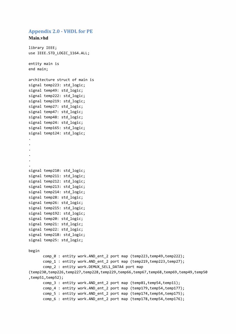
Appendix 2.0 - VHDL for PE Main.vhd
library IEEE;
use IEEE.STD_LOGIC_1164.ALL;
entity main is
end main;
architecture struct of main is
signal temp223: std_logic;
signal temp49: std_logic;
signal temp222: std_logic;
signal temp219: std_logic;
signal temp27: std_logic;
signal temp47: std_logic;
signal temp48: std_logic;
signal temp24: std_logic;
signal temp165: std_logic;
signal temp124: std_logic;
.
.
.
.
.
.
signal temp210: std_logic;
signal temp211: std_logic;
signal temp212: std_logic;
signal temp213: std_logic;
signal temp214: std_logic;
signal temp28: std_logic;
signal temp26: std_logic;
signal temp215: std_logic;
signal temp192: std_logic;
signal temp20: std_logic;
signal temp21: std_logic;
signal temp22: std_logic;
signal temp218: std_logic;
signal temp25: std_logic;
begin
comp_0 : entity work.AND_ent_2 port map (temp223,temp49,temp222);
comp_1 : entity work.AND_ent_2 port map (temp219,temp223,temp27);
comp_2 : entity work.DEMUX_SEL1_DATA4 port map
(temp230,temp226,temp227,temp228,temp229,temp66,temp67,temp68,temp69,temp49,temp50
,temp51,temp52);
comp_3 : entity work.AND_ent_2 port map (temp81,temp54,temp11);
comp_4 : entity work.AND_ent_2 port map (temp179,temp54,temp177);
comp_5 : entity work.AND_ent_2 port map (temp174,temp54,temp175);
comp_6 : entity work.AND_ent_2 port map (temp178,temp54,temp176);

comp_7 : entity work.REGISTER_8 port map
(temp72,temp73,temp74,temp75,temp76,temp77,temp78,temp79,temp217,temp41,temp42,tem
p43,temp44,temp45,temp46,temp47,temp48);
comp_8 : entity work.NOT_ent port map (temp24,temp165);
comp_9 : entity work.TRISTATE_8 port map
(temp12,temp13,temp14,temp15,temp16,temp17,temp18,temp19,temp165,temp166,temp167,t
emp168,temp169,temp170,temp171,temp172,temp173);
comp_10 : entity work.RAM_ADDR256_DATA8 port map
(temp92,temp92,temp24,temp56,temp57,temp58,temp59,temp60,temp61,temp62,temp63,temp
166,temp167,temp168,temp169,temp170,temp171,temp172,temp173);
comp_11 : entity work.MUX_SEL3_DATA8 port map
(temp66,temp67,temp68,temp12,temp13,temp14,temp15,temp16,temp17,temp18,temp19,temp
84,temp85,temp86,temp87,temp88,temp89,temp90,temp91,temp93,temp94,temp95,temp96,te
mp97,temp98,temp99,temp100,temp101,temp102,temp103,temp104,temp105,temp106,temp107
,temp108,temp109,temp110,temp111,temp112,temp113,temp114,temp115,temp116,temp117,t
emp118,temp119,temp120,temp121,temp122,temp123,temp124,temp93,temp94,temp95,temp96
,temp97,temp98,temp99,temp100,temp2,temp3,temp4,temp5,temp6,temp7,temp8,temp9,temp
183,temp184,temp185,temp186,temp187,temp188,temp189,temp75);
comp_12 : entity work.REGISTER_8 port map
(temp183,temp184,temp185,temp186,temp187,temp188,temp189,temp75,temp10,temp12,temp
13,temp14,temp15,temp16,temp17,temp18,temp19);
comp_13 : entity work.EQUALTObus_ent_5_8 port map
(temp226,temp227,temp228,temp229,temp230,temp216);
comp_14 : entity work.CONSTANT_0 port map (temp92);
comp_15 : entity work.ANDbus_ent_8 port map
(temp12,temp13,temp14,temp15,temp16,temp17,temp18,temp19,temp84,temp85,temp86,temp
87,temp88,temp89,temp90,temp91,temp101,temp102,temp103,temp104,temp105,temp106,tem
p107,temp108);
comp_16 : entity work.COMPLEMENTbus_ent_8 port map
(temp12,temp13,temp14,temp15,temp16,temp17,temp18,temp19,temp109,temp110,temp111,t
emp112,temp113,temp114,temp115,temp116);
comp_17 : entity work.LESSbus_ent_8 port map
(temp12,temp13,temp14,temp15,temp16,temp17,temp18,temp19,temp84,temp85,temp86,temp
87,temp88,temp89,temp90,temp91,temp191);
comp_18 : entity work.EQUALbus_ent_8 port map
(temp12,temp13,temp14,temp15,temp16,temp17,temp18,temp19,temp84,temp85,temp86,temp
87,temp88,temp89,temp90,temp91,temp65);
comp_19 : entity work.AND_ent_2 port map (temp71,temp217,temp10);
comp_20 : entity work.ORbus_ent_8 port map
(temp12,temp13,temp14,temp15,temp16,temp17,temp18,temp19,temp84,temp85,temp86,temp
87,temp88,temp89,temp90,temp91,temp117,temp118,temp119,temp120,temp121,temp122,tem
p123,temp124);
comp_21 : entity work.TRISTATE_8 port map
(temp12,temp13,temp14,temp15,temp16,temp17,temp18,temp19,temp11,temp133,temp134,te
mp135,temp136,temp137,temp138,temp139,temp140);
comp_22 : entity work.TRISTATE_8 port map
(temp12,temp13,temp14,temp15,temp16,temp17,temp18,temp19,temp175,temp141,temp142,t
emp143,temp144,temp145,temp146,temp147,temp148);
comp_23 : entity work.TRISTATE_8 port map
(temp12,temp13,temp14,temp15,temp16,temp17,temp18,temp19,temp176,temp149,temp150,t
emp151,temp152,temp153,temp154,temp155,temp156);

comp_24 : entity work.TRISTATE_8 port map
(temp12,temp13,temp14,temp15,temp16,temp17,temp18,temp19,temp177,temp157,temp158,t
emp159,temp160,temp161,temp162,temp163,temp164);
comp_25 : entity work.MUX_SEL2_DATA8 port map
(temp56,temp57,temp141,temp142,temp143,temp144,temp145,temp146,temp147,temp148,tem
p133,temp134,temp135,temp136,temp137,temp138,temp139,temp140,temp157,temp158,temp1
59,temp160,temp161,temp162,temp163,temp164,temp149,temp150,temp151,temp152,temp153
,temp154,temp155,temp156,temp125,temp126,temp127,temp128,temp129,temp130,temp131,t
emp132);
comp_26 : entity work.MUX_SEL2_DATA8 port map
(temp53,temp54,temp56,temp57,temp58,temp59,temp60,temp61,temp62,temp63,temp166,tem
p167,temp168,temp169,temp170,temp171,temp172,temp173,temp125,temp126,temp127,temp1
28,temp129,temp130,temp131,temp132,temp125,temp126,temp127,temp128,temp129,temp130
,temp131,temp132,temp84,temp85,temp86,temp87,temp88,temp89,temp90,temp91);
comp_27 : entity work.DECODER_2 port map
(temp56,temp57,temp81,temp174,temp178,temp179);
comp_28 : entity work.SHIFTREGISTER_8 port map
(temp207,temp208,temp209,temp210,temp211,temp212,temp213,temp214,temp217,temp28,te
mp26,temp215,temp26,temp192,temp208,temp209,temp210,temp211,temp212,temp213,temp21
4,temp20,temp21);
comp_29 : entity work.MUX_SEL3_DATA1 port map
(temp49,temp50,temp51,temp192,temp191,temp65,temp22,temp41,temp42,temp43,temp44,te
mp207);
comp_30 : entity work.NOT_ent port map (temp192,temp22);
comp_31 : entity work.AND_ent_2 port map (temp216,temp71,temp218);
comp_32 : entity work.NAND_ent_2 port map (temp218,temp25,temp24);
comp_33 : entity work.ADDbus_ent_8 port map
(temp12,temp13,temp14,temp15,temp16,temp17,temp18,temp19,temp84,temp85,temp86,temp
87,temp88,temp89,temp90,temp91,temp68,temp93,temp94,temp95,temp96,temp97,temp98,te
mp99,temp100,temp72);
comp_34 : entity work.CONSTANT_1 port map (temp26);
comp_35 : entity work.AND_ent_2 port map (temp52,temp27,temp215);
comp_36 : entity work.EQUALTObus_ent_8_255 port map
(temp192,temp208,temp209,temp210,temp211,temp212,temp213,temp214,temp71);
comp_37 : entity work.NOT_ent port map (temp49,temp219);
comp_38 : entity work.AND_ent_2 port map (temp52,temp222,temp28);
comp_39 : entity work.EQUALTObus_ent_8_0 port map
(temp12,temp13,temp14,temp15,temp16,temp17,temp18,temp19,temp74);
end struct;

Gates.vhd
library IEEE;
use IEEE.STD_LOGIC_1164.ALL;
entity AND_ent_2 is
port( x0: in std_logic;
x1: in std_logic;
F: out std_logic);
end AND_ent_2;
architecture behav of AND_ent_2 is
begin
F<=x0 and x1;
end behav;
library IEEE;
use IEEE.STD_LOGIC_1164.ALL;
use ieee.numeric_std.all;
entity DEMUX_SEL1_DATA4 is
port(
s0,x0,x1,x2,x3 : in std_logic;
f00,f01,f02,f03,f10,f11,f12,f13 : out std_logic);
end DEMUX_SEL1_DATA4;
architecture behav of DEMUX_SEL1_DATA4 is
signal sel : std_logic_vector(0 downto 0);
begin
sel(0) <= s0;
f00 <= x0 when to_integer(unsigned(sel))=0 else '0';
f10 <= x0 when to_integer(unsigned(sel))=1 else '0';
f01 <= x1 when to_integer(unsigned(sel))=0 else '0';
f11 <= x1 when to_integer(unsigned(sel))=1 else '0';
f02 <= x2 when to_integer(unsigned(sel))=0 else '0';
f12 <= x2 when to_integer(unsigned(sel))=1 else '0';
f03 <= x3 when to_integer(unsigned(sel))=0 else '0';
f13 <= x3 when to_integer(unsigned(sel))=1 else '0';
end behav;
library IEEE;
use IEEE.STD_LOGIC_1164.ALL;
entity REGISTER_8 is
port(
x0,x1,x2,x3,x4,x5,x6,x7 : in std_logic;
clk : in std_logic;
f0,f1,f2,f3,f4,f5,f6,f7 : out std_logic);
end REGISTER_8;
architecture behav of REGISTER_8 is
begin
process (clk) is
begin
if(rising_edge(clk)) then
f0 <= x0;
f1 <= x1;
f2 <= x2;
f3 <= x3;
f4 <= x4;
f5 <= x5;
f6 <= x6;
f7 <= x7;
end if;
end process;
end behav;
library IEEE;
use IEEE.STD_LOGIC_1164.ALL;
entity NOT_ent is
port( x: in std_logic;
F: out std_logic);
end NOT_ent;
architecture behav of NOT_ent is
begin
F<=not x;
end behav;
library IEEE;
use IEEE.STD_LOGIC_1164.ALL;
entity TRISTATE_8 is
port(
x0,x1,x2,x3,x4,x5,x6,x7,sel: in std_logic;
f0,f1,f2,f3,f4,f5,f6,f7 : out std_logic);
end TRISTATE_8;
architecture behav of TRISTATE_8 is
begin
f0 <= x0 when sel='1' else 'Z';
f1 <= x1 when sel='1' else 'Z';
f2 <= x2 when sel='1' else 'Z';
f3 <= x3 when sel='1' else 'Z';
f4 <= x4 when sel='1' else 'Z';
f5 <= x5 when sel='1' else 'Z';
f6 <= x6 when sel='1' else 'Z';
f7 <= x7 when sel='1' else 'Z';
end behav;
library IEEE;

use IEEE.STD_LOGIC_1164.ALL;
use ieee.numeric_std.all;
entity RAM_ADDR256_DATA8 is
port( notce,notoe,notwe : in std_logic;
a0,a1,a2,a3,a4,a5,a6,a7 : in std_logic;
d0,d1,d2,d3,d4,d5,d6,d7 : inout std_logic);
end RAM_ADDR256_DATA8;
architecture behav of RAM_ADDR256_DATA8 is
signal address: std_logic_vector(7 downto 0);
signal data: std_logic_vector(7 downto 0);
type ram_t is array (0 to 255) of std_logic_vector(7 downto 0);
signal ram : ram_t := (others => (others => '0'));
begin
address(0) <= a0;
address(1) <= a1;
address(2) <= a2;
address(3) <= a3;
address(4) <= a4;
address(5) <= a5;
address(6) <= a6;
address(7) <= a7;
d0 <= data(0) when notwe='1' else 'Z';
d1 <= data(1) when notwe='1' else 'Z';
d2 <= data(2) when notwe='1' else 'Z';
d3 <= data(3) when notwe='1' else 'Z';
d4 <= data(4) when notwe='1' else 'Z';
d5 <= data(5) when notwe='1' else 'Z';
d6 <= data(6) when notwe='1' else 'Z';
d7 <= data(7) when notwe='1' else 'Z';
process (address,notwe) is
variable temp : std_logic_vector(7 downto 0);
begin
if(notce='0') then
if(notwe='0') then
temp(0) := d0;
temp(1) := d1;
temp(2) := d2;
temp(3) := d3;
temp(4) := d4;
temp(5) := d5;
temp(6) := d6;
temp(7) := d7;
ram(to_integer(unsigned(address))) <= temp;
else
if(notoe='0') then
data <= ram(to_integer(unsigned(address)));
end if;
end if;
end if;

end process;
end behav;
library IEEE;
use IEEE.STD_LOGIC_1164.ALL;
use ieee.numeric_std.all;
entity MUX_SEL3_DATA8 is
port(
s0,s1,s2,x00,x01,x02,x03,x04,x05,x06,x07,x10,x11,x12,x13,x14,x15,x16,x17,x20,x21,x
22,x23,x24,x25,x26,x27,x30,x31,x32,x33,x34,x35,x36,x37,x40,x41,x42,x43,x44,x45,x46
,x47,x50,x51,x52,x53,x54,x55,x56,x57,x60,x61,x62,x63,x64,x65,x66,x67,x70,x71,x72,x
73,x74,x75,x76,x77 : in std_logic;
f0,f1,f2,f3,f4,f5,f6,f7 : out std_logic);
end MUX_SEL3_DATA8;
architecture behav of MUX_SEL3_DATA8 is
signal sel : std_logic_vector(2 downto 0);
begin
sel(0) <= s0;
sel(1) <= s1;
sel(2) <= s2;
f0 <= x00 when to_integer(unsigned(sel))=0 else
x10 when to_integer(unsigned(sel))=1 else
x20 when to_integer(unsigned(sel))=2 else
x30 when to_integer(unsigned(sel))=3 else
x40 when to_integer(unsigned(sel))=4 else
x50 when to_integer(unsigned(sel))=5 else
x60 when to_integer(unsigned(sel))=6 else
x70 when to_integer(unsigned(sel))=7;
f1 <= x01 when to_integer(unsigned(sel))=0 else
x11 when to_integer(unsigned(sel))=1 else
x21 when to_integer(unsigned(sel))=2 else
x31 when to_integer(unsigned(sel))=3 else
x41 when to_integer(unsigned(sel))=4 else
x51 when to_integer(unsigned(sel))=5 else
x61 when to_integer(unsigned(sel))=6 else
x71 when to_integer(unsigned(sel))=7;
f2 <= x02 when to_integer(unsigned(sel))=0 else
x12 when to_integer(unsigned(sel))=1 else
x22 when to_integer(unsigned(sel))=2 else
x32 when to_integer(unsigned(sel))=3 else
x42 when to_integer(unsigned(sel))=4 else
x52 when to_integer(unsigned(sel))=5 else
x62 when to_integer(unsigned(sel))=6 else
x72 when to_integer(unsigned(sel))=7;
f3 <= x03 when to_integer(unsigned(sel))=0 else
x13 when to_integer(unsigned(sel))=1 else
x23 when to_integer(unsigned(sel))=2 else
x33 when to_integer(unsigned(sel))=3 else
x43 when to_integer(unsigned(sel))=4 else

x53 when to_integer(unsigned(sel))=5 else
x63 when to_integer(unsigned(sel))=6 else
x73 when to_integer(unsigned(sel))=7;
f4 <= x04 when to_integer(unsigned(sel))=0 else
x14 when to_integer(unsigned(sel))=1 else
x24 when to_integer(unsigned(sel))=2 else
x34 when to_integer(unsigned(sel))=3 else
x44 when to_integer(unsigned(sel))=4 else
x54 when to_integer(unsigned(sel))=5 else
x64 when to_integer(unsigned(sel))=6 else
x74 when to_integer(unsigned(sel))=7;
f5 <= x05 when to_integer(unsigned(sel))=0 else
x15 when to_integer(unsigned(sel))=1 else
x25 when to_integer(unsigned(sel))=2 else
x35 when to_integer(unsigned(sel))=3 else
x45 when to_integer(unsigned(sel))=4 else
x55 when to_integer(unsigned(sel))=5 else
x65 when to_integer(unsigned(sel))=6 else
x75 when to_integer(unsigned(sel))=7;
f6 <= x06 when to_integer(unsigned(sel))=0 else
x16 when to_integer(unsigned(sel))=1 else
x26 when to_integer(unsigned(sel))=2 else
x36 when to_integer(unsigned(sel))=3 else
x46 when to_integer(unsigned(sel))=4 else
x56 when to_integer(unsigned(sel))=5 else
x66 when to_integer(unsigned(sel))=6 else
x76 when to_integer(unsigned(sel))=7;
f7 <= x07 when to_integer(unsigned(sel))=0 else
x17 when to_integer(unsigned(sel))=1 else
x27 when to_integer(unsigned(sel))=2 else
x37 when to_integer(unsigned(sel))=3 else
x47 when to_integer(unsigned(sel))=4 else
x57 when to_integer(unsigned(sel))=5 else
x67 when to_integer(unsigned(sel))=6 else
x77 when to_integer(unsigned(sel))=7;
end behav;
library IEEE;
use IEEE.STD_LOGIC_1164.ALL;
use IEEE.numeric_std.all;
entity EQUALTObus_ent_5_8 is
port( x0: in std_logic;
x1: in std_logic;
x2: in std_logic;
x3: in std_logic;
x4: in std_logic;
F: out std_logic
);
end EQUALTObus_ent_5_8;

architecture behav of EQUALTObus_ent_5_8 is
signal x: std_logic_vector(4 downto 0);
begin
x(0) <= x0;
x(1) <= x1;
x(2) <= x2;
x(3) <= x3;
x(4) <= x4;
f <= '1' when to_integer(unsigned(x)) = 8 else '0';
end behav;
library IEEE;
use IEEE.STD_LOGIC_1164.ALL;
entity CONSTANT_0 is
port( F: out std_logic);
end CONSTANT_0;
architecture behav of CONSTANT_0 is
begin
F<='0';
end behav;
library IEEE;
use IEEE.STD_LOGIC_1164.ALL;
use IEEE.numeric_std.all;
entity ANDbus_ent_8 is
port( x0: in std_logic;
x1: in std_logic;
x2: in std_logic;
x3: in std_logic;
x4: in std_logic;
x5: in std_logic;
x6: in std_logic;
x7: in std_logic;
y0: in std_logic;
y1: in std_logic;
y2: in std_logic;
y3: in std_logic;
y4: in std_logic;
y5: in std_logic;
y6: in std_logic;
y7: in std_logic;
F0: out std_logic;
F1: out std_logic;
F2: out std_logic;
F3: out std_logic;
F4: out std_logic;
F5: out std_logic;
F6: out std_logic;

F7: out std_logic);
end ANDbus_ent_8;
architecture behav of ANDbus_ent_8 is
signal x: std_logic_vector(7 downto 0);
signal y: std_logic_vector(7 downto 0);
signal f: std_logic_vector(7 downto 0);
begin
x(0) <= '0' when x0 = 'U' else x0;
y(0) <= '0' when y0 = 'U' else y0;
x(1) <= '0' when x1 = 'U' else x1;
y(1) <= '0' when y1 = 'U' else y1;
x(2) <= '0' when x2 = 'U' else x2;
y(2) <= '0' when y2 = 'U' else y2;
x(3) <= '0' when x3 = 'U' else x3;
y(3) <= '0' when y3 = 'U' else y3;
x(4) <= '0' when x4 = 'U' else x4;
y(4) <= '0' when y4 = 'U' else y4;
x(5) <= '0' when x5 = 'U' else x5;
y(5) <= '0' when y5 = 'U' else y5;
x(6) <= '0' when x6 = 'U' else x6;
y(6) <= '0' when y6 = 'U' else y6;
x(7) <= '0' when x7 = 'U' else x7;
y(7) <= '0' when y7 = 'U' else y7;
f <= x and y;
f0 <= f(0);
f1 <= f(1);
f2 <= f(2);
f3 <= f(3);
f4 <= f(4);
f5 <= f(5);
f6 <= f(6);
f7 <= f(7);
end behav;
library IEEE;
use IEEE.STD_LOGIC_1164.ALL;
use IEEE.numeric_std.all;
entity COMPLEMENTbus_ent_8 is
port( x0: in std_logic;
x1: in std_logic;
x2: in std_logic;
x3: in std_logic;
x4: in std_logic;
x5: in std_logic;
x6: in std_logic;
x7: in std_logic;
F0: out std_logic;
F1: out std_logic;
F2: out std_logic;

F3: out std_logic;
F4: out std_logic;
F5: out std_logic;
F6: out std_logic;
F7: out std_logic
);
end COMPLEMENTbus_ent_8;
architecture behav of COMPLEMENTbus_ent_8 is
signal x: std_logic_vector(7 downto 0);
signal f: std_logic_vector(7 downto 0);
begin
x(0) <= x0;
x(1) <= x1;
x(2) <= x2;
x(3) <= x3;
x(4) <= x4;
x(5) <= x5;
x(6) <= x6;
x(7) <= x7;
f <= not x;
f0 <= f(0);
f1 <= f(1);
f2 <= f(2);
f3 <= f(3);
f4 <= f(4);
f5 <= f(5);
f6 <= f(6);
f7 <= f(7);
end behav;
library IEEE;
use IEEE.STD_LOGIC_1164.ALL;
use IEEE.numeric_std.all;
entity LESSbus_ent_8 is
port( x0: in std_logic;
x1: in std_logic;
x2: in std_logic;
x3: in std_logic;
x4: in std_logic;
x5: in std_logic;
x6: in std_logic;
x7: in std_logic;
y0: in std_logic;
y1: in std_logic;
y2: in std_logic;
y3: in std_logic;
y4: in std_logic;
y5: in std_logic;
y6: in std_logic;

y7: in std_logic;
F: out std_logic
);
end LESSbus_ent_8;
architecture behav of LESSbus_ent_8 is
signal x: std_logic_vector(7 downto 0);
signal y: std_logic_vector(7 downto 0);
begin
x(0) <= x0;
y(0) <= y0;
x(1) <= x1;
y(1) <= y1;
x(2) <= x2;
y(2) <= y2;
x(3) <= x3;
y(3) <= y3;
x(4) <= x4;
y(4) <= y4;
x(5) <= x5;
y(5) <= y5;
x(6) <= x6;
y(6) <= y6;
x(7) <= x7;
y(7) <= y7;
f <= '1' when x < y else '0';
end behav;
library IEEE;
use IEEE.STD_LOGIC_1164.ALL;
use IEEE.numeric_std.all;
entity EQUALbus_ent_8 is
port( x0: in std_logic;
x1: in std_logic;
x2: in std_logic;
x3: in std_logic;
x4: in std_logic;
x5: in std_logic;
x6: in std_logic;
x7: in std_logic;
y0: in std_logic;
y1: in std_logic;
y2: in std_logic;
y3: in std_logic;
y4: in std_logic;
y5: in std_logic;
y6: in std_logic;
y7: in std_logic;
F: out std_logic
);

end EQUALbus_ent_8;
architecture behav of EQUALbus_ent_8 is
signal x: std_logic_vector(7 downto 0);
signal y: std_logic_vector(7 downto 0);
begin
x(0) <= x0;
y(0) <= y0;
x(1) <= x1;
y(1) <= y1;
x(2) <= x2;
y(2) <= y2;
x(3) <= x3;
y(3) <= y3;
x(4) <= x4;
y(4) <= y4;
x(5) <= x5;
y(5) <= y5;
x(6) <= x6;
y(6) <= y6;
x(7) <= x7;
y(7) <= y7;
f <= '1' when x = y else '0';
end behav;
library IEEE;
use IEEE.STD_LOGIC_1164.ALL;
use IEEE.numeric_std.all;
entity ORbus_ent_8 is
port( x0: in std_logic;
x1: in std_logic;
x2: in std_logic;
x3: in std_logic;
x4: in std_logic;
x5: in std_logic;
x6: in std_logic;
x7: in std_logic;
y0: in std_logic;
y1: in std_logic;
y2: in std_logic;
y3: in std_logic;
y4: in std_logic;
y5: in std_logic;
y6: in std_logic;
y7: in std_logic;
F0: out std_logic;
F1: out std_logic;
F2: out std_logic;
F3: out std_logic;
F4: out std_logic;

F5: out std_logic;
F6: out std_logic;
F7: out std_logic);
end ORbus_ent_8;
architecture behav of ORbus_ent_8 is
signal x: std_logic_vector(7 downto 0);
signal y: std_logic_vector(7 downto 0);
signal f: std_logic_vector(7 downto 0);
begin
x(0) <= '0' when x0 = 'U' else x0;
y(0) <= '0' when y0 = 'U' else y0;
x(1) <= '0' when x1 = 'U' else x1;
y(1) <= '0' when y1 = 'U' else y1;
x(2) <= '0' when x2 = 'U' else x2;
y(2) <= '0' when y2 = 'U' else y2;
x(3) <= '0' when x3 = 'U' else x3;
y(3) <= '0' when y3 = 'U' else y3;
x(4) <= '0' when x4 = 'U' else x4;
y(4) <= '0' when y4 = 'U' else y4;
x(5) <= '0' when x5 = 'U' else x5;
y(5) <= '0' when y5 = 'U' else y5;
x(6) <= '0' when x6 = 'U' else x6;
y(6) <= '0' when y6 = 'U' else y6;
x(7) <= '0' when x7 = 'U' else x7;
y(7) <= '0' when y7 = 'U' else y7;
f <= x or y;
f0 <= f(0);
f1 <= f(1);
f2 <= f(2);
f3 <= f(3);
f4 <= f(4);
f5 <= f(5);
f6 <= f(6);
f7 <= f(7);
end behav;
library IEEE;
use IEEE.STD_LOGIC_1164.ALL;
use ieee.numeric_std.all;
entity MUX_SEL2_DATA8 is
port(
s0,s1,x00,x01,x02,x03,x04,x05,x06,x07,x10,x11,x12,x13,x14,x15,x16,x17,x20,x21,x22,
x23,x24,x25,x26,x27,x30,x31,x32,x33,x34,x35,x36,x37 : in std_logic;
f0,f1,f2,f3,f4,f5,f6,f7 : out std_logic);
end MUX_SEL2_DATA8;
architecture behav of MUX_SEL2_DATA8 is
signal sel : std_logic_vector(1 downto 0);
begin
sel(0) <= s0;
sel(1) <= s1;
f0 <= x00 when to_integer(unsigned(sel))=0 else
x10 when to_integer(unsigned(sel))=1 else
x20 when to_integer(unsigned(sel))=2 else
x30 when to_integer(unsigned(sel))=3;
f1 <= x01 when to_integer(unsigned(sel))=0 else
x11 when to_integer(unsigned(sel))=1 else
x21 when to_integer(unsigned(sel))=2 else
x31 when to_integer(unsigned(sel))=3;
f2 <= x02 when to_integer(unsigned(sel))=0 else
x12 when to_integer(unsigned(sel))=1 else
x22 when to_integer(unsigned(sel))=2 else
x32 when to_integer(unsigned(sel))=3;
f3 <= x03 when to_integer(unsigned(sel))=0 else
x13 when to_integer(unsigned(sel))=1 else
x23 when to_integer(unsigned(sel))=2 else
x33 when to_integer(unsigned(sel))=3;
f4 <= x04 when to_integer(unsigned(sel))=0 else
x14 when to_integer(unsigned(sel))=1 else
x24 when to_integer(unsigned(sel))=2 else
x34 when to_integer(unsigned(sel))=3;
f5 <= x05 when to_integer(unsigned(sel))=0 else
x15 when to_integer(unsigned(sel))=1 else
x25 when to_integer(unsigned(sel))=2 else
x35 when to_integer(unsigned(sel))=3;
f6 <= x06 when to_integer(unsigned(sel))=0 else
x16 when to_integer(unsigned(sel))=1 else
x26 when to_integer(unsigned(sel))=2 else
x36 when to_integer(unsigned(sel))=3;
f7 <= x07 when to_integer(unsigned(sel))=0 else
x17 when to_integer(unsigned(sel))=1 else
x27 when to_integer(unsigned(sel))=2 else
x37 when to_integer(unsigned(sel))=3;
end behav;
library IEEE;
use IEEE.STD_LOGIC_1164.ALL;
use ieee.numeric_std.all;
entity DECODER_2 is
port(
x0,x1 : in std_logic;
f0,f1,f2,f3 : out std_logic);
end DECODER_2;
architecture behav of DECODER_2 is
signal inbus : std_logic_vector(1 downto 0);
begin
inbus(0) <= x0;
inbus(1) <= x1;

f0 <= '1' when to_integer(unsigned(inbus))=0 else '0';
f1 <= '1' when to_integer(unsigned(inbus))=1 else '0';
f2 <= '1' when to_integer(unsigned(inbus))=2 else '0';
f3 <= '1' when to_integer(unsigned(inbus))=3 else '0';
end behav;
library IEEE;
use IEEE.STD_LOGIC_1164.ALL;
use ieee.numeric_std.all;
entity SHIFTREGISTER_8 is
port(
x0,x1,x2,x3,x4,x5,x6,x7 ,clk, ren, inr, len, inl : in std_logic;
f0,f1,f2,f3,f4,f5,f6,f7 : inout std_logic;
outr, outl : out std_logic);
end SHIFTREGISTER_8;
architecture behav of SHIFTREGISTER_8 is
begin
process (clk,ren,len) is
begin
if(rising_edge(clk)) then
f0 <= x0;
f1 <= x1;
f2 <= x2;
f3 <= x3;
f4 <= x4;
f5 <= x5;
f6 <= x6;
f7 <= x7;
elsif(rising_edge(ren)) then
outr <= f0;
f0 <= f1;
f1 <= f2;
f2 <= f3;
f3 <= f4;
f4 <= f5;
f5 <= f6;
f6 <= f7;
f7 <= inr;
elsif(rising_edge(len)) then
outl <= f7;
f1 <= f0;
f2 <= f1;
f3 <= f2;
f4 <= f3;
f5 <= f4;
f6 <= f5;
f7 <= f6;
f0 <= inl;
end if;

end process;
end behav;
library IEEE;
use IEEE.STD_LOGIC_1164.ALL;
use ieee.numeric_std.all;
entity MUX_SEL3_DATA1 is
port(
s0,s1,s2,x00,x10,x20,x30,x40,x50,x60,x70 : in std_logic;
f0 : out std_logic);
end MUX_SEL3_DATA1;
architecture behav of MUX_SEL3_DATA1 is
signal sel : std_logic_vector(2 downto 0);
begin
sel(0) <= s0;
sel(1) <= s1;
sel(2) <= s2;
f0 <= x00 when to_integer(unsigned(sel))=0 else
x10 when to_integer(unsigned(sel))=1 else
x20 when to_integer(unsigned(sel))=2 else
x30 when to_integer(unsigned(sel))=3 else
x40 when to_integer(unsigned(sel))=4 else
x50 when to_integer(unsigned(sel))=5 else
x60 when to_integer(unsigned(sel))=6 else
x70 when to_integer(unsigned(sel))=7;
end behav;
library IEEE;
use IEEE.STD_LOGIC_1164.ALL;
entity NAND_ent_2 is
port( x0: in std_logic;
x1: in std_logic;
F: out std_logic);
end NAND_ent_2;
architecture behav of NAND_ent_2 is
begin
F<=x0 nand x1;
end behav;
library IEEE;
use IEEE.STD_LOGIC_1164.ALL;
use IEEE.numeric_std.all;
entity ADDbus_ent_8 is
port( x0: in std_logic;
x1: in std_logic;
x2: in std_logic;

x3: in std_logic;
x4: in std_logic;
x5: in std_logic;
x6: in std_logic;
x7: in std_logic;
y0: in std_logic;
y1: in std_logic;
y2: in std_logic;
y3: in std_logic;
y4: in std_logic;
y5: in std_logic;
y6: in std_logic;
y7: in std_logic;
cin: in std_logic;
F0: out std_logic;
F1: out std_logic;
F2: out std_logic;
F3: out std_logic;
F4: out std_logic;
F5: out std_logic;
F6: out std_logic;
F7: out std_logic;
cout: out std_logic
);
end ADDbus_ent_8;
architecture behav of ADDbus_ent_8 is
signal x: std_logic_vector(7 downto 0);
signal y: std_logic_vector(7 downto 0);
signal cin_vect: std_logic_vector(0 downto 0);
signal f: std_logic_vector(8 downto 0);
begin
x(0) <= '0' when x0 = 'U' else x0;
y(0) <= '0' when y0 = 'U' else y0;
x(1) <= '0' when x1 = 'U' else x1;
y(1) <= '0' when y1 = 'U' else y1;
x(2) <= '0' when x2 = 'U' else x2;
y(2) <= '0' when y2 = 'U' else y2;
x(3) <= '0' when x3 = 'U' else x3;
y(3) <= '0' when y3 = 'U' else y3;
x(4) <= '0' when x4 = 'U' else x4;
y(4) <= '0' when y4 = 'U' else y4;
x(5) <= '0' when x5 = 'U' else x5;
y(5) <= '0' when y5 = 'U' else y5;
x(6) <= '0' when x6 = 'U' else x6;
y(6) <= '0' when y6 = 'U' else y6;
x(7) <= '0' when x7 = 'U' else x7;
y(7) <= '0' when y7 = 'U' else y7;
cin_vect(0) <= cin;
f <= std_logic_vector(to_unsigned(to_integer(unsigned(x) + unsigned(y) +
unsigned(cin_vect)),f'length));

f0 <= f(0);
f1 <= f(1);
f2 <= f(2);
f3 <= f(3);
f4 <= f(4);
f5 <= f(5);
f6 <= f(6);
f7 <= f(7);
cout <= f(8);
end behav;
library IEEE;
use IEEE.STD_LOGIC_1164.ALL;
entity CONSTANT_1 is
port( F: out std_logic);
end CONSTANT_1;
architecture behav of CONSTANT_1 is
begin
F<='1';
end behav;
library IEEE;
use IEEE.STD_LOGIC_1164.ALL;
use IEEE.numeric_std.all;
entity EQUALTObus_ent_8_255 is
port( x0: in std_logic;
x1: in std_logic;
x2: in std_logic;
x3: in std_logic;
x4: in std_logic;
x5: in std_logic;
x6: in std_logic;
x7: in std_logic;
F: out std_logic
);
end EQUALTObus_ent_8_255;
architecture behav of EQUALTObus_ent_8_255 is
signal x: std_logic_vector(7 downto 0);
begin
x(0) <= x0;
x(1) <= x1;
x(2) <= x2;
x(3) <= x3;
x(4) <= x4;
x(5) <= x5;
x(6) <= x6;
x(7) <= x7;

f <= '1' when to_integer(unsigned(x)) = 255 else '0';
end behav;
library IEEE;
use IEEE.STD_LOGIC_1164.ALL;
use IEEE.numeric_std.all;
entity EQUALTObus_ent_8_0 is
port( x0: in std_logic;
x1: in std_logic;
x2: in std_logic;
x3: in std_logic;
x4: in std_logic;
x5: in std_logic;
x6: in std_logic;
x7: in std_logic;
F: out std_logic
);
end EQUALTObus_ent_8_0;
architecture behav of EQUALTObus_ent_8_0 is
signal x: std_logic_vector(7 downto 0);
begin
x(0) <= x0;
x(1) <= x1;
x(2) <= x2;
x(3) <= x3;
x(4) <= x4;
x(5) <= x5;
x(6) <= x6;
x(7) <= x7;
f <= '1' when to_integer(unsigned(x)) = 0 else '0';
end behav;